
 Open Access Article
 This Open Access Article is licensed under a Creative Commons Attribution-Non Commercial 3.0 Unported Licence
Transfer printing of perovskite nanocrystal self-assembled monolayers via controlled surface wettability†
Yuto
Kajino
 *,
Yuta
Tanaka
,
Yukiko
Aida
,
Yusuke
Arima
and
Kaoru
Tamada
*
*,
Yuta
Tanaka
,
Yukiko
Aida
,
Yusuke
Arima
and
Kaoru
Tamada
*
Institute for Materials Chemistry and Engineering (IMCE), Kyushu University, 744 Motooka, Fukuoka 819-0395, Japan. E-mail: kajino@ms.ifoc.kyushu-u.ac.jp; tamada@ms.ifoc.kyushu-u.ac.jp
First published on 13th February 2025
Abstract
Lead halide perovskite nanocrystals (LHP NCs) have attracted significant attention as next-generation semiconductor nanomaterials due to their near-unity photoluminescence quantum yields and tunable emission wavelengths. Despite their outstanding optical properties, their instability makes it difficult to apply conventional lithography techniques to LHP NC films, which hinders their application in nano-optoelectronics. To overcome this problem, in this work, we propose solvent- and heat-free contact printing technologies for the transfer and microfabrication of LHP NC self-assembled monolayers, employing viscoelastic stamps and wettability-controlled solid substrates. To proceed with multistep transfer of NC films, it is necessary to control the adhesion force between the NCs and the substrate at each step. There is also another requirement concerning the affinity between LHP NCs and substrates to fabricate a spatially uniform LHP NC self-assembled monolayer by spin-coating. To meet these two requirements, the initial substrates for spin-coating were treated with a mixture of fluoroalkyl and alkyl silanes (with a mixing ratio of 0.85![[thin space (1/6-em)]](https://www.rsc.org/images/entities/char_2009.gif) :0.15), whereas those for transfer were treated with hexamethyldisilane (HMDS). The micropatterned LHP NC monolayers were successfully fabricated by employing patterned viscoelastic stamps. This approach using a back-to-basics technique provides a simple and reliable process for integrating LHP NCs into advanced nano-optoelectronic devices.
:0.15), whereas those for transfer were treated with hexamethyldisilane (HMDS). The micropatterned LHP NC monolayers were successfully fabricated by employing patterned viscoelastic stamps. This approach using a back-to-basics technique provides a simple and reliable process for integrating LHP NCs into advanced nano-optoelectronic devices.
1. Introduction
Lead halide perovskite nanocrystals (LHP NCs) have recently emerged as promising candidates for next-generation optoelectronic nanodevices.1 Numerous studies of isolated LHP NC systems have demonstrated their superior optical properties, including near-unity photoluminescence quantum yields (PLQYs) without the need for core–shell structures, large absorption cross-sections, and high tunability of emission wavelengths through control of size, shape, and halide composition.2,3Despite their outstanding optical properties, integrating LHP NCs into nanodevices poses significant challenges because of the lack of compatible microfabrication techniques. Conventional microfabrication processes consist of lithography techniques involving solvent-based processes and thermal annealing. However, these techniques cannot be employed for LHP NCs due to their inherent sensitivity to polar solvents and heat.4,5 Therefore, it is critically important to develop new microfabrication techniques that avoid these detrimental processes while enabling precise nanostructure fabrication with LHP NCs.
To overcome these constraints, several approaches for NC film micropatterning have been reported.6–10 Li et al. utilized inkjet printing to construct luminescent patterns/pictures with quasi-two-dimensional LHPs embedded in different polymers.6 Kwon et al. demonstrated ultrahigh-resolution full-color LHP NC patterning for wearable displays by using dual-layer transfer printing with LHP NC and organic charge transport layers.7 In addition, Liu et al. reported the direct optical patterning of LHP NC with ligand cross-linkers or DOPPLCER.8 In these studies, the NC patterns retained high quantum yields and excellent luminescence properties. However, these methods require additional modifications of the synthesized NCs and their films, such as embedding into polymers, laying organic molecular films, or additional ligand exchange. Therefore, even when optical properties are maintained, other properties, such as optical density and electrical conductivity, may adversely affect the performance of optoelectronic devices.
For the above reasons, in this study, we developed a method for microfabricating LHP NC films that is as simple as possible, in which the NCs synthesized via the conventional hot injection method are directly printed on glass substrates. Here, employing a transfer technique using viscoelastic polydimethylsiloxane (PDMS) stamps is a potential solution that does not require further modification of LHP NCs and a solvent-free or heat-free process.
Previous research has focused on thick NC films, which are hundreds of nanometers thick, inserted or mixed with organic molecules or polymers. However, LHP NCs, being direct bandgap inorganic semiconductors, exhibit one order of magnitude larger absorption cross-sections than indirect bandgap semiconductors such as Si or organic semiconductor materials.11 This inherently enables the miniaturization of optical devices. Furthermore, by controlling the distance between the NCs and the substrate at the nanoscale, efficient coupling with nano-optical effects such as surface plasmon resonance and Mie scattering can be achieved.12 In this study, we aimed to establish a method for transferring NC monolayers by combining transfer printing technology with a method for fabricating self-assembled NC monolayers by optimizing the spin-coating process recently reported by our group.13
2. Results and discussion
2.1 Experimental design
Fig. 1 shows a schematic of the transfer printing process of the LHP NC monolayer. This process consists of 3 steps: (1) Fabrication of a uniform LHP NC monolayer on solid substrate Avia spin-coating. This technique has already been established in our previous work.13 (2) Picking up the NC monolayer to PDMS stamp B. (3) Transferring to other solid substrate C. For this process to be successful, the work of adhesion (W), which represents the adhesion strength between the LHP NC monolayer and each surface (substrates and PDMS stamp), must satisfy the following relationship: WA < WB < WC, where the subscripts denote the respective surfaces. Since wettability is directly related to adhesive strength, solid substrates A and C must be different or at least have different surface modifications to exhibit different wettabilities (surface energies). Notably, there is another requirement for substrate A to form uniform LHP NC self-assembled monolayers via spin-coating. If the adhesion strength of the LHP NC monolayer with substrate A is too weak, the spin-coated film will be nonuniform and of poor quality,13i.e., substrate A must be chemically modified with a suitable silanizing agent such that it has relatively weak adhesion to the NC monolayer to enable transfer to PDMS stamp B but also possesses sufficient adhesion to allow the fabrication of uniform NC monolayers. | ||
| Fig. 1 Schematic illustration of the contact printing process by wettability control. A spin-coated LHP NC monolayer on substrate A (wettability-controlled surface by mixed silane coupling) is picked up by a PDMS stamp B and transferred to substrate C (HMDS-treated glass substrate). | ||
Consequently, in this work, we propose the use of a mixed silanization of fluoroalkylsilanes and alkylsilanes to modify the surface of substrate A, where the surface wettability is optimized by varying the mixing ratio of the silane agents to achieve both spin-coating and transfer to PDMS stamp B. In addition, a dual-layer transfer printing technique using a PMMA layer as the adhesive polymer according to previous studies was also attempted for comparison.7
All these studies were carried out according to experimental plans on the basis of surface free energy, and the work of adhesion was estimated from contact angle measurements. The quality of the transferred monolayer (degradation or defects) was mainly assessed by the PL properties. Furthermore, micro lateral patterning of a monolayer NC film was also demonstrated using a pre-patterned PDMS stamp.
2.2. Control of surface wettability for transfer printing
CsPbBr3 NCs capped with oleic acid (OA) and oleylamine (OLA) were synthesized via a modified hot-injection method as previously reported.14 After purification, the NCs dispersion in hexane were spin coated to fabricate the NC self-assembled monolayer. The details are described in the Methods.As mentioned earlier, to achieve transfer printing without additional treatment of the synthesized NCs, we proposed a 3-step process, as illustrated in Fig. 1. To make this possible, we first treated substrate A with a mixture of fluoroalkylsilanes and alkylsilanes and precisely controlled the surface wettability. This treatment achieves adhesion of substrate A (WA) lower than the value of the PDMS stamp B (WB) and enables the formation of a uniform NC monolayer by spin-coating (Step 1). In this work, all adhesion forces are against an NC monolayer unless otherwise stated. The NC monolayer was then picked up using a PDMS stamp B (Step 2). Finally, the NC monolayer was transferred to a desired position on target substrate C, where the work of adhesion of substrate C (WC) must be greater than the value of the PDMS stamp B (WB) (Step 3).
According to Owens–Wendt theory,15 the work of adhesion between two materials is expressed as follows:
 | (1) |
First, we determined the work of adhesion of the PDMS stamp B (WB) by measuring the contact angles (θH2O, θCH2I2) of the PDMS stamp B and the NC monolayers with water and diiodomethane as the test liquids. The measured contact angles were θH2O = 109.8 ± 1.4° and θCH2I2 = 84.7 ± 3.0° for the PDMS stamp B and θH2O = 90.2 ± 1.3° and θCH2I2 = 58.6 ± 2.6° for the NC monolayer. From these values, the surface free energies were estimated to be γdSV = 15.2 ± 2.5 mJ m−2 and γhSV = 0.7 ± 0.3 mJ m−2 for the PDMS stamp and γdSV = 29.4 ± 2.9 mJ m−2 and γhSV = 2.4 ± 0.5 mJ m−2 for the NC monolayer. Using eqn (1), the work of adhesion (WB) was calculated to be 44.8 ± 4.0 mJ m−2.
Our previous study experimentally revealed that surfaces treated with hexamethyldisilane (HMDS) have extremely strong adhesion for NCs and are ideal substrates for forming uniform NC monolayers by spin-coating.13 The measured contact angles of the HMDS-treated glass substrate were θH2O = 84.9 ± 0.3° and θCH2I2 = 64.9 ± 0.1°, the estimated surface free energies were γdSV = 25.8 ± 0.5 mJ m−2 and γhSV = 5.0 ± 0.2 mJ m−2, and the work of adhesion was 61.9 ± 2.8 mJ m−2. The work of adhesion of the HMDS-treated surface (WC) was stronger than that of the PDMS stamp B (WB); thus, we decided to use this substrate as substrate C (WB < WC).
2.3. Mixed fluorinated silane-treated substrates for transfer printing
The selection method for substrate A was not as simple as that for substrate C but was extremely difficult and was the key to this study. A literature survey revealed that, compared with the PDMS stamp B, most hydrocarbon-based organic molecules have greater adhesion ability against the NC monolayer and are not unsuitable for the surface treatment of substrate A.Therefore, we focused on fluorine-based silanes, which are known for their excellent hydrophobicity, as potential candidates to reduce the work of adhesion to NC monolayers. However, as mentioned earlier, sufficient affinity between the substrate and the oleic acid- and oleylamine-capped NCs is required to form uniform NC monolayers by spin-coating. Therefore, we optimized the surface wettability via a mixture of 1H,1H,2H,2H-perfluorodecyltrichlorosilane (FDTS) and decyltrichlorosilane (DTS), a hydrocarbon-based silane that has the same carbon chain length as FDTS and has been employed in previous studies for similar purposes.7,16
First, we performed liquid-phase surface treatments using different mixing ratios of FDTS and DTS and estimated the work of adhesion to the NC monolayer through contact angle measurements. The results are shown in Fig. 2a. The measured contact angles, estimated surface free energies, and work of adhesion for each mixing ratio are summarized in Table 1. In Fig. 2a, the work of adhesion of the PDMS to the NC monolayers (WB) is presented as a broken line.
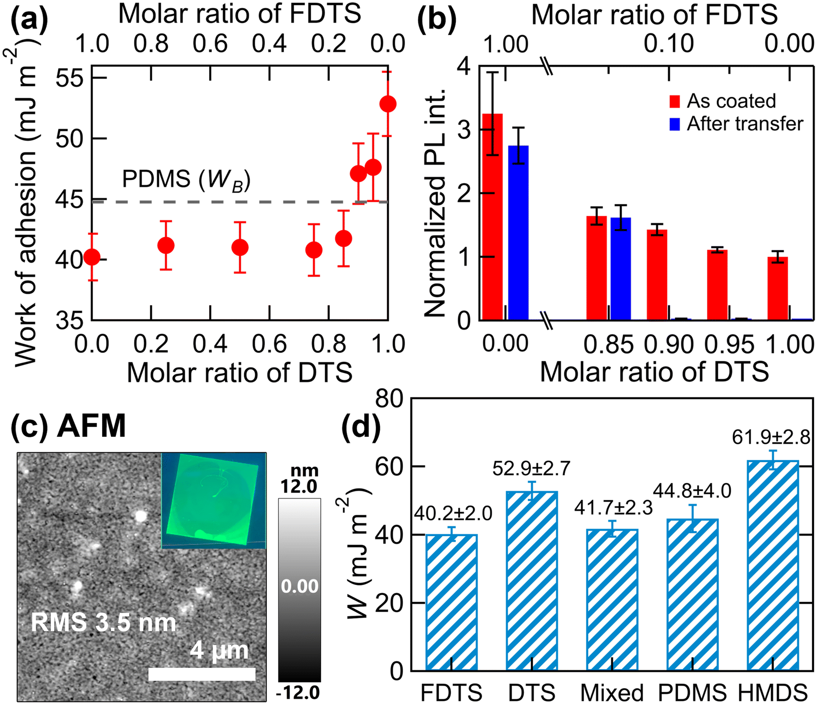 | ||
| Fig. 2 (a) Work of adhesion of the glass substrates treated with mixed silane as a function of the FDTS and DTS mixing ratio (in solution). The broken line represents the work of adhesion of the PDMS stamp (WB). (b) PL intensity of NC films spin-coated on mixed silane-treated substrates (red bars) and PL intensity of NC films on a PDMS stamp after being picked up (blue bars). (c) AFM images of spin-coated NC monolayers on a glass substrate treated with mixed silane (FDTS:DTS = 0.15:0.85). The inset shows a fluorescence microscope image under UV lamp illumination. (d) Comparison of the work of adhesion between the NC monolayer and various material surfaces. | ||
| θ H2O (°) | θ CH2I2 (°) | γ dSV (mJ m−2) | γ hSV (mJ m−2) | W (mJ m−2) | |
|---|---|---|---|---|---|
| Sample | |||||
| NC ML | 90.2 ± 1.3 | 58.6 ± 2.6 | 29.4 ± 2.9 | 2.4 ± 0.5 | |
| HMDS | 84.88 ± 0.3 | 64.9 ± 0.1 | 25.8 ± 0.5 | 5.0 ± 0.2 | 61.9 ± 2.8 |
| PDMS | 109.8 ± 1.4 | 84.7 ± 3.0 | 15.2 ± 2.5 | 0.7 ± 0.3 | 44.8 ± 4.0 |
| PMMA | 69.4 ± 0.5 | 35.5 ± 0.3 | 41.8 ± 1.1 | 7.1 ± 0.3 | 78.3 ± 3.5 |
| FDTS ratio (%) | |||||
| 0 (DTS) | 106.1 ± 0.9 | 71.4 ± 1.5 | 22.1 ± 1.8 | 0.4 ± 0.2 | 52.9 ± 2.7 |
| 5 | 111.0 ± 1.2 | 79.8 ± 2.1 | 17.6 ± 1.9 | 0.3 ± 0.2 | 47.1 ± 2.5 |
| 10 | 110.3 ± 1.1 | 79.2 ± 3.9 | 17.9 ± 2.6 | 0.3 ± 0.2 | 47.6 ± 2.8 |
| 15 | 109.8 ± 1.3 | 90.2 ± 1.1 | 12.6 ± 1.7 | 1.0 ± 0.3 | 41.7 ± 2.3 |
| 25 | 110.1 ± 1.1 | 91.8 ± 0.5 | 11.9 ± 1.4 | 1.2 ± 0.3 | 40.8 ± 2.2 |
| 50 | 109.5 ± 1.0 | 91.6 ± 0.5 | 12.0 ± 1.3 | 1.3 ± 0.2 | 41.0 ± 2.1 |
| 75 | 109.5 ± 0.7 | 91.4 ± 1.1 | 12.1 ± 1.0 | 1.3 ± 0.2 | 41.2 ± 2.0 |
| 100 | 109.6 ± 0.7 | 93.0 ± 0.8 | 11.4 ± 0.9 | 1.4 ± 0.2 | 40.2 ± 2.0 |
The work of adhesion of the pure FDTS- and pure DTS-treated surfaces were below or above that of the PDMS stamp B (WB). Therefore, the work of adhesion of the mixed silane-treated surface was expected to cross this value at a certain mixing ratio. Indeed, as shown in Fig. 2a and Table 1, the work of adhesion reached the same value as WB when the mixing ratio FDTS:DTS = 0.13:0.87, but interestingly, the value of the work of adhesion did not change significantly from pure FDTS until the mixing ratio of DTS exceeded 0.8, and the effect of DTS mixing was not clear in the data.
This nonlinear response is often observed in mixed adsorbed monolayers and could be attributed to differences in the surface reactivities (adsorption coefficients) of FDTS and DTS with the substrate surface, where the surface composition may differ from the mixing ratio in solution.17 Furthermore, even if the surface composition agrees with the mixing ratio in solution, it may have a disproportionate effect on the wettability (surface free energy) and work of adhesion. If we look closely at the data in Table 1, the contact angles with water did not change much when DTS was mixed with FDTS and were close to 110°, whereas the contact angles with CH2I2 changed greatly when the DTS ratio was greater than 0.15 (FDTS of 0.85). This result suggests that the data include both effects (surface composition and disproportionate effects on wettability).
To achieve uniform NC monolayer fabrication on substrate A and successful transfer to PDMS stamp B, we further optimized the FDTS and DTS mixing ratios. Fig. 2b shows the PL intensity of NC films spin-coated on mixed silane-treated substrates (red bars) and the PL intensity of these films on a PDMS stamp after being picked up (blue bars).
All the PL intensity data are normalized to the PL intensity of NC monolayers spin-coated on HMDS-treated substrates, where the formation of monolayers was confirmed in a previous study.13 As shown in the results, the PL intensity of the spin-coated NC film on the FDTS-treated surface was three times stronger than that of the reference monolayer data, indicating multilayer formation on the fluorinated surface. For such multilayer films, transfer onto the PDMS stamp was not achieved due to the decrease in effective contact force caused by the increased surface roughness. A tendency toward multilayer formation was observed but was reduced on the mixed silane-treated surface even when the FDTS mixing ratio was considerably small. On the other hand, the blue bars in Fig. 2b reveal that the transfer of NC films to the PDMS stamp B was only achievable when the FDTS mixing ratio exceeded 0.15 (blue bars shown in Fig. 2b), which is in good agreement with the calculated work of adhesion values. The suitability for spin coating and transfer printing is not determined by the same surface properties; thus, the thresholds of the mixing ratio for each process may differ. Eventually, we determined an FDTS mixing ratio of 0.15 as the optimized condition for both spin-coating homogeneous film formation (nearly monolayer) and transfer to the PDMS stamp (the designed work of adhesion relationships throughout the transfer process is summarized in Fig. 2d). The successful formation of homogeneous NC films was confirmed by fluorescence microscope images under UV lamp illumination (see the inset of Fig. 2c).
Here it should be noted that the use of mixed adsorbents may lead to local surface heterogeneity due to phase separation. To evaluate the morphology of the NC monolayer, we performed atomic force microscope (AFM) observations. Fig. 2c shows an AFM image of the spin-coated NC film on the mixed silane-treated substrates. As reported in a previous paper, a spin-coated film (monolayer) on HMDS-treated substrates is spatially quite uniform, with an RMS roughness value of 2.7 nm.13 For the spin-coated film on the mixed silane-treated substrate, white small protrusions were observed in the AFM image, likely originating from aggregates of FDTS or resulting in NC aggregation. Additionally, the film was slightly more inhomogeneous, with an RMS roughness of 3.5 nm. However, this roughness value is still smaller than the individual NC size (∼9 nm), and it can be regarded as a monolayer film. The PL intensities of the spin-coated film on the mixed silane-treated substrate (red bar in Fig. 2b) and of the film after being picked up onto the PDMS stamp (blue bar in Fig. 2b) were almost unchanged. This feature indicates that efficient transfer from optimized substrate A to PDMS stamp B was achieved despite the increased surface heterogeneity. Presumably, the heterogeneity on the substrate surface did not have a significant effect on the self-assembled NC film, which formed a continuous film due to the strong interactions between the NCs. A detailed analysis of the optical properties of the NC monolayers before and after transfer printing is presented in the next section in comparison with the data from a dual-layer transfer printing technique using a PMMA layer.
2.4. Comparison with dual-layer transfer printing
For comparison with our proposed surface modification method involving FDTS and DTS mixed silanes for transfer printing, we investigated a dual-layer approach, which has been demonstrated in previous studies to control the work of adhesion.7 Here, in this study, a polymethyl methacrylate (PMMA) thin film, which can be easily fabricated by spin-coating (see Methods) on top of an NC monolayer, was used as an adhesive layer.A schematic illustration of dual-layer transfer printing is shown in Fig. 3a. Prior to conducting transfer experiments, we evaluated the feasibility of the dual-layer approach in terms of the work of adhesion. First, the surface free energy of PMMA was determined via contact angle measurements, and the work of adhesion with the NC monolayer (WD′) and the PDMS stamp (WB′) were estimated (see Table 2). The work of adhesion between PMMA and the NC monolayer (WD′) is greater than that between PMMA and PDMS (WB′) and even greater than that between the HMDS-treated surface and the NC monolayer (WC′) (see Table 1), indicating that the dual-layer structure is stably maintained throughout the transfer printing process. Since the work of adhesion of substrate A′ (WA′) should be lower than that between PMMA and PDMS (WB′) for successful transfer, we selected a DTS-treated glass substrate as substrate A′ from the list in Table 1, in consideration of the quality of the monolayer film (see Fig. 2b). In this experimental design, the work of adhesion increases in the order of WA′, WB′, and WC′, suggesting that transfer printing will be successful (see Fig. 3b).
 | ||
| Fig. 3 (a) Schematic illustration of dual-layer transfer printing. A spin-coated LHP NC monolayer on substrate A′ (DTS-treated glass substrate) was picked up by a PDMS stamp B′ after top coating with PMMA and transferred to the same C′ (HMDS-treated glass substrate). (b) Comparison of the work of adhesion between the NC monolayer and various material surfaces for dual-layer printing. | ||
| Sample | θ H2O (°) | θ CH2I2 (°) | γ dSV (mJ m−2) | γ hSV (mJ m−2) | W D′(PMMA/NC ML) (mJ m−2) | W B′(PMMA/PDMS) (mJ m−2) |
|---|---|---|---|---|---|---|
| PMMA | 69.4 ± 0.5 | 35.5 ± 0.3 | 29.4 ± 2.9 | 2.4 ± 0.5 | 78.3 ± 3.5 | 54.7 ± 4.2 |
Fig. 4a presents fluorescence microscope images of NC monolayers fabricated and transferred via the proposed 2 methods. The spin-coated film on the substrate A (mixed FDTS/DTS-treated substrate) and the substrate A′ (DTS-treated substrate) are quite uniform, indicating successful formation of spatially uniform NC monolayers over large areas. The fluorescence microscope images of substrates C and C′ transferred via the direct printing method and dual-layer printing method are less uniform than the images of A and A′. Unidirectional crack structures appeared on substrate C′ due to mechanical stress at the interfaces of the two polymers having different elasticities during the peeling-off process (the peeling direction was from the base of the triangles to the apex). The images of triangles remaining on the PDMS stamp B′ support the above assumption (see the inserted image). The NC monolayer transferred by direct printing with wettability control via FDTS/DTS mixed with silane appeared more spatially uniform, although there were few cracks and breaks caused by the transfer process.
 | ||
| Fig. 4 (a) Fluorescence microscope images of spin-coated NC monolayers on substrates A and A′ and transferred films on substrates C and C′. The inset shows a fluorescence microscope image of the PDMS stamp B′ after it was picked from substrate A′ and transferred to substrate C′, revealing triangle features remaining on the stamp. (b) PL spectra of NC monolayers measured on these substrates (A, A′, C, C′). (c) Histograms of pixel-by-pixel PL intensity distributions obtained from the fluorescence images (pixel size: 2 × 2 μm). | ||
Fig. 4bshows the PL spectra of NC monolayers spin-coated on substrates A and A′ (dashed curves) and after transfer onto substrates C and C′ (solid curves). For both cases, a slight decrease in the PL intensity of approximately 15% but no change in the spectral shape was found compared with those on substrates A and A′. This unchanged spectral shape confirms that the transfer process does not result in typical degradation phenomena such as PL broadening and resonance wavelength shifts due to NC aggregation and changes in size and crystallinity.18,19 In contrast, the slight decrease in the PL intensity implies transfer losses below the resolution of the microscope. The decrease in PL intensity observed during dual-layer printing (A′ and C′) is due to the reduced collection efficiency of emitted light by the objective lens, caused by the top PMMA coating (refractive index: 1.49). Fig. 4c shows the PL intensity distribution in a histogram based on the green PL intensity measured at each pixel (pixel size: 2 × 2 μm) under a fluorescence microscope. Gaussian fitting of the histograms of the emitting region (black curves) excluding the macroscopic defect indicates that the transfer efficiency was approximately 94% for the direct printing method by wettability control and 64% for the dual-layer printing method with PMMA. The width of the intensity distribution does not change, indicating that the spatial uniformity of the NC monolayer is maintained, at least at the microscope resolution. These results demonstrate the high potential of our surface wettability modification approach, both in terms of transfer efficiency and optical properties.
Data on unsuccessful film transfer, which are consistent with predictions based on the work of adhesion calculations, are available in the ESI (Fig. S1†).
2.4. Micropatterning using processed PDMS stamps
Using the established direct printing method with wettability control and the dual-layer printing method with PMMA, micropatterning of NC monolayers using PDMS stamps with arbitrary microstructures was demonstrated.Fig. 5 shows fluorescence microscope images of the micropatterned NC monolayers fabricated via the direct printing method with wettability control via cylindrical patterned PDMS stamps with periodicities of 10, 50, and 100 μm. Clear periodic circular patterns were observed for periods of 100 μm (Fig. 5a) and 50 μm (Fig. 5b), whereas shape distortion was obvious for periods of 10 μm (Fig. 5c), indicating the resolution limit of the current process. The dual-layer approach was unsuccessful because the elastic continuous PMMA film prevented the transfer of the micropattern (data not shown).
 | ||
| Fig. 5 Fluorescence microscope images of micropatterned NC monolayers on target substrates C obtained via the direct printing method with wettability control. PDMS stamps with circular protrusions of (a) 100 μm, (b) 50 μm, and (c) 10 μm periodicity were used. The inset of (c) is an enlarged view. | ||
Patterning NC films at the submicron scale, comparable to the wavelength of light, has the potential to improve device properties through a variety of optical effects.13,20 However, when a third material such as the dual-layer transfer method mentioned above is used, not only the difficulty of transferring patterns but also concerns that the third material may adversely affect the performance of the optoelectronic device via the optical density and electrical conductivity. In this regard, although there is still room for improving the quality of patterned films, our direct transfer method has great potential, especially for industrial applications. In particular, a methodology for stably fabricating uniform NC monolayers through inter-NC self-assembly will be key for future NC device applications.
3. Conclusion
In this study, we proposed a direct printing method employing PDMS stamps via wettability control of substrates using mixed fluorinated silanes and successfully fabricated micropatterned LHP NC self-assembled monolayers. This was achieved by the formation of spatially uniform LHP NC self-assembled monolayers by spin coating and controlling the work of adhesion between the substrates and NCs in the multistep transfer process. The optimal mixing ratio of fluoroalkylsilanes (FDTS) and alkylsilanes (DTS), i.e., FDTS:DTS = 0.15:0.85, was determined from the estimation of the work of adhesion to the NC monolayer through contact angle measurements. This solvent- and heat-free printing method maintained the original PL quality of the NCs throughout the transfer printing process. Compared with the bilayer printing method using PMMA adhesive film, the direct printing method has high potential not only in terms of process convenience but also in terms of film quality, micropattern formation, and especially final optoelectronic device performance by eliminating unnecessary materials in device components. This back-to-basics technique provides crucial information for the field of nanodevices using perovskite NCs, which have excellent optical properties but are of concern for industrial applications due to their chemical fragility.
4. Methods
Synthesis and purification of CsPbBr3 NCs
CsPbBr3 NCs were synthesized via the hot injection method previously reported in our papers.14 A cesium oleate precursor solution was prepared by mixing cesium acetate (240 mg), OA (0.65 mL), and 1-octadecene (ODE) (10 mL) and then degassing and stirring at 80 °C until a clear solution was obtained. The solution was heated to 120 °C to eliminate the formed acetic acid. Subsequently, OA (0.6 mL), OLA (0.5 mL), PbBr2 (69 mg), and ODE (5 mL) were mixed and stirred under vacuum at 100–200 °C until the PbBr2 completely dissolved. The prepared cesium oleate solution (0.4 mL) was then injected into the reaction solution at 170 °C for 5–10 s and then quenched in an ice–water bath. The NCs were purified by centrifugation and redispersed in hexane. To fabricate uniform self-assembled NC monolayers by spin-coating, the purification of NCs (removal of excess ligands and NC aggregates) is crucial, as reported in our previous study.13 The detailed conditions for NC purification are available in our previous study.13NC film fabrication by spin-coating
The NC dispersion in hexane was adjusted to a concentration of 10 mg mL−1 based on absorbance measurements.13,21 For a 1 cm2 substrate, 50 μL of the NC dispersion was spread over the entire substrate surface and left for several seconds to allow NCs to adsorb on the surface. The substrate was then spun at 7000 rpm to remove excess NCs and solvent, except for the adsorbed NC monolayers. Afterward, the sample was dried under vacuum for at least 30 min.Silane treatment of glass substrates
Surface treatments with DTS, FDTS, and mixtures of both silanes were performed in a liquid-phase reaction. For each treatment, the precleaned glass substrates were immersed for 2 hours in hexane containing a total of 5 mM silanes. After immersion, the substrates were rinsed with hexane, dried under N2 gas, and annealed under vacuum at 120 °C for 20 minutes. Finally, the substrates were ultrasonicated at 40 kHz in chloroform (15 minutes at 25 °C) and dried under N2.Surface treatments with HMDS were performed in the gas phase. Precleaned glass substrates were placed in a sealed glass container containing a 1.0 mL droplet of HMDS on the side and exposed to HMDS vapor for 2 h, allowing for vapor-phase treatment.
PDMS stamp preparation
The PDMS stamp was prepared via a previously reported method.22 Sylgard 184 and its curing agent (Sigma-Aldrich, USA) were mixed at a 10:1 weight ratio. After degassing at room temperature under vacuum until all the bubbles were eliminated, the mixture was slowly poured into a glass container with a cleaned Si substrate placed at the bottom and cured by heating under vacuum at 80 °C for 40 min. The mixture was then cured by heating under vacuum at 80 °C for 40 min. Patterned PDMS stamps were fabricated via the same procedure with commercially available mold substrates.
PMMA film preparation
PMMA was dissolved in toluene at 0.5 vol%, and 200 μL of the solution was applied onto the substrate and spin-coated at 4000 rpm for 1 min. According to the AFM measurements, the thickness of the PMMA layer was approximately 100 nm.Contact angle measurement and estimation of the surface free energy
The contact angles of two different liquids on each material surface were measured using by a commercial contact angle meter (CA-X, Kyowa Interface Science, Japan). The surface free energy was estimated from the contact angle values using the following equations:23

Here, γLV1 and γLV2 are the surface free energies of liquids 1 and 2, respectively, and θ1 and θ2 are the contact angles. Throughout this study, pure water (γLV1 = 72.8 mN m−1,  = 21.8 mN m−1,
  = 51.0 mN m−1) and Ch2I2 (γLV2 = 50.8 mN m−1,
  = 50.8 mN m−1,
  = 0 mN m−1) were used as probe liquids.24,25
Fluorescence microscope observation and PL measurement
Fluorescence microscope images and PL spectra of the NC films were collected by using an epifluorescence microscope (ECLIPSE 80i, Nikon, Japan) with a mercury lamp, an excitation filter (400–440 nm), and a PMA-12 photonic multichannel analyzer (Hamamatsu, Japan).Data availability
The data supporting this article have been included as part of the ESI.†Conflicts of interest
There are no conflicts to declare.Acknowledgements
This work was supported by JSPS KAKENHI grant number 19H05627 and 24H00802.References
- Q. A. Akkerman, G. Rainò, M. V. Kovalenko and L. Manna, Nat. Mater., 2018, 17, 394–405 CrossRef CAS PubMed.
- J. Shamsi, A. S. Urban, M. Imran, L. De Trizio and L. Manna, Chem. Rev., 2019, 119, 3296–3348 CrossRef CAS PubMed.
- L. Protesescu, S. Yakunin, M. I. Bodnarchuk, F. Krieg, R. Caputo, C. H. Hendon, R. X. Yang, A. Walsh and M. V. Kovalenko, Nano Lett., 2015, 15, 3692–3696 CrossRef CAS PubMed.
- S. N. Raja, Y. Bekenstein, M. A. Koc, S. Fischer, D. Zhang, L. Lin, R. O. Ritchie, P. Yang and A. P. Alivisatos, ACS Appl. Mater. Interfaces, 2016, 8, 35523–35533 CrossRef CAS PubMed.
- T. Leijtens, G. E. Eperon, N. K. Noel, S. N. Habisreutinger, A. Petrozza and H. J. Snaith, Adv. Energy Mater., 2015, 5, 1500963 CrossRef.
- S. Jia, G. Li, P. Liu, R. Cai, H. Tang, B. Xu, Z. Wang, Z. Wu, K. Wang and X. W. Sun, Adv. Funct. Mater., 2020, 30, 1910817 CrossRef CAS.
- J. I. Kwon, G. Park, G. H. Lee, J. H. Jang, N. J. Sung, S. Y. Kim, J. Yoo, K. Lee, H. Ma, M. Karl, T. J. Shin, M. H. Song, J. Yang and M. K. Choi, Sci. Adv., 2022, 8, eadd0697 CrossRef CAS PubMed.
- D. Liu, K. Weng, S. Lu, F. Li, H. Abudukeremu, L. Zhang, Y. Yang, J. Hou, H. Qiu, Z. Fu, X. Luo, L. Duan, Y. Zhang, H. Zhang and J. Li, Sci. Adv., 2022, 8, eabm8433 CrossRef CAS PubMed.
- G. H. Lee, K. Kim, Y. Kim, J. Yang and M. K. Choi, Nano-Micro Lett., 2023, 16, 45 CrossRef PubMed.
- J. Yoo, K. Lee, U. J. Yang, H. H. Song, J. H. Jang, G. H. Lee, M. S. Bootharaju, J. H. Kim, K. Kim, S. I. Park, J. D. Seo, S. Li, W. S. Yu, J. I. Kwon, M. H. Song, T. Hyeon, J. Yang and M. K. Choi, Nat. Photonics, 2024, 18, 1105–1112 CrossRef CAS.
- S. De Wolf, J. Holovsky, S. J. Moon, P. Löper, B. Niesen, M. Ledinsky, F. J. Haug, J. H. Yum and C. Ballif, J. Phys. Chem. Lett., 2014, 5, 1035–1039 CrossRef CAS PubMed.
- D. Xing, C.-C. Lin, Y.-L. Ho, Y.-C. Lee, M.-H. Chen, B.-W. Lin, C.-W. Chen and J.-J. Delaunay, Small, 2022, 18, 2204070 CrossRef CAS PubMed.
- Y. Kajino, Y. Aida, Y. Arima, Y. J. Lee and K. Tamada, ACS Appl. Nano Mater., 2024, 7, 9095–9105 CrossRef CAS.
- J. Leng, T. Wang, Z. K. Tan, Y. J. Lee, C. C. Chang and K. Tamada, ACS Omega, 2022, 7, 565–577 CrossRef CAS PubMed.
- D. K. Owens and R. C. Wendt, J. Appl. Polym. Sci., 1969, 13, 1741–1747 CrossRef CAS.
- T. Meng, Y. Zheng, D. Zhao, H. Hu, Y. Zhu, Z. Xu, S. Ju, J. Jing, X. Chen, H. Gao, K. Yang, T. Guo, F. Li, J. Fan and L. Qian, Nat. Photonics, 2022, 16, 297–303 CrossRef CAS.
- K. Tamada, M. Hara, H. Sasabe and W. Knoll, Langmuir, 1997, 13, 1558–1566 CrossRef CAS.
- Y. Tong, E.-P. Yao, A. Manzi, E. Bladt, K. Wang, M. Döblinger, S. Bals, P. Müller-Buschbaum, A. S. Urban, L. Polavarapu and J. Feldmann, Adv. Mater., 2018, 30, 1801117 CrossRef PubMed.
- F. Chen, M. Imran, L. Pasquale, M. Salerno and M. Prato, Mater. Res. Bull., 2021, 134, 111107 CrossRef CAS.
- S. V. Makarov, V. Milichko, E. V. Ushakova, M. Omelyanovich, A. Cerdan Pasaran, R. Haroldson, B. Balachandran, H. Wang, W. Hu, Y. S. Kivshar and A. A. Zakhidov, ACS Photonics, 2017, 4, 728–735 CrossRef CAS.
- J. Maes, L. Balcaen, E. Drijvers, Q. Zhao, J. De Roo, A. Vantomme, F. Vanhaecke, P. Geiregat and Z. Hens, J. Phys. Chem. Lett., 2018, 9, 3093–3097 CrossRef CAS PubMed.
- S. Y. Kim, J. I. Kwon, H. H. Song, G. H. Lee, W. S. Yu, S. Li, M. K. Choi and J. Yang, Appl. Surf. Sci., 2023, 610, 155579 CrossRef CAS.
- M. Annamalai, K. Gopinadhan, S. A. Han, S. Saha, H. J. Park, E. B. Cho, B. Kumar, A. Patra, S.-W. Kim and T. Venkatesan, Nanoscale, 2016, 8, 5764–5770 RSC.
- F. M. Fowkes, J. Phys. Chem., 1963, 67, 2538–2541 CrossRef CAS.
- B. Janczuk, E. Chibowski, J. M. Bruque, M. L. Kerkeb and F. G. Caballero, J. Colloid Interface Sci., 1993, 159, 421–428 CrossRef CAS.
Footnote |
| † Electronic supplementary information (ESI) available. See DOI: https://doi.org/10.1039/d4nr05088f |
| This journal is © The Royal Society of Chemistry 2025 |