
 Open Access Article
 This Open Access Article is licensed under a
 Creative Commons Attribution 3.0 Unported Licence
Growing and nanomanipulating heterostructures of α-bismuthene in a nearly isolated state†
Antonio J.
Martínez-Galera
 *abc and
José M.
Gómez-Rodríguez‡
bcd
*abc and
José M.
Gómez-Rodríguez‡
bcd
aDepartamento de Física de Materiales, Universidad Autónoma de Madrid, Madrid E-28049, Spain. E-mail: antonio.galera@uam.es
bCondensed Matter Physics Center (IFIMAC), Universidad Autónoma de Madrid, Madrid E-28049, Spain
cInstituto Nicolás Cabrera, Universidad Autónoma de Madrid, Madrid E-28049, Spain
dDepartamento de Física de la Materia Condensada, Universidad Autónoma de Madrid, Madrid E-28049, Spain
First published on 17th February 2025
Abstract
The growth of vertical heterostructures, which incorporate bismuthene with minimal coupling to adjacent materials, is pursued to fully exploit the exceptional properties intrinsic to the 2D allotropic forms of bismuth. Here, the growth of vertical heterostructures of ultrathin α-bismuthene and one-atom-thick layers of hexagonal boron nitride (h-BN) supported on Rh(110) surfaces is reported. Scanning tunneling microscopy (STM) characterization shows that the sample morphology is dominated by the presence of ultrathin α-bismuthene islands, with a lower thickness limit of a paired bilayer, randomly scattered over the h-BN surface. Unlike previous studies on heterostructures combining α-bismuthene with different 2D materials, which only allowed specific relative angles between the atomic lattices of both constituents, the Bi structures grown here can adopt any in-plane orientation relative to the underlying h-BN/Rh(110) surface, although certain twist angles are preferred. The greater rotational variety found in this study suggests a weaker interaction between bismuthene and h-BN, meaning that these islands could be the most weakly coupled 2D Bi nanocrystals to a substrate reported to date. Additionally, in pursuit of precise control over the spatial distribution of the islands on the h-BN/Rh(110) surface, they have been nanomanipulated using the STM tip.
Introduction
van der Waals heterostructures provide a platform for observing novel physical phenomena and currently hold significant potential for implementation as building blocks in future technology.1–8 The van der Waals epitaxy inherent to the formation of such systems allows the 2D materials in the heterostructure to retain most of their intrinsic properties while minimizing the stress associated with the lattice mismatch that dominates conventional heteroepitaxy.9 Atomically thin Bi layers, which exhibit properties such as quantum size effects, Dirac cones, topological edge states, and large spin–orbit coupling, constitute a fascinating subject of study within the 2D materials family.10–13The most stable configurations of ultrathin Bi films are the hexagonal Bi(111) and the pseudocubic Bi(110) structures. The former, also known as β-bismuthene,14 is characterized by a honeycomb arrangement. Conversely, the Bi(110) structure, also known as α-bismuthene,14 according to previous research can either form a stack of bulk truncated Bi(110) planes or a black phosphorus (BP)-like arrangement, in which the formation of interlayer covalent bonds creates paired bilayers saturating all the dangling bonds of the two (110) planes.15 While in the first case, islands with both even and odd numbers of layers can be found, the latter only admits islands with an even number of atomic planes.16
Previous studies of van der Waals heterostructures comprising ultrathin Bi films are scarce and have mainly focused on combinations with graphene17–19 or different 2D transition metal dichalcogenides, for instance, HfTe2,20 TiSe2,21 and NbSe2.22 In these cases, Bi adopted the α-bismuthene structure, which was found to be oriented along specific directions of the 2D material placed below. This suggests that, although weak, the interaction between α-bismuthene and these 2D materials is sufficient to force the former to be oriented along specific angles with respect to the atomic lattice of the other constituent of the heterostructure. This raises the question of whether it is possible to achieve heterostructures with an even weaker interaction between bismuthene and the other 2D material.
Despite the advantages of using an insulating support to achieve weak interactions with 2D materials on top, thus better exploiting their intrinsic properties,8,23 ultrathin bismuthene films have mostly been reported on conducting and semiconducting surfaces. On the other hand, it should also be taken into account that the properties of ultrathin Bi films are highly dependent on their thickness.12,24 Additionally, in the pursuit of a collective response from heterostructures, other key factors potentially influencing the overall performance are the density of Bi islands and the possible coexistence of ones oriented differently over the supporting surface. Nevertheless, in all the cases mentioned above, the as-grown films were randomly scattered over the surface, exhibiting different in-plane orientations and a variety of heights for a given amount of Bi. Therefore, top-down approaches are demanded to eliminate the coexistence of islands with different heights and in-plane orientations while precisely controlling island density to fully exploit the potential of Bi-based heterostructures. Here, the first heterostructures comprising ultrathin bismuthene films and one-atom-thick layers of the insulating material hexagonal boron nitride (h-BN) are reported. Specifically, Bi islands exhibiting an α-bismuthene atomic arrangement have been grown under ultrahigh vacuum (UHV) conditions on h-BN/Rh(110) surfaces. This supporting surface was chosen to pursue the goal of achieving α-bismuthene layers with minimal interactions with their local environment. Thus, to ensure that the intrinsic properties of h-BN, which make this 2D material an excellent decoupling layer, are preserved to the greatest extent, it must be grown on metal surfaces, giving rise to a weak interfacial coupling. In this sense, previous research has demonstrated that the symmetry mismatch between the atomic arrangements of the Rh(110) surface and 2D materials such as graphene and h-BN allows these materials to retain most of their intrinsic properties when grown on top.25–28 The study of the rotational variety of α-bismuthene on h-BN/Rh(110) performed in this work suggests the weakest coupling observed to date between bismuthene and any other 2D material. This success in the growth of nearly isolated α-bismuthene could be crucial for future applications, considering the intrinsic properties of this 2D material. For instance, ideal 2D α-bismuthene exhibits robust quantum spin Hall states and a band gap linked to the bulk bands. Due to these properties, this 2D material is promising for applications in spintronics, such as long-distance spin transport and spin-to-charge conversion, as well as in topotronic devices operating efficiently at room temperature.29 Furthermore, the as-grown islands have been accurately manipulated using a top-down approach, offering ultimate control over their spatial distribution via scanning tunneling microscopy (STM).
Experimental
The experiments were performed in a UHV system, hosting a home-built STM for the atomic-scale analysis of samples.30,31 This experimental system is also equipped with Low Energy Electron Diffraction (LEED) optics as a complementary tool for sample characterization.Rh(110) single crystal surfaces were prepared by Ar+ bombardment with an energy of the incident ions of 1 keV, followed by annealing to 1200 K at an oxygen partial pressure of 2 × 10⁻⁶ Torr. Afterwards, the sample was further heated at 1200 K for 300 s and flash annealed to 1370 K. Over the as-obtained Rh(110) surfaces, h-BN monolayers were grown by chemical vapor deposition (CVD), using borazine (B3N3H6) as the precursor. Specifically, the surface of the Rh(110) supports held at 800 ºC was exposed to a borazine partial pressure of 3.5 × 10⁻⁸ Torr for 35 minutes. Then, bismuthene growth was carried out by Bi sublimation from a Knudsen cell type evaporator onto the h-BN/Rh(110) samples at room temperature.
STM data were acquired and represented by using the WSxM software.32 STM imaging was performed at the constant current mode with the bias voltage applied to the sample while the tip was grounded.
Results and discussion
Fig. 1 shows representative STM images illustrating how sample morphology varies with the amount of Bi deposited over the h-BN/Rh(110) surfaces. As observed, at low coverages, Bi arranges into islands with almost regular shapes, which are found scattered over the h-BN/Rh(110) surfaces. At larger Bi coverages, the resulting islands tend to exhibit markedly elongated shapes. Finally, larger deposited amounts of Bi give rise to a network of islands, which become interconnected. Besides the geometry and spatial distribution of islands, their heights also vary with the amount of Bi deposited, with larger heights observed as the quantity of Bi increases. | ||
| Fig. 1 Spatial distribution of the bismuthene islands. (a)–(c) STM images illustrating the evolution of sample morphology with increasing Bi coverage deposited over the h-BN/Rh(110) surfaces. The greenish hue observed in the STM images is associated with the h-BN surface, while the pinkish tones correspond to islands of α-bismuthene, which have larger heights as the lighter the observed tone is. Tunneling parameters: (a) Vs = +1.0 V; IT = 0.1 nA, size: 290 × 290 nm2; (b) Vs = +1.0 V; IT = 0.1 nA, size: 290 × 290 nm2; (c) Vs = +1.0 V; IT = 0.1 nA, size: 290 × 290 nm2. | ||
The variation of sample morphology with the Bi coverage is consistent with a Volmer-Weber growth mode, which is generally associated with a larger interaction between adatoms than between them and the substrate. In turn, the nearly regular shapes of the islands suggest that Bi atoms are packed into a well-ordered structure due to cohesive interactions. This atomic packing will be further discussed along with the analysis of the data summarized in Fig. 2. Additionally, the in-plane orientation of the Bi arrangement with respect to the h-BN/Rh(110) surface underneath will be analyzed in Fig. 3.
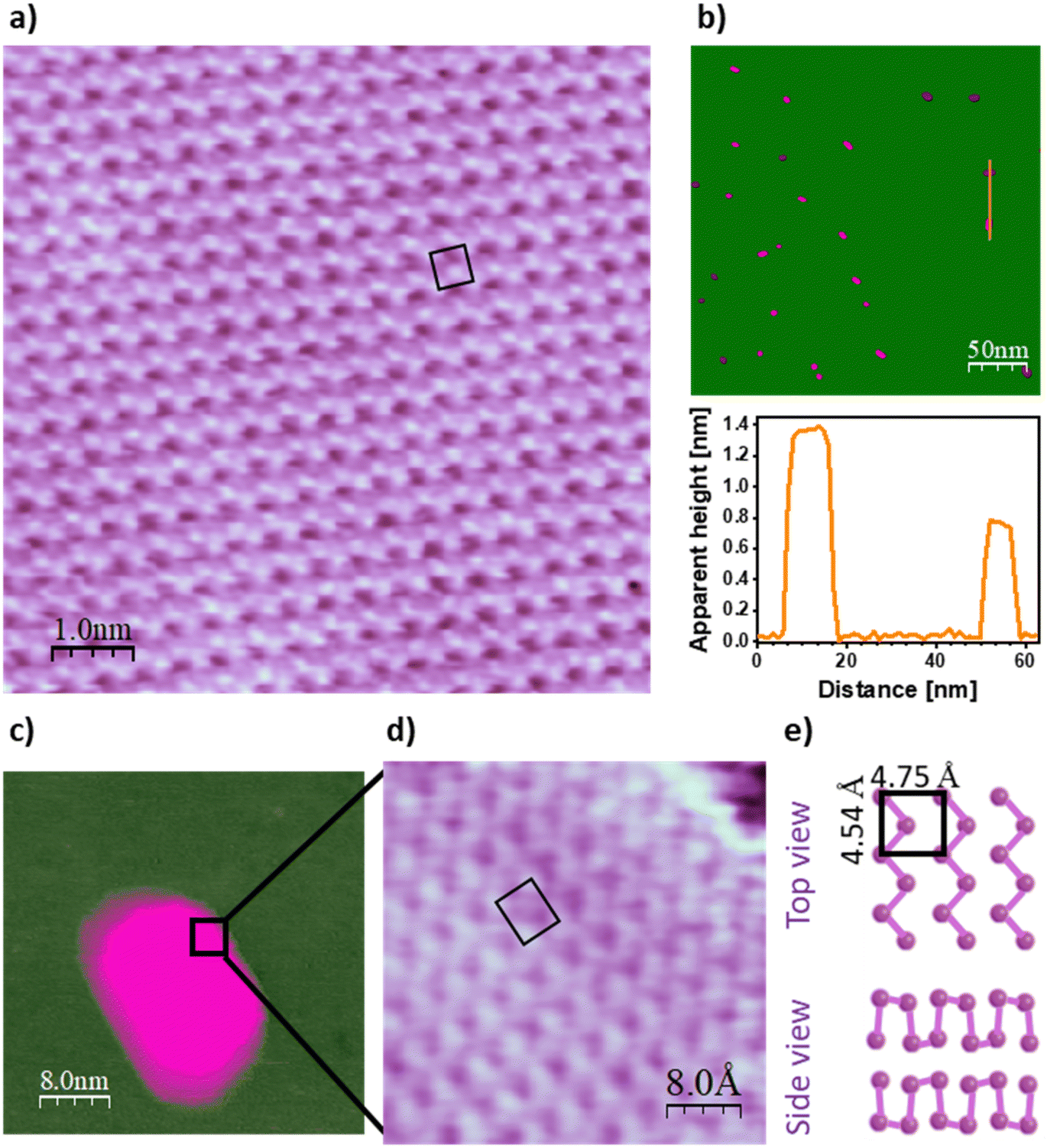 | ||
| Fig. 2 Internal structure of bismuthene islands. (a) Atomically resolved STM image displaying the arrangement of Bi atoms on the surface of an island; (b) STM image displaying bismuthene islands scattered over an h-BN/Rh(110) surface (top panel) and topography profile along the orange line (bottom panel); (c) STM image acquired over a region encompassing a bismuthene island; (d) atomically resolved STM image acquired within the region indicated by the square overlaid in (c), where it is observed the atomic arrangement around the island edge. (e) Schematic representation of the α-bismuthene planes stacked forming two paired bilayers. The greenish hue observed in the STM images is associated with the h-BN surface, while the pinkish tones correspond to islands of α-bismuthene, which have larger heights, the lighter the observed tone is. Tunneling parameters: (a) Vs = +1.21 V; IT = 0.31 nA, size: 8 × 8 nm2; (b) Vs = +1.0 V; IT = 0.1 nA, size: 290 × 290 nm2; (c) Vs = +1.0 V; IT = 0.1 nA, size: 40 × 40 nm2; (d) Vs = 0.12 V; IT = 4.53 nA, size: 4 × 4 nm2. | ||
 | ||
| Fig. 3 Relative orientation between the α-bismuthene lattice and the h-BN/Rh(110) support underneath. (a) LEED pattern representative of the as-grown h-BN/Rh(110) surfaces; (b) LEED pattern acquired after α-bismuthene growth on h-BN/Rh(110); (c) schematics illustrating the origin of the different diffraction features observed in the LEED pattern shown in panel (b). Electron energy (a) and (b) 40 eV. | ||
Fig. 2 summarizes the experimental findings about the internal structure of the islands. Specifically, Fig. 2a shows an atomically resolved STM image acquired on the surface of a Bi island. A motif with rectangular geometry and lateral dimensions of 4.5 × 4.8 Å2 is observed. This rectangular structure is also displayed in the STM topograph of Fig. 2d, which was acquired around the edge of the island imaged in Fig. 2c. Concerning the vertical dimensions of the atomic packing, the apparent heights of the islands are roughly integer multiples of ∼0.65 nm, as shown in Fig. 2b.
The existence of an ordered layout with well-defined lateral and vertical dimensions is a clear indication that the atomic arrangement proceeds according to a specific crystal structure. To interpret the information provided in Fig. 2 about the atomic packing within the islands, it is convenient to keep in mind the crystal structure of bulk Bi. Specifically, Bi crystal can be understood as a rhombohedral arrangement with two atoms per unit cell.33 The (110) plane of this structure is characterized by a rectangular lattice with lateral dimensions of 4.54 × 4.75 Å2, comprising two atoms with slightly different heights along the normal to the plane.33 Both the atomic ordering and the lateral dimensions of the Bi motif grown here are consistent with that picture, suggesting that Bi arranges over the h-BN/Rh(110) surface following a similar packing to that of the (110) planes of bulk Bi. Interestingly, throughout the structural analysis conducted in this work, a domain boundary was never observed within any of the islands studied. This may indicate that the islands are single crystals.
Concerning the vertical dimensions, as mentioned above, the apparent heights of the islands are found to invariably be integer multiples of ∼0.65 nm, which roughly coincides with two times the separation distance between consecutive (110) planes in bulk Bi. This fact, together with the experimental findings discussed in the preceding paragraph, constitutes a clear indication that the islands are composed of stacks of the α-bismuthene paired bilayers, consistent with an atomic arrangement according to a BP-like structure. Accordingly, similar arrangements of Bi have been previously observed on other 2D materials such as graphene,17–19 HfTe2,20 TiSe2,21 and NbSe2.22 In these cases, the preference for the coupling into bilayers was ascribed to the establishment of interlayer bonds between undercoordinated Bi atoms, avoiding the presence of dangling bonds (see Fig. 2e).
Once the internal structure of the islands has been addressed, Fig. 3 tackles the analysis of possible preferred relative orientations between the atomic packing of Bi and the underlying h-BN/Rh(110) surfaces. Specifically, Fig. 3b shows a LEED pattern acquired on a sample with α-bismuthene islands grown over an h-BN/Rh(110) surface. As a reference to better interpret it, a LEED pattern representative of single layer h-BN grown on Rh(110) is provided in Fig. 3a, where two sets of spots with hexagonal symmetry associated, respectively, to the atomic lattices of the equivalent rotational domains R-26.3 and R-33.7 are observed (see blue and red dashed arrows).25–27 The comparison of both patterns shows that the diffraction features arising after the growth of the α-bismuthene islands consist of a circumference and two sets of well-defined spots (see blue and red solid arrows), whose origin is discussed in the next paragraph.
A schematic providing a possible interpretation of the different diffraction features observed in the LEED patterns obtained after the growth of the α-bismuthene islands is shown in Fig. 3c. According to this picture, the green circumference represents the wide rotational variety of α-bismuthene on the h-BN/Rh(110) surface. Amongst this variety, the set of spots represented by blue circumferences is associated with the orientation of the α-bismuthene unit cell with the longer side aligned, or nearly, with a zig-zag direction of the R-26.3 rotational domain of h-BN over the Rh(110) support. Accordingly, the shorter side of the unit cell must be parallel, or nearly, to the armchair direction of h-BN. Likewise, their counterpart spots represented by the red circumferences are associated with the same Bi arrangement over the R-33.7 rotational domain of the h-BN/Rh(110) surface. The existence of the circumference highlighted in green shows that any orientation between the atomic lattices of α-bismuthene and the underlying h-BN surface is found to coexist in the samples. This finding contrasts with the previously available literature reporting that α-bismuthene exhibits only specific orientations with respect to other 2D materials placed underneath. For example, in the case of monolayer graphene grown on SiC, the zig-zag directions of the Bi(110) planes grown on top were found to be nearly aligned with the armchair directions of graphene.17 Likewise, the rectangular unit cell of Bi(110) was reported to be rotated by 45° relative to the hexagonal arrangement of HfTe2.20 When grown on TiSe2, the rectangular layout of Bi(110) was observed to align with the packing direction of the outermost Se atoms.21 In the case of NbSe2, a combination of STM and density functional theory (DFT) suggested an atomic arrangement in which the shorter axis of Bi(110) aligns with the zig-zag direction of NbSe2.22 The unprecedented rotational freedom of α-bismuthene found in the present work suggests that its interaction with h-BN is among the weakest reported for this polymorph of Bi in relation to its supporting surface, if not the weakest.
As outlined in the introduction, exploiting the full potential of the exceptional properties of α-bismuthene could require controlling the density and the type of islands over the support, pursuing a collective effect. In this respect, Fig. 4 displays a series of STM images acquired on the same region of a sample along sequential removal of the islands. For this purpose, after the acquisition of each image, the scan was stopped, and the tip was placed over the Bi island to be removed. Afterwards, the feedback loop was opened, and the tip approached towards the selected island. After retracting the tip, connecting the feedback loop again, and enabling the scan over the same sample region, the selected island was no longer over the surface. As examples, Fig. 4b and c show two STM images consecutively acquired after the removal of the islands highlighted in Fig. 4a and 4b, respectively. Each yellow circumference indicates the island that was removed after the acquisition of the image, while the end of the arrow in the consecutive topograph points towards the empty room left behind after the removal. As observed, islands are removed regardless of their height, position or orientation (see the ESI† for the whole sequence). Therefore, this procedure can be used to accurately control the density and the type of islands resting over the h-BN/Rh(110) surface. In line with this, as inferred from apparent height profiles like the one displayed in Fig. 2b, a uniform thickness in the as-grown films is not directly achievable as islands with varying heights are found to coexist over the h-BN/Rh(110) surface. Consequently, the island removal procedure could be used, for instance, as a top-down approach to achieve thickness uniformity in a given region of the h-BN surface by only keeping islands matching the desired height.
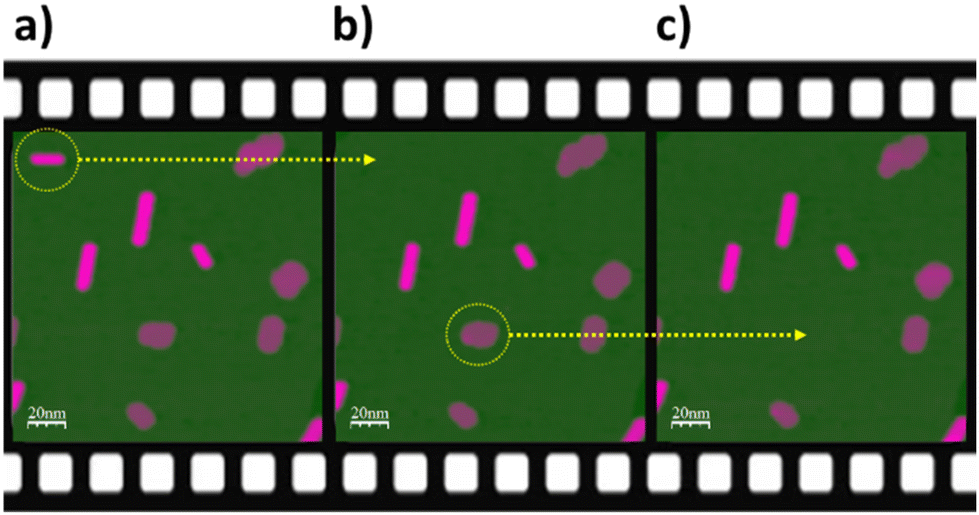 | ||
| Fig. 4 Nanomanipulation of α-bismuthene islands. (a)–(c) Sequence of STM images acquired after the consecutive removal of two islands. In each image, the yellow circumference highlights the island removed after the scanning was stopped, while the arrow in the next topograph indicates the empty room left behind after the removal. The greenish hue observed in the STM images is associated with the h-BN surface, while the pinkish tones correspond to islands of α-bismuthene, which have larger heights, the lighter the observed tone is. Tunneling parameters: Vs = +0.39 V; IT = 0.1 nA, size: 160 × 160 nm2 for the three images. | ||
Conclusions
In summary, α-bismuthene islands are grown under UHV conditions on one-atom-thick h-BN resting over Rh(110) supports. Islands exhibit varying thicknesses as a function of the deposited amount of Bi with the lower limit of a paired bilayer. Atomically resolved STM images acquired over the islands show a rectangular layout with two atoms per unit cell, which is characteristic of Bi(110) planes. LEED patterns demonstrate the existence of preferred in-plane relative orientations between both constituents of the heterostructure, although they also show that every twist angle between the atomic structures of α-bismuthene and h-BN is found over the supporting Rh(110) surface. This rotational variety is unprecedented for heterostructures of α-bismuthene grown on other 2D materials. It suggests that these bismuthene islands are the weakest ones coupled to the 2D material placed underneath reported to date. Through a top-down approach based on nanomanipulation with the STM tip, the spatial distribution of the islands is accurately modified, enabling the selection of the density, size and relative orientations of the α-bismuthene-h-BN heterostructures that remain over the metal support.Data availability
Data are available upon request.Conflicts of interest
There are no conflicts to declare.Acknowledgements
The authors dedicate this work to the memory of Prof. José María Gómez-Rodríguez, a personal friend, mentor and colleague. Financial support from the Spanish MICINN through Projects No. PID2020-116619GA-C22 and No. TED2021-131788A-I00 and from the Comunidad de Madrid and the Universidad Autónoma de Madrid through project SI3/PJI/2021-00500 is gratefully acknowledged.References
- A. K. Geim and I. V. Grigorieva, Nature, 2013, 499, 419–425 CrossRef CAS PubMed.
- T. Georgiou, R. Jalil, B. D. Belle, L. Britnell, R. V. Gorbachev, S. V. Morozov, Y.-J. Kim, A. Gholinia, S. J. Haigh, O. Makarovsky, L. Eaves, L. A. Ponomarenko, A. K. Geim, K. S. Novoselov and A. Mishchenko, Nat. Nanotechnol., 2013, 8, 100–103 CrossRef CAS PubMed.
- X. Hong, J. Kim, S.-F. Shi, Y. Zhang, C. Jin, Y. Sun, S. Tongay, J. Wu, Y. Zhang and F. Wang, Nat. Nanotechnol., 2014, 9, 682–686 CrossRef CAS PubMed.
- X. Qian, J. Liu, L. Fu and J. Li, Science, 2014, 346, 1344–1347 CrossRef CAS PubMed.
- D. Deng, K. S. Novoselov, Q. Fu, N. Zheng, Z. Tian and X. Bao, Nat. Nanotechnol., 2016, 11, 218–230 CrossRef CAS PubMed.
- Y. Liu, N. O. Weiss, X. Duan, H.-C. Cheng, Y. Huang and X. Duan, Nat. Rev. Mater., 2016, 1, 16042 CrossRef CAS.
- K. S. Novoselov, A. Mishchenko, A. Carvalho and A. H. Castro Neto, Science, 2016, 353, aac9439 CrossRef CAS PubMed.
- Y. Cao, V. Fatemi, A. Demir, S. Fang, S. L. Tomarken, J. Y. Luo, J. D. Sanchez-Yamagishi, K. Watanabe, T. Taniguchi, E. Kaxiras, R. C. Ashoori and P. Jarillo-Herrero, Nature, 2018, 556, 80–84 CrossRef CAS PubMed.
- L. A. Walsh and C. L. Hinkle, Appl. Mater. Today, 2017, 9, 504–515 CrossRef.
- H. Asahi, T. Humoto and A. Kawazu, Phys. Rev. B, 1974, 9, 3347–3356 CrossRef CAS.
- Y. M. Koroteev, G. Bihlmayer, J. E. Gayone, E. V. Chulkov, S. Blügel, P. M. Echenique and P. Hofmann, Phys. Rev. Lett., 2004, 93, 046403 CrossRef PubMed.
- G. Bian, X. Wang, T. Miller, T. C. Chiang, P. J. Kowalczyk, O. Mahapatra and S. A. Brown, Phys. Rev. B: Condens. Matter Mater. Phys., 2014, 90, 195409 CrossRef.
- Y. Lu, W. Xu, M. Zeng, G. Yao, L. Shen, M. Yang, Z. Luo, F. Pan, K. Wu, T. Das, P. He, J. Jiang, J. Martin, Y. P. Feng, H. Lin and X.-S. Wang, Nano Lett., 2015, 15, 80–87 CrossRef CAS PubMed.
- S. Zhang, M. Xie, F. Li, Z. Yan, Y. Li, E. Kan, W. Liu, Z. Chen and H. Zeng, Angew. Chem., Int. Ed., 2016, 55, 1666–1669 CrossRef CAS PubMed.
- K. Nagase, I. Kokubo, S. Yamazaki, K. Nakatsuji and H. Hirayama, Phys. Rev. B, 2018, 97, 195418 CrossRef CAS.
- Y. M. Koroteev, G. Bihlmayer, E. V. Chulkov and S. Blüegel, Phys. Rev. B: Condens. Matter Mater. Phys., 2008, 77, 045428 CrossRef.
- T. Hu, X. Hui, X. Zhang, X. Liu, D. Ma, R. Wei, K. Xu and F. Ma, J. Phys. Chem. Lett., 2018, 9, 5679–5684 CrossRef CAS PubMed.
- J. Koch, S. Sologub, C. Ghosal, T. Tschirner, A. Chatterjee, K. Pierz, H. W. Schumacher and C. Tegenkamp, Phys. Rev. B, 2024, 109, 235107 CrossRef CAS.
- J. Koch, C. Ghosal, S. Sologub and C. Tegenkamp, J. Phys.: Condens. Matter, 2024, 36, 065701 CrossRef CAS PubMed.
- E. Xenogiannopoulou, D. Tsoutsou, P. Tsipas, S. Fragkos, S. Chaitoglou, N. Kelaidis and A. Dimoulas, Nanotechnology, 2022, 33, 015701 CrossRef CAS PubMed.
- X. Dong, Y. Li, J. Li, X. Peng, L. Qiao, D. Chen, H. Yang, X. Xiong, Q. Wang, X. Li, J. Duan, J. Han and W. Xiao, J. Phys. Chem. C, 2019, 123, 13637–13641 CrossRef CAS.
- L. Peng, J. Qiao, J.-J. Xian, Y. Pan, W. Ji, W. Zhang and Y.-S. Fu, ACS Nano, 2019, 13, 1885–1892 CAS.
- C. R. Dean, A. F. Young, I. Meric, C. Lee, L. Wang, S. Sorgenfrei, K. Watanabe, T. Taniguchi, P. Kim, K. L. Shepard and J. Hone, Nat. Nanotechnol., 2010, 5, 722–726 CrossRef CAS PubMed.
- A. K. Kundu, G. Gu and T. Valla, ACS Appl. Mater. Interfaces, 2021, 13, 33627–33634 CrossRef CAS PubMed.
- A. J. Martínez-Galera and J. M. Gómez-Rodríguez, Nano Res., 2018, 11, 4643–4653 CrossRef.
- A. J. Martínez-Galera and J. M. Gómez-Rodríguez, Nano Res., 2019, 12, 1217–1218 CrossRef.
- A. J. Martínez-Galera and J. M. Gómez-Rodríguez, J. Phys. Chem. C, 2019, 123, 1866–1873 CrossRef.
- A. J. Martínez-Galera, H. Guo, M. D. Jiménez-Sánchez, E. G. Michel and J. M. Gómez-Rodríguez, Carbon, 2023, 205, 294–301 CrossRef.
- X. Liu, S. Zhang, S. Guo, B. Cai, S. A. Yang, F. Shan, M. Pumera and H. Zeng, Chem. Soc. Rev., 2020, 49, 263–285 RSC.
- O. Custance, S. Brochard, I. Brihuega, E. Artacho, J. M. Soler, A. M. Baró and J. M. Gómez-Rodríguez, Phys. Rev. B: Condens. Matter Mater. Phys., 2003, 67, 235410 CrossRef.
- A. J. Martinez-Galera and J. M. Gomez-Rodriguez, J. Phys. Chem. C, 2011, 115, 11089–11094 CrossRef CAS.
- I. Horcas, R. Fernandez, J. M. Gomez-Rodriguez, J. Colchero, J. Gomez-Herrero and A. M. Baro, Rev. Sci. Instrum., 2007, 78, 013705 CrossRef CAS PubMed.
- P. Hofmann, Prog. Surf. Sci., 2006, 81, 191–245 CrossRef CAS.
Footnotes |
| † Electronic supplementary information (ESI) available: A file with a movie is included as ESI to illustrate the high precision of the nanomanipulation procedure. See DOI: https://doi.org/10.1039/d4nr04927f |
| ‡ Deceased. |
| This journal is © The Royal Society of Chemistry 2025 |