
 Open Access Article
 This Open Access Article is licensed under a
 Creative Commons Attribution 3.0 Unported Licence
Understanding fatigue and recovery mechanisms in Hf0.5Zr0.5O2 capacitors for designing high endurance ferroelectric memory and neuromorphic hardware†
Xinye
Li
,
Padma
Srivari
,
Ella
Paasio
and
Sayani
Majumdar
 *
*
Information Technology and Communication Sciences, Tampere University, 33720 Tampere, Finland. E-mail: sayani.majumdar@tuni.fi
First published on 28th January 2025
Abstract
Novel non-volatile memory devices are under intense investigation to revolutionize information processing for ultra-energy-efficient implementation of artificial intelligence and machine learning tasks. Ferroelectric memory devices with ultra-low power and fast operation, non-volatile data retention and reliable switching to multiple polarization states promise one such option for memory and synaptic weight elements in neuromorphic hardware. For quick adaptation by industry, complementary metal oxide semiconductor process compatibility is a key criterion that led to huge attention to hafnia-based FE materials. Designing a high endurance hafnia-based FE is crucially important for online training applications in neuromorphic hardware. In this work, we report on the physical origins of fatigue and recovery mechanisms in back-end-of-line compatible ferroelectric Hf0.5Zr0.5O2 thin film capacitors for designing high-endurance memory devices. We show that Hf0.5Zr0.5O2 devices are capable of recovery from the fatigue state with less than 5 V pulse sweeps. Such recovery has been conducted multiple times reaching 88%–93% of 2Pr upon each retrieval. This result indicates that with specifically engineered material stacking and annealing protocols, it is possible to reach endurance exceeding 109 cycles at room temperature, leading to ultralow power ferroelectric non-volatile memory components or synaptic weight elements compatible with online training tasks for neuromorphic computing.
Introduction
Heavy computational and electrical power demands from artificial intelligence (AI) tasks led the research community to explore the design space for novel high-performance memory and neuromorphic computing hardware. A new generation of non-volatile memory devices (NVM) capable of multibit operation is essential for densely integrated, beyond-complementary metal oxide semiconductor (CMOS) computing hardware.1,2 Operation at ultra-low power and the capability of working on the biological principles of neuronal firing and synaptic plasticity of the brain require the development of custom-engineered devices and their special programming protocols. Selection of the hardware building blocks relies on the materials and devices that can emulate the large dynamic conductance ranges for multibit operation and varied timescales of synaptic plasticity and neuronal signaling together with CMOS compatibility for their integration into standard semiconductor fabrication processes. From energy efficiency, non-volatile data retention and forming-free and fast switching perspectives, ferroelectric (FE) memory devices have become an attractive choice for embedded memory and neuromorphic hardware.3,4Discovery of ferroelectricity in CMOS compatible Hf0.5Zr0.5O2 (HZO) thin films5 has boosted this research field significantly. In recent times, three-terminal one-transistor one-capacitor (1T-1C) FE random-access memory devices (FeRAMs),6 ferroelectric field-effect transistors (FeFETs)7 and two-terminal ferroelectric tunnel junctions (FTJs)8 have shown promising performances as NVM components with fast and reliable operation and ultralow power consumption. However, studies on their potential for scalability, yield, and nano-scale device performance and their 3D integration with CMOS readout and logic circuits are still at their early phases.9 Moreover, in thin film polycrystalline FE devices, a significant leakage current exists that results in early fatigue and breakdown of the components.10 Low leakage current and high endurance are of utmost importance for their implementation in densely integrated non-volatile memory arrays and in neuromorphic hardware capable of on-line training.
Fluorite structure HZO has shown a high remanent polarization (Pr) of 32 μC cm−2 (ref. 11) in 10 nm films when the films were crystallized to the polar orthorhombic phase at a rapid thermal annealing (RTA) temperature of 700 °C. This RTA condition fails to meet the CMOS back-end-of-line (BEOL) compatibility. Some reports suggest that crystallization can happen in the temperature range of 400–500 °C.12,13 However, most of the reported results show that the polar orthorhombic phase is more pronounced when RTA is above 500 °C.14,15 However, it is important to remember that for large-scale integration of these components in functional circuits, a large Pr is not the only requirement. Parameters like yield, reliability, performance uniformity and a long lifetime are also extremely important. The current work focuses on the improvement of endurance at room temperature as well as their programmable recovery from fatigue behavior by HZO microstructure and interface engineering. The major development is targeted on CMOS BEOL compatibility, scalability, uniformity and high yield. The experimental results from prototypical thin film metal–ferroelectric–insulator–metal (MFIM) capacitors based on polycrystalline HZO show that microstructure and interface engineering of the MFIM capacitor device not only affects the FE polarization switching and leakage current, but also fatigue and recovery characteristics. Since all memory and synaptic weight elements finally need integration with CMOS logic circuits and one critical consideration for dense memory circuits is 3D vertical integration of memory and logic, we tested a range of temperatures for most suitable device properties finally focusing on nano-fabrication processes that are compatible with monolithic CMOS BEOL integration. We found that devices with a lower annealing temperature of 450 °C possess a lower amount of the orthorhombic phase, however, they can still demonstrate a sizable 2Pr of 37 μC cm−2 at ±4.6 V without any “wake-up” pre-pulsing. Additionally, these devices can endure >109 cycles of programming and erasing pulses and can recover from fatigue multiple times. Reduction of oxygen vacancies by adding another dielectric oxide layer at the bottom interface of FE in the capacitor stack can increase the 2Pr value to 66 μC cm−2, however with a quicker set in of fatigue that is recoverable up to 93%.
This work provides an important design guideline for improving the performance of FE NVM or synaptic weight elements with a large number of electrically programmable and erasable states and a long lifetime, suitable for neuromorphic training and inference tasks, making their utilization possible in deep neural network (DNN) accelerators or spiking neural network (SNN) hardware.
Experimental methods
Fabrication methods
Metal-FE-insulator-metal (MFIM) capacitors, with structures shown in Fig. 1(a), were fabricated using atomic layer deposition (ALD). The bottom TiN (30 nm) electrode was grown by plasma-enhanced ALD (PEALD). HZO (10 nm) and Al2O3 (1.2 nm) layers were fabricated using thermal ALD. TiCl4 and ammonia precursors were used for TiN growth, while HZO films were deposited with tetrakis (dimethylamino) hafnium and tetrakis (dimethylamino) zirconium as the Hf and Zr precursors, respectively, and water (H2O) as the oxidant. A 50![[thin space (1/6-em)]](https://www.rsc.org/images/entities/char_2009.gif) :50 ratio of Hf:Zr was obtained using alternate cycles of the Hf and Zr precursors. Following the HZO deposition, the Al2O3 capping layer was deposited at 200 °C without breaking vacuum. After the film deposition, the sample was cleaved into one-quarter of a wafer and RTA was carried out for 30 seconds at annealing temperatures of 450 °C, 550 °C and 600 °C under a nitrogen atmosphere (samples are named S1, S2 and S3 respectively). Finally, the FE capacitor structure was completed by evaporating Ti/Au (5/50 nm) as the top electrode through electron beam evaporation. For sample S4, the same fabrication conditions as those for S1 were applied with the exception that TiN was left in air (in cleanroom ISO 4-5 cleanliness) for 7 days before HZO fabrication.
:50 ratio of Hf:Zr was obtained using alternate cycles of the Hf and Zr precursors. Following the HZO deposition, the Al2O3 capping layer was deposited at 200 °C without breaking vacuum. After the film deposition, the sample was cleaved into one-quarter of a wafer and RTA was carried out for 30 seconds at annealing temperatures of 450 °C, 550 °C and 600 °C under a nitrogen atmosphere (samples are named S1, S2 and S3 respectively). Finally, the FE capacitor structure was completed by evaporating Ti/Au (5/50 nm) as the top electrode through electron beam evaporation. For sample S4, the same fabrication conditions as those for S1 were applied with the exception that TiN was left in air (in cleanroom ISO 4-5 cleanliness) for 7 days before HZO fabrication.
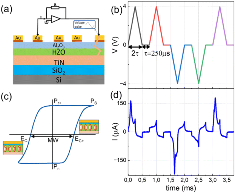 | ||
| Fig. 1 (a) Schematic diagram of the MFIM ferroelectric capacitor structure. Inset: triangular voltage sweep used in dynamic hysteresis measurements (DHMs). (b) An example of PUND voltage pulsing at 4 V used for ferroelectric hysteresis measurements. (c) A typical P–E loop with the key parameters for memory elements defined. (d) PUND current measured from S2 as an example. | ||
Structural characterization
Structural characterization of the samples was carried out by using the grazing incidence X-ray diffraction technique (GIXRD) on a Rigaku SmartLab diffractometer operating at 45 kV, 150 mA, with a Cu rotating anode. The incident angle ω was set at 0.35°, where the angle was at the half maximum reflectivity intensity. The ALD technique ensures the atomically flat surface. For our samples, this is confirmed by atomic force microscopy (AFM) with a root mean square roughness of around 0.5 nm.Electrical characterization
Electrical characterization of the samples was carried out by applying voltage between the bottom TiN and the top gold electrode. For ferroelectric polarization–electric field (P–E) hysteresis, endurance and retention measurements, a ferroelectric material tester AixACCT 2000E was used. Static current–voltage (I–V) characteristics were measured using a semiconductor parameter analyzer Keysight 1500A. Ferroelectric hysteresis was measured on 200 × 200 μm2 square junctions using both dynamic hysteresis measurement (DHM) and positive-up-negative-down (PUND) techniques with a triangle voltage sweep of 1 kHz. For endurance measurement, a rectangular voltage pulsing of 3 V, 100 kHz frequency was applied followed by 3 DHM measurements per decade to monitor the Pr value of the sample. All measurements were carried out at room temperature and under ambient conditions. C–f and G–f measurements were done using a Keysight semiconductor parameter analyzer B1500A at zero dc bias with the ac voltage amplitude of 250 mV and the frequency ranging from 1 kHz to 5 MHz.Results and discussion
Structural characterization
Fig. 1(a) shows the structures of the MFIM capacitors used in the experiment together with their electrical characterization setup and a typical FE polarization hysteresis curve (Fig. 1(c)). The MFIM capacitors were subjected to a voltage pulse sequence, as shown in Fig. 1(b), to generate a current output, as shown in Fig. 1(d). Voltage pulses were applied on the Ti/Au top electrode keeping the bottom TiN electrode grounded.
Fig. 2 shows the grazing incidence X-ray diffraction (GIXRD) patterns of S1, S2 and S3 and approximate analytical estimation of different phases in the samples. The full-range scan of 2θ from 10° to 80° is shown in ESI Fig. S1.† In Fig. 2(a–c), we focus on the diffraction peak at around 30° by performing a high-resolution scan around the peak. Previously, it has been reported that Zr-doped HfO2 can crystallize into monoclinic (m), orthorhombic (o), and tetragonal (t) phases5 depending on the annealing temperature14, in-plane tensile stress from the bottom electrode (BE), oxygen partial pressure16 and the capping electrode material.17,18 The formation of the o-phase leads to ferroelectricity while the t-phase favors antiferroelectricity in Zr-doped HfO2.5,19 As shown in Fig. 2, all our sample peaks match well with the HZO results reported in the literature,20 where the Bragg peak positions and shapes suggest the coexistence of monoclinic (m-phase, space group P21/c), tetragonal (t-phase, space group P42/nmc) and orthorhombic (o-phase, space group Pca21) phases. It is important to point out here that due to the symmetric line shape of the narrow-range scan between 28° and 34°, it is difficult to clearly separate the o and t phase contributions by GIXRD alone.12 However, a comparison of the phase ratio of the three samples, quantified by the same technique, can provide a fair estimation of the phase fractions due to different thermal treatments. To quantify the contribution of each phase to the final diffraction peak at around 30°, we fitted the curve by deconvolution of the Gaussian function with fixed peaks at 30.4°, 30.8°, and 31.6° that represent the o, t and m diffraction peaks of HZO, respectively.15 Calculation of the area under each curve shows that all the three samples have around 5% m-phase after RTA (Fig. 2(d)), confirming the negligible percentage of non-polar phase fraction in all samples. S2, which was annealed at 550 °C, shows a higher percentage of the o-phase compared to S1 and S3, while S1 (RTA at 450 °C) shows a higher percentage of the t-phase compared to S2 and S3. All three samples are polycrystalline mixed phases with S2 being o-phase dominant, S1 being t-phase dominant while S3 shows almost a similar amount of o and t-phases. Among all our samples, S2 has the smallest Bragg peak diffraction angle at 30.55° (Fig. 2(b)), suggesting a larger out-of-plane crystal size formed followed by S3 at 30.65°. This is expected considering the previous reports of higher orthorhombic phase formation due to higher annealing temperature.14,21 In our previous study,20 we found that the preferential growth of TiN along (200)c (cubic, space group Fm![[3 with combining macron]](https://www.rsc.org/images/entities/char_0033_0304.gif) m) can positively influence the growth of the HZO o-phase. A high amount of the polar phase in S1, S2 and S3 also supports this conclusion.
m) can positively influence the growth of the HZO o-phase. A high amount of the polar phase in S1, S2 and S3 also supports this conclusion.
 | ||
| Fig. 2 (a), (b) and (c) GIXRD 2θ scans in the range of 28°–34° over the predicted m (−111), o (111) and m (111) peak positions of S1, S2 and, S3 respectively. Peak fitting of the 2θ scans of S1, S2 and S3 with different reference diffraction peaks used to calculate the ratio of different crystalline phases. (d) Comparison of o-, t- and m-phases in the three samples. | ||
Polarization (P)–electric field (E) characteristics
Fig. 1(b) shows the positive-up-negative-down (PUND) pulse parameters used for ferroelectric hysteresis measurements (Fig. 1(c)) and Fig. 1(d) shows the corresponding dynamic current response of the capacitors. In ferroelectric materials, under an external electric field (E), a net switchable polarization appears that is retained even after the electric field is removed, giving rise to non-volatile retention of the polarization. With increasing E, the net polarization of the material increases due to more and more polarized domains aligning themselves in the direction of E. Beyond a critical field EC, the coercive field of the material, most of the polarized domains align in the direction of E. Therefore, for E > EC, the polarization starts to saturate at Ps and remains at a certain value at zero bias Pr, the remanent polarization. Similarly, when a negative bias is applied, polarization saturates at −Ps with a coercive field of −EC and remains at −Pr. This switchable polarization is used to store data in FE capacitors. Under an ideal situation of fully screened polarization charges, the devices can maintain a square like hysteresis. However, in practical devices with interfacial dead layer formation between the metal and the FE layer and other crystal defects, polarization loss happens, resulting in rounded hysteresis. Besides, in ultra-thin film capacitors, needed for nano-scale electronic components, a significant dielectric leakage current appears that affects the true estimation of the polarization charges and reduce device lifetime.Fig. 3(a), (b) and (c) show the dynamic current–voltage (I–V) loops and Fig. 3(d), (e), and (f) show the polarization–electric field (P–E) hysteresis of S1, S2 and S3 measured using the PUND technique. All data are from the pristine HZO capacitors without any wake-up cycling. For PUND measurements, we used triangular pulses of 1 kHz frequency and a voltage amplitude of up to ±4.6 V. Each PUND measurement sequence consists of one pre-poling pulse, read pulse and subsequently a rewrite pulse. In PUND, the first pulse of each pair contains all current contributions and the second pulse of the pair arises from the dielectric and leakage contribution of the device.22 The final P–E hysteresis was calculated by subtracting the current response from the second up pulse from the last positive voltage pulse since the first positive pulse has memory from the pre-poling, and the fourth down pulse from the third negative pulse. The polarization charges measured using PUND, thus, gives more accurate values of Ps and Pr.
 | ||
| Fig. 3 (a), (b) and (c) I–V plots and (d), (e) and (f) P–E plots for samples S1, S2 and S3, respectively. Measurements were performed with the PUND pulsing scheme with triangular pulses of 1 kHz frequency. | ||
S1, S2 and S3 show distinct differences in the displacement current features near the EC. While S1 shows a broad transition with double peaks as shown in Fig. 3(a), the transition for S2 and S3 is much sharper. This double peak feature becomes visible in the P–E loop as well where S1 shows a slightly distorted P–E hysteresis while that for S2 and S3 are rather sharp FE hysteresis. This separated switching current peaks might have different origins: (1) coexistence of tetragonal and orthorhombic phases in HZO with the tetragonal phase, leading to an antiferroelectric like double-peak switching19 or (2) the structural defect-rich sample where rapid domain rotation gets restricted due to the presence of a large number of domain pinning centers, leading to multiple ECs that become visible through multiple displacement current peaks or the coexistence of both. To verify the dominant process in our samples, we performed longer field cycling of the samples. The double peak features of S1 and S2 disappear after 107 and 106 cycles of pulsing, as shown in ESI Fig. S2(a and b),† respectively, with ±3 V square pulses of 100 kHz frequency, indicating field-induced crystallization from the t-phase to the o-phase of HZO happens in the samples that are annealed at lower temperature, as also previously observed by Lederer et al.19 However, even the 450 °C annealed samples do not show a pinched hysteresis in the pristine phase when measured with dynamic hysteresis measurements (DHMs), suggesting the t-phase not to be a dominating factor. The second factor, i.e., high density of structural defects, is a major contributor in S1 and partially in S2 which brings both advantages and challenges and have been discussed in later sections of the article.
For all three samples, the P–E loops were measured by varying the pulse amplitude from ±2 V to ±4.6 V, showing the possibility of multiple stable polarization states. Increasing voltage amplitude manifested an increasing switching current, leading to higher saturation and remanent polarization. Almost linear increase in Pr value in the range of 2.5–18 μC cm−2 was observed for S1 and S2 due to increasing pulse amplitude while for S3, a steeper rise in Pr value is obtained in the lower field regime followed by a saturating trend, as shown in ESI Fig. S3.† However, the Pr value is limited to 15 μC cm−2 for S3 since hard breakdown happens when the applied voltage is above 4 V, whereas S1 and S2 can endure until 4.6 V and 4.3 V, respectively, as shown in Fig. 3(a and b). Such a phenomenon is in line with the previous reports that with increasing annealing temperature, there is an increasing leakage contribution to the MFM device,21,23,24 which dominates the current flow at a higher electric field and shortens the device due to hard breakdown of the HZO layer. S1 and S2 show the highest Pr value of ∼18 μC cm−2 at 4.6 V and 4.3 V, respectively. This clearly indicates that due to RTA at 550 °C, higher fraction of HZO gets crystallized to the ferroelectric orthorhombic phase compared to S1 and S3, resulting in higher Pr and lower EC. Although S1, which was annealed at only 450 °C, is not fully crystallized to the o-phase, application of higher voltage can lead to a comparable Pr value since S1 can endure higher bias stress due to its lower crystallinity and oxygen vacancies.
The EC values for the positive and negative voltage sides of the P–E loops are different in all samples, showing the imprint effect of ferroelectric capacitors (Fig. 3). In FE capacitors, the imprint effect arises from dissimilar electrode configuration25 on either side of the FE, stress induced from electrode lattice mismatch17 or from asymmetric charge trapping at the ferroelectric electrode interface by defects.14 In the present experiments, a dielectric (DE) layer of Al2O3 was intentionally added in all the MFM devices. The choice of the Al2O3 capping layer was motivated by the fact that this ultrathin oxide ensures good ferroelectricity in HZO devices20 that were not annealed in the presence of a TiN top electrode, which was considered mandatory in earlier works. The choice of 1 nm thickness of the Al2O3 layer was motivated as a compromise between serving as a tunnel barrier to ensure stable ferroelectric switching18,26 and its contribution to the depolarization field consequently causing retention loss.22 The 1 nm dielectric layer at the top interface inhibits the down to up polarization rotation, leading to a higher value of EC− compared to EC+. Additionally, the change in EC due to different applied pulse amplitudes is more pronounced on the negative side, suggesting more restricted domain rotation from down to up direction resulting from trapped charge-related domain pinning sites at the HZO–Al2O3 interface. Due to the same composition of the capacitor stack, the imprint effect is supposed to show identical values in all samples. In reality, however, crystal structures, grain orientations and charged oxygen vacancies formed during RTA at different temperatures are different and subsequently pulsing experiments contributing to the formation of charge trapping and domain pinning sites also vary, leading to different performances of S1, S2, and S3 with S2 showing the least imprint and sharpest polarization switching.
Wafer-scale uniformity
For implementation of the devices in larger circuits and for cost-effective industry-scale production, it is important to have information on the wafer-scale uniformity of the device performance. It is previously found that fabrication process parameters affect the size of crystallites, thereby affecting the wafer-scale uniformity of the devices.27 In order to show the effect of RTA temperatures on the wafer-scale uniformity, in Fig. 4 we plotted the distribution of the Pr values for multiple devices from S1, S2 and S3 measured from different locations all over one-quarter of a wafer. Based on the position of the sample on the wafer, the Pr values can range from 2 to 15 μC cm−2 when measured with ±3 V DHM pulses of 1 kHz frequency, represented by the color scale. The measurement voltage was kept at 3 V so that the maximum number of devices can be measured without hard breakdown. The devices that are shorted during fabrication and measurement processes have been represented in black color. As a general observation, the edges of the wafers show a higher density of low-performance or shorted devices, likely caused by mechanical defects caused by wafer handling, non-uniformity of growth of the PEALD grown TiN bottom electrode and non-uniform thermal gradient during the RTA process. The hypothesis of a thermal gradient during RTA is derived from the fact that in all 3 samples, the center of the quarter showed most uniform device performance. From the color map, it becomes clear that Pr values range from 2.4 to 8.7 μC cm−2 for S1 and 3 to 15.2 μC cm−2 for S2. The highest number of devices shows Pr values of 6 μC cm−2 for S1 and 8 μC cm−2 for S2. The higher temperature annealed sample S3 is comparatively more uniform at the center of the sample with Pr values ranging from 5.9 to 12.9 μC cm−2 and a peak at around 11 μC cm−2 when the entire quarter of a wafer is considered. There exists certain degree of variation in all 3 samples. ESI Fig. S4† shows DHM from multiple devices of S1, S2 and S3 for a quick comparison. The contour plots in Fig. 4(a–c) confirm that lower temperature annealing contributes to a low Pr all over the wafer and narrower distribution of Pr values throughout the wafer. Higher temperature annealing, on the other hand, leads to a larger Pr value with higher variation of polarization values throughout the sample. Due to high leakage currents, more shorted junctions are found in S3. However, within 1 × 1 or 2 × 2 cm2 proximity in the middle of the wafer, it is possible to find a narrower distribution of device performance matrices in S3.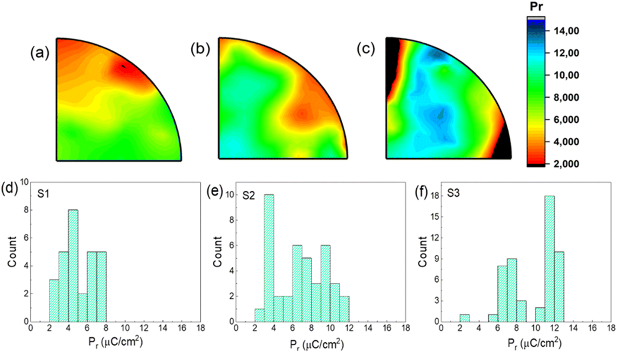 | ||
| Fig. 4 Mapping of the remanent polarization (Pr) values from the measured devices from one-quarter of a 150 mm wafer. All Pr values were measured using dynamic hysteresis measurement (DHM) with ±3 V, 1 kHz applied voltage. (a), (b) and (c) Contour plots showing the physical location of the high Pr and low Pr devices. (d), (e) and (f) Statistical distribution of the Pr data for samples S1, S2, S3, respectively. | ||
This trend of higher temperature annealed samples having higher Pr values agrees well with the GIXRD data and the previously reported trend11,14,21 that with increasing RTA temperature (until 800 °C24), the increased amount of the o-phase crystallized can lead to an increase of Pr values. However, from the uniformity point of view, S1 has a low standard deviation value of 1.7, which is lower than 2.8 for S2 and 2.5 for S3. S3, on the other hand, shows the highest number of devices with high Pr values around the center part of the sample, which leads to the possibility of densely packed high-performance circuit fabrication around this region. Low Pr samples around the edges of the wafers suggest incomplete crystallization around these areas that would require further investigation and process parameter optimization before a higher uniformity is reached.
Endurance characteristics
For neuromorphic computing tasks, such as online training, one important device parameter is the very high endurance of the synaptic devices since devices need to switch for more than 109 cycles to obtain the correct synaptic weight.28 To estimate the endurance properties of our devices, fatigue measurements on the 3 samples were performed with the following protocol.As shown in the inset image of Fig. 5(a), devices were pulsed with rectangular pulses of ±3 V, 100 kHz frequency. To investigate the evolution of FE hysteresis over several field cycles, every 1/3rd of a decade, one DHM measurement was performed with triangular pulses of ±3.5 V amplitude and 1 kHz frequency. S1 and S2 devices were able to endure long pulsing cycles exceeding 109 cycles (when DHM was measured at 3 V) with diminishing Pr and EC values. However, for S3, devices showed hard breakdown (HBD) after 4 × 10⁷ cycles, as shown in Fig. 5(a–c) with a trend of increasing Pr− and EC due to field cycling. A gradual fatigue behavior started setting in after almost 107 cycles in S1. In comparison, S2 started to show faster development of fatigue (after 106 cycles) under the same pulsing protocol. The 2Pr value (sum of Pr+ and Pr−) decayed to 63% of the pristine 2Pr at 2 × 10⁸ cycles for S1 and at 4 × 10⁷ cycles for S2, as shown in Fig. 5(c). At the end of the fatigue test for S2 (4 × 10⁸ cycles), 2Pr further decayed to 37%, in contrast, S1 remains at 55% of pristine 2Pr after the same number of cycles and was able to sustain further pulsing cycles exceeding 109.
 | ||
| Fig. 5 Endurance tests performed on the S1, S2 and S3 junctions showing evolution of (a) Pr (Pr+ and Pr−) and (b) coercive fields (EC+ and EC−) as a function of cycle number. (c) Normalized 2Pr values of S1, S2 and S3 in accordance with the fatigue cycle number. The inset of (a) shows the rectangular ±3 V, 100 kHz voltage pulsing scheme used for all fatigue tests. DHM measurements were performed (at each data point) with a triangular pulse of 3.5 V magnitude at 1 kHz frequency. (d–i) Pristine (blue) and after specific number of pulsing cycles fatigued (red for S1 and S2, and orange for S3) DHM: I–V hysteresis (d–f) and P–E hysteresis (g–i) showing a reduced Pr and narrowing memory window (MW) in S1 and S2. | ||
Fig. 5(d–i) show the dynamic I–V and P–E hysteresis before and after the fatigue tests. The dynamic I–V hysteresis (Fig. 5(d–f)) during the fatigue tests shows that with increasing number of field cycles, the leakage current contribution starts to increase, which is shown in Fig. 5(h and i), as a shift (narrowing for S1 and S2 is discussed later) of the P–E hysteresis towards the negative polarization direction caused by movement of oxygen vacancies under continuous bias stress. In all three cases, the leakage current starts to increase with increasing field cycles, mainly on the negative voltage side, confirming the role of positively charged oxygen vacancy migration under repeated field cycles and eventual conducting path formation to be one major contributing factor for leakage current in thin film HZO capacitors. It results in degradation of 2Pr and EC s in S1 and S2 while causing HBD in the S3 samples. HBD in S3 is most likely the result of filamentary path formation of oxygen vacancies that are strong enough not to get ruptured under opposite bias, causing a permanent conduction channel between the top and bottom electrodes.
It is observed in the evolution of DHMs of S1 and S2 in Fig. S4(a and b)† that the double peak feature merges into one switching current peak while shifting to the smaller voltage value followed by a degradation of switching current on both the positive and negative field sides, whereas S3 shows HBD before showing any significant degradation. The degradation is shown as a trend of constantly decreasing Pr+ and EC+ and a first increasing then decreasing EC− in S1 and S2 Fig. 5(g and h). Such a shift of switching current on the voltage axis and degradation of Pr and MW (sum of EC+ and EC−) upon continuous pulsing can be attributed to various effects that come into play during continuous bias stressing: (1) mixed-phase polycrystalline HZO (in this case S1 and S2) undergoes field-induced crystallization to the o-phase so that the external electric field needed to switch polarization is less than that of a pristine sample and (2) the reduced Pr and imprint phenomenon can be attributed to the asymmetric charge trapping by defects14 at the FE–DE interface in this study, HZO–TiOxNy (TiON) and HZO–Al2O3. The latter factor is discussed in section B and it is similar in all S1, S2, and S3 samples. Different endurance performances and fatigue mechanisms can therefore be attributed mainly to the former factor HZO–TiON interface and different amounts of oxygen vacancy formation due to different oxidation states of TiN caused by different RTA temperatures.
In the case of S3, only the visible fatigue mechanism is imprint, which is shown as continuously increasing EC+ and EC− values in Fig. 5(i) and no degradation of 2Pr and MW narrowing happens until the breakdown, as also can be seen from Fig. 5(a–c). Moreover, hard breakdown appeared before the development of severe fatigue (degradation of Pr+). This is in line with the data in Fig. 3(c and f), where S3 was unable to handle larger PUND pulse amplitudes, indicating larger leakage current in the high temperature annealed samples. With increasing pulse amplitude in fatigue measurements, devices started showing increased fatigue and could not sustain a high number of field cycles. For S3, the P–E loop starts shifting on the voltage axis upon repeated field cycles, showing an increased imprint effect arising from the internal electric field induced by charged defect generation and movement during field cycling.29,30
Leakage current – effect of the microstructure and interface
The I–V and P–E data in Fig. 3 are the results from PUND measurements where the leakage current components are subtracted from the total current to correctly estimate the displacement current component. In real applications, however, the leakage component from the ultra-thin capacitors cannot be subtracted and therefore is a critical parameter that needs to be considered while evaluating device performance. As seen from the GIXRD data (Fig. 2) and the dynamic I–V measurements (Fig. 3), with increasing annealing temperature, the ferroelectric orthorhombic phase increases. From the static current–voltage measurements (Fig. S5†), we found that the static current of sample S2 is almost an order of magnitude higher compared to S1 at 2 V bias and almost 2 orders of magnitude higher for smaller bias. As discussed previously, it has been found previously that low temperature annealing leads to a semi-crystalline phase19 in HZO with the formation of less oxygen vacancies.11 The presence of the amorphous phase leads to reduced leakage current paths and reduced oxygen vacancy formation causes less trap-assisted tunnelling. Both effects contribute to the decreased leakage current density in sample S1. The higher crystallinity of HZO leads to more randomly oriented grains and grain boundaries that results in a higher amount of leakage current paths through the device, resulting in quicker fatigue and breakdown compared to devices with lower polarization values with a more amorphous oxide phase. S3 shows almost similar leakage current at higher voltage to S2, however a lower leakage in the low bias range.To investigate the role of the TiN–FE interface in modifying the leakage currents, we prepared another sample, S4, based on the same fabrication procedure of S1; however, in S4, TiN was intentionally placed in air for 7 days before HZO growth. This intentional oxidation of TiN into TiON gave us the opportunity to investigate the effect of having an oxygen reservoir layer at the HZO–bottom electrode interface that could modify the vacancy formation, affecting the leakage currents in return. Fig. 6 shows the I–V and P–V characteristics of sample S4, showing a higher switching voltage on the positive voltage side (Fig. 6(a)) and a much higher Pr of 33 μC cm−2 (Fig. 6(b)) in the sample due to the ability of S4 to withstand a bias stress of ±6 V. In comparison to S1, the devices showed identical −EC values but increased +EC values, suggesting a significant voltage drop (of ∼2 V) across the bottom TiON layer. Most importantly, the leakage current in S4 decreased significantly compared to S1 and S3 in the quasi-static range (Fig. 6(d)). The static I–V data in Fig. S5† asserted this further by showing almost 3 orders of magnitude less leakage current in S4 in comparison to S2 and S3 and more than 2 orders of magnitude for S1 at 3 V. This reduced leakage current can be attributed to the formation of less oxygen vacancies during the RTA step in the presence of an oxygen reservoir layer at the bottom interface and additional non-polar barrier formation preventing trap-assisted tunneling. This reduced leakage current resulted in a long device lifetime; however, a large fatigue started to settle in after 105 cycles of operation (Fig. 6(e)). This fatigue, however, is found to be recoverable with a few DHM cycles with a slightly higher voltage amplitude compared to the pulsing voltage amplitude. The mechanism of fatigue in various kinds of thin film ferroelectric devices and recovery from fatigue throws light on the interplay of charge trapping at the FE–DE interface and the role of oxygen vacancies and can act as an important guideline in designing next-generation non-volatile memory devices. In the next section, we discuss this phenomenon in detail.
 | ||
| Fig. 6 FE characteristics of S4: I–V hysteresis (a) and P–E hysteresis (b) measured with DHM at 1 kHz with various voltage amplitudes showing the that devices have a larger memory window and can withstand large electric fields of 6 MV cm−1, giving a high 2Pr value of 66 μC cm−2. (c) Comparison between S1 and S4: I–V plots measured with PUND showing a shift in the positive voltage peak due to the presence of an oxide layer at the bottom electrode. (d) Low-frequency leakage currents with samples S1 and S3, showing that leakage is significantly reduced in S4. (e) I–V plots for monitoring DHMs (5 V, 1 kHz) during the fatigue measurement (rectangular ±3 V, 100 kHz voltage pulsing) up to 108 cycles. (f) DHMs measured before pulsing (black lines), after 107 cycles of pulsing (red lines), and after recovery (blue lines) with high voltage amplitude DHMs. | ||
Recovery from fatigue: role of defects, charge trapping and de-trapping
Wake-up of HZO devices is reported to be an inevitable step in many of the previous works.11,14,23 Similarly, a “re-wakeup” or recovery from fatigue using higher field pulsing29–32 has been also discussed in some recent works. In a TiN/HZO/TiN capacitor, recovery was achieved by 104 cycles of fatigue pulsing at 5 V,29 in a 1 T1C FeRAM capacitor, recovery was achieved by 108 cycles at 40% higher pulsing magnitude33 and in an Ru/HZO/Ru capacitor, recovery was achieved by 102 cycles of twice the pulsing field magnitude.30 In an HZO-based MFIS–FeFET structure,34 an ultrafast recovery by 1 cycle of a unipolar voltage is shown that can enable a prolonged endurance. This result, when compared to the MFM stacks, gives the insight that based on the stack design, the presence of a dielectric can bring quicker recovery. In this work, we designed a protocol which can achieve recovery from fatigue within 5 sweeping cycles with only 20% higher field magnitude (4 V) of pristine pulse (3.5 V), as shown in schematic Fig. 7(d). A comparison of the FE characteristics and recovery in capacitor and FeFET device stacks is presented in Table 1. | ||
| Fig. 7 Recovery from fatigue measurements performed on the S1 (a), S2 (b), and S4 (c) junctions showing evolution of Pr as a function of cycle number. Monitoring DHM was carried out at 3.5 V, 1 kHz for S1 and S2 and at 5 V, 1 kHz for S4 at each data point. (d) Pulsing schemes employed for fatigue and recovery measurements. Magnitude of the recovery pulses are shown by the color code. (e) Normalized 2Pr values of S1, S2 and S4 as a function of fatigue cycle numbers after 1st, 2nd, and 3rd recoveries showing that the same Pr states can be achieved reproducibly after each fatigue and recovery cycle. | ||
| Device architecture (BE/HZO/TE) | Annealing temperature (°C) | Applied electric field (MV cm−1) | P r (μC cm−2) | MW 2Ec (MV cm−1) | Endurance (cycles) | CMOS BEOL compatible | Recovery technique | Recover y(2Pr/2Pr Pristine) | Ref. |
|---|---|---|---|---|---|---|---|---|---|
| W/HZO/W/Pt | 700 PMA 60 s | 4@111 kHz (after 102 cycles) | 32 | 4 | 108 (111 kHz) | No | — | — | 11 |
| TiN/HZO/Al2O3/TIN | 400 PDA 30 s | 3.89@1 kHz | 15.3 | 4 | — | Yes | — | — | 18 |
| TiN/HZO/Al2O3/Au | 500 PDA 30 s | 5@500 kHz | 30 | 6.2 | 104 (100 kHz) | Yes | — | — | 20 |
| 3@500 kHz | 12.5 | — | 106 (100 kHz) | ||||||
| TiN/HZO/TiN | 600 PMA 30 s | 3@1 kHz (after 105 cycles) | 19.1 | 1.97 | 1.6 × 10⁷ (10 kHz) | No | — | — | 14 |
| TiN/ZrO2/HfO2 (superlattice)/TiN | 600 PMA | 3 (after 104 cycles) | 15 | 3 | 1011 (1 MHz) | No | — | — | 23 |
| TiN/HZO/WNX/Ru | 400 PMA 1 h | 2@1 kHz | 12.5 | 3 | >1010 (1–2 MHz) | Yes | 103 pulses ±3 MV cm−1, 100 Hz | 82% | 32 |
| TiN/HZO/TiN (MFM) 1 T1C-FeRam | 600 PMA | 3.5@1 kHz | 12 | 2.5 | >108 (5 MHz) | No | 108 pulses with ±4 MV cm−1, 5 kHz | 140% | 33 |
| Si/IL/HZO/TiN (MFIS) FeFET | 600 PMA 30 s | — | — | 1.5 | >108 (5 MHz) | No | 1 nonpolar pulses 4.4 MV cm−1, 5 kHz | — | 34 |
| TiN/HZO/Al2O3/Ti/Au | 450 PDA 30 s | 4@1 kHz | 15 | <3 | >109 (5 MHz) | Yes | 10 pulses ±4 MV cm−1, 1 kHz | 88% | This work |
| TiN/TiNOX/HZO/Al2O3/Ti/Au | 450 PDA 30 s | 5@1 kHz | 22 | <5 | >108 (5 MHz) | Yes | 10 pulses ±5.5 MV cm−1, 1 kHz | 93% | This work |
Fig. 7 shows the fatigue of Pr over pulsing cycles and their recovery trends in S1, S2 and S4 devices. It is found for all devices, recovery from the fatigued Pr values is possible by applying a higher external electric field sweep with a custom protocol. For the recovery characterization, fatigue measurement (FM) was carried out the same way as shown in Endurance characteristics chapter with intermediate gaps while fatigued states set in and applying several DHM pulsing cycles at certain voltage amplitude for recovery. The 2Pr value of S1, as shown in Fig. 7(a), decayed to 11.8 μC cm−2 after the first 108 fatigue pulsing cycles. The recovery was carried out by applying dynamic hysteresis measurements up to 10 times, which consist of triangle voltage sweep at 1 kHz with a higher voltage amplitude (in the cases of S1 ± 3.6 V, ±3.7 V, and ±3.8 V) compared to the pulsing voltage amplitude. After 3 DHM cycles, recovery from the fatigue state was obtained with Pr+ of S1 fully recovered, whereas Pr− is only 70% recovered, as shown in Fig. 7(a). The recovery of S2 was performed in the same way using DHMs with ±3.7 V, ±3.8 V, and ±4 V after 107 pulsing cycles. Similar to S1, after 3 DHM cycles, recovery from the fatigue state was obtained with Pr+ of S2 recovering 96% compared to 79% of Pr−, as shown in Fig. 7(b). The loss of S1 and S2 from fatigue test, which cannot be recovered, is the result of the charge carriers trapped in HZO–Al2O3 interfaces those are unable to respond to the applied recovery pulse sequences and prevent a full or higher percentage of recovery (Fig. 8).
 | ||
| Fig. 8 Capacitance vs. frequency (C–f) plots for samples (a) S1, (b) S2 and (c) S4 in the pristine and fatigued states. Schematic diagram of (d) the generation of different defect states and charge trapping and (e) the domain pinning mechanism in the S1 and S4 samples in pristine and fatigued states. | ||
Since the MW for S4 is larger (as shown in Fig. 6), a voltage amplitude of ±5 V was applied for monitoring fatigue and recovery of S4. Recovery DHMs with ±5.5 V and ±5.7 V were applied after 107 voltage pulses in S4. As shown in Fig. 7(c), the devices show a quicker set in of fatigue meanwhile a better recovery of 93% of pristine values on both up and downside of remanent polarization. As discussed in Endurance characteristics chapter, S2 decays relatively faster than S1, which is in line with the data in Fig. 7(e). Nevertheless, after the recovery, the fatigue of all samples seems to have their pristine states nearly back and many longer pulsing cycles can be achieved.
Recovery from fatigue in HZO devices have been reported previously.29–32 However, a microstructure and interface dependence of the effect and physical interpretation of the process is still missing. Here, we analyze the fatigue and recovery in our samples through device modelling and trap density calculations and provide a guideline for the improvement of fatigue and recovery processes through material and stack engineering.
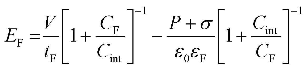
The effective electric field across the ferroelectric layer in an MFIM capacitor, EF, is given as:
 | (1) |
For a clearer understanding of the effect of interface trap densities on the observed fatigue and recovery behavior, we measured capacitance as a function of frequency (C–f) at zero dc bias for S1, S2 and S4, both in their pristine and fatigued states (Fig. 8(a)–(c)). Interface trap density (Dit) can be calculated from the frequency dispersion of the capacitance.35 At low frequencies, all traps can follow the AC signal. At higher frequencies, interface traps cannot follow the AC signal and therefore the difference in capacitance at low and high frequencies gives a fairly good estimation of the interface trap states. In our experiments, the capacitance of the pristine device begins to deteriorate at 100 kHz for S1, at 10 kHz for S2, and at 7 kHz for S4. The relaxation/resonance peak of HZO for S1 and S2 appears at approximately 1 MHz, with the peak in S2 being broader, suggesting a distribution of trap energies with increased thermal energy due to higher annealing temperature allows more traps to be activated. For sample S1, we found a slight change in the zero bias capacitance value between the pristine and fatigued samples in the frequency range of 1–10 kHz, while for S2, the change in capacitance is minimal. For S4, in the measured frequency range, the capacitance values decreased slightly from the pristine sample to the fatigued sample. This trend, together with the fatigue and recovery data, throws light on the underlying mechanism for the nature of charge trapping in the samples with a single or double DE oxide interface. From the analysis of the leakage, capacitance and fatigue and recovery data, we then come to a unified picture that is schematically shown in Fig. 8(d) and (e). In S1, S2 and S3, oxygen vacancies are formed during the RTA step as the TiN scavenges oxygen from the HZO layer, leading to a high density of vacancy-related defects in the HZO layer. In comparison, much less vacancies are formed in S4 due to the thicker oxide layer at the bottom interface supplying oxygen to the TiN. During field cycling, S1 and S2 get a high amount of charged vacancies distributed throughout the HZO layer that causes charge trapping centers and pinning FE domains at these traps. In S4, interface defect-related traps exceed the vacancy-related traps due to the presence of two FE and DE interface layers that causes domain pinning. Interface traps, reflected by the C–f measurements, causes quicker fatigue due to charge trapping but higher recovery due to de-trapping under higher applied bias. The Dit value calculated from the C–f data shows interface trap density for S1 and S2 in the range of 4–5 × 1013 cm−2 eV−1 that is in the similar range as reported by Qu et al.36 for the 10 nm HZO/1–3 nm Al2O3 layer using the conductance method. The numbers for S4 are in the same range; however, due to the unknown thickness and dielectric constant of the TiON layer, this estimation poses certain ambiguity. Therefore, we also verified the Dit values with conductance method. The frequency response of trap states depends on the trap time constant and maximum loss occurs when interface traps are in resonance with the applied ac signal (ωτ = 1). Assuming that surface potential fluctuations can be neglected, Dit can be estimated from the normalized parallel conductance peak, (Gp/ω)max, as shown by Engel-Herbert et al.35 . From the calculations done from our measured G–f data (not shown here), we found the Dit value to be in the range of 2 × 1013 cm−2 eV−1 that matches excellently with the values estimated from the C–f data. The frequency dependence of trap states, however, is found to be different in the samples for pristine and fatigued states that could provide a valuable design principle for the high-endurance memory devices. More in-depth characterization and modelling of charge trapping and de-trapping in these samples are currently underway.
Modelling the fatigued and recovered polarization hysteresis
For a better physical understanding of the impact of fatigue on the circuit-level performance, the effect of fatigue and subsequent recovery was evaluated through SPICE and Verilog A compatible Jiles–Atherton (JA) model.37 The JA model is a domain wall kinetics-based model capable of simulating asymmetric ferroelectric polarization with physical interpretations including domain wall pinning and depinning.38The ferroelectric polarization is solved simultaneously with leakage and a linear permittivity to fully represent the measured DHM data. The simulated pristine, fatigued and recovered curves for the S4 sample are presented in Fig. 9, assuming movement of domain walls is the main contributor to the current peaks. For S1 and S2, where the fatigue cycling does not diminish current peaks in the dynamic hysteresis measurement, the fatigue and recovery of the samples cannot fully be explained only by the domain wall kinetics of the ferroelectric. So, additional non-ferroelectric current contributions, such as conduction channels due to increased oxygen vacancies, need to be included in the model to reliably simulate device performance. The dynamic modulation of domain wall kinetics parameters, leakage and dielectric contribution with bias stress due to pulse cycling is a complicated process with multiple interdependent parameters and the fatigued states in these samples were difficult to model following a model with ferroelectric contribution together with a parallel linear dielectric contribution. Due to the decreased number of oxygen vacancies in the S4 sample that led to reduced leakage, simulating the operation with only domain wall kinetics was possible, unlike in the S1 and S2 samples. It was found that in the fatigued states, the FE contribution to the total current is visibly reduced, pointing to the fact that in the fatigued states, FE domains are severely pinned, however, can be de-pinned with larger applied voltage pulses. For a circuit level operation, it is important to find out the point where devices are no longer showing FE switching and need recovery. Future work in this direction is underway to model the device fatigue and recovery in the presence of high leakage currents.
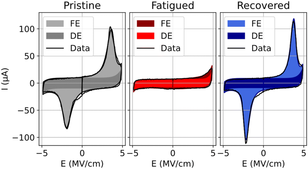 | ||
| Fig. 9 Dynamic I–V curves simulated using a JA model for the ferroelectric contribution together with a parallel linear dielectric contribution including an exponential leakage for sample S4 and validated with the experimental DHM data for pristine, fatigued and recovered states. | ||
Application in memory and neuromorphic hardware
This result has significant implication for fabrication of densely packed 1T-1C FeRAM, 1 T FeFET or capacitive memory arrays. In the semiconductor industry, dynamic random-access memory devices (DRAM) or static random-access memory devices (SRAM) are the most used memory devices as volatile memory devices while NAND flash is most used as non-volatile memory. DRAMs and SRAMs operate with lower voltages, showing fast read/write operations, however, with fast data loss that requires frequent refreshing of the memory. Flash memory devices operate at a higher voltage that restricts the device lifetime to 105 cycles of operation. FE capacitor-based FeRAMs can combine the best of both worlds by performing fast read/write operations, non-volatile data retention and long device lifetime. Our current observation provides a design clue for high-performance non-volatile memory and neuromorphic circuits. While high Pr values, lower switching voltage, and fast switching times are the more desirable parameters for digital non-volatile memory components, for neuromorphic circuits, requirements are more analog states, reproducibility of switching to multi-level conductance and endurance exceeding 109 cycles for online training while for inference tasks a long data retention time is essential. Our results suggest, by low temperature crystallization of the ferroelectric layer, that it is possible to design BEOL-integrated 1T-1C FeRAMs with multibit operation, high endurance and recoverable fatigue that makes them suitable for online training works in neuromorphic circuits.In our previous studies with single-crystalline perovskite oxide BaTiO3- and Pb1−xZrxTiO3 (PZT)-based FTJs, the vital role of oxygen vacancy migration in ultrathin FE films was investigated that gave rise to large resistive switching.39,40 For polycrystalline polymer ferroelectric FTJs, it was found that through modification of the microcrystalline structure of the ferroelectric, it is possible to have ultrafast switching (<20 ns) and controllable domain dynamics41 that can result in efficient online training for a multilayer perception-based neural network.42,43 Besides non-volatile memory functions, proper engineering of the depolarizing field at the ferroelectric–electrode interface can lead to control of the polarization relaxation in such a way that a programmable synaptic plasticity time constant44 or leaky integrate-and-fire (LIF) functions can be achieved45 using the same ferroelectric device that can significantly reduce the fabrication process complexity and cost of the fully-connected neural network. For HZO, multibit operation with varying voltage amplitude, shown in this work and in ref. 20, leads the way for designing analog FE memory arrays. A crossbar array of ferroelectric capacitors, FTJs or FeFETs can serve as the analog compute core, performing the vector matrix multiplication (VMM) operation by utilizing the Ohm's law and Kirchoff's current law, leading to efficient parallel weight updates that significantly improve the energy efficiency and latency of AI computation.3,4 In a crossbar array of analog memory components, doing an efficient multiplication operation requires a large number of conductance states achievable almost linearly with the change of voltage, current or time. In practical FE devices, achieving extremely high bit precision with significant linearity remained a challenge. By proper control of ferroelectric domain rotation,41 designing a custom-gate stack or by utilizing hybrid CMOS–FE synaptic cells, it is possible to achieve a high number of intermediate conductance states, leading to more than 96% simulated accuracy43 on classification tasks performed on the MNIST handwritten dataset. In simulation, however, we made a simplified assumption that devices at each cross point are identical. For designing a full-hardware implementation, device to device variation, leakage and fatigue issues needs to be considered as well. While high FE polarization is essential for opening a significant memory window, high leakage current results in a significant static power loss, increasing the power consumption and heating of the circuit. A leaky capacitor in an FeFET gate stack increases the gate leakage current, lowering the input impedance of the FeFET. Higher off-state current in an array could cause write or read disturbance to the nearby memory cells. For a 1T-1C FeRAM-based synaptic circuit, there will be charge leakage that will lead to loss of data and need of frequent refreshing of the capacitor. Additionally, high gate leakage leads to earlier fatigue and breakdown of the FeFET that has catastrophic consequences of hardware failure. The current work suggests that the less leakage path through ferroelectrics and less vacancy formation through low temperature annealing can lead to almost unlimited write endurance in BEOL ferroelectric analog memory and synaptic devices. A proper in-operando defect characterization and modelling is essential for a more accurate prediction of large-scale circuit implementation.
Conclusions
In conclusion, microcrystalline structure and interface engineering for ferroelectric HZO capacitor devices is presented in this work. It is found that low thermal budget annealed samples possess high endurance performance exceeding 109 cycles, however with a visible fatigue with increasing field cycles arising from oxygen vacancy redistribution-related leakage currents. By minimizing the oxygen vacancy defects, devices grown and annealed with the same parameters show improvements in Pr and leakage currents, however, with earlier set in of fatigue. Both kinds of fatigue could be recovered up to 90% multiple times in our devices with a few pulse cycling that provides an opportunity of runtime fatigue recovery in NVM components. Our results show that proper designing of stack and nanofabrication conditions can lead to CMOS BEOL compatible ferroelectric components with a low fabrication cost, a low operating cost and a long work time. Future experiments on the optimized FE–DE stacks, innovative device architectures and their large-scale integration will unravel the true potential of the technology.Author contributions
Xinye Li and Padma Srivari fabricated the samples, did structural and electrical characterization and data analysis, and contributed to the manuscript writing. Ella Paasio developed the device model, did the model validation of the experimental results and wrote the corresponding section of the manuscript. Sayani Majumdar planned the experiments, supervised the work, acquired funding and wrote the manuscript together with XL, PS and EP. All authors agreed with the final version of the manuscript.Data availability
The data supporting the conclusions of this article are available upon reasonable request from the corresponding author. Most of the experimental data have been included in the main text and as part of the ESI.†Conflicts of interest
There are no conflicts to declare.Acknowledgements
The authors acknowledge the financial support from the Research Council of Finland through projects IntelliSense (no. 345068), AI4AI (no. 350667), Ferrari (no. 359047), Business Finland and the European Commission through Chips JU project ARCTIC (Project #101139908). This work used experimental facilities of OtaNano Micronova cleanroom and the Research Council of Finland Infrastructure “Printed Intelligence Infrastructure” (PII-FIRI, project no. 358618).References
- D. S. Jeong and C. S. Hwang, Adv. Mater., 2018, 30, 1704729 CrossRef PubMed.
- I. Chakraborty, A. Jaiswal, A. K. Saha, S. K. Gupta and K. Roy, Appl. Phys. Rev., 2020, 7, 021308 CAS.
- A. I. Khan, A. Keshavarzi and S. Datta, Nat. Electron., 2020, 3, 588–597 CrossRef.
- S. Majumdar, Adv. Intell. Syst., 2022, 4, 2100175 CrossRef.
- J. Müller, T. S. Böscke, U. Schröder, S. Mueller, D. Bräuhaus, U. Böttger, L. Frey and T. Mikolajick, Nano Lett., 2012, 12, 4318 CrossRef PubMed.
- J. Okuno, T. Kunihiro, K. Konishi, H. Maemura, Y. Shuto, F. Sugaya, M. Materano, T. Ali, M. Lederer, K. Kuehnel, K. Seidel, U. Schroeder, T. Mikolajick, M. Tsukamoto and T. Umebayashi, in 2021 IEEE International Memory Workshop (IMW), 2021, pp. 1–3 Search PubMed.
- S. George, K. Ma, A. Aziz, X. Li, A. Khan, S. Salahuddin, M.-F. Chang, S. Datta, J. Sampson, S. Gupta and V. Narayanan, in 2016 53nd ACM/EDAC/IEEE Design Automation Conference (DAC), 2016, pp. 1–6 Search PubMed.
- L. Chen, T.-Y. Wang, Y.-W. Dai, M.-Y. Cha, H. Zhu, Q.-Q. Sun, S.-J. Ding, P. Zhou, L. Chua and D. W. Zhang, Nanoscale, 2018, 10, 15826–15833 RSC.
- S. Majumdar, Frontal Nanotechnol., 2024, 6 DOI:10.3389/fnano.2024.1371386.
- J. Hur, Y.-C. Luo, Z. Wang, S. Lombardo, A. I. Khan and S. Yu, IEEE J. Explor. Solid-State Comput. Devices Circuits., 2021, 7, 168–174 Search PubMed.
- S. Asapu, J. N. Pagaduan, Y. Zhuo, T. Moon, R. Midya, D. Gao, J. Lee, Q. Wu, M. Barnell, S. Ganguli, R. Katsumata, Y. Chen, Q. Xia and J. J. Yang, Front. Mater., 2022, 9, 969188 CrossRef.
- S. S. Cheema, D. Kwon, N. Shanker, R. dos Reis, S.-L. Hsu, J. Xiao, H. Zhang, R. Wagner, A. Datar, M. R. McCarter, C. R. Serrao, A. K. Yadav, G. Karbasian, C.-H. Hsu, A. J. Tan, L.-C. Wang, V. Thakare, X. Zhang, A. Mehta, E. Karapetrova, R. V. Chopdekar, P. Shafer, E. Arenholz, C. Hu, R. Proksch, R. Ramesh, J. Ciston and S. Salahuddin, Nature, 2020, 580, 478–482 CrossRef CAS PubMed.
- G.-H. Chen, Y.-R. Chen, Z. Zhao, J.-Y. Lee, Y.-W. Chen, Y. Xing, R. Dobhal and C. W. Liu, IEEE J. Electron Devices Soc., 2023, 11, 752–758 CAS.
- H.-G. Kim, D.-H. Hong, J.-H. Yoo and H.-C. Lee, Nanomaterials, 2022, 12, 548 CrossRef CAS PubMed.
- M. Hyuk Park, H. Joon Kim, Y. Jin Kim, W. Lee, T. Moon and C. Seong Hwang, Appl. Phys. Lett., 2013, 102, 242905 CrossRef.
- R. Taehyun, D.-H. Min and S.-M. Yoon, J. Appl. Phys., 2020, 128, 074102 CrossRef.
- S. J. Kim, D. Narayan, J.-G. Lee, J. Mohan, J. S. Lee, J. Lee, H. S. Kim, Y.-C. Byun, A. T. Lucero, C. D. Young, S. R. Summerfelt, T. San, L. Colombo and J. Kim, Appl. Phys. Lett., 2017, 111, 242901 CrossRef.
- C. Ju, B. Zeng, Z. Luo, Z. Yang, P. Hao, L. Liao, Q. Yang, Q. Peng, S. Zheng, Y. Zhou and M. Liao, J. Mater., 2024, 10, 277–284 Search PubMed.
- M. Lederer, D. Lehninger, T. Ali and T. Kämpfe, Phys. Status Solidi RRL, 2022, 16 DOI:10.1002/pssr.202200168.
- H. Bohuslavskyi, K. Grigoras, M. Ribeiro, M. Prunnila and S. Majumdar, Adv. Electron. Mater., 2024, 10, 2300879 CrossRef CAS.
- A. Kashir, H. Kim, S. Oh and H. Hwang, ACS Appl. Electron. Mater., 2021, 3, 629–638 CrossRef CAS.
- S. Lancaster, P. D. Lomenzo, M. Engl, B. Xu, T. Mikolajick, U. Schroeder and S. Slesazeck, Frontal Nanotechnol., 2022, 4 DOI:10.3389/fnano.2022.939822.
- Y.-K. Liang, W.-L. Li, Y.-J. Wang, L.-C. Peng, C.-C. Lu, H.-Y. Huang, S. H. Yeong, Y.-M. Lin, Y.-H. Chu, E. Yi-Chang and C.-H. Lin, IEEE Electron Device Lett., 2022, 43, 1451–1454 CAS.
- S. Migita, H. Ota, K. Shibuya, H. Yamada, A. Sawa, T. Matsukawa and A. Toriumi, Jpn. J. Appl. Phys., 2019, 58, SBBA07 CrossRef CAS.
- M. Pešić, T. Li, V. Di Lecce, M. Hoffmann, M. Materano, C. Richter, B. Max, S. Slesazeck, U. Schroeder, L. Larcher and T. Mikolajick, IEEE J. Electron Devices Soc., 2018, 6, 1019–1025 Search PubMed.
- B. Max, M. Hoffmann, S. Slesazeck and T. Mikolajick, in 2018 48th European Solid-State Device Research Conference (ESSDERC), 2018, pp. 142–145 Search PubMed.
- S. De, B.-H. Qiu, W.-X. Bu, M. A. Baig, P.-J. Sung, C.-J. Su, Y.-J. Lee and D. D. Lu, ACS Appl. Electron. Mater., 2021, 3, 619–628 CrossRef CAS.
- A. Mehonic, A. Sebastian, B. Rajendran, O. Simeone, E. Vasilaki and A. J. Kenyon, Adv. Intell. Syst., 2020, 2, 2000085 CrossRef.
- T. Gong, J. Li, H. Yu, Y. Xu, P. Jiang, Y. Wang, P. Yuan, Y. Wang, Y. Chen, Y. Ding, Y. Yang, Y. Wang, B. Chen and Q. Luo, IEEE Electron Device Lett., 2021, 42, 1288–1290 CAS.
- P. J. Liao, Y.-K. Chang, Y.-H. Lee, Y. M. Lin, S. H. Yeong, R. L. Hwang, V. Hou, C. H. Nien, R. Lu and C. T. Lin, Characterization of Fatigue and Its Recovery Behavior in Ferroelectric HfZrO, 2021 Search PubMed.
- Y. Cheng, Z. Gao, K. H. Ye, H. W. Park, Y. Zheng, Y. Zheng, J. Gao, M. H. Park, J.-H. Choi, K.-H. Xue, C. S. Hwang and H. Lyu, Nat. Commun., 2022, 13, 645 CrossRef CAS PubMed.
- A. Aich, A. Senapati, Z.-F. Lou, Y.-P. Chen, S.-Y. Huang, S. Maikap, M.-H. Lee and C. W. Liu, Adv. Mater. Interfaces, 2024, 2400185 CrossRef CAS.
- J. Okuno, T. Yonai, T. Kunihiro, Y. Shuto, R. Alcala, M. Lederer, K. Seidel, T. Mikolajick, U. Schroeder, M. Tsukamoto and T. Umebayashi, IEEE J. Electron Devices Soc., 2022, 1–1 Search PubMed.
- C.-H. Wu, J. Liu, X.-T. Zheng, Y.-M. Tseng, M. Kobayashi, V. P.-H. Hu and C.-J. Su, in 2023 International Electron Devices Meeting (IEDM), 2023, pp. 1–4 Search PubMed.
- R. Engel-Herbert, Y. Hwang and S. Stemmer, J. Appl. Phys., 2010, 108, 124101 CrossRef.
- Y. Qu, J. Li, M. Si, X. Lyu and P. D. Ye, IEEE Trans. Electron Devices, 2020, 67, 5315–5321 CAS.
- D. C. Jiles and D. L. Atherton, J. Appl. Phys., 1984, 55, 2115–2120 CrossRef CAS.
- E. Paasio, M. Prunnila and S. Majumdar, in 2023 IEEE 12th Non-Volatile Memory Systems and Applications Symposium (NVMSA), 2023, pp. 1–2 Search PubMed.
- Q. H. Qin, L. Äkäslompolo, N. Tuomisto, L. Yao, S. Majumdar, J. Vijayakumar, A. Casiraghi, S. Inkinen, B. Chen, A. Zugarramurdi, M. Puska and S. van Dijken, Adv. Mater., 2016, 28, 6852–6859 CrossRef CAS PubMed.
- H. Tan, S. Majumdar, Q. Qin, J. Lahtinen and S. van Dijken, Adv. Intell. Syst., 2019, 1, 1900036 CrossRef.
- S. Majumdar, Nanoscale, 2021, 13, 11270–11278 RSC.
- S. Majumdar, Neuromorphic Comput. Eng., 2022, 2, 041001 CrossRef.
- S. Majumdar and I. Zeimpekis, Adv. Intell. Syst., 2023, 5, 2300391 CrossRef.
- S. Majumdar, H. Tan, I. Pande and S. van Dijken, APL Mater., 2019, 7, 091114 CrossRef.
- S. Majumdar, H. Tan, Q. H. Qin and S. van Dijken, Adv. Electron. Mater., 2019, 5, 1800795 CrossRef.
Footnote |
| † Electronic supplementary information (ESI) available. See DOI: https://doi.org/10.1039/d4nr04861j |
| This journal is © The Royal Society of Chemistry 2025 |