
 Open Access Article
 This Open Access Article is licensed under a
 Creative Commons Attribution 3.0 Unported Licence
Coupled 2D quantum dot films for next generation solar cells: electronic structure and anomalous light absorption behaviour†
Rebeca V. H.
Hahn
 a,
Marco
Califano
b,
Salvador
Rodríguez-Bolívar
a and
Francisco M.
Gómez-Campos
*a
a,
Marco
Califano
b,
Salvador
Rodríguez-Bolívar
a and
Francisco M.
Gómez-Campos
*a
aDepartamento de Electrónica y Tecnología de Computadores, Facultad de Ciencias, Universidad de Granada, 18071, Granada, Spain. E-mail: fmgomez@ugr.es
bPollard Institute, School of Electronic and Electrical Engineering, University of Leeds, LS2 9JT, UK. E-mail: m.califano@leeds.ac.uk
First published on 3rd April 2025
Abstract
There is an increasing interest into the fabrication of high-dimensionality colloidal quantum dot (CQD) arrays, with long-range periodicity and reduced inter-dot distances. The synthesis of such super-solids, where the dots play the role of conventional atoms in a crystal, is, however, still challenging. This work focuses on understanding the physics of those systems and finding applications for them in solar cells of two different architectures: the hot carrier solar cell and the intermediate band solar cell. We combine the accuracy of the atomistic semiempirical pseudopotential method, at the single-dot level, with the versatility of the tight-binding formalism, for the array calculations, to investigate the electronic structure and optical absorption of individual and stacked 2D InX (X = P, As, Sb) CQD arrays (films), and their dependence on the dot material, the number of layers and the interlayer distance. Our results support the hypothesis of a universal behaviour of absorption in 2D materials, already found in graphene and InAs nanomembranes, where the optical absorption in the region 0.5–1.2 eV is nearly independent of the photon energy and equal to a universal quantum of absorption AQ = πafs = 0.02293 (where afs is the fine structure constant). However, our findings contradict the assumption that the absorbance of n layers is simply nAQ. Indeed, according to our results this conclusion only holds for uncoupled stacked layers, whereas the presence of inter-layer coupling degrades the absorption properties, leading to A(n) < nA(1), questioning the wisdom of the efforts of achieving 3D super-solids if the aim is to improve optical absorption. Additionally, we propose a simplified model that accurately describes the intermediate band structure, useful for device simulations.
1 Introduction
Colloidal quantum dots (CQDs) are considered promising candidates for a wide variety of applications, from photovoltaics1–3 to bioimaging and biosensing,4,5 and from photodetection6–9 to display technology.10 These applications take advantage of the CQD size-tunable optical and electronic properties at the single dot level, but, additional features emerge when the dots are assembled into larger structures.11–13 In CQD self-assembling, the coupling between the individual CQD states is enhanced, leading to peculiar electronic structures.14,15 Recently, the oriented attachment of the CQDs has been achieved by selectively removing the long ligand molecules from the surfaces, promoting the possibility of direct attachment11,13 and thus realizing strong electronic coupling of the CQDs in a long-range-order assembly. The possibility of experimentally assembling arrays of CQDs with a degree of ordering similar to traditional crystalline solids (where CQDs play the role of conventional atoms in crystals), has opened new and exciting research opportunities for their exploitation in transport and optical absorption.16,17 Indeed, the measured carrier mobility in ordered arrays of CdSe CQDs shows a decreasing behaviour with increasing temperature, which is attributed to band-like transport.12,18–20 This effect suggests conduction through extended states in these systems.The calculated electronic structures of CQD arrays made of II–VI and III–V compounds14,15,18,19 showed very interesting features. The lowest-energy conduction band states in Cd- and In-based CQDs are, in order of increasing energy: (i) an s-like state (the conduction band minimum – CBM) and (ii) a nearly degenerate p-like triplet located a few hundreds of meV above the CBM (except for small InSb dots, which feature an additional s-like state in between). When the dots are assembled into an array, the coupling of the CBM states of the individual CQDs results in the formation of a narrow band, clearly separated from the very closely-spaced bands above it, which originate from the coupling between the triplet and higher energy states. These remarkable features may be the key to achieving the practical implementation of two solar cell technologies – the hot-carrier solar cell21 (HSCS, Fig. 1b) and the intermediate-band solar cell22 (IBSC, Fig. 1a) – whose maximum theoretical efficiencies have been predicted to exceed those of current technologies.23,24
 | ||
| Fig. 1 Schematic representation of the physical processes taking place in (a) the Intermediate Band Solar Cell and (b) the Hot Carrier Solar Cell (with a selective contact for carrier extraction). MC stands for metallic contact. Orange arrows represent carrier extraction. Vertical arrows represent light absorption between bands. | ||
Indeed, a HCSC in which carriers are extracted through mono-energetic energy selective contacts (ESCs)21,23 (i.e. contacts with an electron transport channel in which electrons are allowed to have only a single energy), may reach efficiencies of 85.4%.23 The band emerging from the coupling of the CQD CBMs in an array exhibits precisely these features: it can be extremely narrow and it is separated from the other bands by a few hundreds of meV. CQD arrays of appropriate materials are therefore well suited for applications in HCSCs.
On the other hand, the intermediate-band solar cell (IBSC) concept22 has been extensively studied theoretically, with predicted maximum efficiencies reaching 63.2%.24 The intermediate band (IB) is a narrow energy band located within the semiconductor bandgap that plays the role of a “stepping stone” for the electrons in their excitation from the valence band (VB) to the conduction band (CB), allowing the absorption of below-bandgap energy photons. Since the publication of the seminal paper by Luque and Martí22 where this concept was first proposed, many fruitless attempts25,26 have been made to find a suitable material for the active region of this device. The band structure of CQD arrays has the potential to fulfil the ideal requirements of such material. Therefore, considering HCSCs and IBSCs as target applications, this work aims at: (i) investigating the properties of band structure and photon absorption coefficients of arrays of CQDs of realistic sizes and made of specific heavy-metal-free, III–V semiconductor materials, to determine to what extent they can approach the ideal characteristics required for these types of solar cells applications; and (ii) identifying physically-based simplifications in the modelling that can significantly reduce the calculation complexity and run time for future implementations of HCSC and IBSC in full device simulators.
We will consider spherical CQDs made of different In-based binary semiconductors (InP, InAs, InSb), which, in recent years, have emerged as feasible alternatives to the strictly regulated Cd-, Hg- and Pb-based semiconductors27,28 for the synthesis of CQDs, due to the current concerns on health and environmental issues. The building blocks of our arrays are CQDs with the zinc blende crystal structure of the specific bulk material. For the sake of comparison, all the CQDs considered in this study have the same number of atoms: 275 (the small difference in the lattice constant of the three materials considered results in a small variation in the radii of the dots: R = 11.9 Å for InP, R = 12.2 Å for InAs and R = 13.1 Å in the case of InSb). This choice is motivated by the need to keep the size as small as possible (for achieving a sufficiently large inter-dot coupling14), while, at the same time, ensuring the dots are realistically synthesizable.29–31 Furthermore, we consider CQDs with cation-rich surfaces, as this termination was found14 to yield both narrower IB widths (better suited for HCSC application) and electronic structures that are closer to those desirable for an ideal IBSC. Indeed, Jasieniak and Mulvaney have shown that it is possible, experimentally, to manipulate the NC surface stoichiometry to obtain either cation- or anion-rich surfaces.32
CQD arrays can extend into one, two and three dimensions. Their physical properties are influenced by the coupling between their building blocks, and the higher the dimensionality, the larger the number of interacting nanoparticles. The most commonly synthesized arrays are films,33–37i.e. 2D structures. Attempts to couple CQDs into 3D structures have also been reported.38–40 Depending on the deposition technique, a 3D array may either exhibit tight coupling between dots along all three spatial directions, in case of equal separation, or, if the array consists of a number of stacked CQD films which create a layered material, it may display a stronger in-plane coupling and a weaker coupling along the stacking direction, if the inter-dot separation along the latter differs from the in-plane one. As the specific structure of the 3D array affects the physical properties of the assembly, we will also study the effect of different array dimensionalities on band widths and optical absorption, considering n-layer stacks, with n varying from 1 to ∞.
For HCSC applications, we will investigate the features of the narrow, isolated band created by the CBM, as the mono-energetic selective contact. For applications in IBSCs we will focus on light absorption. In this respect, surprisingly, our results suggest 2D arrays, i.e., single CQD layers, to be a preferable,33–37 more cost-effective and better-performing alternative for efficient light absorption than 3D assemblies, towards whose fabrication much of current research is directed.38–40
2 Theoretical framework
The Schrödinger equation for one electron in a stack of n 2D layers is solved in three steps. Initially, the atomistic semiempirical pseudopotential method41,42 is used to obtain the set of eigenfunctions, , and associated eigenenergies, εm, of an isolated CQD, considering mv states in the valence band and mc states in the conduction band. We used the ESCAN code for these non-selfconsistent calculations of the electronic structure of individual quantum dots.43
In a second step, the tight-binding method is used to solve the Schrödinger equation of an n-CQD linear molecule (i.e., a 1D array of n CQDs – with n equal to the stack thickness – separated by a given, fixed interdot distance, Fig. 2(a))
 | (1) |
 are the CQD positions in the molecule,
  is the potential energy of the electron in the CQD located at the position
  in the molecule,
  is the CQD molecule eigenstate wave function for an electron and
  its associated eigenenergy), using the isolated CQD eigenstates as basis for the expansion of the molecule wave function
 | (2) |
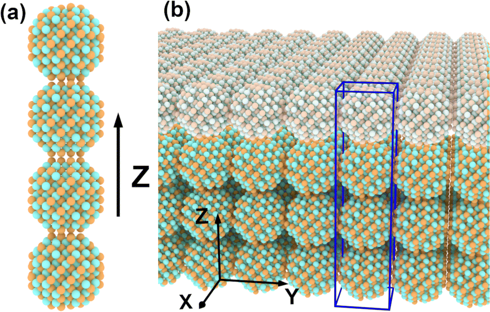 | ||
| Fig. 2 CQD distribution in the system. (a) A CQD molecule made of n = 4 quantum dots along the Z axis. (b) A CQD array made of n = 4 stacked layers (the upper of which is indicated in lighter colour), is obtained by repeating in 2D the CQD molecule (blue box). | ||
In the last step, the Schrödinger equation of n-CQD layers is formally identical to that of a two-dimensional array of CQD molecules (see Fig. 2(b))
 | (3) |
 are the quantum dot molecule positions in the 2D array,
  is the potential of the quantum dot molecule located at
  ,
,  is the array's wave function,
  its associated eigenenergy and
  is the wave vector in the array's reciprocal space. The basis to solve the latter is the set of CQD molecule eigenstates. The array wave functions are expanded as:44
 | (4) |
 is the wave function normalization constant, Nuc is the number of unit cells (QD molecules) in the array, bl are the expansion coefficients,
  is the array's reciprocal space vector and
  is the periodic function given by the Bloch's theorem.
This computational method yields the band structure of a system which is infinite along the in-plane directions, and is finite along the perpendicular direction (z axis). For comparison, we also calculated the electronic states in a 3D periodic array. As for the latter the CQD-molecule-based description cannot be used, we expanded its tight-binding wave function as a combination of individual CQD wave functions placed at each 3D lattice point:
 | (5) |
 are the positions of the 3D lattice points,
  are the m-th isolated CQD wave functions located at each lattice point and
  is the 3D array's reciprocal space vector. Equivalently to eqn (3), the potential
  is the 3D periodic repetition of the CQD potential.
The photon absorption coefficient of a CQD film has been calculated in previous works using the electric dipole moment approximation in Fermi's Golden Rule:15
 | (6) |
Before proceeding further, it is important to discuss the implications of the presence of the cell volume vuc in eqn (6): while in a 3D infinite array vuc is unambiguously defined by the interdot separation along each direction, in a 2D array vuc is not a well defined quantity. Indeed, in a 2D array the interdot separation adequately defines the unit cell area, auc, however, L⊥, the unit cell dimension along the perpendicular direction of the layer (the z direction in Fig. 2), is not well defined. This dimension also corresponds to the stack thickness. Theoretically, there is no inconsistency in considering L⊥ = nD in a n-layer stack, D being the CQD diameter, but larger values could also be used, if including any amount of vacuum above and below the layer limits, as in the case of an inter-layer separation larger than a bond length (the in-layer inter-dot separation). As the choice of vuc influences the values of α in eqn (6), it follows that α itself is not well defined. The Naperian absorbance
 | (7) |
 , where I0 and I are the incident and transmitted photon fluxes respectively, and
 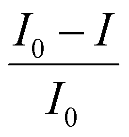 is the ratio between the light absorbed by the material and the incident light. Interestingly, this result is also applicable to unequally spaced CQD film stacks, and correctly accounts for the light absorbed by the total system (regardless of the inter-stack separation), which is simply the light absorbed by one layer times the number of layers in the stack. In contrast, the use of the absorption coefficient, eqn (6), would lead to different values for α for the same number of layers, depending on their separation (decreasing with increasing inter-layer distance), which is an unphysical result, as the empty space between layers cannot influence light absorption.
3 Results
Unlike in our previous work, where we focused on the properties of single 2D films,15 here we analyze monolayered and multilayered arrays of binary III–V CQDs (InX, X = P, As, Sb) to investigate the influence of the number of stacked layers, the interlayer separation and the material composition on their electronic structure and photon absorption coefficients. In these arrays the lowest energy conduction miniband, C1, is energetically well separated from the rest of the minibands and is, as pointed out above, a good candidate to act both as the IB in an IBSC, and as the ESC in an HCSC. In order to guarantee that it will contain both empty states, to accommodate electrons excited from the valence minibands, and filled states that can be promoted to higher conduction minibands, we, therefore, fixed the Fermi level position in the middle of C1 in the photon absorption calculations.3.1 Electronic structure
The analysis of the miniband structure requires the designation of a specific direction along the first Brillouin zone. With the aim of comparing the electronic structures of CQD arrays containing n stacks of identical 2D single layers, with n = 1, 2, …, the line joining the Γ and M point of the 2D reciprocal space has been selected (see inset in Fig. 3(e)), as this is the direction of maximum variation of the IB. This criterion has been established given that the comparison between the miniband structures of two- and three-dimensional arrays is not straightforward as the associated reciprocal spaces are not the same. | ||
| Fig. 3 Miniband structure for arrays constituted by (a, e and i) a single 2D layer, (b, f and j) 5 stacked layers, (c, g and k) 10 stacked layers, and (d, h and l) a 3D array of spherical InP (a–d), InAs (e–h), and InSb (i–l) CQDs with cation-rich surfaces. The energies on the vertical axis are relative to the vacuum level; the horizontal axis sweeps the Brillouin zone. The insets in (a)–(d) show a schematic view of the different structures considered. The inset in (e) identifies the path along the Brillouin zone together with the indexing of its major points. | ||
Fig. 3 shows our calculated electronic structures for n stacks of 2D arrays (with n = 1, 5, 10) of the 3 materials considered, separated by one bond length, together with a representation of the minibands widths for the corresponding fully 3D CQD array, for comparison. Schematic representations of the geometry of each system considered are presented as insets in Fig. 3. The array wave functions are expanded using different sets of single-dot eigenstates: for the purpose of this work we considered only eigenstates close to the CB [VB] edge, neglecting those laying ≈600 meV [≈200 meV] away, whose inclusion would broaden to the blue the calculated spectra, but would not alter the absorption onset in the regions of interest. In particular, we included 7, 8 and 11 eigenstates in the CB and 9, 7 and 6 eigenstates in the VB for InP, InAs and InSb, respectively. In the band structure of a single 2D layer, we find the existence of a narrow band separated from the rest, which is a good candidate for the role of both the ESC in HCSC and the IB in the IBSC. This is the band centered around −3.65 eV, −4.30 eV and −4 eV in InP (Fig. 3a), InAs (Fig. 3e), and InSb (Fig. 3i), respectively (where the energies are relative to the vacuum level).
Theoretical studies show that the IBSC efficiency reaches an optimum value for Eic = 0.7 eV and Evi = 1.23 eV,22 where Eic and Evi stand for the bandgap between the intermediate and conduction band, and between the valence and intermediate band, respectively. For comparison, in Fig. 4 we present the calculated Eic and Evi (empty symbols) as a function of the number of stacked layers for n = 1, …20, together with their values in the 3D case (solid lines). As n grows, the gaps’ widths of the stacked layers converge to those of the 3D structure. For n > 10 the difference between the two becomes negligible. We find a similar behaviour for the IB width in these structures (see Fig. 4c). We therefore conclude that, for practical purposes, a stack of 10 CQDs films has the features of a 3D array. Based on these results and the work by Krishna and Krich,46 we estimate maximum theoretical efficiencies of 24%, 44% and 52%, respectively, for IBSCs made of InP, InAs, and InSb CQD arrays.
 | ||
| Fig. 4 Minimum energy separation between (a) VB and IB (EVI), and (b) IB and CB (EIC), together with (c) IB width, as a function of the number of stacked layers of InP (blue triangles), InAs (green circles) and InSb (purple squares). The solid lines represent the energy separation [(a) and (b)] and IB width (c) of the corresponding 3D array. The dashed lines in (c) are the result of eqn (9). | ||
It is worth noting that the IB width in Fig. 4c ranges from tens to hundreds of meV. For HCSCs applications, band widths of the order of tens of meV not only approach the mono-energetic energy selective contact, but also improve band carrier transport compared to a single energy state, enhancing the solar cell efficiency. Based on this criterion, therefore, arrays of InP CQDs would be best suited as HCSCs contacts. Similarly, for applications in IBSCs, the presence of a narrow, but not completely flat, IB is of paramount importance, as it would allow transport of electrons from regions of high concentration (to which absorption from the VB would be suppressed), to regions of low concentration (from which absorption to the CB was suppressed) in the device, generating an electric current inside the IB.47–49 This crucial feature, is, however, not mentioned in any of the prevalent theoretical IBSC models, which assume instead the absence of any electric current in the IB (i.e., a nearly flat band). Since (i) the gaps between minibands in the multilayered 2D arrays are maintained as the number of stacked layers increases (Fig. 4), and (ii) their widths vary at most by 40 meV from a 2D single layer to a fully 3D structure in all materials considered, we conclude that, if these structures were exploited as the active region in an IBSC, the number of layers would not determine the ranges of energies in which light absorption is observed.
We mentioned earlier that the band used as IB/ESC originates from the coupling of the s-like CBM of individual CQDs along the structure. We derived a simple model (see ESI† for details) to (i) determine to what degree this conclusion is correct, (ii) estimate the IB width for 3D CQD arrays with arbitrary lattice constants along each direction, (iii) estimate the IB widths in stacked layers with arbitrary inter-layer separations, and, in short, (iv) simplify the modelling of this band in future device simulations and theoretical studies.
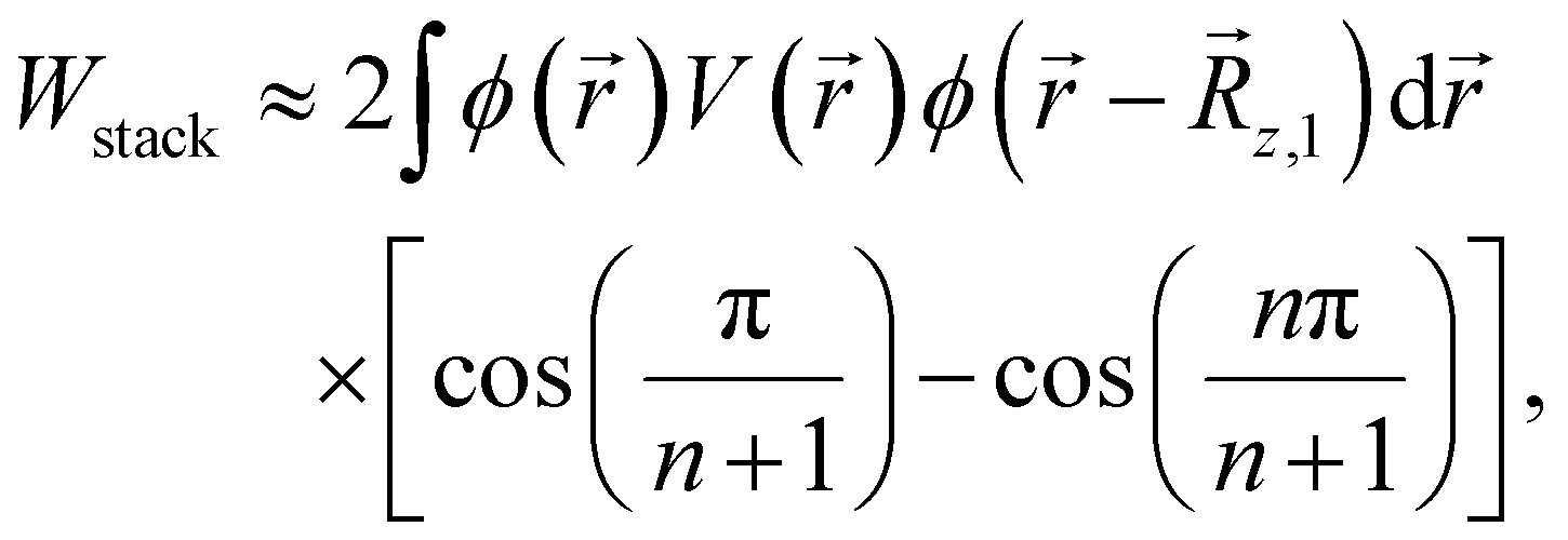
The results of this model are summarised in Fig. 5, which shows the contribution to the IB width, per array dimension, as a function of the interdot distance in each direction. By comparing it with Fig. 3, we see that the IB widths in panels (a, e and i) and (d, h and l), relative to a single 2D layer and a 3D array, respectively, approximately correspond to twice and three times the miniband width per dimension for the shortest interdot distance in Fig. 5. Similarly, the IB width for a 3D array [point (ii) above] can be obtained from Fig. 5 by summation of the miniband widths, considering the interdot distance along each direction. To obtain an estimate for the IB widths in n stacked layers with arbitrary inter-layer distances (iii), we need to consider an additional contribution to the width, due to the finiteness of the system along the stacking direction, which leads to a splitting of the minibands related to the sampling of the reciprocal lattice vectors (see ESI† for details):
 | (8) |
 | ||
| Fig. 5 Contribution to the IB width as a function of the interdot (center-to-center) distance in each direction. The lowest value stands for one cation–anion bond length separation between the CQD surfaces. InP (blue triangles), InAs (green circles) and InSb (purple squares). | ||
Using an asymptotic approximation for the difference of cosines, the IB width for a n-layer stack of CQDs with the same interdot distance along the in-plane and stack directions can be approximated by:
 | (9) |
As clearly shown in Fig. 5, the general trend of the IB width per dimension is an exponential decay with increasing dot-to-dot distance. By fitting the data in Fig. 5, we obtain WIB ∼ exp(−8.035d) for InP, WIB ∼ exp(−7.752d) for InAs and WIB ∼ exp(−11.26d) for InSb, where d (nm) is the interdot centre-to-centre distance. This result suggests the possibility of tailoring the IB width for specific applications by manipulating the interdot distance, hence the interdot coupling (which can be easily achieved through the use of suitably chosen capping groups).
3.2 Light absorption coefficient
The absorption coefficient in direct gap bulk materials is of the order of 106 m−1 for photon energies close to the bandgap.50 We expect similar values in CQD arrays, with the added benefits of an electronic structure fulfilling the IBSC criteria for optimal cell efficiency.When the wave function of an infinite (2D or 3D) array is expanded using a set of m eigenstates of an isolated CQD, m minibands are obtained, although the reciprocal space is different in 2D and 3D. When stacking n 2D films, the number of single-layer 2D minibands is multiplied by n in a two-dimensional reciprocal space. In general, in a system with μ minibands, light absorption involves μ(μ − 1)/2 interband transitions (i.e., all the vertical transitions from lower to higher minibands). In this work, computation of light absorption for a single 2D CQD layer involves 120, 105 and 136 transitions in InP, InAs and InSb, respectively. For n = 10 layers, the number of transitions that should be considered ranges from 11![[thin space (1/6-em)]](https://www.rsc.org/images/entities/char_2009.gif) 175 to 14365 in InAs and InSb, respectively. These considerations demonstrate that calculating light absorption in CQD arrays can quickly become computationally intensive, particularly for multilayered stacks. However, it is reasonable to expect that not all transitions will contribute equally to light absorption, and that the most significant contributions will come from a restricted subset, the remaining ones providing only negligible contributions, owing to selection rules, occupation numbers/probabilities/statistics and symmetry considerations. Taking advantage of this would allow the optimisation of the computational effort by reducing the number of transitions to be considered to the ‘effective’ ones. The crucial, and most difficult, part is their identification. We achieve this through two simple steps, and in what follows we will compare the results of this approach with those obtained with the full calculation and show that they are virtually the same.
175 to 14365 in InAs and InSb, respectively. These considerations demonstrate that calculating light absorption in CQD arrays can quickly become computationally intensive, particularly for multilayered stacks. However, it is reasonable to expect that not all transitions will contribute equally to light absorption, and that the most significant contributions will come from a restricted subset, the remaining ones providing only negligible contributions, owing to selection rules, occupation numbers/probabilities/statistics and symmetry considerations. Taking advantage of this would allow the optimisation of the computational effort by reducing the number of transitions to be considered to the ‘effective’ ones. The crucial, and most difficult, part is their identification. We achieve this through two simple steps, and in what follows we will compare the results of this approach with those obtained with the full calculation and show that they are virtually the same.
Considering the previous discussion on the electronic structure of infinite systems, indicating with mv and mc the number of valence and conduction minibands, respectively (and remembering that one additional band – the IB – needs also to be considered), light absorption in a 2D array would involve (mc + mv + 1)(mc + mv)/2 transitions. In the first step, assuming the Fermi level to be positioned in the middle of the IB, (as it is supposed to, for this structure to work effectively), it is possible to simplify the calculation by grouping the transitions into three distinct sets (that can also be associated with three well distinct energy ranges): (i) from the valence band to the intermediate band (VB → IB, mv transitions); (ii) from the intermediate band to the conduction band (IB → CB, mc transitions); and (iii) from the valence to the conduction band (VB → CB, mv × mc transitions). VB → VB and CB → CB transitions are neglected as the former are between occupied states and the latter between empty states. Therefore, the number of transitions reduces to mc + mv + mc × mv. Considering an equal number of valence and conduction minibands, this consideration tends to reduce asymptotically the number of transitions for a high number of minibands by up to ∼50%. Nevertheless, the computational requirements considerably increase for stacks: each original miniband in the infinite 2D array splits into n minibands when stacking n layers, as shown in Fig. 3. Potentially, the number of transitions increases roughly as n2, so that even the above simplifications are not helpful.
In the second step, we computed the absorbance of all transitions for the single 2D layer. Then, for each of the 3 sets mentioned above, we selected the transition with the highest absorption coefficient αmax and considered only transitions with α > 10% αmax neglecting all the rest, with the exception of those transitions involving a state degenerate with any whose α was above that threshold. After these transitions subsets had been determined, we used them (and the corresponding n minibands originating from the ones of the single layer), to compute the absorbance for the n-layer stacks. Therefore the full calculation needs to be carried out only for the single 2D layer, after which point the reduced set is used for the stack. Fig. 6–8 show the total Naperian absorbance at 300 K for a single 2D CQD layer, and for 5 and 10 stacked layers, separated by one bond length, for all structures considered, calculated using both the full (solid black line) and the ‘effective’ (colored areas) set of transitions. In every instance, only in-plane light polarization (i.e., along the x (100) and y (010) directions) has been considered. As we envision the implementation of these systems as active regions in IB solar cells with a tracking solar concentrator system, where light incidence would always be perpendicular to the 2D layer(s), polarization along the z axis was not considered.
 | ||
| Fig. 6 Naperian absorption coefficient calculated at 300 K for (a), (b) a single 2D array, (c), (d) five and (e), (f) ten stacked 2D arrays of InP dots with radius R = 11.9 Å and cation-rich surfaces. (a), (c) and (e): 100 polarization; (b), (d), and (f): 010 polarization. The results of the full calculation (solid lines) are compared with those of the reduced set (colored regions). | ||
 | ||
| Fig. 7 Same as Fig. 6 but for InAs dot arrays with R = 12.2 Å. | ||
 | ||
| Fig. 8 Same as Fig. 6 but for InSb dot arrays with R = 13.1 Å. | ||
As can be seen from these figures the simplification just discussed yields absorption profiles nearly identical to those obtained with the full calculation, but reduces the number of transitions by 87%, 85% and 57% in InP, InAs and InSb, respectively (the transitions included are indicated in the ESI†). This result is particularly important for solar cell device modelling applications, as it greatly reduces the computational cost, without reducing the accuracy.
The calculated Naperian absorbance of single-layer films are of the order of ∼10–2 in most cases. By using L⊥ = 2 nm (approximately the CQD diameter), we can estimate the order of magnitude of the absorption coefficient as α ∼ 5 × 10⁶ m−1, consistent with the light absorption coefficient of bulk materials.50 The Naperian absorbance also indicates that a single-layer CQD film can absorb ∼1 − exp(10–2) ∼ 1% of the incident light. The exception to this rule is InP, where we find the IB → CB absorption to be remarkably weak. This, combined with their strong dependence on light polarization, makes InP CQD arrays unsuitable for application as the active material in IBSCs.
The dramatic drop of absorbance we find in InP at low energies is consistent with that observed in the same energy range in single 2D layers of C atoms (graphene).51–54 Furthermore the value we predict for the absorbance of single layers of InSb and InAs CQDs in the range 0.5–0.8 eV is also quantitatively in agreement with that observed in graphene and other 2D systems, such as InAs nanomembranes.55 Our results therefore support the hypothesis of a universal behaviour of absorption in 2D materials,51–53 where the optical absorption in the region 0.5–1.2 eV is nearly independent of the photon energy and equal to a universal quantum of absorption AQ = πafs = 0.02293 (where afs ≈ 1/137 is the fine structure constant). However, our findings contradict the assumption that the absorbance of n layers is nAQ, a result derived from the Beer–Lambert law for weakly coupled layers. Our results indicate that the inter-layer coupling effect is relevant, and it degrades the absorption properties leading to A(n) < nA(1).
A natural question to ask at this point is whether, in terms of light absorption optimisation, a stack of 2D arrays is better than a single film. Or, in other words, if coupling between adjacent films enhances or reduces light absorption. To answer this question we present in Fig. 9 the maximum absorbances for each set of transitions in each material (and for each polarization) vs. the number of 2D layers, together with the calculated product of αmax for a single layer times the number of layers n. It is evident that the absorbance of a stack of n layers is less than n times the absorbance of a single layer, for transitions involving the IB (and most VB to CB transitions) in nearly all materials considered (with the exception of the VB to IB transitions in InSb). InAs stacks exhibit the largest differences, reaching reductions of the order of 50% for the (100) polarization. As an example, a 10-layer stack of InAs CQD films would absorb (1 − exp(−0.235)) ≈ 21% and (1 − exp(−0.653)) ≈ 48% of the photons with energy corresponding to the maximum absorption for the VB to CB transition, (and for light polarised along the 100 and 010 direction, respectively), whereas 10 uncoupled layers would absorb 1 − exp(−0.436) ≈ 35% and (1 − exp(−0.833) ≈ 57%) of the same photons, for the same light polarizations. We conclude that coupling between neighboring CQD films in a stack is detrimental to light absorption in IBSCs.
 | ||
| Fig. 9 Naperian absorbance maximum for transitions between miniband sets (VB, IB and CB), for each material and light polarization, as a function of the number of coupled 2D layers (symbols), and linear extrapolation of n times its value for a single-layer (see text, lines). (a) and (b): InP; (c) and (d): InAs; (e) and (f): InSb. | ||
A rough estimate regarding the separation at which stacked layers can be considered coupled can be obtained from Fig. 5, as the IB width is closely related to coupling: we see that when the interlayer distance increases by 0.5 nm (from its minimum value of 1 bond length), the contribution to the IB width can decrease by up to nearly 2 orders of magnitude (such that along that direction the coupling has a contribution to the IB width of the order of a few meV). At this point the system can be considered decoupled. Therefore the level of coupling achievable experimentally will depend on the type of passivation used (i.e., whether organic or inorganic) and on length of the eventual capping groups.
4 Conclusions
We carried out a theoretical atomistic study of the electronic structure and optical absorption of mono- and multi-layered two-dimensional arrays made of InP, InAs and InSb CQDs of realistic size, in view of their applications in HCSCs and IBSCs. Our results show that: (a) the band structure of a single 2D layer, exhibits a narrow band separated from the rest, which is a promising candidate for the role of both the ESC in HCSC and the IB in the IBSC; (b) this band is created exclusively by the coupling of the CBM state of the quantum dots throughout the material – as a consequence, since the equation for a band created by the coupling of single states is analytic, the modelling of the IB emerging in CQD arrays should be easily implementable in a device simulator; (c) the IB width can be tailored for specific applications by manipulating the interdot distance, through the use of suitably chosen capping groups; (d) as the number of stacked layers n increases, the value of the IB width converges to that of the 3D array (and, for practical purposes, a stack of 10 CQDs films has the features of a 3D array), and we derived a simple model to calculate it for any value of n; (e) the gaps of the multilayered 2D arrays are maintained as n increases, i.e., if these structures were exploited as the active region in an IBSC, the number of layers would not determine the ranges of energies in which light absorption is observed; (f) based on the latter energies, we estimate maximum theoretical efficiencies of 24%, 44% and 52%, respectively, for IBSCs made of InP, InAs, and InSb CQD arrays; (g) only a subset of the total number of electronic transitions between all different CQD levels are relevant to reproduce the light absorption coefficient of an array; (h) InP CQD arrays are unsuitable for IBSCs applications since the transitions to and from the IB are very weak (however, we found them to be well suited as ESC in HCSCs owing to their narrow IB); (i) stacking uncoupled CQD layers does not increase light absorption compared to the same number of individual 2D arrays, as absorption is proportional to the number of layers composing the stack, i.e., A(n) = nA(1); (l) coupling between neighboring CQD films in a stack, however, is detrimental to light absorption in IBSCs, yielding A(n) < nA(1).Data availability
The data supporting this article have been included as part of the ESI.†Conflicts of interest
The authors declare no conflicts of interest.Acknowledgements
R. V. H. H. gratefully acknowledges financial support from the Spanish Junta de Andalucía through a Doctoral Training Grant. M. C. thanks the School of Electronic & Electrical Engineering, University of Leeds, for financial support. F. M. G. C. gratefully acknowledges grant C-ING-208-UGR23 funded by Consejería de Universidad, Investigación e Innovación and by ERDF Andalusia Program 2021-2027.References
- I. Ramiro, B. Kundu, M. Dalmases, O. Özdemir, M. Pedrosa and G. Konstantatos, ACS Nano, 2020, 14, 7161–7169 CrossRef CAS PubMed
.
- M.-J. Choi, S. Kim, H. Lim, J. Choi, D. M. Sim, S. Yim, B. T. Ahn, J. Y. Kim and Y. S. Jung, Adv. Mater., 2016, 28, 1780–1787 CrossRef CAS PubMed
- M.-J. Choi, J. Oh, J.-K. Yoo, J. Choi, D. M. Sim and Y. S. Jung, Energy Environ. Sci., 2014, 7, 3052–3060 RSC
- I. V. Martynenko, A. P. Litvin, F. Purcell-Milton, A. V. Baranov, A. V. Fedorov and Y. K. Gun'ko, J. Mater. Chem. B, 2017, 5, 6701–6727 RSC
- Y. Zhao, J. Chen, Z. Hu, Y. Chen, Y. Tao, L. Wang, L. Li, P. Wang, H.-Y. Li, J. Zhang, J. Tang and H. Liu, Biosens. Bioelectron., 2022, 202, 113974 CrossRef CAS PubMed
- C. Livache, B. Martinez, N. Goubet, C. Gréboval, J. Qu, A. Chu, S. Royer, S. Ithurria, M. G. Silly, B. Dubertret and E. Lhuillier, Nat. Commun., 2019, 10, 2125 CrossRef PubMed
- T. Nakotte, H. Luo and J. Pietryga, Nanomaterials, 2020, 10, 172 Search PubMed
- R. Sliz, M. Lejay, J. Z. Fan, M.-J. Choi, S. Kinge, S. Hoogland, T. Fabritius, F. P. García de Arquer and E. H. Sargent, ACS Nano, 2019, 13, 11988–11995 Search PubMed
- Q. Song, Y. Xu, Z. Zhou, H. Liang, M. Zhang, G. Zhu, J. Yang and P. Yan, ACS Photonics, 2022, 9, 2520–2527 CrossRef CAS
- J. Yang, M. K. Choi, U. J. Yang, S. Y. Kim, Y. S. Kim, J. H. Kim, D.-H. Kim and T. Hyeon, Nano Lett., 2021, 21, 26–33 CrossRef CAS PubMed
- L. Liu, R. D. Septianto, S. Z. Bisri, Y. Ishida, T. Aida and Y. Iwasa, Nanoscale, 2021, 13, 14001–14007 RSC
- J.-H. Choi, A. T. Fafarman, S. J. Oh, D.-K. Ko, D. K. Kim, B. T. Diroll, S. Muramoto, J. G. Gillen, C. B. Murray and C. R. Kagan, Nano Lett., 2012, 12, 2631–2638 CrossRef CAS PubMed
- E. L. Rosen, A. M. Sawvel, D. J. Milliron and B. A. Helms, Chem. Mater., 2014, 26, 2214–2217 CrossRef CAS
- R. V. H. Hahn, S. Rodríguez-Bolívar, P. Rodosthenous, E. S. Skibinsky-Gitlin, M. Califano and F. M. Gómez-Campos, Nanomaterials, 2022, 12, 3387 CrossRef CAS PubMed
- E. S. Skibinsky-Gitlin, S. Rodríguez-Bolívar, M. Califano and F. M. Gómez-Campos, Nanoscale Adv., 2020, 2, 384–393 RSC
- J. Pinna, E. Pili, R. Mehrabi Koushki, D. S. Gavhane, F. Carlà, B. J. Kooi, G. Portale and M. A. Loi, ACS Nano, 2024, 18, 1936–0851 CrossRef PubMed
- F. A. N. Mawaddah and S. Z. Bisri, Nanomaterials, 2024, 14, 1328 CrossRef CAS PubMed
- F. M. Gómez-Campos, S. Rodríguez-Bolívar, E. S. Skibinsky-Gitlin and M. Califano, Nanoscale, 2018, 10, 9679–9690 Search PubMed
- E. S. Skibinsky-Gitlin, S. Rodríguez-Bolívar, M. Califano and F. M. Gómez-Campos, Phys. Chem. Chem. Phys., 2019, 21, 25872–25879 RSC
- J.-S. Lee, M. V. Kovalenko, J. Huang, D. S. Chung and D. V. Talapin, Nat. Nanotechnol., 2011, 6, 348–352 CrossRef CAS PubMed
- R. T. Ross and A. J. Nozik, J. Appl. Phys., 1982, 53, 3813–3818 CrossRef CAS
- A. Luque and A. Martí, Phys. Rev. Lett., 1997, 78, 5014–5017 CrossRef CAS
- A. Martí, E. Antolín and I. Ramiro, Phys. Rev. Appl., 2022, 18, 064048 CrossRef
- I. Ramiro and A. Martí, Prog. Photovolt.: Res. Appl., 2021, 29, 705–713 CrossRef CAS
- V. Popescu, G. Bester, M. C. Hanna, A. G. Norman and A. Zunger, Phys. Rev. B:Condens. Matter Mater. Phys., 2008, 78, 205321 CrossRef
- S. A. Blokhin, A. V. Sakharov, A. M. Nadtochy, A. S. Pauysov, M. V. Maximov, N. N. Ledentsov, A. R. Kovsh, S. S. Mikhrin, V. M. Lantratov, S. A. Mintairov, N. A. Kaluzhniy and M. Z. Shvarts, Semiconductors, 2009, 43, 514–518 Search PubMed
- S. Tamang, C. Lincheneau, Y. Hermans, S. Jeong and P. Reiss, Chem. Mater., 2016, 28, 2491–2506 CrossRef CAS
- T. Kim, D. Shin, M. Kim, H. Kim, E. Cho, M. Choi, J. Kim, E. Jang and S. Jeong, ACS Energy Lett., 2023, 8, 447–456 Search PubMed
- A. A. Guzelian, J. E. B. Katari, A. V. Kadavanich, U. Banin, K. Hamad, E. Juban, A. P. Alivisatos, R. H. Wolters, C. C. Arnold and J. R. Heath, J. Phys. Chem., 1996, 100, 7212–7219 CrossRef CAS
- A. A. Guzelian, U. Banin, A. V. Kadavanich, X. Peng and A. P. Alivisatos, Appl. Phys. Lett., 1996, 69, 1432–1434 Search PubMed
- S. Busatto, M. de Ruiter, J. T. B. H. Jastrzebski, W. Albrecht, V. Pinchetti, S. Brovelli, S. Bals, M.-E. Moret and C. de Mello Donega, ACS Nano, 2020, 14, 13146–13160 CrossRef CAS PubMed
- J. Jasieniak and P. Mulvaney, J. Am. Chem. Soc., 2007, 129, 2841–2848 CrossRef CAS PubMed
- D. M. Balazs, B. M. Matysiak, J. Momand, A. G. Shulga, M. Ibáñez, M. V. Kovalenko, B. J. Kooi and M. A. Loi, Adv. Mater., 2018, 30, 1802265 Search PubMed
- D. M. Balazs, D. N. Dirin, H.-H. Fang, L. Protesescu, G. H. ten Brink, B. J. Kooi, M. V. Kovalenko and M. A. Loi, ACS Nano, 2015, 9, 11951–11959 CrossRef CAS PubMed
- C. van Overbeek, J. L. Peters, S. A. P. van Rossum, M. Smits, M. A. van Huis and D. Vanmaekelbergh, J. Phys. Chem. C, 2018, 122, 12464–12473 CrossRef CAS PubMed
- J. J. Geuchies, C. van Overbeek, W. H. Evers, B. Goris, A. de Backer, A. P. Gantapara, F. T. Rabouw, J. Hilhorst, J. L. Peters, O. Konovalov, A. V. Petukhov, M. Dijkstra, L. D. A. Siebbeles, S. van Aert, S. Bals and D. Vanmaekelbergh, Nat. Mater., 2016, 15, 1248–1254 CrossRef CAS PubMed
- S. R. Mirnaziry, M. A. Shameli and L. Yousefi, Sci. Rep., 2022, 12, 13259 CrossRef CAS PubMed
- J. Pinna, R. Mehrabi Koushki, D. S. Gavhane, M. Ahmadi, S. Mutalik, M. Zohaib, L. Protesescu, B. J. Kooi, G. Portale and M. A. Loi, Adv. Mater., 2023, 35, 2207364 Search PubMed
- A. Abelson, C. Qian, T. Salk, Z. Luan, K. Fu, J.-G. Zheng, J. L. Wardini and M. Law, Nat. Mater., 2020, 19, 49–55 CAS
- J. C. daSilva, M. A. Smeaton, T. A. Dunbar, Y. Xu, D. M. Balazs, L. F. Kourkoutis and T. Hanrath, Nano Lett., 2020, 20, 5267–5274 CAS
- G. Bester, J. Phys.: Condens. Matter, 2008, 21, 023202 Search PubMed
- L.-W. Wang and A. Zunger, Phys. Rev. B:Condens. Matter Mater. Phys., 1995, 51, 17398–17416 Search PubMed
- A. Canning, L. Wang, A. Williamson and A. Zunger, J. Comput. Phys., 2000, 160, 29–41 Search PubMed
- F. M. Gómez-Campos, S. Rodríguez-Bolívar and M. Califano, J. Nanomater., 2019, 2019, 5106909 Search PubMed
- T. G. Mayerhofer, S. Pahlow and J. Popp, ChemPhysChem, 2020, 21, 2029–2046 CrossRef PubMed
- A. Krishna and J. J. Krich, J. Opt., 2016, 18, 074010 Search PubMed
- A. Stolow, D. J. Gayowsky, M. M. Wilkins and J. J. Krich, 2020 47th IEEE Photovoltaic Specialists Conference (PVSC), 2020, pp. 1645–1650.
- E. C. Dumitrescu, M. M. Wilkins and J. J. Krich, J. Comput. Electron., 2020, 19, 111–127 Search PubMed
- R. Strandberg and T. W. Reenaas, Prog. Photovolt.: Res. Appl., 2011, 19, 21–32 CAS
- H. J. Lee, M. M. A. Gamel, P. J. Ker, M. Z. Jamaludin, Y. H. Wong and J. P. R. David, J. Electron. Mater., 2022, 51, 6082–6107 Search PubMed
- K. F. Mak, M. Y. Sfeir, Y. Wu, C. H. Lui, J. A. Misewich and T. F. Heinz, Phys. Rev. Lett., 2008, 101, 196405 CrossRef PubMed
- R. R. Nair, P. Blake, A. N. Grigorenko, K. S. Novoselov, T. J. Booth, T. Stauber, N. M. R. Peres and A. K. Geim, Science, 2008, 320, 1308 Search PubMed
- K. F. Mak, L. Ju, F. Wang and T. F. Heinz, Solid State Commun., 2012, 152, 1341–1349 Search PubMed
- D. J. Merthe and V. V. Kresin, Phys. Rev. B, 2016, 94, 205439 CrossRef
- H. Fang, H. A. Bechtel, E. Plis, M. C. Martin, S. Krishna and E. Y. A. Javey, Proc. Natl. Acad. Sci. U. S. A., 2013, 110, 11688 CrossRef CAS PubMed
Footnote |
| † Electronic supplementary information (ESI) available. See DOI: https://doi.org/10.1039/d4nr04841e |
| This journal is © The Royal Society of Chemistry 2025 |