
 Open Access Article
 This Open Access Article is licensed under a Creative Commons Attribution-Non Commercial 3.0 Unported Licence
Improving the long-term stability of new-generation perovskite-based TCOs using binary and ternary oxides capping layers†
Moussa
Mezhoud
 *a,
Martando
Rath
a,
Stéphanie
Gascoin
a,
Sylvain
Duprey
b,
Philippe
Marie
b,
Julien
Cardin
b,
Christophe
Labbé
b,
Wilfrid
Prellier
a and
Ulrike
Lüders
*a
*a,
Martando
Rath
a,
Stéphanie
Gascoin
a,
Sylvain
Duprey
b,
Philippe
Marie
b,
Julien
Cardin
b,
Christophe
Labbé
b,
Wilfrid
Prellier
a and
Ulrike
Lüders
*a
aUniversité de Caen Normandie, ENSICAEN, CNRS UMR 6508, CRISMAT, Normandie Univ., 14000 Caen, France. E-mail: moussa.mezhoud@ensicaen.fr; ulrike.luders@ensicaen.fr
bCIMAP, ENSICAEN, UNICAEN, CNRS UMR6252, CEA, Normandie Univ, 6 Bd Maréchal Juin, 14050 Caen, cedex 4, France
First published on 4th June 2025
Abstract
We report the impact of capping layers on vanadate based transparent conductive oxides (TCOs) to prolong the thermal stability with a minimal loss of electrical conductivity during heat treatment in ambient environment. In the present study, various capping layers (amorphous Al2O3, LaAlO3 (LAO), TiO2 grown at base pressure and TiO2 deposited under oxygen partial pressure) are grown in situ on polycrystalline perovskite SrVO3 (SVO) thin films using Pulsed Laser Deposition (PLD). The results show that amorphous LaAlO3 is the most promising capping layer among the oxide layers, to preserve both electrical and optical properties of perovskite SVO films from natural as well as artificial aging. Our present approach for a capping layer on SVO may address the long-term stability issues of correlated TCOs and would open an opportunity for the future oxide electronics applications.
Introduction
The progress in creating next-generation optoelectronic devices such as flat-panel displays, smartphones, sensors, and solar cells is intricately tied to the development of a vital component in these devices: transparent and conducting oxides (TCOs).1–7 These materials possess a unique combination of electrical conductivity and optical transparency, two competing properties that are notoriously challenging to achieve within a single material. Recently, a new family of transparent and conducting materials has been discovered in the oxides perovskite of structure ABO3,8–13 arousing great interest in the scientific community.SrVO3 (SVO) emerges as a highly promising material,11,14–20 offering a compelling alternative to commonly used transparent conducting oxides such as Indium Tin Oxide (ITO),21 due to its remarkable optical and electrical properties, along with the abundant and low-cost nature of its chemical elements constituent. However, numerous studies have pointed to the critical issue of SVO instability when exposed to oxygen-containing atmospheres.22–26 The degradation, primarily attributed to the presence of V4+, an unstable oxidation state,27 has been observed to lead to the formation of insulating over-oxidized phases V5+ phases, such as Sr2V2O7 or Sr-rich Sr3V2O8 on the surface of the SVO film.28 Due to their electrically insulating nature, these phases drastically alter the surface conductivity and are known to be soluble in water,26,27,29,30 which provides a significant barrier to the long-term use of SVO as a TCOs. Moreover, the surface instability of perovskite oxides is a well known issue when exposed to different environmental conditions, such as variations in temperature, humidity, and gas atmospheres, more specifically, which contains oxygen.26–28,31,32 This phenomenon gives rise to surface reconstruction and segregation, formation of surface defects, and phase transformations, all of which can drastically alter the material's properties.33–36 Consequently, surface instability has emerged as a pivotal factor that impacts the functionality, stability, and durability of perovskite oxide-based devices and technologies. These drawbacks of the vanadate TCOs may provide an important obstacle to widespread industrial acceptance of this extremely promising new TCOs.
In order to address this issue, the concept of using capping layers to engineer and enhance the properties of perovskite oxides has gained significant attention in recent years.37–41 Capping layers, which are very thin films deposited on the surface of perovskite oxide materials, offer a powerful approach to tailor the structural, electrical, and chemical characteristics of these functional materials. For example, an enhancement in the Curie temperature of SrRuO3 thin films has been reported using a capping layer of SrTiO3 (STO) that reduces the oxygen octahedral rotation.42 STO has also been utilized to stabilize the Sr3Al2O6 sacrificial layer in ambient atmosphere and for growth of functional oxides at high temperatures.43,44
For vanadates-based perovskite oxides, capping layers has been used to stabilize the unstable V3+ and V4+ oxidation states. Kumar et al.45 employed a thin film of 8 nm LAO as the capping layer of PrVO3 (PVO) films to prevent oxydation of V3+ to V4+, which has considerably reduced the magentic dead layer in PVO films. Recently, Caspi et al.46 and Cohen et al.47 investigated the effectiveness of various amorphous capping layer, including TiO2−δ, Al2O3−δ, ZrO2−δ, and SiO2−δ as well as epitaxial SrTiO3−δ, in preventing the oxidation of V4+ to V5+ in epitaxial SVO films. Their results showed that all tested capping layers successfully preserved the V4+ state at room temperature, in contrast to the oxidation observed in the uncapped film. However, their study was limited to ambient conditions and did not address long-term stability, which is the primary objective of this work. Since oxygen diffusion is strongly temperature dependent, room temperature measurements alone cannot distinguish between materials with different intrinsic oxygen diffusion properties. In contrast, in an earlier study, we have investigated the accelerated aging process of SVO films at different temperatures (150 °C to 250 °C) and observed that when exposed to 250 °C, SVO films without capping layers lose their crystalline structure and become insulating,27 so in the present study we investigate the effect of using different capping layers reported in literature such as TiO2, LAO, and Al2O3 on the stability of SVO films at 250 °C, the temperature at which unprotected films completely degrade. The intention of exposing the material to non-ambient conditions, including elevated temperature, is to accelerate the aging process and provide a prediction of the material's stability with different capping layers over an extended period, thereby identifying the most effective capping layer. If a capping layer can prevent the degradation of SVO films at 250 °C, it strongly indicates that the same layer would effectively ensure long-term stability under ambient conditions. This is particularly relevant for solar cells, which can be exposed to relatively high temperatures in certain geographic regions. Hence also the choice to concentrate this study on polycrystalline films, which are closer to the potential application in real devices than epitaxial thin films. Thus, the thickness of the capping layers was maintained within the range of 7–10 nm. Since the critical thickness for protection is material-dependent, relatively thick capping layers were selected in this study to ensure that all films exceed the critical thickness threshold, which typically on the order of a few unit cells.31,44 This approach allows for clearer comparison of the intrinsic protective efficiency of different materials. Furthermore, in our previous works,26,27 we carefully analyzed the vanadium oxidation state as a function of aging. For unprotected SVO films aged at 200 °C, we observed the formation of a top oxidized layer, composed of amorphous Sr-rich phases such as Sr3V2O8, as revealed by TEM images. X-ray absorption spectroscopy (XAS) confirmed that vanadium in this layer was in the V5+ oxidation state. When the aging temperature was increased to 250 °C, the V5+ phase extended throughout the entire film thickness, indicating that oxidation progresses from the surface inward due to the penetration of oxygen absorbed at the film surface and its diffusion toward the film/substrate interface. For the capped films in this study, we are not able to directly analyze the vanadium oxidation state. XAS and XPS have a sampling depth limited to only a few nanometers. Therefore, it is impossible to study the vanadium oxidation state through the thick capping layers used in this study. However, based on our previous work, we have observed that the transition from V4+ to V5+ is accompanied by structural, optical, and electrical changes, which are not present in the protected SVO films. Therefore, in this work, we focused only on these functional properties as indirect indicators of oxidation and, consequently, degradation.
Regarding the efficiency of the oxidized top layer as a capping layer, our previous study27 showed that while it initially acts as a passivating layer at room temperature, its water solubility makes it vulnerable to degradation upon exposure to moisture. In addition, at higher aging temperature, the passivation is not efficient anymore, and the full film is destroyed, emphasizing the need for a more stable capping layer under these conditions.
Methods
Samples preparation
Polycrystalline targets of Sr2V2O7, TiO2, Al2O3 and LaAlO3 were prepared by standard solid-state reaction route. A series of polycrystalline SVO films is grown with different capping layers such as amorphous Al2O3 (a-Al2O3), LaAlO3 (a-LAO), TiO2 under vacuum (a-TiO2-V) and TiO2 under oxygen partial pressure (a-TiO2-O). Eagle XG slim glass substrates with 7 nm thick TiO2 layer as a buffer layer was used to grow in situ polycrystalline SVO films. The deposition was carried out in a Pulsed Laser Deposition (PLD) setup using an ultraviolet KrF excimer laser with a wavelength of 248 nm. All SVO films, TiO2 buffer layers and different capping layers are deposited with a laser energy of 200 mJ corresponding to a fluence of around 1.6–2.0 J cm−2 and with a laser repetition rate of 5 Hz as discussed in our previous reports.27 An optimized growth temperature of 600 °C was used for the TiO2 buffer layer and the SVO films while the capping layers were deposited at 100 °C to obtain amorphous layers. The TiO2 buffer layers were deposited under an oxygen pressure of 1 × 10⁻² mbar, while the SVO films were deposited under vacuum, with a pressure of around 2.0 × 10⁻⁶ mbar, when the sample is at deposition temperature. The capping layers were deposited under the same atmosphere, except the a-TiO2-O capping layer, where an oxygen O2 partial pressure (P(O2) = 1 × 10⁻² mbar) was used. The thicknesses of the buffer and capping layers were approximately 7–10 nm and 25–30 nm for SVO films, as determined by X-Ray Reflectivity (XRR) measurements.The Sr![[thin space (1/6-em)]](https://www.rsc.org/images/entities/char_2009.gif) :V stoichiometry of the as-grown samples is approximately 1.2 ± 0.3, which corresponds to stoichiometric SrVO3 films. This analysis was previously performed using XPS in a separate study.26 An earlier Rutherford Backscattering study has also shown a bulk cation stoichiometry of the SVO films.14 Regarding the stoichiometry of the capping layers, we conducted XAS measurements solely on the a-TiO2-V sample. These measurements, shown in Fig. S1 of the ESI,† demonstrate that the TiO2 layer exhibits a Ti4+ signature after aging, and the obtained XAS spectrum displaying the characteristic shape of Ti4+. Moreover, for the growth of stoichiometric a-Al2O3 thin films, we used the same optimized conditions reported by Upadhyay in their PhD thesis,48 which were also applied for the growth of a-LAO capping layers.
:V stoichiometry of the as-grown samples is approximately 1.2 ± 0.3, which corresponds to stoichiometric SrVO3 films. This analysis was previously performed using XPS in a separate study.26 An earlier Rutherford Backscattering study has also shown a bulk cation stoichiometry of the SVO films.14 Regarding the stoichiometry of the capping layers, we conducted XAS measurements solely on the a-TiO2-V sample. These measurements, shown in Fig. S1 of the ESI,† demonstrate that the TiO2 layer exhibits a Ti4+ signature after aging, and the obtained XAS spectrum displaying the characteristic shape of Ti4+. Moreover, for the growth of stoichiometric a-Al2O3 thin films, we used the same optimized conditions reported by Upadhyay in their PhD thesis,48 which were also applied for the growth of a-LAO capping layers.
Structural characterization
The crystal structure of polycrystalline films with and without capping layers, before and after heat treatment, was studied by Grazing Incidence X-Ray Diffraction (GIXRD) using a PANalytical X'Pert Materials Research Diffractometer (MRD) with monochromatic Cu Kα1 radiation and wavelength of 1.5406 Å. X-ray reflectivity (XRR) using the same instrument was used to determine thicknesses of the samples. The exact values of the film thicknesses were determined by considering the positions of the maxima of the XRR oscillations, and a fit of the sinus of these positions vs. the square of the order number. The slope of the fit is used to calculate the film thickness.Electrical characterization
The thermal annealing of as grown samples with and without capping layers was carried out on a hot plate under ambient atmosphere, for 24 h. The samples were placed on the hot plate at room temperature, and the four-point probe configuration for the resistivity measurement was positioned on the surface of the samples. Then, to study the aging effect of these samples, the temperature of the hot plate was increased at a heating rate of 65 °C min−1 until it reached 250 °C. By applying a current, the electrical resistance with time was recorded using a Keithley 2450 sourcemeter, once the desired temperature was reached. The initial resistance value at t = 0 min corresponds to the room temperature resistance of the sample before the beginning of the heat treatment. Finally, the electrical resistivity of the aged samples with time was calculated from the resistance values, by considering the geometrical configuration of the sample and the measurement setup. Due to the continuous evolution of film thickness during aging, the as-grown thickness of each sample was used as an approximation for resistivity calculations.Optical characterizations
The optical transmission of the samples was measured using conventional transmission mode of a Lambda 1050 PerkinElmer spectrophotometer in the UV-Visible-Near Infrared (UV-Vis-NIR) range. Variable-angle spectroscopic ellipsometry (VASE) was carried out at three different incident angles 60°, 70° and 75°, in reflection mode from the photon energies from 0.6 to 6.5 eV (UV-Vis-NIR) using a HORIBA Jobin Yvon instrument. The optimized incident angle 70° from the sample normal was used to calculate the ellipsometry parameters (Δ, Ψ) and followed by the other optical parameters such as the optical coefficient (n + ik) and complex dielectric constant, ε(ω) = ε1(ω) + iε2(ω) were extracted of the samples using the DeltaPsi2 software. The collected SE data in the near IR to UV range was fitted with the configuration of air/capping layer/SVO film/substrate, where the Eagle glass substrate with buffered TiO2 layer was separately fitted. It is important to note that the thicknesses of each layer such as TiO2 buffer layer, SVO film and all capping layers were determined using XRR measurements and their values were inserted in the model during the fitting. New amorphous oscillator functions were used to model the insulating capping layers and TiO2 buffer layer on the glass substrate. Besides, a Drude oscillator and an extra Lorentz oscillator with new amorphous oscillators were used for the metallic SVO thin film. A constant value ε∞ is added to the real part ε1(ω) to fit the model further at even higher energy.Results and discussion
Fig. 1a depicts the GIXRD patterns of SVO thin films grown on TiO2 buffered glass substrate without capping layer and with four different capping layers named a-LAO, a-Al2O3, a-TiO2-V and a-TiO2-O, after annealing at 250 °C for 24 h. For the SVO film without capping layer (orange line), all the diffraction peaks related to the SVO phase (Pm![[3 with combining macron]](https://www.rsc.org/images/entities/char_0033_0304.gif) m) have vanished and the sample exhibits an amorphous nature as observed previously.27 For the films with capping layers, the presence of diffraction peaks of different crystallographic planes such as (110), (111), (200), (211), (220) and (310) of the SVO phase confirms the polycrystalline nature of the films, even after an annealing at 250 °C for 24 h. Furthermore, we have not found any peaks related to secondary phases in the XRD patterns, confirming the stability of the SVO phase after 24 h of heat treatment in the limits of the technique. Among all capping layers, SVO films with a-LAO, a-Al2O3 and a-TiO2-O show clear and distinguished peaks even at higher 2θ angles. However, the sample with a-TiO2-V capping layer shows slightly smaller intensities compared with the other samples, suggesting a lower protection effect of the a-TiO2-V capping layers. Regarding the evolution of the lattice parameter of the SVO films with the capping layers, we observed an increase in all samples except for that capped with a-LAO. For example, based on the most intense (110) reflection, the lattice parameter increased from 3.845 Å in the bare SVO film before aging to 3.864 Å in the film capped with a-TiO2-V after aging. However, for the film capped with a-LAO, a decrease to 3.831 Å was observed. The resulting lattice parameter of the crystalline film is not only a result of the chemical composition of the film, but also of eventual residual stress in the sample.
m) have vanished and the sample exhibits an amorphous nature as observed previously.27 For the films with capping layers, the presence of diffraction peaks of different crystallographic planes such as (110), (111), (200), (211), (220) and (310) of the SVO phase confirms the polycrystalline nature of the films, even after an annealing at 250 °C for 24 h. Furthermore, we have not found any peaks related to secondary phases in the XRD patterns, confirming the stability of the SVO phase after 24 h of heat treatment in the limits of the technique. Among all capping layers, SVO films with a-LAO, a-Al2O3 and a-TiO2-O show clear and distinguished peaks even at higher 2θ angles. However, the sample with a-TiO2-V capping layer shows slightly smaller intensities compared with the other samples, suggesting a lower protection effect of the a-TiO2-V capping layers. Regarding the evolution of the lattice parameter of the SVO films with the capping layers, we observed an increase in all samples except for that capped with a-LAO. For example, based on the most intense (110) reflection, the lattice parameter increased from 3.845 Å in the bare SVO film before aging to 3.864 Å in the film capped with a-TiO2-V after aging. However, for the film capped with a-LAO, a decrease to 3.831 Å was observed. The resulting lattice parameter of the crystalline film is not only a result of the chemical composition of the film, but also of eventual residual stress in the sample.
 | ||
| Fig. 1 (a) GIXRD patterns of SVO thin films grown on TiO2 buffered glass substrate without and with different capping layers, after heat treatment at 250 °C for 24 h in air. (b) Effect of annealing temperature on the thickness of the samples before and after heat treatment. | ||
Fig. 1b show the role of annealing temperature on the evolution of the thickness of the SVO samples before and after aging.27 The non-capped SVO film annealed at 250 °C (orange color) shows a significant thickness increase (from 35 nm to 48 nm, i.e. 27%), which is not observed for the capped films. The thickness of SVO with a-LAO and a-Al2O3 capping layers show a minimal increase i.e. around 3 and 5%, respectively, under heat treatment at 250 °C for 24 h in air. However, the thickness of the sample with a-TiO2 layers deposited under oxygen atmosphere or in vacuum, shows a stronger thickness increase (i.e. 11 and 17%, respectively, compared to the as grown film). The observed thickness increase is consistent with our previous work,27 where we studied the aging of unprotected SVO films at different temperatures (150, 200, and 250 °C). The results revealed that thickness expansion was proportional to the aging temperature, with films aged at 250 °C exhibiting a greater increase than those aged at 150 °C. This was attributed to oxygen incorporation, a hypothesis further supported in the present study. Specifically, significant thickness increases were observed only in films with less effective capping layers, such as TiO2 or uncapped SVO, while Al-based capping layers, which act as oxygen diffusion barriers, showed only a very limited expansion (∼4%). This increase in thickness suggests that additional oxygen atoms are being incorporated into the film, but it is well known that the dense perovskite structure sustains only difficultly those supplementary atoms. Instead, this incorporation leads to the formation of amorphous phases, such as Sr2V2O7 and Sr3V2O8, which accommodate 3.5 or 4 oxygen atoms per vanadium, respectively, compared to just 3 oxygen atoms in the original ABO3 perovskite structure. However, their crystalline structure is profoundly different from the perovskite structure, which is probably the reason of the amorphous nature of the over-oxidized phases observed by Rath et al.27 A hypothesis, which has also been supported by a decrease of the density of SVO films when the proportion of these amorphous phases increases.27
The GIXRD and XRR measurements show that after heat treatment at 250 °C, SVO films with a-LAO and a-Al2O3 capping layers preserve their crystalline structure without further increase of thickness. However, for SVO films protected with a-TiO2 capping layers, the intensity of diffraction peaks diminishes with increasing the total thickness of the films. These two observations point to a weaker protective character of the TiO2 layers, leading to a partial degradation of SVO films.
Fig. 2 shows the evolution of electrical resistivity of the polycrystalline SVO films with and without capping layers during the heat treatment. As expected, the SVO film without capping layer shows an increasing resistivity.27 After 24 h, the sample turns into a bad conductor with the destruction of its perovskite structure, which is confirmed from GIXRD results. For SVO films with different capping layers, the SVO films with a-LAO and a-Al2O3 capping layers show during the heat treatments a small increase of the resistivity, quantified here by the ratio between the resistivity after 24 h of aging (ρ24h) and the initial resistivity value before aging (ρ0) of 1.33 and 1.53, respectively. Interestingly, the majority of conductivity loss occurs in the early stages of aging, as shown in Fig. S2.† Specifically, 79% of the conductivity loss for a-LAO and 87% for a-Al2O3 happens within the first 10 minutes of aging. It is worth to note that our operando resistivity measurements are conducted at 10 min intervals, making it impossible to precisely determine whether the observed resistivity increase occurs within the first minute or gradually over the full 10 minutes period. However, in our previous work,26 we performed operando XAS measurements during aging at 200 °C under different gas environments. These experiments revealed that, under an oxygen atmosphere, V4+ oxidizes to V5+ within just one minute, after which no further changes has been observed, which highlights the rapid kinetics of oxidation in SVO thin films. After this initial rapid increase, the conductivity loss reaches a saturation point; this stabilization suggests that the primary mechanisms driving the degradation, i.e. a possible oxygen exchange between the SVO film and the buffer and/or capping layer, reach an equilibrium state after this rapid transition period. The samples with a-TiO2-O and a-TiO2-V capping layers show an increase of the resistivity until 180 minutes, after which the resistivity increases with a slower rate to reach a value of 9 × 10⁴ μΩ cm for the sample with a-TiO2-O capping layer. In contrast, the resistivity continues to increase with a faster rate for the sample with a-TiO2-V capping layer to reach a value of 6 × 10⁵ μΩ cm after 24 h of aging. This sample shows an evolution with time similar to the unprotected SVO, but with a reduced resistivity value. The ratio ρ24h/ρ0 of SVO films with TiO2 deposited in vacuum and under oxygen atmosphere is found to be 1487 and 174, respectively. These observations underline that the protective effect is not the same for the TiO2 films depending on the deposition atmosphere. The a-TiO2-O film deposited under oxygen pressure offers better protection compared to the one deposited under vacuum. This difference is related to the possible higher concentration of oxygen vacancies in the vacuum deposited a-TiO2-V film, which act as point defects. These vacancies facilitate the diffusion of adsorbed O2 molecules to reach the SVO film during the aging process via an oxygen-mediated vacancy diffusion mechanism, as demonstrated by Schaub et al.49The substantial variation of resistivity of SVO films protected with TiO2-based capping layers, compared to the minor variation observed using Al-based capping layers, is an indication that the TiO2 films have a high permeability of O atoms.50,51 TiO2 capping layers, regardless of whether they are deposited with or without oxygen, do not act as an anti-diffusion barrier for oxygen. Consequently, oxygen atoms present in the surrounding air are likely to diffuse into the SVO film through the TiO2 capping film as in the unprotected films with a slowed kinetics, and this process (illustrated in Fig. S3†) is further facilitated by elevated aging temperatures. In addition, it is known that TiO2 possesses a higher oxygen diffusion coefficient ranging from four to nine times greater than that of Al2O3.52 This property makes TiO2 a popular choice as an active layer in ReRAM memories and memristors where a high oxygen diffusion rate is needed. However, in case of a-LAO and a-Al2O3 layers, the interaction of molecular oxygen with the Al ions forms a thermally stable surface on top of SVO. This passivating layer stops further diffusion of oxygen atoms to reach the underlying SVO layer (as illustrated in Fig. S3†). Furthermore, Al2O3 is widely used as an oxygen anti-diffusion barrier in organic optoelectronic devices such as organic light emitting diodes or solar cells, especially when the polymers used are extremely sensitive to oxygen.53,54 This characteristic of Al2O3 is clearly consistent with the findings provided in this study.
 | ||
| Fig. 2 The variation of electrical resistivity of SVO thin films with and without capping layers, during heat treatment of the samples on a hot plate at 250 °C for 24 h in air atmosphere. | ||
Fig. 3 displays the surface topography of the SVO films before and after aging with various capping layers. We used the a-TiO2-V capped film as a reference before aging. Prior to aging, the film exhibited a smooth surface with low RMS roughness, approximately 1 nm, over a large scan area of 10 μm × 10 μm, demonstrating the homogeneity of the as-grown film (see Fig. S4 in the ESI†). Following aging, the film surface underwent significant alterations, characterized by the emergence of porosity and a substantial increase in RMS roughness, reaching 6 nm. Additionally, analysis of a smaller scan area of 500 nm × 500 nm revealed an observable increase in grain size compared to the as-grown film, indicative of microstructural changes induced by aging. These observations can be probably attributed to the absorption of atmospheric oxygen by the vacuum-deposited TiO2 film, consistent with the observed increase in thickness after aging. For the SVO film protected with a-TiO2-O capping layer, an increase in roughness and grain size is noticeable but remains less significant than that of the film protected with a-TiO2-V layer, which highlights the impact of the TiO2 deposition atmosphere on the microstructure of the films and, consequently, on their properties as capping layers.
 | ||
| Fig. 3 AFM images of SVO films protected with different capping layers after aging. The scale bar indicated in the images for the large scan is 4 μm, and 200 nm for the small scan. | ||
For SVO films protected with LAO and Al2O3, a very smooth surface comparable to that of films after deposition was observed, with a slight increase in the roughness of the films. Moreover, the grain size is still comparable to that of the as-grown films. The negligible change in topography of films protected by LAO and Al2O3 can be attributed to their resistance to oxygen diffusion. It is probable that these two capping layers absorb oxygen until they reach stoichiometry, then turn into barriers against further oxygen diffusion.
Fig. 5a and b show the optical transmittance spectra of SVO films without and with different capping layers, before and after annealing at 250 °C for 24 h, measured in the visible range. The corrected transmission spectra of as-grown and aged samples are plotted after eliminating the contribution from the TiO2 buffer layer and the glass substrate, however, capping layers were not considered in the data correction, therefore, the transmittance of SVO films with capping layers at λ = 550 nm (69, 69, 71, and 72% for a-TiO2-O, a-LAO, a-Al2O3, and a-TiO2-V, respectively) is lower than that of bare SVO film (75%). Fig. 4a reveals a flat large transmittance from 800 nm down to 500 nm with a transmittance drop from 500 to 400 nm for all as-grown samples. This pronounced decrease of transmittance below 500 nm of wavelength of SVO is attributed to the presence of interband transition from Oxygen 2p bands forming the valence band to the unoccupied states of the conduction band derived from the V t2g orbitals.11 It is important to note that the as-grown SVO films without and with different capping layers behave as transparent conducting materials in the visible range. Interestingly, after annealing at 250 °C for 24 h, the samples with a-LAO and a-Al2O3 capping layers show a small increment of transmittance (74 and 78% for a-LAO and a-Al2O3) compared to the value before aging at the same wavelength (550 nm). In contrast, the samples with TiO2 capping layers show a high value of transmittance (83 and 86% for a-TiO2-O (magenta) and a-TiO2-V (blue)), which are remarkably close to that of the SVO film without protection (86%). The remarkable enhancement in the transmittance of the SVO films protected with TiO2 layers is related to the formation of the over-oxidized Sr-rich V5+ phases, i.e. Sr3V2O8, in the interface between the SVO film and the TiO2 capping layers because of the oxygen diffusion. These phases are termed “Sr-rich” because they have a higher ratio of strontium to vanadium, such as in Sr3V2O8, where the ratio of strontium to vanadium is 3:2, compared to the 1:1 ratio in SrVO3. Therefore, the over-oxidized Sr-rich V5+ phases are a result of the oxidation of vanadium to a higher oxidation state and the adjustment of the film's stoichiometry to form more stable compounds like Sr3V2O8 and Sr2V2O7, which can effectively incorporate the excess oxygen and stabilize the V5+ ions. These insulating phases are known to be more transparent, as is the case with the bare annealed SVO film.25,27 The absence of charge carriers renders the material more transparent. Moreover, it should be noted that the transmittance drops at around 480 nm, related to the interband transitions from O2p to V 3d in crystalline SVO films, is still detected for protected SVO films and even with TiO2 capping layers while this signature has vanished for the unprotected SVO film. As the interband transitions are related to transitions in the band structure characteristic for the perovskite phase, the absence of the transmittance drop is a sign that the film has entirely lost its crystalline structure. In contrast, SVO films protected with TiO2 have only a partial degradation, resulting in a SrVO3 + Sr-rich V5+ over-oxidized phase mixture, confirming again the above GIXRD, XRR and resistivity results.
 | ||
| Fig. 4 Optical transmittance spectra of polycrystalline SVO thin films with different capping layers (a) As-grown, (b) after annealing at 250 °C for 24 h under ambient atmosphere, (c) variation of normalized integrated transmittance factor ηT obtained from transmission measurement. (d) Pictures of SVO films deposited on TiO2 buffered glass substrate without and with different capping layers. | ||
Fig. 4c shows the corresponding normalized integrated transmittance factor ηT, extracted from the transmission measurement, provides further information on the variation of transmittance values before and after heat treatment in atmosphere, in the visible range. The above factor was calculated by considering the ideal transmittance of 100% as Tmax and is given by the following formula.
 | (1) |
In Fig. 4c, ηT is plotted for the different capping layers, comparing the values before and after aging at 250 °C for 24 h. ηT shows an increase of 8 and 10% for the samples with a-LAO and a-Al2O3 capping layers, respectively. In fact, the slight enhancement of ηT with annealing temperature can be attributed to certain oxygen exchange between the SVO film and the capping and/or the buffer layers. PLD grown films are known to be slightly under-stoichiometric in oxygen, so that a heat treatment may allow for a healing of these defects, as was observed in monocrystalline films.11 This process reduces light scattering caused by these defects, thereby enhancing transparency and consequently increasing the ηT factor. Nevertheless, the films with Al-based capping layers stay conducting, so that the annealing is even useful to achieve TCOs films with outstanding functional properties. Furthermore, the ηT of 82% with the electrical resistivity of ∼104 μΩ cm is observed for SVO film with TiO2 capping layers grown under oxygen atmosphere, while the highest ηT value of 83% is found for the sample with the TiO2 capping layer deposited in vacuum. The above value is comparable with the unprotected SVO (88%) but much higher than the samples with a-LAO (71%) and a-Al2O3 (75%) capping layers (as seen in Fig. 4c). The increase in transmittance value with the higher electrical resistivity (104 μΩ cm) indicates poor conductor/insulator behaviour of the sample after the aging process.
To quantify the protection efficiency of various capping layers used in this study, we have introduced a figure of merit (FOM) based on the ηT factor and the resistivity:
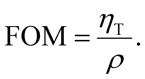 | (2) |
This factor considers the entire range of transmittance in the visible spectrum (from 400 to 800 nm) along with the resistivity (ρ) of the SVO films, which represents an intrinsic property of the material. Importantly, this figure of merit emphasizes sensitivity to both transparency and resistivity, assigning equal significance to both parameters. In contrast to Haacke's method,55 which typically considers only a single point in the visible spectrum (often, the transmittance at λ = 550 nm) raised to the power of 10 and divided by the sheet resistivity, which is thickness dependent. Our figure of merit offers a more comprehensive description of the optoelectronic properties of the films compared to Haacke's method. For the sake of comparison, the as-grown, bare SVO film shows a Haacke FOM of 2.92 × 10⁻⁴ Ω−1, which is lower than most the values reported for epitaxial films in the literature. However, when compared with another studies on non-epitaxial films56 (Fig. S5 in the ESI†), the FOM is in the same range, and even slightly higher. This demonstrates the potential of our approach to make SVO films suitable for industrial applications through their integration on glass substrates and the improvement of their long-term stability.
Fig. 5a presents the FOM for SVO films without and with different capping layers, both before and after aging. On the other hand, Fig. 5b illustrates the ratio between the FOM after aging and before aging. This comparison allows an in-depth evaluation of the efficiency of each capping layer.
 | ||
| Fig. 5 (a) Figure of merit based on the ηT factor and the resistivity of the films. (b) The aging factor, denoted as the ratio between the FOM after aging and the FOM before aging. Both figures (a) and (b) are in logarithmic scale. | ||
Before aging, it is evident that SVO films without protection or those protected with TiO2-based capping layers exhibit a higher figure of merit. This is attributed to the low resistivity and high transparency of these films. However, SVO films protected with Al-based capping layers exhibit a slightly lower figure of merit.
After aging, films protected with Al-based capping layer exhibit the highest figure of merit compared to other capping layers. Moreover, films protected with a-LAO and Al2O3 exhibit a decrease in figure of merit of 19% and 27%, respectively, compared to their values before aging. On the contrary, both unprotected films and those protected with TiO2-based capping layers undergo a significant decline in figure of merit, approaching a reduction of 100%. The substantial degradation in their optical and electronic properties signifies that these films are no longer suitable for use as transparent conducting oxides.
Furthermore, it is essential to note that the focus lies not solely on the figure of merit's value but rather on its variation post-aging, serving as an indicator of the capping layer's efficacy. In our investigation, the observed variability underscores the superior protective performance of Al-based capping layers.
Fig. 6a and b show the real and imaginary parts of dielectric complex permittivity (ε(ω) = ε1(ω) + iε2(ω), ω is the photon angular frequency) of as-grown polycrystalline SVO thin films with different capping layers. The ε1 and ε2 of the as-grown polycrystalline SVO films with and without capping layers, share the same shapes and the same energy positions as the earlier reported results.57 The as-grown polycrystalline SVO films with and without capping layers show a zero crossing of the real part of the dielectric constant at ε1(ω) = 0, extracted from spectroscopic ellipsometry (SE) measurements (as shown the insets in Fig. 6a). It is reported that the zero crossing of ε1(ω) is situated at around ∼1.3 eV for SVO on single crystals, which corresponds to the screened plasma energy  of the material.11,57 The ellipsometry results show that
  of the as-grown polycrystalline SVO samples (Fig. 6a) are dependent on the type of the capping layer. The reference film, i.e. the as-grown unprotected SVO film, has a
  of 1.26 eV. The slightly lower
  obtained in these polycrystalline layers compared to epitaxial films indicate that the films are more transparent in the IR region, and the observed red shift is related to a certain concentration of oxygen vacancies inside the SVO films, leading to a variation of the electronic correlations.15 For the capping layers deposited under vacuum, the observed values are lower for all three samples (1.18 eV for both a-Al2O3 and a-LAO samples, 1.21 eV for a-TiO2-V). This is coherent with the above situation, as the a-LAO, a-Al2O3 and a-TiO2-V capping layers are deposited under vacuum and may attract oxygen ions from the underlying SVO film to achieve a stable stoichiometry, resulting in an even lower
  . For the TiO2-based capping layer grown under oxygen a-TiO2-O,
  = 1.28 eV is higher than for the uncapped SVO film, because of the compensation of oxygen vacancies through the deposition atmosphere of the TiO2, even at such low temperatures (100 °C). Besides the zero crossing of ε1(ω), the enhancement of ε2(ω) at low energies <1 eV observed for all samples is related to the contribution of free charge carriers through the Drude peak, consistent with the conducting nature of the SVO film.
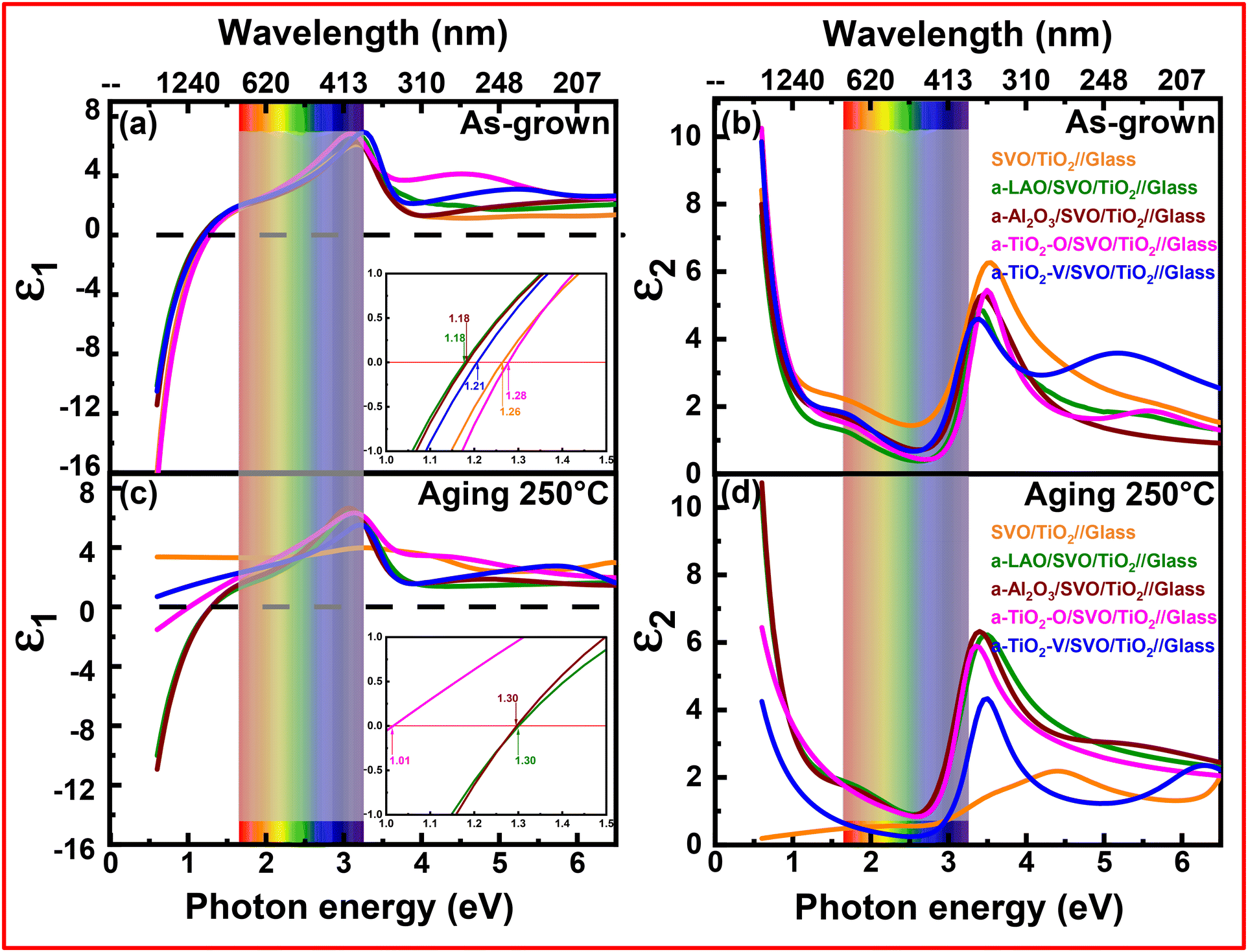 | ||
| Fig. 6 Spectroscopic ellipsometry measurements. (a and b) Real (ε1) and imaginary (ε2) parts of dielectric complex function (ε = ε1 + iε2) of as grown polycrystalline SVO thin films with different capping layers. (c and d) Real and imaginary parts of SVO films with various capping layers’ after annealing for 24 h in air. The inset in (a and c) is a zoom between 1 and 1.5 eV. | ||
After the heat treatment at 250 °C for 24 h, the shape of ε1 and ε2(ω) change fundamentally. The absence of the ε1(ω) = 0 crossing and the flat ε2(ω) evolution at low energies <1 eV shows the absence of free charge carriers, consistent with the insulating nature of the film determined by resistivity measurements. However, the samples with a-Al2O3 (dark red) and a-LAO (dark green) capping layers in Fig. 6c exhibit zero-crossing of ε1(ω) indicating that  increases to reach the bulk value of 1.3 eV. This change confirms the healing of the oxygen vacancies during the heat treatment, already inferred from the slightly enhanced transmittance values in these conducting films. The aging process reduces the number of oxygen vacancies in the SVO film protected with a-LAO and a-Al2O3 and eventually resulting in stoichiometric films. Furthermore, the enhancement of ε2 for a-Al2O3 and a-LAO protected SVO films in the Drude region (i.e. below 1 eV) is consistent with the presence of free charge carriers in these films (Fig. 6d). Hence, the samples with amorphous a-Al2O3 and a-LAO capping layers preserve their electrical as well as transparent properties even after heating at 250 °C for 24 h in air and will perform as a TCOs for optoelectronic applications.
The sample a-TiO2-O (magenta) shows a zero crossing of ε1(ω), but the screened plasma frequency shifts to lower energy (1.01 eV), related to the partial degradation of the SVO film observed by the other characterisations. The Drude contribution of free charges drops correspondingly. The sample a-TiO2-V (blue) shows an even stronger degradation, with a non-negative ε1(ω) value of SVO and an even lower Drude tail, although the contribution does not disappear totally. Hence, after heat treatment, the sample with TiO2 based capping layers behaves as poor electronic conductor, which agrees with the electrical resistivity results (Fig. 2).
To take a closer look at the evolution of the electronic structure of SVO films, we calculated the optical conductivity before and after aging using the following formula:58
| Re(σ(ω)) = ε0ωε2(ω) | (3) |
The calculated real part of the optical conductivity is shown in Fig. 7.
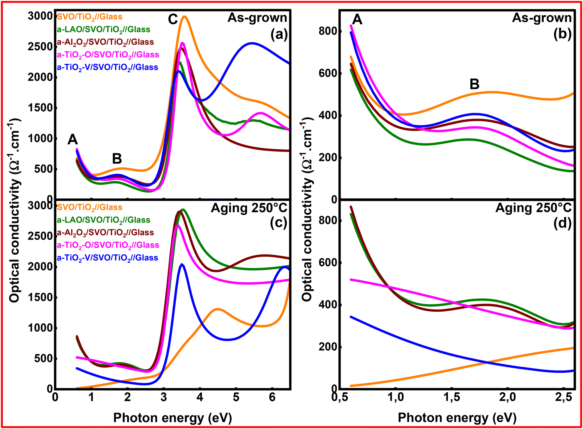 | ||
| Fig. 7 Optical conductivity of as-grown (a and b) and aged at 250 °C (c and d) SVO films capped with different capping layer. (b and d) are a zoom at A and B peaks. | ||
In the as-grown films, the three characteristic peaks of SVO are present, with the first peak (A) corresponding to the Drude contribution. A second peak (B) appears within the range of intermediate energies around 1.7 eV and corresponds to the intraband d–d transitions from the occupied Lower-Hubbard Band (LHB) to the Quasiparticle Band or from the Quasiparticle Band to the unoccupied Upper Hubbard Band (UHB). The third peak (C) appears at higher energies (around 3.5 eV), which corresponds to intraband transitions from the LHB to the UHB, and is situated at twice the energy of Peak B.59,60 The peaks at higher energy correspond to the already mentioned charge transfer transitions from O 2p to V 3d. Regarding the optical conductivity in the Drude region (A) in the as-grown state, the SVO films protected with a-TiO2 layers have the highest optical conductivity. Films protected with a-LAO and a-Al2O3 have the lowest optical conductivity, while the unprotected SVO film shows an intermediate value. After aging, the optical conductivity of this unprotected film approaches zero. Simultaneously, films protected with a-TiO2 capping layers exhibit a significant decrease in optical conductivity. In contrast, films protected with a-LAO and a-Al2O3 layers exhibit an enhancement in the optical conductivity.
Moreover, we observe the suppression of the peak B situated at around 1.7 eV for samples without capping and with a-TiO2 capping layers, indicating the breakdown of the Quasiparticle Band. On the other hand, this peak B of SVO films protected with a-LAO and a-Al2O3 is still observed which confirms the stability of SVO films when protected with Al-based capping layers. These findings align with the observed changes in resistivity over time during the aging process.
Conclusions
This study has focused on the development of efficient capping layers to protect SrVO3 thin films from deterioration in ambient air. A comparative study of various amorphous capping layers, including TiO2 grown in different atmospheres, LAO and Al2O3, has been carried out. Amorphous lanthanum aluminate (a-LAO) and aluminum oxide (a-Al2O3) stand out as the most effective of these capping layers due to their ability to successfully preserve the original state of SVO films without affecting their structural, chemical, electrical, or optical properties. Amorphous TiO2 capping layers proposed earlier46 have shown extremely limited effectiveness compared to the Al-based capping layers, probably because of their limited ability to avoid oxygen diffusion, which leads to the chemical transformation of the conducting SrVO3 phase to over-oxidized V5+ insulating phases. This study not only contributes to the advancement of thin films protection strategies for industrial applications, but also paves the way for enhanced stability and extended lifespan of SVO-based TCOs devices in real conditions.Data availability
The data supporting this article have been included as part of the ESI.†Conflicts of interest
There are no conflicts to declare.Acknowledgements
The authors would like to acknowledge financial support from the CNRS prématuration project CoCOT, and the Normandie region through the projects RIN PLDsurf and Cibox, and the funding of the PhD thesis of M. M.References
- D. S. Ginley and C. Bright, MRS Bull., 2000, 25, 15–18 CrossRef CAS.
- B. G. Lewis and D. C. Paine, MRS Bull., 2000, 25, 22–27 CrossRef CAS.
- H. Liu, V. Avrutin, N. Izyumskaya, Ü. Özgr and H. Morkoç, Superlattices Microstruct., 2010, 48, 458–484 CrossRef CAS.
- E. Fortunato, D. Ginley, H. Hosono and D. C. Paine, MRS Bull., 2007, 32, 242–247 CrossRef CAS.
- A. Stadler, Materials, 2012, 5, 661–683 CrossRef PubMed.
- R. A. Afre, N. Sharma, M. Sharon and M. Sharon, Rev. Adv. Mater. Sci., 2018, 53, 79–89 CAS.
- T. Minami, Semicond. Sci. Technol., 2005, 20, S35–S44 CrossRef CAS.
- L. Alff, P. Komissinskiy, A. Radetinac, T. Sirman and M. Vafaee, J. Phys. D:Appl. Phys., 2014, 47, 034012 CrossRef CAS.
- A. Radetinac, A. Mani, S. Melnyk, M. Nikfalazar, J. Ziegler, Y. Zheng, R. Jakoby, L. Alff and P. Komissinskiy, Appl. Phys. Lett., 2014, 105, 114108 CrossRef.
- A. Radetinac, J. Zimmermann, K. Hoyer, H. Zhang, P. Komissinskiy and L. Alff, J. Appl. Phys., 2016, 119, 055302 CrossRef.
- L. Zhang, Y. Zhou, L. Guo, W. Zhao, A. Barnes, H. T. Zhang, C. Eaton, Y. Zheng, M. Brahlek, H. F. Haneef, N. J. Podraza, M. H. W. Chan, V. Gopalan, K. M. Rabe and R. Engel-Herbert, Nat. Mater., 2016, 15, 204–210 CrossRef CAS PubMed.
- Y. Ha and S. Lee, Adv. Funct. Mater., 2020, 30, 1–8 CrossRef.
- Y. Park, J. Roth, D. Oka, Y. Hirose, T. Hasegawa, A. Paul, A. Pogrebnyakov, V. Gopalan, T. Birol and R. Engel-Herbert, Commun. Phys., 2020, 3, 1–7 CrossRef.
- A. Boileau, A. Cheikh, A. Fouchet, A. David, C. Labbé, F. Gourbilleau, U. Lüders, A. Boileau, A. Cheikh, A. Fouchet and A. David, Appl. Phys. Lett., 2018, 112, 021905 CrossRef.
- A. Boileau, A. Cheikh, A. Fouchet, A. David, C. Labbé, P. Marie, F. Gourbilleau and U. Lüders, Adv. Opt. Mater., 2019, 7, 1801516 CrossRef.
- M. Mirjolet, H. B. Vasili, L. López-Conesa, S. Estradé, F. Peiró, J. Santiso, F. Sánchez, P. Machado, P. Gargiani, M. Valvidares and J. Fontcuberta, Adv. Funct. Mater., 2019, 29, 1–11 Search PubMed.
- D. H. Jung, H. S. So and H. Lee, J. Vac. Sci. Technol., A, 2019, 37, 021507 CrossRef.
- A. Boileau, S. Hurand, F. Baudouin, U. Lüders, M. Dallocchio, B. Bérini, A. Cheikh, A. David, F. Paumier, T. Girardeau, P. Marie, C. Labbé, J. Cardin, D. Aureau, M. Frégnaux, M. Guilloux-Viry, W. Prellier, Y. Dumont, V. Demange and A. Fouchet, Adv. Funct. Mater., 2022, 32, 2108047 CrossRef CAS.
- M. Mohammadi, R. Xie, N. Hadaeghi, A. Radetinac, A. Arzumanov, P. Komissinskiy, H. Zhang and L. Alff, Adv. Mater., 2023, 35, 2206605 CrossRef CAS PubMed.
- A. Cheikh, O. El khaloufi, M. Rath, U. Lüders, A. Fouchet, J. Cardin, C. Labbé, W. Prellier and A. David, ACS Appl. Mater. Interfaces, 2024, 16, 47854–47865 CrossRef CAS PubMed.
- C. G. Granqvist and A. Hultåker, Thin Solid Films, 2002, 411, 1–5 CrossRef CAS.
- J. Macías, A. A. Yaremchenko and J. R. Frade, J. Alloys Compd., 2014, 601, 186–194 CrossRef.
- J. Macías, A. A. Yaremchenko, D. P. Fagg and J. R. Frade, Phys. Chem. Chem. Phys., 2015, 17, 10749–10758 RSC.
- B. Bérini, V. Demange, M. Bouttemy, E. Popova, N. Keller, Y. Dumont and A. Fouchet, Adv. Mater. Interfaces, 2016, 3, 6–11 Search PubMed.
- X. J. Gu, Z. L. Luo, Y. Q. Dong, J. T. Zhou, H. Xu, B. Hong and C. Gao, Chin. J. Chem. Phys., 2019, 32, 727–730 CrossRef CAS.
- V. Polewczyk, M. Mezhoud, M. Rath, O. El-Khaloufi, F. Bassato, A. Fouchet, W. Prellier, M. Frégnaux, D. Aureau, L. Braglia, G. Vinai, P. Torelli and U. Lüders, Adv. Funct. Mater., 2023, 33, 2301056 CrossRef CAS.
- M. Rath, M. Mezhoud, O. El Khaloufi, O. Lebedev, J. Cardin, C. Labbé, F. Gourbilleau, V. Polewczyk, G. Vinai, P. Torelli, A. Fouchet, A. David, W. Prellier and U. Lüders, ACS Appl. Mater. Interfaces, 2023, 15, 20240–20251 CrossRef CAS PubMed.
- R. C. Germanicus, Y. Bourlier, V. Notot, B. Bérini, V. Demange, M. Berthe, A. Boileau, M. Euchin, Y. Dumont, D. Aureau, M. Fregnaux, B. Grandidier, U. Lüders, A. David, W. Prellier, L. Biadala and A. Fouchet, Appl. Surf. Sci., 2020, 510, 145522 CrossRef CAS.
- Y. Bourlier, M. Frégnaux, B. Bérini, A. Fouchet, Y. Dumont and D. Aureau, ChemNanoMat, 2019, 5, 674–681 CrossRef CAS.
- Y. Bourlier, B. Bérini, M. Frégnaux, A. Fouchet, D. Aureau and Y. Dumont, ACS Appl. Mater. Interfaces, 2020, 12, 8466–8474 CrossRef CAS PubMed.
- P. Salg, L. Zeinar, A. Radetinac, D. Walk, H. Maune, R. Jakoby, L. Alff and P. Komissinskiy, J. Appl. Phys., 2020, 127, 065302 CrossRef CAS.
- S. Thapa, S. R. Provence, P. T. Gemperline, B. E. Matthews, S. R. Spurgeon, S. L. Battles, S. M. Heald, M. A. Kuroda and R. B. Comes, APL Mater., 2022, 10, 091112 CrossRef CAS.
- N. Tsvetkov, Q. Lu, L. Sun, E. J. Crumlin and B. Yildiz, Nat. Mater., 2016, 15, 1010–1016 CrossRef CAS PubMed.
- B. Koo, K. Kim, J. K. Kim, H. Kwon, J. W. Han and W. C. Jung, Joule, 2018, 2, 1476–1499 CrossRef CAS.
- M. Choi, I. A. M. Ibrahim, K. Kim, J. Y. Koo, S. J. Kim, J. W. Son, J. W. Han and W. Lee, ACS Appl. Mater. Interfaces, 2020, 12, 21494–21504 CrossRef CAS PubMed.
- H. Li, Y. Chen, J. Z. Y. Seow, C. Liu, A. C. Fisher, J. W. Ager and Z. J. Xu, Small Sci., 2022, 2, 2100048 CrossRef CAS PubMed.
- S. Valencia, Z. Konstantinovic, D. Schmitz, A. Gaupp, L. Balcells and B. Martínez, Phys. Rev., 2011, 84, 1–7 Search PubMed.
- N. Li, H. Dong, H. Dong, J. Li, W. Li, G. Niu, X. Guo, Z. Wu and L. Wang, J. Mater. Chem. A, 2014, 2, 14973–14978 RSC.
- Y. Wu, Y. Wei, Y. Huang, F. Cao, D. Yu, X. Li and H. Zeng, Nano Res., 2017, 10, 1584–1594 CrossRef CAS.
- S. Lin, Q. Zhang, M. A. Roldan, S. Das, T. Charlton, M. R. Fitzsimmons, Q. Jin, S. Li, Z. Wu, S. Chen, H. Guo, X. Tong, M. He, C. Ge, C. Wang, L. Gu, K. J. Jin and E. J. Guo, Phys. Rev. Appl., 2020, 13, 1 CrossRef.
- E. K. Ko, J. Mun, H. G. Lee, J. Kim, J. Song, S. H. Chang, T. H. Kim, S. B. Chung, M. Kim, L. Wang and T. W. Noh, Adv. Funct. Mater., 2020, 30, 1–10 Search PubMed.
- S. Thomas, B. Kuiper, J. Hu, J. Smit, Z. Liao, Z. Zhong, G. Rijnders, A. Vailionis, R. Wu, G. Koster and J. Xia, Phys. Rev. Lett., 2017, 119, 1–5 Search PubMed.
- D. J. Baek, D. Lu, Y. Hikita, H. Y. Hwang and L. F. Kourkoutis, ACS Appl. Mater. Interfaces, 2017, 9, 54–59 CrossRef CAS PubMed.
- D. Li, C. Adamo, B. Y. Wang, H. Yoon, Z. Chen, S. S. Hong, D. Lu, Y. Cui, Y. Hikita and H. Y. Hwang, Nano Lett., 2021, 21, 4454–4460 CrossRef CAS PubMed.
- D. Kumar, A. Fouchet, A. David, A. Cheikh, T. S. Suraj, O. Copie, C. U. Jung, A. Pautrat, M. S. Ramachandra Rao and W. Prellier, Phys. Rev. Mater., 2019, 3, 1–9 CAS.
- S. Caspi, L. Shoham, M. Baskin, K. Weinfeld, C. Piamonteze, K. A. Stoerzinger and L. Kornblum, J. Vac. Sci. Technol., A, 2022, 40, 013208 CrossRef CAS.
- A. Cohen, M. Baskin, L. Shoham, S. Caspi, P. Shekhter, T. L. Lee, S. A. Chambers and L. Kornblum, Appl. Phys. Lett., 2025, 126, 161602 CrossRef CAS.
- M. Upadhyay, PhD thesis, Normandie Université, 2021.
- R. Schaub, E. Wahlström, A. Rønnau, E. Lægsgaard, I. Stensgaard and F. Besenbacher, Science, 2003, 299, 377–379 CrossRef CAS PubMed.
- A. Rothschild, F. Edelman, Y. Komem and F. Cosandey, Sens. Actuators, B, 2000, 67, 282–289 CrossRef CAS.
- G. S. Herman, R. T. Zehr and M. A. Henderson, Surf. Sci., 2013, 612, L5–L8 CrossRef CAS.
- A. V. Bakulin, E. V. Matyskina and S. E. Kulkova, AIP Conf. Proc., 2022, 2509, 020016 CrossRef CAS.
- S. Guarnera, A. Abate, W. Zhang, J. M. Foster, G. Richardson, A. Petrozza and H. J. Snaith, J. Phys. Chem. Lett., 2015, 6, 432–437 CrossRef CAS PubMed.
- S. Lange, T. Arroval, R. Saar, I. Kink, J. Aarik and A. Krumme, Polym.-Plast. Technol., 2015, 54, 301–304 CrossRef CAS.
- G. Haacke, J. Appl. Phys., 1976, 47, 4086–4089 CrossRef CAS.
- P. T. P. Le, S. Ni, P. A. Repecaud, E. van der Minne, K. J. H. Van Den Nieuwenhuijzen, M. D. Nguyen, J. E. ten Elshof, M. Morales-Masis and G. Koster, Adv. Mater. Interfaces, 2023, 10, 1–8 Search PubMed.
- M. Mirjolet, F. Sánchez and J. Fontcuberta, Adv. Funct. Mater., 2019, 29, 1808432 CrossRef.
- Y. Ha, J. Byun, J. Lee and S. Lee, Laser Photonics Rev., 2021, 15, 1–7 Search PubMed.
- H. Makino, I. H. Inoue, M. J. Rozenberg, I. Hase, Y. Aiura and S. Onari, Phys. Rev. B:Condens. Matter Mater. Phys., 1998, 58, 4384 CrossRef CAS.
- L. Shoham, M. Baskin, T. Tiwald, G. Ankonina, M. G. Han, A. Zakharova, S. Caspi, S. Joseph, Y. Zhu, I. H. Inoue, C. Piamonteze, M. J. Rozenberg and L. Kornblum, Adv. Funct. Mater., 2023, 33, 2302330 CrossRef CAS.
Footnote |
| † Electronic supplementary information (ESI) available. See DOI: https://doi.org/10.1039/d4nr04806g |
| This journal is © The Royal Society of Chemistry 2025 |