
 Open Access Article
 This Open Access Article is licensed under a Creative Commons Attribution-Non Commercial 3.0 Unported Licence
Exciton–phonon coupling in quasi-two-dimensional Ruddlesden–Popper perovskites: impact of a mixed-phase structure†
Sushovan
Sarkar
ab,
Nagendra S.
Kamath
ab,
Koushik
Gayen
ab and
Suman Kalyan
Pal
 *ab
*ab
aSchool of Physical Sciences, Indian Institute of Technology Mandi, Kamand, Mandi-175005, Himachal Pradesh, India. E-mail: suman@iitmandi.ac.in; Tel: +91 1905 267040
bAdvanced Materials Research Centre, Indian Institute of Technology Mandi, Kamand, Mandi-175005, Himachal Pradesh, India
First published on 25th March 2025
Abstract
Two-dimensional (2D) metal halide perovskites (MHPs) hold great potential for optoelectronic and spintronic device applications due to their outstanding optical and electronic properties. In this study, we conducted a systematic temperature-dependent photoluminescence (PL) investigation to elucidate the influence of exciton–phonon scattering on the optoelectronic properties of 2D Ruddlesden–Popper (RP) perovskites, (C6H7SNH3)2 (CH3NH3)n−1PbnI3n+1 (n = 1–4). The results from our micro-PL study suggest that the optical band gap of each 2D phase (a perovskite with a specific number of inorganic layers, n) varies with temperature due to thermal lattice expansion and exciton–phonon interactions. The strength of exciton–phonon interactions differs in each 2D phase within a mixed-phase sample, with a notable increase as the layer number (n) rises. This enhancement is attributed to greater lattice mismatch, increased interface complexity, and a higher degree of disorder within the system. Additionally, we found that parameters such as exciton–phonon coupling strength and exciton binding energy exhibit significantly different behaviours across various mixed-phase perovskite samples, likely due to changes in the local environment around excitons in each specific phase. These findings offer valuable insights into the mechanisms underlying nonradiative processes and scattering phenomena and provide guidance for optimizing the efficiency of 2D-RP mixed-phase perovskite-based optoelectronic and spintronic devices.
1. Introduction
Organic–inorganic metal halide perovskites (OIMHPs) are rapidly emerging as the shining stars in the realm of optoelectronics due to their excellent electrical and optical properties such as tunable bandgap, high light absorption coefficient, high defect tolerance, long charge carrier diffusion length, and high photoluminescence (PL) quantum yield.1–5 Due to these superior optoelectronic properties, OIMHPs have shown great promise for photovoltaics, light-emitting diodes, lasers and photodetectors.6–10 Moreover, OIMHPs exhibit exceptional spin-dependent photophysical properties due to giant spin–orbital coupling (SOC) in heavy lead (Pb) atoms and interactions between spin–orbit and electron–hole exchange.11,12 This suggests that OIMHPs are also promising materials for next-generation spintronic devices and have generated great research interest on perovskite spintronics. However, three-dimensional (3D) perovskites face inherent instability when exposed to ambient conditions, posing a barrier to their widespread practical utilization.13 In this regard, extensive recent research has focused on two-dimensional (2D) layered Ruddlesden–Popper (RP) perovskites as a notably stable substitute for their 3D counterparts because of the presence of terminal hydrophobic large aliphatic or aromatic alkylammonium cations within the structure.14,15The general formula of 2D-RP lead halide perovskites is (A′)2(A)n−1PbnX3n+1, where A′ is a monovalent long chain organic spacer cation, A is a monovalent small organic or inorganic cation, X is a halide anion and n denotes a positive integer indicating the number of inorganic layers sandwiched between two layers of A′ spacer cations.16 These structures represent atomically thin 2D quantum wells composed of [PbX6]4− octahedral sheets separated by organic chains (Fig. 1a) and bound together by van der Waals forces. By adjusting the chemical compositions and layer number (n), it is possible to finely modulate the optical band gap of the material across a broad spectrum, ranging from violet to near-infrared wavelengths.17 The organic chain A′ acts as a dielectric layer with a lower dielectric constant compared to the inorganic layer.18 This difference results in a substantial exciton binding energy (EBE) due to dielectric confinement, offering significant potential for applications in polaritonic devices.19 Additionally, RP halide perovskites have been found to exhibit various photophysical processes, including biexciton formation, exciton–exciton annihilation, edge-state formation, self-trapping of excitons, and spin-related phenomena such as Rashba and Dresselhaus splitting, the optical Stark effect (OSE) and the magneto-optical effect, which make them suitable for optoelectronic and spintronic applications.20–26 However, the performance of such devices is contingent upon several factors. In optoelectronic devices, efficiency is influenced by exciton dissociation, emission linewidth, and carrier relaxation time.27 On the other hand, for spintronic devices, essential factors include the time of spin flips and spin relaxation via momentum scattering and spin decoherence time, all of which are mainly regulated by phonon scattering mechanisms.28,29 It has been reported that both the size of the organic cation species and the quantity of inorganic octahedral layers play crucial roles in determining the excitonic properties and carrier dynamics of 2D perovskites.30,31 In 2016, Guo et al. explored exciton relaxation mechanisms and phonon scattering in ultrathin single exfoliated flakes of 2D-RP perovskites by analyzing temperature-dependent PL dynamics.32 Li and co-workers investigated the effects of thermal expansion and electron–phonon interactions in phase-pure 2D-RP perovskites by examining how the optical band gap evolves with temperature.33 Recently, Ye's group reported on the phenomenon of electron–phonon coupling in pure-phase 2D single crystals with different organic cations and inorganic layers by observing the broadening of emission linewidths.34 However, these previous studies primarily focus on the carrier phonon interactions within phase-pure 2D-RP perovskite systems only. On the other hand, it has been generally observed that solution-processed RP-type 2D perovskite samples tend to exhibit mixed-phase (phases with different n values) characteristics due to comparable phase formation energies.15 To date, there have been limited reports on exciton–phonon coupling in mixed-phase RP perovskite systems. A thorough and comparative analysis of phonon scattering across different phases within mixed-phase perovskites remains absent in the literature. Hence, comprehending the influence of the layer number (n) on exciton–phonon interactions in mixed-phase 2D-RP perovskites is crucial not only for advancing fundamental research but also for enhancing their efficiency in optoelectronic and spintronic applications.
 | ||
| Fig. 1 (a) Schematic structures of the 2D RP perovskites, (TEA)2(MA)n−1PbnI3n+1 (n = 1–4). (b) Absorption spectra of the 2D RP perovskite films (S1–S4). | ||
In this study, we present a systematic investigation of exciton–phonon coupling in mixed-phase 2D-RP perovskites (TEA)2(MA)n−1PbnI3n+1 (n = 1–4) by temperature-dependent PL spectroscopy. We examined variations in PL intensity, spectral shifts, and linewidth broadening of the samples as functions of temperature which is a consequence of exciton–phonon scattering. As the temperature decreases, the PL intensities of all peaks enhance, while linewidths become narrower, attributed to the suppression of optical phonons. Additionally, the degree of phonon scattering increases with increasing number of inorganic layers due to more lattice mismatches and grain boundary scattering. Furthermore, the EBE, strength of phonon scattering and other related parameters corresponding to a particular phase exhibit significantly different behaviors across mixed-phase samples. This discrepancy is ascribed to changes in the surrounding environment of excitons and alterations in the electronic structure. Our experimental findings with qualitative and quantitative interpretations provide a comprehensive understanding of exciton–phonon scattering within mixed-phase 2D-RP perovskites.
2. Experimental section
2.1 Materials
The chemicals 2-thiopheneethylamine (C6H7SNH2 (TEA), 98%), methyl ammonium iodide (CH3NH3I (MAI), 99.9%), lead iodide (PbI2, 99.999% purity, metals basis), dimethylformamide (DMF), hydroiodic acid (HI, 57%), dimethyl sulfoxide (DMSO), isopropyl alcohol (IPA), ethanol, diethyl ether and acetone were obtained from Sigma-Aldrich. These chemicals were employed as received without any further purification.2.2 Synthesis of 2-thiopheneethylamine iodide (TEAI) salt
TEAI salt was synthesized via the reaction between TEA and HI. Equimolar quantities of TEA and HI were dissolved in ethanol and subjected to stirring for 3 h. Subsequently, this solution was subjected to rotary evaporation under controlled conditions at 60 °C. The resulting TEAI salts were redissolved in an ethanol solution and subjected to multiple washes with diethyl ether. Finally, white crystals were obtained after drying at 60 °C for 6 h and stored within N2 gas filled glove box for further use.2.3 Preparation of precursor solutions
The precursor solutions were prepared to facilitate the synthesis of perovskite materials. Different precursor solutions were prepared according to their stoichiometric ratios. For the case of (TEA)2PbI4, 0.2 mmol of TEAI and 0.1 mmol of PbI2 were dissolved, whereas for (TEA)2MAPb2I7, the precursor solution comprised 0.2 mmol of TEAI, 0.1 mmol of MAI, and 0.2 mmol of PbI2. Similarly, for (TEA)2MA2Pb3I10, the solution consisted of 0.2 mmol of TEAI, 0.2 mmol of MAI, and 0.3 mmol of PbI2, while for (TEA)2MA3Pb4I13, the solution included 0.2 mmol of TEAI, 0.3 mmol of MAI, and 0.4 mmol of PbI2. These salts were dissolved in a mixture solvent composed of 900 μL of DMF and 100 μL of DMSO.2.4 Preparation of perovskite films
Quartz substrates were subjected to a multi-step cleaning process involving sequential immersion in detergent water, deionized (DI) water, acetone, and IPA within an ultrasonic bath for a duration of 10 min each. Subsequently, the substrates were subjected to UV/ozone treatment for 20 min. Perovskite films were fabricated via spin coating onto the treated quartz substrates at a speed of 4000 rpm for 20 s, followed by annealing at 120 °C for 5–6 min. We prepared four types of samples (S1–S4) to obtain 2D and quasi-2D perovskite phases: (TEA)2PbI4 in S1, (TEA)2MAPb2I7 in S2, (TEA)2MA2Pb3I10 in S3, and (TEA)2MA3Pb4I13 in S4.2.5 Characterization
X-ray diffraction (XRD) patterns of the (TEA)2(MA)n−1PbnI3n+1 (n = 1–4) perovskite films were obtained using a Rigaku MiniFlex diffractometer. Steady-state UV-visible absorption spectra were recorded using a Shimadzu UV-2700 spectrometer. Temperature-dependent PL measurements were carried out in a home-build low-temperature micro-PL setup. In this setup, a microscope objective (5× and 0.15 NA) was used for the collection of PL and spectra were recorded using a charge-coupled device (CCD) detector with 600 groves mm−1 from Ocean optics (USB4000). To vary the sample temperature, a temperature-controlled heating stage from Linkam (LTS420E-PB4) was used. Current–voltage (I–V) measurements were performed using a programmable source meter (Keithley 2400). PL decay for all samples was measured using a Horiba Fluorolog-QM system with a pulsed 400 nm laser as the excitation source.3. Results and discussion
The structures of the prepared 2D perovskites, (TEA)2(MA)n−1PbnI3n+1 (n = 1–4), are schematically shown in Fig. 1(a). Thin-film XRD patterns, as shown in Fig. S1,† demonstrate the highly crystalline nature of the spin-coated RP perovskite films. For S1, the XRD pattern displays a sharp and intense diffraction peak at 2θ ≈ 6.2°, indicating the presence of a pure 2D phase.35 The intense lower-angle diffraction peak shifts at 2θ ≈ 4.8° in the S2 sample, which is a direct consequence of the increased interlayer distance due to the incorporation of more inorganic layers. However, the appearance of a low intense peak at diffraction angle of 6.1° for S2 indicates that a pure 2D phase perovskite material is also present. Furthermore, in S2 and S3, the XRD patterns exhibit distinct peaks at ≈14.8° and 29° that are indicative of the 3D perovskite phase.36 Moreover, the presence of diffraction peaks of S2 in the XRD pattern of S3 suggests the coexistence of mixed phases. The characteristic peak of the low-dimensional perovskite gradually diminishes from samples S2 to S4, reflecting the transition to a more quasi-2D structure. For S4, the XRD pattern shows more pronounced diffraction peaks of the 3D phase at ≈14.8° and 29°. The XRD results indicate that S1 consists of a pure 2D phase (n = 1), while the S2–S4 are mixed-phase samples contain both 2D phases (n = 1–4) and bulk phases.Fig. 1(b) shows the absorption spectra of the 2D perovskite films (S1–S4) at room temperature. The absorption spectra reveal that sample S1 exhibits a distinct peak at 2.39 eV, whereas additional peaks are observed at 2.18, 2.03, and 1.92 eV in each of samples S2–S4. Based on previous studies of similar kinds of perovskite materials, the absorption peaks observed at 2.39 eV (519 nm), 2.18 eV (569 nm), 2.03 eV (611 nm) and 1.92 eV (646 nm) correspond to the different-layered phases from n = 1 to 4, respectively.28,30,37 These observations infer that a combination of phases (n = 1–4) are present in our quasi-2D (n > 1) lead halide perovskite samples. Though the films were prepared following the standard formula for each phase, coexistence of a mixed phase arises because the formation energies of the different phases are comparable.15 As anticipated, the absorption peaks exhibit a consistent blue-shift from n = 4 to n = 1, which is attributed to the increase in the optical band gap as n decreases. As the inorganic layers become thinner, charge carriers are quantum mechanically confined in the direction perpendicular to the plane, increasing the distance between energy levels and consequently enlarging the optical band gap.38 In a pure 2D perovskite, the exciton state is localized (Frenkel-type) perpendicular to the layer and delocalized (Wannier-type) in the layer.39 As the number of perovskite layers n increases, excitons gradually spread out between the PbX42− layers, transitioning from a localized Frenkel-type to a delocalized Wannier-type state at the 3D limit. Therefore, the rise in the optical band gap is partially offset by the increase in the EBE as the layer number decreases from 4 to 1 which can be attributed to the reduced dielectric screening strength. The combination of these two phenomena results in the differences depicted in the absorption behavior of the samples (Fig. 1(b)).
To explore exciton–phonon scattering in the 2D perovskites, we conducted temperature-dependent micro-PL measurements across the temperature range of 83–298 K. The excitation wavelength (energy) used in the micro-PL study was 405 nm (3.06 eV) for S1 while for S2–S4, a 532 nm (2.33 eV) laser was utilized for excitation. We have fine-tuned the excitation power across the entire measurement range to ensure that it remains below the threshold for detector saturation, particularly within the lower temperature range. Fig. 2(a–d) illustrate the variation of PL intensity and peak position as a function of temperature for the perovskite samples with n values ranging from 1 to 4. The PL spectra indicate distinct spectral characteristics among the samples. Sample S1 displays a prominent peak at approximately 2.36 eV, whereas sample S2 exhibits multiple peaks centered at around 2.14, 1.99, and 1.91 eV. Conversely, samples S3 and S4 feature an additional peak observed at around 1.6 eV compared to sample S2. Similar to the absorption spectra, the PL spectra of S2–S4 provide evidence for the coexistence of different-layered phases in the quasi-2D perovskite samples. According to earlier studies on similar materials, the observed peaks at 2.36 eV (526 nm), 2.14 eV (580 nm), 1.99 eV (621 nm) and 1.91 eV (650 nm) are attributed to the phases from n = 1 to n = 4, respectively.7,30,32,40 The additional peak in S3 and S4 at 1.6 eV (775 nm) reflect the characteristics of 3D lead iodide perovskites.41,42
 | ||
| Fig. 2 Temperature-dependent PL spectra of the (TEA)2(MA)n−1PbnI3n+1 thin films at different temperatures from 83 to 298 K. Panels (a–d) correspond to samples S1–S4, respectively. The excitation wavelengths were 405 nm for S1 and 532 nm for S2–S4. | ||
To precisely ascertain the underlying origins of these peaks, we conducted excitation power-dependent PL measurements at 83 K, as depicted in Fig. S2,† and extracted the emission intensity under each peak using the multiple peak fitting technique. To systematically analyze the data, we have deconvoluted all the PL spectra using the Lorentzian function. The PL intensities of all peaks were plotted as a function of excitation power and fitted with the relationship, I ∝ Pm (where I is the PL intensity and P is the excitation power) (Fig. S3†). It is found that all the peaks show a super linear (m∼1) relationship with the excitation power which reflects the excitonic emission behavior.43 We must mention that this study primarily concentrates on the principal PL peak of each sample (i.e., for n = 1 at 2.36 eV of S1, n = 2 at 2.14 eV of S2, n = 3 at 1.99 eV of S3 and n = 4 at 1.91 eV of S4). However, a detailed analysis of other peaks of all the samples are also provided in the ESI.†
As shown in Fig. 2(a–d), the PL intensities of all the samples increase as the temperature decreases from room temperature to 83 K. At higher temperatures, the thermal energy of the materials increases which promotes phonon-mediated non-radiative processes, such as phonon scattering and phonon-assisted recombination. As the temperature decreases, the scattering of excitons by lattice vibration minimizes due to the reduction in thermal energy. Consequently, the non-radiative processes such as phonon-assisted transition, defect-related processes and exciton–phonon coupling are suppressed. As a result, more excitons are allowed to undergo radiative recombination, leading to increased PL intensity. After careful observation, one can find that the primary PL peak splits into two distinct peaks below 140 K for the S1 sample and 200 K for the S2 and S3 samples (Fig. 2(a–c)). At 83 K, a single emission peak accompanied by a secondary lower-energy shoulder has been observed for the S1, S2 and S3 samples, which is attributed to the coexistence of the high and low temperature phases and phonon replica and/or self-trapped states.44,45 On the other hand, only one emission peak corresponding to the n = 4 phase in S4 is present, arising mainly from the free carrier recombination. It should be noted that though there is a coexistence of multiple phases in the quasi-2D (n > 1) samples, the PL peak dominates in samples S2 and S3 are for n = 2 and n = 3, respectively (Fig. 2(b and c)). It is evident from the PL spectra (Fig. 2(c and d)) that in S3, the bulk features are induced and notably more pronounced compared to other peaks in the S4 sample due to the greater incorporation of MA for the synthesis of quasi-2D perovskites with higher n. As a result, the photoexcited carriers can be transferred from the higher excited states to the available lower bulk energy level via phonon scattering.46 Hence, for this charge transfer process, the PL intensity of the peak corresponding to the n = 4 phase in the S4 sample is notably diminished. The temperature evolution of the peak corresponding to the 3D bulk perovskite phase at around 1.6 eV is very similar to that of the previous report.42 However, the detailed analysis of the bulk characteristics is beyond the interest of this study.
In 2D MHPs, excitonic recombination is the source of the measured PL and the increase in the thermal dissociation rate of excitons at higher temperatures is the reason for the decrease in PL intensity. The increasing temperature can supply the necessary activation energy to trigger the dissociation of excitons, creating a competition with radiative excitonic recombination processes.47 Therefore, we can determine the activation energy required for exciton dissociation, which is nothing but the EBE, by monitoring the variation in PL emission intensity with temperature. The temperature (T) dependency of integrated PL intensity I(T) can be elucidated by utilization of the Arrhenius equation:48
 | (1) |
 | ||
| Fig. 3 Inverse of integrated PL intensity [1/I(T)] vs. inverse of temperature (1/T) plots fitted (solid lines) using eqn (1) for (a) S1, (b) S2, (c) S3 and (d) S4. | ||
The comprehensive details regarding the best fit parameters of 1/I(T) vs. 1/T plots for other peaks of samples S2–S4 are shown in Fig. S4 and Table S1.† The EBE is nothing but the electrostatic potential energy that arises from the interaction between the photoexcited electrons and holes. As more inorganic layers are added, the electrons and holes become farther apart, diminishing their coulombic interaction energy and consequently lowering the EBE. Moreover, with increasing number of inorganic layers the width of the inorganic well with higher dielectric constant also expands, which further weakens the EBE due to enhanced dielectric screening effects. Interestingly, the EBE corresponding to a particular phase decreases as one moves from S2 to S4 (Table S1†). Although there are mixed phases in samples S2–S4, they may be formed in different proportions because the organic and inorganic salts are used in different stoichiometries for preparing these samples. As a result, the local environment of excitons associated with a particular phase varies across different mixed-phase samples.
The PL peak positions exhibit distinct variations with the temperature in different 2D perovskite phases (Fig. 4). In the case of the n = 1 phase of S1, the PL peak shows a gradual blue shift as the temperature increases from 83 to 298 K with a deep between 240 and 260 K (Fig. 4(a)). The sudden red shift at 240 K could be attributed to orthorhombic to orthorhombic phase transition.49 As the temperature increases from 83 K, the emission peak initially undergoes a consistent blue shift followed by a subsequent red shift for the n = 2 and 3 phases of the S2 and S3 films (Fig. 4(b and c)). Therefore, a structural phase transition may occur for these phases between 190 and 220 K. As shown in Fig. 4(d), for the n = 4 phase (of S4), there is a minimal increase in the peak energy at low temperatures and the emission peak shows a monotonic red shift with the increase of temperature followed by a phase transition at around 200–220 K. These findings suggest that the temperature-dependent emission behavior of different 2D phases is intrinsic in nature. However, the exceptional blue shift of PL emission in perovskites with an increase in the temperature cannot be explained by the Varshini model, which is frequently employed for describing the typical red shift of PL emission in conventional semiconductors due to lattice dilation with increasing temperature.47,50 It is noteworthy that in typical semiconductors, the conduction band minima (CBM) and the valence band maxima (VBM) are determined by the bonding and antibonding orbital pairs between atoms. Consequently, when the lattice is stretched, it causes a widening effect on these orbitals, resulting in a reduction of the energy gap between the VBM and the CBM.51 In contrast, for MHPs, a strong s–p antibonding interaction between Pb and I form the VBM while the CBM is primarily shaped by the bonding orbital states of lead's 6p electrons. As a result, lattice dilation causes the VBM energy to decrease while the CBM energy marginally increases. Consequently, the optical band gap of MPHs shifts towards higher energies, exhibiting a blue-shift with increasing temperature, as observed in this study.52
 | ||
| Fig. 4 (a–d) Evolution of the PL peak position as a function of temperature for the n = 1–4 phases, respectively, of (TEA)2(MA)n−1PbnI3n+1. | ||
According to the previous literature, thermal expansion of the lattice and exciton–phonon interaction are the two ways in which temperature influences the emission peak or optical band gap (Eg).53,54 Thermal expansion modifies the lattice constant, thereby directly affecting the electronic bands, while exciton–phonon interaction induces lattice vibrations influencing the electronic band structure.54,55 The temperature-dependent behavior of the optical band gap, under constant pressure and utilizing a quasi-harmonic approximation, can typically be described as follows:55,56
 | (2) |
 is the number of phonons at the j branch with the wave vector
  and follows the Bose–Einstein distribution. The first part of eqn (2) reflects the thermal expansion of the lattice which arises due to the anharmonicity in the potentials between atoms, while the second term denotes the impact of exciton–phonon interaction on the system. It is nearly hard to calculate the second term of eqn (2) exactly because it comprises all phonon modes that might possibly exist throughout the whole Brillouin zone.53 In practice, only a limited number of phonon modes are typically taken into account and numerous models have been considered to elucidate the experimental findings in relationship to the number of dominant phonon modes that play a significant role in the optical band gap evolution.54,56 Among these models, the two-oscillator model is a commonly employed approach for interpreting the temperature-dependent evolution in the optical band gap, which takes into account only one branch of the acoustic and optical phonons. According to previous reports, the temperature evolution of the optical band gap in 3D perovskites is better described by the one-oscillator model.56 For our 2D perovskite within the temperature range of 83–298 K, the primary influence on exciton–phonon interaction arises from longitudinal optical (LO) phonon scattering through Fröhlich coupling and the contribution from acoustic phonon scattering is insignificant.57,58 Hence, we opted for the one-oscillator model for our subsequent analysis. If we make the assumption that there is a direct correlation between the lattice constant and the temperature along with the one-oscillator model we discussed above, eqn (2) can be expressed as,53,55,56
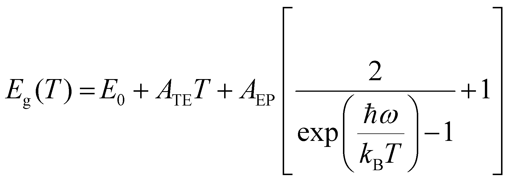 | (3) |
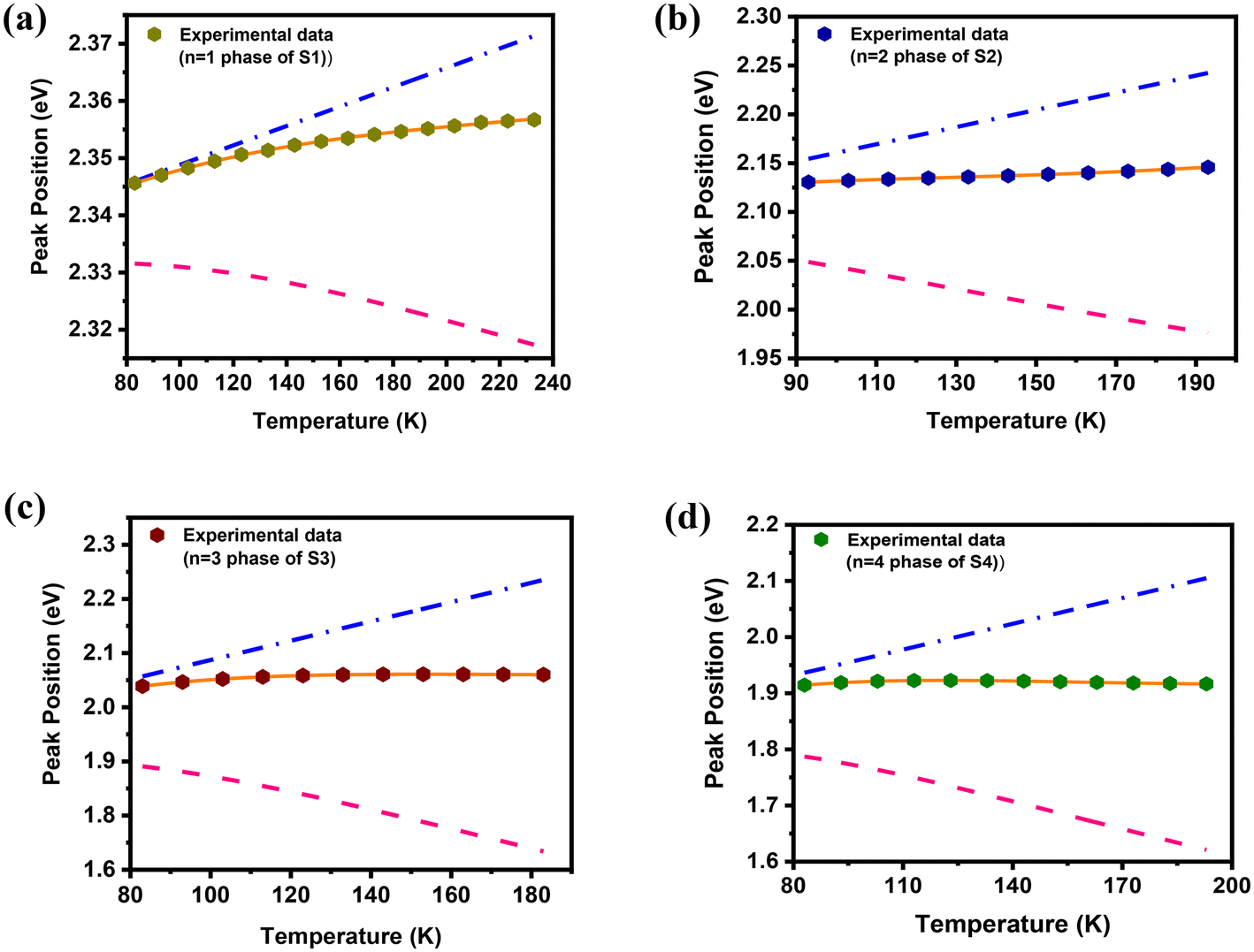 | ||
| Fig. 5 (a–d) Temperature-dependent PL peak positions of the main phases of samples S1–S4, respectively, fitted with eqn (3) (solid lines). The dashed-dotted (blue) and dashed (pink) lines show the individual contributions of thermal expansion and exciton–phonon interaction, respectively. | ||
| Sample | Phase | E 0 (eV) | A TE (meV K−1) | A EP (meV) | ħω (meV) |
|---|---|---|---|---|---|
| S1 | n = 1 | 2.332 ± 0.001 | 0.17 ± 0.01 | −58.46 ± 2.11 | 41.76 ± 2.38 |
| S2 | n = 2 | 2.073 ± 0.001 | 0.88 ± 0.03 | −176.94 ± 4.96 | 21.56 ± 1.05 |
| S3 | n = 3 | 1.85 ± 0.01 | 1.78 ± 0.21 | −578.17 ± 41.57 | 29.72 ± 1.10 |
| S4 | n = 4 | 1.80 ± 0.02 | 1.53 ± 0.25 | −476 ± 60 | 26.90 ± 0.83 |
Now to validate our results, we calculated the ratio between the free charge carriers and the excitons by using the Saha–Langmuir equation:60
 | (4) |
To obtain direct evidence of the increasing free carrier population in 2D perovskites with higher layer numbers, we measured the carrier mobility of mixed-phase perovskites. Metal–insulator–metal (MIM) sandwiched structures with the configuration aluminum (Al)/perovskite/indium tin oxide (ITO) were fabricated with a perovskite layer thickness of 200 nm. Current density–voltage (J–V) measurements for the fabricated devices were performed by applying voltage sweeps from −5 V to +5 V with a step size of 0.01 V (Fig. S7†). Under high electric fields, charge transport in the perovskite devices follows the space charge limited conduction (SCLC) mechanism.61 The current density in the SCLC regime can be described by the Mott–Gurney law:62
 | (5) |
Next, we performed time-resolved PL (TRPL) measurements of our mixed phase samples and the obtained decay curves are presented in Fig. 6 and Fig. S8.† To extract PL lifetimes, the decay traces can be analyzed with a multi-exponential function of the form
 | (6) |
 | (7) |
 is the fractional contribution of the ith decay component.
 | ||
| Fig. 6 Time-resolved PL for the main phases of samples S1–S4 with the fitting results (solid lines). The excitation wavelength was 400 nm. | ||
| Sample | Phase | τ 1 (ns) | f 1 (%) | τ 2 (ns) | f 2 (%) | τ avg (ns) |
|---|---|---|---|---|---|---|
| S1 | n = 1 | 0.19 | 100 | — | — | 0.19 |
| S2 | n = 2 | 0.23 | 99.36 | 3.54 | 0.64 | 0.25 |
| S3 | n = 3 | 0.53 | 94.26 | 4.31 | 5.73 | 0.75 |
| S4 | n = 4 | 0.64 | 87.25 | 3.43 | 12.75 | 0.99 |
| S4 | 3D | 2.38 | 65 | 44.7 | 35 | 17.19 |
As is evident from Table 2, the n = 1 phase exhibits no slow decay component, whereas the fractional contribution (f2) of the slow decay component increases progressively from n = 2 to the bulk phase. Moreover, the average PL lifetime (τavg) increases with increasing number of inorganic layers, reaching approximately 17 ns for the 3D phase of S4. These observations suggest that the incorporation of additional inorganic layers leads to a higher population of free carriers in the sample.
To quantify the exciton–phonon coupling strength, we analyzed the data showing the variation of PL linewidth with temperature. The PL linewidth in the presence of phonon scattering is described by the following equation:
 | (8) |
 , which means that the coupling strength decreases greatly as the temperature decreases.66 The last term is attributed to the inhomogeneous broadening from fully ionized impurities, where Eb and Γimp are the average binding energy of impurities and the coupling strength, respectively.66,67 According to the previous literature, scattering caused by impurities is not a significant factor in this case.57,68 Hence, we took the value of Γimp ≈ 0 for our analysis. The relevance of acoustic phonons with extremely low energy is notable only at low temperatures (below 100 K) and can be ignored in this case, as supported by various experimental investigations conducted on both 2D and 3D perovskites.68,69 Therefore, in our analysis, we considered only the broadening induced by lattice disorder (Γ0) and coupling with LO phonons (ΓLO). Fig. 7(a–d) show the evolution of FWHM with temperature for the main peaks of all the samples. The temperature variation of FWHM for other peaks of samples S2–S4 can be found in Fig. S9.†
 | ||
| Fig. 7 (a–d) Temperature-dependent full width at half maximum (FWHM) of the main PL peaks of the (TEA)2(MA)n−1PbnI3n+1, n = 1–4 films. The solid lines represent the fitting results using eqn (8). | ||
We previously mentioned that from the temperature-dependent shift of the PL peak position, a phase transition occurs at around 200 K for the 2D perovskites with n = 2, 3 and 4. Hence, we limited our fitting of the experimental data below the transition temperature. The fitting results for the main peaks of all the samples are presented in Fig. 7 and Table 3. The detailed analysis and the estimated values of ΓLO, γLO, and ELO corresponding to other peaks of samples S2–S4 are given in Table S4.†
| Sample | Phase | Γ 0 (meV) | γ LO (meV) | E LO (meV) |
|---|---|---|---|---|
| S1 | n = 1 | 10.9 ± 0.7 | 31 ± 4 | 13 ± 1 |
| S2 | n = 2 | 12.1 ± 0.4 | 33 ± 2 | 13.4 ± 0.2 |
| S3 | n = 3 | 25.6 ± 0.4 | 843 ± 33 | 67 ± 1 |
| S4 | n = 4 | 35.7 ± 0.9 | 695 ± 55 | 53 ± 1 |
It can be seen from Table 3 that both lattice disorder (Γ0) and scattering strength (γLO) are increased with an increase in the number of inorganic layers in the 2D perovskites. As the number of inorganic layers increases, the crystal structure becomes more complex, leading to increased disorder and defects within the material. These defects can act as scattering centers for phonons, causing them to scatter more frequently as they propagate through the material. With more layers, there are more interfaces where phonons can interact with each other. Nonetheless, adding more inorganic layers can introduce lattice mismatch between the layers causing strain. This strain can lead to phonon scattering as the lattice vibrations encounter changes in the local environment. It is evident from Table S4† that the values of the parameters Γ0, γLO, and ELO are different for the same perovskite phase of different samples. All these parameters are found to increase on going from film S2 to film S4. These 2D perovskite films were prepared by increasing the ratio of large organic and lead cations. As a result, all 2D phases (n = 1–4) are formed in S2–S4 with varying proportions. For example, S4 is expected to have more n = 4 phase than S2. Therefore, the surrounding environment of excitons in a particular phase undergoes notable transformations as one go from S1 to S4, which could be the possible reason for the enhanced values of the parameters. In essence, the incorporation of additional inorganic layers increases grain boundary scattering and consequently the overall strength of phonon scattering is enhanced within the material. Furthermore, we compared the values of the parameters AEP and γLO with those reported for 3D perovskites (Table 4). We found that both parameters for the n = 3 and n = 4 phases in our mixed-phase samples are higher than those of 3D perovskites. This strong carrier–phonon coupling in samples with higher layer numbers may be attributed to the presence of multiple coexisting phases.
4. Conclusions
In summary, we experimentally investigated how variations in the number of inorganic layers affect the optical and electronic properties of mixed-phase 2D-RP perovskites through temperature-dependent micro-PL measurements. As the layer number increases, both exciton–phonon interaction and thermal expansion significantly intensify, resulting in a reduction of the optical band gap at lower temperatures. The exciton/carrier–phonon interaction strength rises markedly from −58.46 meV for n = 1 to −476 meV for n = 4 driven by an increase in free charge carriers within the system. Similarly, the exciton–phonon scattering strength is substantially enhanced, increasing from 31 meV for n = 1 to 695 meV for n = 4, due to intensified lattice mismatch, greater interface complexity, and higher disorder within the system. Moreover, parameters associated with a particular 2D phase show considerable variability across different mixed-phase samples, likely due to structural distortion and changes in the surrounding environment caused by different amounts of large organic cations. These findings reveal the complex exciton–phonon coupling mechanisms within mixed-phase 2D-RP perovskites with varying layer numbers, highlighting their promising potential in future optoelectronic and spintronic device applications.Data availability
The data are available upon reasonable request from the corresponding author (suman@iitmandi.ac.in).Conflicts of interest
There are no conflicts to declare.Acknowledgements
The authors extend their gratitude to the Advanced Materials Research Centre (AMRC) at the Indian Institute of Technology Mandi for providing the necessary experimental facilities. S. S. acknowledges the Ministry of Education (MOE) for fellowship support. S. K. P. is grateful for the financial support from the Science and Engineering Research Board (SERB), Government of India (Grant No. CRG/2022/006320). We acknowledge the support of Dr Prakriti Ranjan Bangal's group at the CSIR-Indian Institute of Chemical Technology (CSIR-IICT) for their assistance with the TRPL measurements. We also appreciate the assistance of ChatGPT in editing the English text of this manuscript.References
- B. R. Sutherland and E. H. Sargent, Perovskite photonic sources, Nat. Photonics, 2016, 10(5), 295–302 CrossRef CAS.
- Z. Chen, Q. Dong, Y. Liu, C. Bao, Y. Fang, Y. Lin, S. Tang, Q. Wang, X. Xiao, Y. Bai, Y. Deng and J. Huang, Thin single crystal perovskite solar cells to harvest below-bandgap light absorption, Nat. Commun., 2017, 8(1), 1890 CrossRef PubMed.
- H. Huang, M. I. Bodnarchuk, S. V. Kershaw, M. V. Kovalenko and A. L. Rogach, Lead Halide Perovskite Nanocrystals in the Research Spotlight: Stability and Defect Tolerance, ACS Energy Lett., 2017, 2(9), 2071–2083 CrossRef CAS PubMed.
- E. Bi, H. Chen, F. Xie, Y. Wu, W. Chen, Y. Su, A. Islam, M. Grätzel, X. Yang and L. Han, Diffusion engineering of ions and charge carriers for stable efficient perovskite solar cells, Nat. Commun., 2017, 8(1), 15330 CrossRef CAS PubMed.
- C. M. Sutter-Fella, Y. Li, M. Amani, J. W. Ager, F. M. Toma III, E. Yablonovitch, I. D. Sharp and A. Javey, High Photoluminescence Quantum Yield in Band Gap Tunable Bromide Containing Mixed Halide Perovskites, Nano Lett., 2016, 16(1), 800–806 CrossRef CAS PubMed.
- M. Kundar, P. Kumar, S. K. Sharma, R. Singh and S. K. Pal, Stable Perovskite Solar Cells Based on Direct Surface Passivation Employing 2D Perovskites, Sol. RRL, 2023, 7(23), 2300572 CrossRef CAS.
- M. Yuan, L. N. Quan, R. Comin, G. Walters, R. Sabatini, O. Voznyy, S. Hoogland, Y. Zhao, E. M. Beauregard, P. Kanjanaboos, Z. Lu, D. H. Kim and E. H. Sargent, Perovskite energy funnels for efficient light-emitting diodes, Nat. Nanotechnol., 2016, 11(10), 872–877 CrossRef CAS PubMed.
- C. Qin, A. S. D. Sandanayaka, C. Zhao, T. Matsushima, D. Zhang, T. Fujihara and C. Adachi, Stable room-temperature continuous-wave lasing in quasi-2D perovskite films, Nature, 2020, 585(7823), 53–57 CrossRef CAS PubMed.
- W. Wu, X. Wang, X. Han, Z. Yang, G. Gao, Y. Zhang, J. Hu, Y. Tan, A. Pan and C. Pan, Flexible Photodetector Arrays Based on Patterned CH3NH3PbI3−xClx Perovskite Film for Real-Time Photosensing and Imaging, Adv. Mater., 2019, 31(3), 1805913 CrossRef PubMed.
- M. Kundar, K. Gayen, R. Ray, D. Kushavah and S. K. Pal, Highly stable two-dimensional Ruddlesden–Popper perovskite-based resistive switching memory devices, Nanoscale, 2024, 16(34), 16159–16171 RSC.
- M. A. Becker, R. Vaxenburg, G. Nedelcu, P. C. Sercel, A. Shabaev, M. J. Mehl, J. G. Michopoulos, S. G. Lambrakos, N. Bernstein, J. L. Lyons, T. Stöferle, R. F. Mahrt, M. V. Kovalenko, D. J. Norris, G. Rainò and A. L. Efros, Bright triplet excitons in caesium lead halide perovskites, Nature, 2018, 553(7687), 189–193 CrossRef CAS PubMed.
- M. Kim, J. Im, A. J. Freeman, J. Ihm and H. Jin, Switchable S = 1/2 and J = 1/2 Rashba bands in ferroelectric halide perovskites, Proc. Natl. Acad. Sci. U. S. A., 2014, 111(19), 6900–6904 CrossRef CAS PubMed.
- T. A. Berhe, W. N. Su, C. H. Chen, C. J. Pan, J. H. Cheng, H. M. Chen, M.-C. Tsai, L. Y. Chen, A. A. Dubale and B. J. Hwang, Organometal halide perovskite solar cells: degradation and stability, Energy Environ. Sci., 2016, 9(2), 323–356 RSC.
- S. Yang, Y. Wang, P. Liu, Y. B. Cheng, H. J. Zhao and H. G. Yang, Functionalization of perovskite thin films with moisture-tolerant molecules, Nat. Energy, 2016, 1(2), 15016 CrossRef CAS.
- L. N. Quan, M. Yuan, R. Comin, O. Voznyy, E. M. Beauregard, S. Hoogland, A. Buin, A. R. Kirmani, K. Zhao, A. Amassian, D. H. Kim and E. H. Sargent, Ligand-Stabilized Reduced-Dimensionality Perovskites, J. Am. Chem. Soc., 2016, 138(8), 2649–2655 CrossRef CAS PubMed.
- L. Mao, C. C. Stoumpos and M. G. Kanatzidis, Two-Dimensional Hybrid Halide Perovskites: Principles and Promises, J. Am. Chem. Soc., 2019, 141(3), 1171–1190 CrossRef CAS PubMed.
- C. C. Stoumpos, D. H. Cao, D. J. Clark, J. Young, J. M. Rondinelli, J. I. Jang, J. T. Hupp and M. G. Kanatzidis, Ruddlesden–Popper Hybrid Lead Iodide Perovskite 2D Homologous Semiconductors, Chem. Mater., 2016, 28(8), 2852–2867 CrossRef CAS.
- J. C. Blancon, A. V. Stier, H. Tsai, W. Nie, C. C. Stoumpos, B. Traoré, L. Pedesseau, M. Kepenekian, F. Katsutani, G. T. Noe, J. Kono, S. Tretiak, S. A. Crooker, C. Katan, M. G. Kanatzidis, J. J. Crochet, J. Even and A. D. Mohite, Scaling law for excitons in 2D perovskite quantum wells, Nat. Commun., 2018, 9(1), 2254 CrossRef PubMed.
- R. Su, C. Diederichs, J. Wang, T. C. H. Liew, J. Zhao, S. Liu, W. Xu, Z. Chen and Q. Xiong, Room-Temperature Polariton Lasing in All-Inorganic Perovskite Nanoplatelets, Nano Lett., 2017, 17(6), 3982–3988 CrossRef CAS PubMed.
- J. I. Fujisawa and T. Ishihara, Excitons and biexcitons bound to a positive ion in a bismuth-doped inorganic-organic layered lead iodide semiconductor, Phys. Rev. B:Condens. Matter Mater. Phys., 2004, 70(20), 205330 CrossRef.
- H. H. Fang, J. Yang, S. Adjokatse, E. Tekelenburg, M. E. Kamminga, H. Duim, J. Ye, G. R. Blake, J. Even and M. A. Loi, Band-Edge Exciton Fine Structure and Exciton Recombination Dynamics in Single Crystals of Layered Hybrid Perovskites, Adv. Funct. Mater., 2020, 30(6), 1907979 CrossRef CAS.
- S. Li, J. Luo, J. Liu and J. Tang, Self-Trapped Excitons in All-Inorganic Halide Perovskites: Fundamentals, Status, and Potential Applications, J. Phys. Chem. Lett., 2019, 10(8), 1999–2007 CrossRef CAS PubMed.
- G. Delport, G. Chehade, F. Lédée, H. Diab, C. Milesi-Brault, G. Trippé-Allard, J. Even, J.-S. Lauret, E. Deleporte and D. Garrot, Exciton–Exciton Annihilation in Two-Dimensional Halide Perovskites at Room Temperature, J. Phys. Chem. Lett., 2019, 10(17), 5153–5159 CrossRef CAS PubMed.
- M. Kepenekian, R. Robles, C. Katan, D. Sapori, L. Pedesseau and J. Even, Rashba and Dresselhaus Effects in Hybrid Organic–Inorganic Perovskites: From Basics to Devices, ACS Nano, 2015, 9(12), 11557–11567 CrossRef CAS PubMed.
- D. Giovanni, W. K. Chong, H. A. Dewi, K. Thirumal, I. Neogi, R. Ramesh, S. Mhaisalkar, N. Mathews and T. C. Sum, Tunable room-temperature spin-selective optical Stark effect in solution-processed layered halide perovskites, Sci. Adv., 2016, 2(6), e1600477 CrossRef PubMed.
- M. J. Crane, L. M. Jacoby, T. A. Cohen, Y. Huang, C. K. Luscombe and D. R. Gamelin, Coherent Spin Precession and Lifetime-Limited Spin Dephasing in CsPbBr3 Perovskite Nanocrystals, Nano Lett., 2020, 20(12), 8626–8633 CrossRef CAS PubMed.
- C. Wehrenfennig, G. E. Eperon, M. B. Johnston, H. J. Snaith and L. M. Herz, High Charge Carrier Mobilities and Lifetimes in Organolead Trihalide Perovskites, Adv. Mater., 2014, 26(10), 1584–1589 CrossRef CAS PubMed.
- M. S. Song, H. Wang, Z. F. Hu, Y. P. Zhang, T. Y. Liu and H. Y. Wang, The Role of Polaronic States on the Spin Dynamics in Solution-Processed Two-Dimensional Layered Perovskite with Different Layer Thickness, Adv. Sci., 2023, 10(26), 2302554 CrossRef CAS PubMed.
- M. Zhou, J. S. Sarmiento, C. Fei, X. Zhang and H. Wang, Effect of Composition on the Spin Relaxation of Lead Halide Perovskites, J. Phys. Chem. Lett., 2020, 11(4), 1502–1507 CrossRef CAS PubMed.
- M. Dyksik, S. Wang, W. Paritmongkol, D. K. Maude, W. A. Tisdale, M. Baranowski and P. Plochocka, Tuning the Excitonic Properties of the 2D (PEA)2(MA)n−1PbnI3n+1 Perovskite Family via Quantum Confinement, J. Phys. Chem. Lett., 2021, 12(6), 1638–1643 CrossRef CAS PubMed.
- C. M. Mauck, A. France-Lanord, A. C. Hernandez Oendra, N. S. Dahod, J. C. Grossman and W. A. Tisdale, Inorganic Cage Motion Dominates Excited-State Dynamics in 2D-Layered Perovskites (CxH2x+1NH3)2PbI4 (x = 4–9), J. Phys. Chem. C, 2019, 123(45), 27904–27916 CrossRef CAS.
- Z. Guo, X. Wu, T. Zhu, X. Zhu and L. Huang, Electron–Phonon Scattering in Atomically Thin 2D Perovskites, ACS Nano, 2016, 10(11), 9992–9998 CrossRef CAS PubMed.
- S. Wang, J. Ma, W. Li, J. Wang, H. Wang, H. Shen, J. Li, J. Wang, H. Luo and D. Li, Temperature-Dependent Band Gap in Two-Dimensional Perovskites: Thermal Expansion Interaction and Electron–Phonon Interaction, J. Phys. Chem. Lett., 2019, 10(10), 2546–2553 CrossRef CAS PubMed.
- J. Li, G. Lu, H. Xie, X. Jiang, Z. Fang, Y. J. Zeng, H. He and Z. Ye, Effect of Electron–Phonon Coupling on the Color Purity of Two-Dimensional Ruddlesden–Popper Hybrid Lead Iodide Perovskites, J. Phys. Chem. C, 2023, 127(13), 6380–6388 CrossRef CAS.
- A. A. Sutanto, N. Drigo, V. I. E. Queloz, I. Garcia-Benito, A. R. Kirmani, L. J. Richter, P. A. Schouwink, K. T. Cho, S. Paek, M. K. Nazeeruddin and G. Grancini, Dynamical evolution of the 2D/3D interface: a hidden driver behind perovskite solar cell instability, J. Mater. Chem. A, 2020, 8(5), 2343–2348 RSC.
- D. H. Cao, C. C. Stoumpos, O. K. Farha, J. T. Hupp and M. G. Kanatzidis, 2D Homologous Perovskites as Light-Absorbing Materials for Solar Cell Applications, J. Am. Chem. Soc., 2015, 137(24), 7843–7850 CrossRef CAS PubMed.
- B. H. Li, H. Di, H. Li, J. C. Wang, W. Zeng, D. B. Cheng, C. Zhou, X. Wang, Y. Shi, J. Song, Y. Zhao, X. Yang and Z. Ren, Unveiling the Intrinsic Photophysics in Quasi-Two-Dimensional Perovskites, J. Am. Chem. Soc., 2024, 146(10), 6974–6982 CrossRef CAS PubMed.
- K. Tanaka, T. Takahashi, T. Kondo, T. Umebayashi, K. Asai and K. Ema, Image charge effect on two-dimensional excitons in an inorganic-organic quantum-well crystal, Phys. Rev. B:Condens. Matter Mater. Phys., 2005, 71(4), 045312 CrossRef.
- T. Ogawa and Y. Kanemitsu, Optical Properties of Low-Dimensional Materials, 1995, vol. 1 Search PubMed.
- H. Long, X. Peng, J. Lu, K. Lin, L. Xie, B. Zhang, L. Ying and Z. Wei, Exciton–phonon interaction in quasi-two dimensional layered (PEA)2(CsPbBr3)n−1PbBr4 perovskite, Nanoscale, 2019, 11(45), 21867–21871 RSC.
- K. Wu, A. Bera, C. Ma, Y. Du, Y. Yang, L. Li and T. Wu, Temperature-dependent excitonic photoluminescence of hybrid organometal halide perovskite films, Phys. Chem. Chem. Phys., 2014, 16(41), 22476–22481 RSC.
- Z. Shao, S. You, X. Guo, J. Xiao, J. Liu, F. Song, H. Xie, J. Sun and H. Huang, Temperature-dependent photoluminescence of Co-evaporated MAPbI3 ultrathin films, Results Phys., 2022, 34, 105326 CrossRef.
- G. Plechinger, P. Nagler, J. Kraus, N. Paradiso, C. Strunk, C. Schüller and T. Korn, Identification of excitons, trions and biexcitons in single-layer WS2, Phys. Status Solidi RRL, 2015, 9(8), 457–461 CrossRef CAS.
- X. Wu, M. T. Trinh, D. Niesner, H. Zhu, Z. Norman, J. S. Owen, O. Yaffe, B. J. Kudisch and X. Y. Zhu, Trap States in Lead Iodide Perovskites, J. Am. Chem. Soc., 2015, 137(5), 2089–2096 CrossRef CAS PubMed.
- D. Li, G. Wang, H. C. Cheng, C. Y. Chen, H. Wu, Y. Liu, Y. Huang and X. Duan, Size-dependent phase transition in methylammonium lead iodide perovskite microplate crystals, Nat. Commun., 2016, 7(1), 11330 CrossRef CAS PubMed.
- J. Liu, J. Leng, K. Wu, J. Zhang and S. Jin, Observation of Internal Photoinduced Electron and Hole Separation in Hybrid Two-Dimentional Perovskite Films, J. Am. Chem. Soc., 2017, 139(4), 1432–1435 CrossRef CAS PubMed.
- B. Chon, J. Bang, J. Park, C. Jeong, J. H. Choi, J. B. Lee, T. Joo and S. Kim, Unique Temperature Dependence and Blinking Behavior of CdTe/CdSe (Core/Shell) Type-II Quantum Dots, J. Phys. Chem. C, 2011, 115(2), 436–442 CrossRef CAS.
- Z. Chen, C. Yu, K. Shum, J. J. Wang, W. Pfenninger, N. Vockic, J. Midgley and J. T. Kenney, Photoluminescence study of polycrystalline CsSnI3 thin films: Determination of exciton binding energy, J. Lumin., 2012, 132(2), 345–349 CrossRef CAS.
- D. G. Billing and A. Lemmerer, Synthesis, characterization and phase transitions in the inorganic-organic layered perovskite-type hybrids [(CnH2n + 1NH3)2PbI4], n = 4, 5 and 6, Acta Crystallogr., Sect. B, 2007, 63(5), 735–747 CrossRef CAS PubMed.
- K. P. O'Donnell and X. Chen, Temperature dependence of semiconductor band gaps, Appl. Phys. Lett., 1991, 58(25), 2924–2926 CrossRef.
- J. S. Manser, J. A. Christians and P. V. Kamat, Intriguing Optoelectronic Properties of Metal Halide Perovskites, Chem. Rev., 2016, 116(21), 12956–13008 CrossRef CAS PubMed.
- H. H. Fang, R. Raissa, M. Abdu-Aguye, S. Adjokatse, G. R. Blake, J. Even and M. A. Loi, Photophysics of Organic–Inorganic Hybrid Lead Iodide Perovskite Single Crystals, Adv. Funct. Mater., 2015, 25(16), 2378–2385 CrossRef CAS.
- J. Bhosale, A. K. Ramdas, A. Burger, A. Muñoz, A. H. Romero, M. Cardona, R. Lauck and R. K. Kremer, Temperature dependence of band gaps in semiconductors: Electron-phonon interaction, Phys. Rev. B:Condens. Matter Mater. Phys., 2012, 86(19), 195208 CrossRef.
- M. Cardona, Electron–phonon interaction in tetrahedral semiconductors, Solid State Commun., 2005, 133(1), 3–18 CrossRef CAS.
- C. Yu, Z. Chen, J. J. Wang, W. Pfenninger, N. Vockic, J. T. Kenney and K. Shum, Temperature dependence of the band gap of perovskite semiconductor compound CsSnI3, J. Appl. Phys., 2011, 110(6), 063526 CrossRef.
- K. Wei, Z. Xu, R. Chen, X. Zheng, X. Cheng and T. Jiang, Temperature-dependent excitonic photoluminescence excited by two-photon absorption in perovskite CsPbBr3 quantum dots, Opt. Lett., 2016, 41(16), 3821–3824 CrossRef CAS PubMed.
- L. Ni, U. Huynh, A. Cheminal, T. H. Thomas, R. Shivanna, T. F. Hinrichsen, S. Ahmad, A. Sadhanala and A. Rao, Real-Time Observation of Exciton–Phonon Coupling Dynamics in Self-Assembled Hybrid Perovskite Quantum Wells, ACS Nano, 2017, 11(11), 10834–10843 CrossRef CAS PubMed.
- Z. Chen, Y. Wang, X. Sun, Y. Guo, Y. Hu, E. Wertz, X. Wang, H. Gao, T. M. Lu and J. Shi, van der Waals Hybrid Perovskite of High Optical Quality by Chemical Vapor Deposition, Adv. Opt. Mater., 2017, 5(21), 1700373 CrossRef.
- X. Gong, O. Voznyy, A. Jain, W. Liu, R. Sabatini, Z. Piontkowski, G. Walters, G. Bappi, S. Nokhrin, O. Bushuyev, M. Yuan, R. Comin, D. McCamant, S. O. Kelley and E. H. Sargent, Electron–phonon interaction in efficient perovskite blue emitters, Nat. Mater., 2018, 17(6), 550–556 CrossRef CAS PubMed.
- M. N. Saha and A. Fowler, On a physical theory of stellar spectra, Proc. R. Soc. London, Ser. A, 1997, 99(697), 135–153 Search PubMed.
- K. Wang, C. Wu, D. Yang, Y. Jiang and S. Priya, Quasi-Two-Dimensional Halide Perovskite Single Crystal Photodetector, ACS Nano, 2018, 12(5), 4919–4929 CrossRef CAS PubMed.
- R. Ray, A. S. Sarkar and S. K. Pal, Improving carrier transport in polymer films by incorporating MoS2 nanosheets, J. Phys. D: Appl. Phys., 2020, 53(27), 275109 CrossRef CAS.
- Q. Han, S.-H. Bae, P. Sun, Y.-T. Hsieh, Y. Yang, Y. S. Rim, H. Zhao, Q. Chen, W. Shi, G. Li and Y. Yang, Single Crystal Formamidinium Lead Iodide (FAPbI3): Insight into the Structural, Optical, and Electrical Properties, Adv. Mater., 2016, 28(11), 2253–2258 CrossRef CAS PubMed.
- S. Rudin, T. L. Reinecke and B. Segall, Temperature-dependent exciton linewidths in semiconductors, Phys. Rev. B:Condens. Matter Mater. Phys., 1990, 42(17), 11218–11231 CrossRef CAS PubMed.
- A. K. Viswanath, J. I. Lee, D. Kim, C. R. Lee and J. Y. Leem, Exciton-phonon interactions, exciton binding energy, and their importance in the realization of room-temperature semiconductor lasers based on GaN, Phys. Rev. B:Condens. Matter Mater. Phys., 1998, 58(24), 16333–16339 CrossRef CAS.
- Y. Chen, G. P. Kothiyal, J. Singh and P. K. Bhattacharya, Absorption and photoluminescence studies of the temperature dependence of exciton life time in lattice-matched and strained quantum well systems, Superlattices Microstruct., 1987, 3(6), 657–664 CrossRef CAS.
- J. Lee, E. S. Koteles and M. O. Vassell, Luminescence linewidths of excitons in GaAs quantum wells below 150 K, Phys. Rev. B:Condens. Matter Mater. Phys., 1986, 33(8), 5512–5516 CrossRef CAS PubMed.
- A. D. Wright, C. Verdi, R. L. Milot, G. E. Eperon, M. A. Pérez-Osorio, H. J. Snaith, F. Giustino, M. B. Johnston and L. M. Herz, Electron–phonon coupling in hybrid lead halide perovskites, Nat. Commun., 2016, 7(1), 11755 CrossRef PubMed.
- T. Zhang, C. Zhou, X. Feng, N. Dong, H. Chen, X. Chen, L. Zhang, J. Lin and J. Wang, Regulation of the luminescence mechanism of two-dimensional tin halide perovskites, Nat. Commun., 2022, 13(1), 60 CrossRef CAS PubMed.
- H. C. Woo, J. W. Choi, J. Shin, S.-H. Chin, M. H. Ann and C.-L. Lee, Temperature-Dependent Photoluminescence of CH3NH3PbBr3 Perovskite Quantum Dots and Bulk Counterparts, J. Phys. Chem. Lett., 2018, 9(14), 4066–4074 CrossRef CAS PubMed.
- H.-H. Fang, F. Wang, S. Adjokatse, N. Zhao, J. Even and M. A. Loi, Photoexcitation dynamics in solution-processed formamidinium lead iodide perovskite thin films for solar cell applications, Light: Sci. Appl., 2016, 5(4), e16056–e16056 CrossRef CAS PubMed.
- S. Ghosh, Q. Shi, B. Pradhan, P. Kumar, Z. Wang, S. Acharya, S. K. Pal, T. Pullerits and K. J. Karki, Phonon Coupling with Excitons and Free Carriers in Formamidinium Lead Bromide Perovskite Nanocrystals, J. Phys. Chem. Lett., 2018, 9(15), 4245–4250 CrossRef CAS PubMed.
Footnote |
| † Electronic supplementary information (ESI) available. See DOI: https://doi.org/10.1039/d4nr04748f |
| This journal is © The Royal Society of Chemistry 2025 |