
 Open Access Article
 This Open Access Article is licensed under a Creative Commons Attribution-Non Commercial 3.0 Unported Licence
Small-signal capacitance in ferroelectric hafnium zirconium oxide: mechanisms and physical insights†
Revanth
Koduru
 *a,
Atanu K.
Saha
a,
Martin M.
Frank
b and
Sumeet K.
Gupta
a
*a,
Atanu K.
Saha
a,
Martin M.
Frank
b and
Sumeet K.
Gupta
a
aElmore Family School of Electrical and Computer Engineering, Purdue University, West Lafayette, IN 47907, USA. E-mail: kodurur@purdue.edu
bIBM Research, Yorktown Heights, NY 10598, USA
First published on 23rd January 2025
Abstract
This study presents a theoretical investigation of the physical mechanisms governing small-signal capacitance in ferroelectrics, focusing on hafnium zirconium oxide (Hf0.5Zr0.5O2, HZO). We utilize a time-dependent Ginzburg–Landau formalism-based 2D multi-grain phase-field framework to simulate the capacitance of metal–ferroelectric–insulator–metal (MFIM) capacitors. Our simulation methodology closely mirrors the experimental procedures for measuring ferroelectric small-signal capacitance, and the outcomes replicate the characteristic butterfly capacitance–voltage behavior. Notably, this behavior can be obtained without invoking traps. We delve into the components of the ferroelectric capacitance associated with the dielectric response and polarization switching, discussing the primary mechanisms – domain bulk response and domain wall response – contributing to the butterfly characteristics. We explore their interplay and relative contributions to the capacitance, correlating them to the polarization switching mechanisms and domain configurations. Additionally, we investigate the impact of increasing domain density with ferroelectric thickness scaling, demonstrating an enhancement in the polarization capacitance component, in addition to the dielectric component. Furthermore, we analyze the contributions of the domain bulk and domain wall responses across ferroelectric thicknesses, relating the capacitive memory window (for memory applications) to the capacitance and revealing a non-monotonic dependence of the maximum memory window on the ferroelectric thickness.
1 Introduction
Ferroelectric (FE) materials exhibit spontaneous polarization switched by external electric fields exceeding their coercive field. Historically, this hysteretic property has been of great interest for non-volatile memory applications.1 The recent discovery of ferroelectricity in doped hafnium oxide (HfO2)2 has revitalized interest in FE devices. The CMOS compatibility of HfO2 has led to the development of multiple flavors of FE devices for cutting-edge applications such as memory, computing in-memory (CiM), neuromorphic systems, and steep-slope transistors.3–7 The scale-free nature of ferroelectricity in HfO2,8 along with other appealing attributes,6,9–11 has positioned FE devices as promising contenders for future electronics.Another unique aspect of FE materials is their hysteretic, non-linear small-signal capacitance. This capacitive response, reflected in the butterfly capacitance–voltage (C–V) characteristics, has enabled applications in varactors, tunable filters, and oscillators.12–16 Recently, researchers have leveraged this FE capacitance property to propose non-destructive sensing for CiM applications.17–19 Given the broad range of applications for the capacitive behavior of ferroelectrics, a deep understanding of the underlying physical mechanisms assumes great importance for appropriate application-driven device optimization.
Historically, researchers have proposed several models to explain the butterfly C–V characteristics.16,20–32 Among these, the modified Johnson's model20 extends the original Johnson's model16 for paraelectrics to the FE state. This empirical approach shifts the electric field dependence of the dielectric permittivity to center around the coercive field of the FE material. While effective at reproducing the experimental butterfly C–V characteristics, its empirical nature limits the insights into the physical mechanisms governing the capacitance behavior.
Another class of approaches23–27 relates the FE C–V characteristics to the displacement of polarization domain walls (DWs). For instance, Placeres-Jiménez et al.25 extended Kittel26's approach of modeling DWs as rigid bodies moving under the action of an external electric field. In their work,25 the authors considered DWs as stretched membranes under external electric fields and studied their vibrational dynamics considering a linear restoration force. Employing this framework and incorporating the dependence of background permittivity on the electric field, the authors derived the equations for the butterfly C–V curves. However, these models are tailored for small changes in the applied electric field and often rely on the Preisach model or other phenomenological models to capture the large-signal hysteresis of ferroelectrics. As a result, these models are constrained in relating the capacitive behavior to polarization switching, and FE domain configurations.
Recent works by Massarotto et al.29,31 and Segatto et al.30 have addressed the long-standing gap between large-signal (LS) and small-signal (SS) capacitance characteristics of FE. Through experimental and simulation efforts, these studies have related the differences between LS and SS capacitance behavior to irreversible and reversible polarization switching.32 In their simulation works30,31 based on Landau–Ginzburg–Devonshire theory, the authors presented contrasting findings concerning the contribution of traps and FE response to the capacitance behavior. They further proposed that domain wall motion might not significantly contribute to the FE capacitance response. However, these conclusions are contingent upon the assumptions of fixed domains and the absence of inter-domain coupling utilized in their works.
Despite these advancements, a notable gap exists in understanding the physical mechanisms governing FE small-signal capacitance (SSC) characteristics, specifically correlating capacitance to FE polarization switching and domain configurations. The mechanisms driving the increase of capacitance well below the coercive voltage of ferroelectrics need to be explored. Furthermore, a self-consistent framework capturing the LS hysteresis and SS capacitance characteristics is yet to be developed. Such a framework would facilitate a more comprehensive understanding of the FE capacitance behavior and pave the way for extensive device optimizations.
To address these gaps, we present a multi-grain phase-field simulation framework based on the time-dependent Ginzburg Landau (TDGL) formalism for metal–ferroelectric–insulator–metal (MFIM) capacitors, as it is a basic structure in various FE devices. Our framework captures the large-signal charge (Q)–voltage (V) hysteresis and the small-signal butterfly C–V characteristics. The capacitance simulation methodology emulates the experimental process of FE small-signal capacitance (SSC) measurements and unravels the physical mechanisms governing the C–V response. Focusing on hafnium zirconium oxide (Hf0.5Zr0.5O2) or HZO as the FE material, we explore different components of the capacitive response in the MFIM stacks.
Our analysis unveils two distinct responses behind the butterfly C–V characteristics:
1. Domain bulk response: the response of regions within the bulk of FE domains.
2. Domain wall response: the response of regions in the domain walls of the FE layer, further comprising two sub-categories:
○ Wide domain wall response at the ferroelectric–dielectric (FE–DE) interface.
○ Domain wall vicinity response.
We delve into the physical aspects of these mechanisms and their contributions to the capacitance characteristics, exploring their dependence on the applied bias voltage and the FE polarization domain configurations. We further compare the mechanisms in the MFIM capacitors with the metal–ferroelectric–metal (MFM) capacitors, whose results are shown in ESI (S1 and S2†). Additionally, we investigate the impact of increasing domain density with ferroelectric thickness scaling on these different components, total FE capacitance, and the capacitive memory window for the CiM applications.
The key contributions of this work include:
• Presenting a self-consistent framework capturing both the large-signal and small-signal FE characteristics.
• Providing insights into the mechanisms governing the butterfly characteristics and the capacitance increase well below the coercive voltage of the FE.
• Correlating FE capacitance to the polarization switching mechanisms (domain growth and domain nucleation) and the domain configurations.
2 2D multi-grain phase-field simulation framework
We employ our in-house 2D multi-grain phase-field simulation framework (Fig. 1a), an extension of our previous works,33,34 to simulate the FE small-signal capacitance (SSC) of the MFIM stacks (Fig. 1c). This framework, based on the time-dependent Ginzburg Landau (TDGL) formalism and grain growth equation,35 captures the multi-domain P-switching in the FE layer while incorporating the polycrystalline nature of HZO. | ||
| Fig. 1 (a) 2D multi-grain phase-field simulation framework, illustrating the sequence of steps and equations involved, with arrows indicating the flow of variables across different stages. (b) Comparison of experimental charge (Q) versus applied voltage (Vapp) characteristics from Li et al.42 and simulated results (averaged over 20 samples) for MFIM stack with 10nm HZO ferroelectric layer and 2nm Al2O3 dielectric layer. (c) Reference MFIM structure. (d) List of calibrated parameters and their values for the 2D phase-field simulation framework. | ||
Polycrystallinity introduces spatial variations in material properties and polarization switching across the FE layer, resulting in the smooth and gradual polarization switching observed experimentally. Grain boundaries in polycrystalline structures act as pinning sites for domain walls, restricting their mobility36–38 and influencing the capacitance characteristics.25,26 These effects highlight the necessity of incorporating polycrystallinity into the analysis of SSC characteristics. By explicitly modeling polycrystallinity, we capture the effects of grain structure and boundaries on domain evolution and capacitance trends, addressing a gap in previous works20,25,29–31 that do not incorporate polycrystalline structure.
Furthermore, HZO exhibits an anisotropic crystal structure, with an alternate polar–spacer (APS) layer configuration along one cross-sectional direction and a fully polar (FP) configuration along the other.8,39 The low gradient energy (≈0) associated with the APS stabilizes unit-cell-wide domains, enabling elastically independent polarization switching along this direction.8,39 This leads to stripe-like polarization domains along the APS direction, as validated by first-principles simulations39 and recent experimental studies,40,41 particularly for the dimensions of Atomic Layer Deposited (ALD) HZO layer considered in this study.
Given these findings and the significant computational cost of the 3-dimensional (3D) phase-field simulations for the timescale of SSC measurements, we adopt 2-dimensional (2D) phase-field simulations. These 2D simulations focus on the fully polar (FP) and thickness directions of HZO and we believe these simulations reasonably approximate the MFIM capacitor's behavior.
It may be noted that a polycrystalline structure with different grain orientations could disrupt stripe-like domains across grains (Fig. S3a†). However, the 2D simulation methodology followed in this work represents a special case where the orientation of FP and APS layers align across the grains (Fig. S3b†). One can study this structure to understand the trends in capacitive behavior with the inter-grain variations incorporated in terms of Landau parameters.
The polycrystallinity of HZO is modeled by the grain growth equation (Fig. 1a.i),35 which captures the spatial and temporal evolution of the polycrystalline microstructure during crystallization, in terms of multiple abstract order parameters (ηk, 0 ≤ k ≤ K) as in eqn (1):
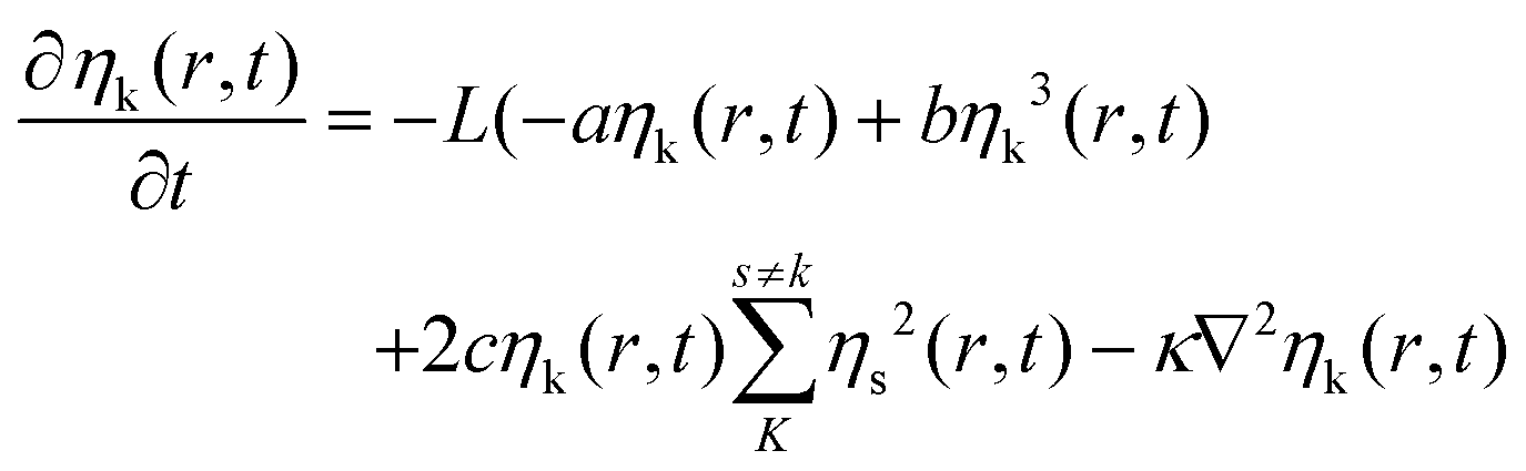
Here, r represents spatial coordinates and t represents time. The unitless parameters a = 1, b = 1, c = 1, L = 1, κ = 0.5, and K = 20 are calibrated to match the grain diameter distributions of simulated polycrystalline structures with experimental data43 for different HZO film thicknesses. Detailed calibration results are presented in our earlier work.44
The abstract parameters (ηk) represent variations across the grains in the polycrystalline structure, which can differ in properties, such as crystal orientation, material parameters, phase, and strain. In this work, we incorporate this inter-grain variability by considering spatial variations in the parameters of the TDGL equation, as discussed later.
To utilize the 3D polycrystalline structures generated by the grain growth equation in the 2D phase-field model, we extract the x–z slices (Fig. 1a.ii) of the 3D structure. The 3D structures, measuring 100 nm × 40 nm × 10 nm, are sliced along the y-axis, resulting in 2D x–z slices of 100 nm × 10 nm. Only the 2D slices with unique grain configuration are considered for FE HZO layer and each corresponds to one MFIM sample. In this study, we analyze the characteristics of 50 such unique MFIM samples.
The 2D phase-field framework (Fig. 1a.iv) models electrostatics and polarization (P) switching behavior of the MFIM stacks, accounting for the polycrystalline nature of the FE layer. The framework computes the potential ϕ and polarization P profiles by solving the time-dependent Ginzburg Landau (TDGL) and Poisson's equations. These equations are iteratively and self-consistently solved in 2D real space using a finite difference method with a grid spacing of 0.5 nm.33,44
The TDGL equation governs the dynamics of polarization switching in the FE layer, relating the rate of change in polarization (P) to the total energy of the system (F), given in its Euler–Lagrange form by eqn (2).
 | (2) |
The total energy (F), includes free energy (Ffree), electrostatic energy (Felec), and gradient energy (Fgrad) components in x- and z-directions; details of each of the energy components can be found in other work.33,45 Substituting these individual energy components in eqn (2) results in:
 | (3) |
Here, Γ is the viscosity coefficient, α, β, γ are the Landau free energy parameters, and g11, g33 are the gradient energy coefficients along the x- and z-directions, respectively.
To account for the inter-grain variability in the polycrystalline HZO layer, we introduce spatial variations in the Landau parameters (α, β, γ) across grains. For each grain (gi), the values αgi, βgi and γgi are sampled from Gaussian distributions centered around mean values (α0, β0 and γ0), with a standard deviation (σ0), as shown in Fig. 1a.iii. The mean values and standard deviation are calibrated based on experimental Q–V results.
Additionally, we account for the surface energy at the FE–DE interface via the extrapolation length formalism,46 resulting in the boundary condition given by:
 | (4) |
Poisson's equation (eqn (5)) describes the electrostatic behavior of the MFIM system in terms of the electrostatic potential (ϕ).
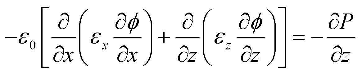 | (5) |
Here, ε0 represents the vacuum permittivity, εx and εz represent the relative material permittivity in the x- and z-directions, respectively. The right-hand side of eqn (5) accounts for the bound charges arising from the polarization gradients in the FE layer.
This framework captures polarization switching via domain growth and domain nucleation mechanisms in polycrystalline FE layers with non-uniform grain sizes and shapes. For simplicity, we focus on the orthorhombic phase of HZO and its ferroelectric behavior, despite the polymorphic nature of HZO, which includes monoclinic, orthorhombic and tetragonal phases.47 Extending the model to account for these multiple phases, and the Zr-doping dependent phase concentration,47,48 would require modifying the TDGL equation using Kittel's approach49 to capture both polar and anti-polar modes.48,50,51
In our simulations, we neglect leakage currents, which is reasonable given the thickness of the simulated MFIM stacks. We assume uniform strain and no inter-grain elastic interactions (g11 = 0 at the grain boundaries)52–54 as grain boundaries inhibit the continuation of domains unless specific symmetry conditions are satisfied.37,38 We consider trap/defect-free interfaces. Defects and traps at the interfaces or grain boundaries significantly impact polarization switching48 by inducing domain pinning,55,56 leading to asymmetric capacitance characteristics.28,57 Since our study primarily focuses on symmetric C–V butterfly curves, we disregard the influence of defects/traps. As we will demonstrate, the characteristic features of the symmetric small-signal C–V curves can be obtained without invoking traps.
We calibrate our framework using the experimental data from Li et al.42 for MFIM stacks with a 10 nm HZO FE layer and a 2 nm Al2O3 DE layer. To ensure robust calibration and account for polycrystallinity-induced device-to-device variations, we match the average Q–V characteristics of 20 simulated MFIM samples with experiments. The calibration of Landau parameters (α, β, γ) involves determining the mean values (α0, β0, γ0) and the standard deviation (σ0) of the Gaussian distribution from which individual grain parameters are sampled.
For Γ, we use a previously calibrated value of 0.6 S m−1.33 While this choice may affect the capacitance trends at high frequencies, we expect minimal impact on the capacitance and underlying physical mechanisms at the frequency of 1 MHz considered in this study. The final calibrated parameters of the 2D multi-grain phase-field simulation framework are summarized in Fig. 1d, alongside a comparison of simulated and experimental Q–V characteristics in Fig. 1b. Calibration and comparison of experimental and simulated characteristics for MFM stacks is shown in Fig. S1b and c.†
3 Ferroelectric small-signal capacitance: simulation methodology
Using the phase-field framework, we simulate the ferroelectric small-signal capacitance (SSC) by replicating experimental C–V measurement methodologies.31 To calculate the capacitance at a given DC bias voltage (V0), we simulate the MFIM stack under this bias V0 until it reaches a steady state (Fig. 2a). Steady state is defined as the condition where the normalized change polarization of the sample is less than 10−4%. Once a steady state is achieved, we superimpose a small-signal sinusoidal waveform (Vsin) with 1 MHz frequency and 1 mV amplitude onto the DC bias and simulate the response of the MFIM stack under this combined waveform (V0 + Vsin). | ||
| Fig. 2 (a) Voltage waveform for simulating capacitance–voltage (C–V) characteristics of the MFIM stack comprising a large-signal bias voltage (V0) superimposed with a small-signal sinusoidal waveform. (b) Q–V loop of MFIM stack showing the capacitor's charge response at different bias voltages (V01 and V02) in the insets. Small-signal charge response at a bias voltage of (c) V02, highlighting the initial irreversible response followed by reversible responses, and (d) V01, where only reversible response is observed. | ||
The charge response of the MFIM stack to V0 + Vsin consists of reversible and irreversible components,31,32 depending on the proximity of V0 to the sample's coercive voltage (±Vc).
• When V0 falls in non-switching regions of Q–V (e.g., V01 in Fig. 2b), far from ±VC, the small-signal charge response is purely reversible (Fig. 2d). This response arises primarily from the background permittivity of the materials and the oscillation of P-magnitude in the FE layer, without involving hysteretic P-switching.
• When V0 is in switching regions of the Q–V loop (e.g., V02 in Fig. 2b), near ±VC, the charge response involves both reversible and irreversible components. During initial cycles of Vsin, an irreversible component appears due to hysteretic P-switching (inset for V02 in Fig. 2b). However, after a few cycles, the irreversible switching diminishes, leaving only the reversible component (Fig. 2c).
We calculate the small-signal capacitance (C) solely from the reversible charge response as the ratio of the amplitude of the reversible charge (Qsin) to the applied sinusoidal voltage (Vsin) amplitude:
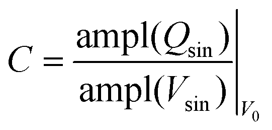 | (6) |
To generate the butterfly C–V curves (Fig. 3a), we vary V0 in steps of 50 mV, covering the forward (−5.5 V to 5.5 V) and backward (5.5 V to −5.5 V) paths. The capacitance at each voltage step is calculated using eqn (6) (Fig. 2a).
 | ||
| Fig. 3 (a) Simulated capacitance–voltage (C–V) characteristics for MFIM, averaged over 50 samples, with a 10 nm HZO FE layer and 2 nm Al2O3 dielectric layer. (b) Dielectric (CDE) and polarization (CP) capacitance components versus bias voltage, exhibiting inverted butterfly and butterfly characteristics respectively. (c) Schematic of MFIM structure, depicting multi-domain polarized FE layer with depolarization field and in-plane stray fields near domain walls at the FE–DE interface. Also shown are the average voltages on the top (VFE,top,avg) and bottom (VFE,bot,avg) interfaces of the FE layer used to calculate the average out-of-plane electric field (Ez,FE,avg). | ||
The small dimensions of the simulated MFIM samples (width of 100 nm) limit the number of grains in the FE layer. This results in sharp step transitions in the Q–V loops and multiple peaks and valleys in the C–V curves. To smooth these C–V characteristics, we average the C–V responses across 50 MFIM samples, each with a unique polycrystalline HZO layer. This approach also captures the effects of polycrystalline HZO on the C–V characteristics.
4 Ferroelectric small-signal capacitance: components
The simulation methodology used in this work is generic and applicable to a wide range of FE and DE thicknesses. However, since the phase-field framework has been calibrated for MFIM stacks with 10 nm HZO and 2 nm Al2O3, we focus on these specific thicknesses to investigate the mechanisms governing SSC characteristics over the next two sections. Additionally, we explore the capacitance trends for other FE thicknesses, such as 7 nm and 5 nm. For comparison, we also present the results for MFM stacks with 10 nm HZO in Fig. S1 and S2.† The simulated average C–V results of these MFIM stacks (Fig. 3a) as well as MFM (Fig. S1d†) successfully replicate the butterfly characteristics observed in experiments.31,41,42,47,58–60 To better understand the mechanisms governing these characteristics, we divide the total capacitance into dielectric and polarization capacitance components.Let us approach this division from the perspective of the total charge (Q) of the MFIM stack. It is evident that the HZO and Al2O3 (dead layers in MFM) layers, being in series, hold the same charge Q. In the HZO layer, Q embodies the combined effect of two phenomena: the background permittivity response, referred to as the dielectric component (Qde), and the response of the FE polarization domains to the electric field, or the polarization component (QP). These components sum up to produce the total dielectric response in the Al2O3 layer. Note, we can attribute a portion of Q in the Al2O3 layer (or the dead layers) as a response to the electric field/displacement of the FE dielectric component and the remaining portion as a response to the FE polarization component.
The dielectric (Qde) and polarization (QP) components of Q are calculated using the z-directed electric field (Ez,FE,avg) in the FE layer, averaged along the x-direction.61
| Qde = ε0εz,FEEz,FE,avg |
| QP = Q − Qde | (7) |
E z,FE,avg is determined from the average potential difference between the top interface of the FE layer (at Al2O3/HZO, VFE,top,avg) and the bottom interface (at HZO/metal, VFE,bot,avg) as in Fig. 3c.
 | (8) |
Here, TFE is the thickness of the FE layer.
Analogous to total charge (Q), the total capacitance (C) can be divided into dielectric (Cde) and polarization (CP) capacitance components. These are calculated using the corresponding sinusoidal responses of dielectric (Qde,sin) and polarization (QP,sin) charge components.
 | (9) |
 | (10) |
As shown in (Fig. 3b), Cde exhibits an inverted butterfly shape and CP displays the characteristic butterfly shape. CP is mainly responsible for the overall butterfly capacitance characteristics. Similar characteristics are observed for MFM stacks (Fig. S1e†). In the following subsections, we analyze these capacitance components in detail, highlighting the underlying physical mechanisms utilizing the spatial profiles of polarization P(x, z) and electric-field E(x, z) of a representative MFIM sample at different bias voltages (V0).
5 The dielectric capacitance component
The dielectric capacitance (Cde) arises from the background permittivity response of the MFIM stack to Vsin. This component (from eqn (9)) depends on the out-of-plane or z-directed electric field in MFIM and exhibits an inverted butterfly shape (Fig. 4a). | ||
| Fig. 4 (a) Dielectric capacitance (CDE) characteristics during the forward path, illustrating the inverted butterfly shape and the associated E-field transformations. Polarization and electric field profiles along the forward path at specific bias voltages of (b) V0 = −5.5 V, showing the smaller number of domains in the FE layer, with the inset highlighting lower in-plane E-field near DWs. (c) V0 = 1.8 V, with inset indicating an increase in the in-plane electric field component. (d) V0=4.7 V, displaying an increased number of domains and domain walls, leading to a stronger in-plane E-field, and (e) V0 = 5.5 V, showing the coalescence of +P domains, resulting in the reduction of the number of domain walls. | ||
To understand this behavior, let us discuss the formation of multi-domains in the FE layer (Fig. 3c) and its impact on E-field distribution. Imperfect screening of the polarization charges at the FE–DE interface generates a depolarization field—an electric field opposite to the P direction in the FE layer. This depolarization field increases the electrostatic energy (Felec) of the system, which ferroelectrics often minimize by breaking into multiple domains with opposite P directions (Fig. 3c), albeit at the cost of increased gradient energy.45 This multi-domain structure compensates the E-field lines originating from one domain in the adjacent oppositely polarized domains. This leads to in-plane E-fields or stray fields near domain walls (DW) at the FE–DE interface and reduces the out-of-plane E-field (Fig. 3c) and electrostatic energy.45
The strength of in-plane E-fields is proportional to the number of DWs in the FE layer. Moreover, this strength is maximized when the magnitudes of +P and −P domains across a DW are balanced.62 Variations in the relative magnitudes of these domains with changing bias voltage cause a redistribution of E-field between in-plane and out-of-plane directions. Since Cde depends on the out-of-plane E-field and the resulting induced charges on the metal electrodes, an increase in the in-plane E-field reduces Cde.
Let us discuss Cdeversus V0 focusing on the forward voltage path, where V0 increases from −5.5 V to 5.5 V (Fig. 4a). Starting at −5.5 V, the high negative bias stabilizes the majority of the FE layer in −P (blue regions in Fig. 4b), with fewer +P regions (red regions in Fig. 4b). This leads to fewer DWs and asymmetry in the domain magnitudes, with the magnitude of −P greater than +P domains. Consequently, most of the E-field is in the out-of-plane direction, with minimal in-plane components (inset of Fig. 4b), resulting in large Cde.
As V0 gradually increases, the magnitude of +P domains increases while that of −P domains decreases. This reduces the asymmetry between + P and −P domains (Fig. 4c) and allows for greater E-field compensation near the DWs. In other words, some out-of-plane E-field transforms to in-plane E-field (op-to-ip transformation), lowering Cde with increasing V0 (Fig. 4a). Due to the absence of multi-domain structure in MFM (Fig. S2a†) at high negative voltages, Cde does not show a significant decrease in MFM stacks until domain nucleation.
As V0 increases further and approaches coercive voltage (+VC), the FE layer undergoes P-switching through domain growth and domain nucleation (Fig. 4d). The nucleation of new +P domains increases the number of domains and DWs in the FE layer, enhancing the in-plane E-field at the FE–DE interface, leading to a continued decrease in Cde (Fig. 4a). Note that, the grain boundaries restrict the domain growth (Fig. 4d), inhibiting the propagation or continuation of domains across them, thereby pinning the domain wall at the grain boundaries. This occurs unless specific conditions related to crystallographic symmetry, the relative orientation of the two grains, and the orientation of grain boundary plane are satisfied.36–38
As V0 increases beyond +VC, the −P domains thin and collapse, coalescing +P domains (Fig. 4e). This reduces the number of DWs in the FE layer, decreases the in-plane E-field and increases the out-of-plane E-field (ip-to-op transformation). This change in the E-field distribution in the MFIM increases Cde with V0 for V0 > +VC (Fig. 4a).
Similar mechanisms, but in the opposite direction, govern Cde along the backward voltage path. As V0 decreases from 5.5 V, the reduced asymmetry between + P and −P domains increases the in-plane E-field, decreasing Cde. As V0 decreases further and approaches −VC, the nucleation of −P domains boosts the in-plane E-field, further reducing Cde. Finally, as V0 falls below −VC, the coalescence of −P domains reduces the in-plane E-field and increases the out-of-plane E-field and Cde. This interplay between in-plane and out-of-plane E-field transformations, P-switching via domain nucleation and coalescence, and the evolution of P-domain configurations results in the inverted butterfly characteristics of the dielectric capacitance component shown in Fig. 4a.
6 The polarization capacitance component
The polarization capacitance (CP) arises from the response of FE polarization domains to the sinusoidal waveform and exhibits butterfly shape (Fig. 3b). Our analysis reveals two physical responses governing CP characteristics across V0:1. Domain bulk response: This refers to the response of the FE regions deep within the polarization domains, away from the domain walls (DWs).
2. Domain wall response, which comprises:
○ Wide domain wall response: The response of wide domain walls or the “softer” domains near the FE–DE interface.
○ Domain wall vicinity response: This refers to the response of the FE regions adjacent to DWs.
Given the small amplitude of the sinusoidal voltage (1 mV), it is difficult to discern the small signal response directly in the polarization profiles of the FE layer. To illustrate these small changes in P, we utilize the polarization-amplitude (ampl-P) profiles (Fig. 5b) that depict the minute polarization response to Vsin. For any bias voltage, the polarization-amplitude profiles are obtained by spatially subtracting the polarization at the time when Vsin is zero (t0) from the polarization at the peak of the Vsin (tmax), as in Fig. 5a and eqn (11).
| ampl-P(x, z) = P(x, z, tmax) − P(x, z, t0) | (11) |
 | ||
| Fig. 5 (a) Method for calculating polarization–amplitude profile of the FE layer at any given bias voltage (V0), obtained by subtracting the polarization profile at the zero-crossing of the sinusoidal waveform (t0) from the polarization profile at sinusoidal peak (tmax). (b) Polarization–amplitude profile for V0 = 1.8 V. (c) Division of FE layer into domain wall and domain bulk regions for V0 = 1.8 V and (d) Polarization capacitance (CP) along with the domain bulk (CDB) and domain wall (CDW) capacitances versus bias voltage. | ||
To quantify the contributions of the domain bulk and domain wall responses, we define averaged domain bulk capacitance (CDB) and averaged domain wall capacitance (CDW), capturing the respective responses. Since these responses are spatially distributed, we partition the FE layer into domain bulk (DB) and domain wall (DW) regions based on P-magnitude and gradient energy. DW regions are characterized by lower P-magnitude and higher gradient energy than the DB regions. In the considered MFIM configuration, we typically observe hard or sharp DWs45 with no lattice points in the P transition region. For calculating CDW, lattice points on either side of the P-transition are included into the DW region, resulting in a DW width of 2 lattice points for hard DWs. Under certain conditions (discussed in section 6.2.1), softer DWs with widths greater than 2 lattice points are observed.
The averaged capacitances (CDB and CDW) are calculated at each V0 by spatially aggregating the ampl-P of the DB and DW regions. This aggregated value is then normalized with the sinusoidal voltage amplitude (ampl(Vsin) = 1 mV) and the area of the FE layer in x–z plane (Area = 100 nm × 10 nm), as follows:
 | (12) |
 | (13) |
Here, ampl-PDB(x, z) and ampl-PDW(x, z) represent the polarization-amplitude of the domain bulk and domain wall regions, respectively.
6.1 Domain bulk (DB) response
Domain bulk regions, characterized by low gradient energy, comprise both +P and −P domains. The minimal gradient energy implies that the polarization of DB regions is governed by the Landau–Khalatnikov (LK) equation, which accounts for Ffree and Felec contributions of the FE material (eqn (14))| E = αP + βP3 + γP5 | (14) |
The LK equation exhibits an S-shaped curve with segments of varying slopes—low, moderate, and high (marked in Fig. 6c)—that influence the response of DB regions to Vsin based on their location on the curve.
 | ||
| Fig. 6 (a) Polarization profile P(x, z) at V0 = −5.5 V, with reference points (in green stars) for analysis of P–E positions. (b) Polarization–amplitude profile ampl-P(x, z) at V0 = −5.5 V, showing the low response of domain bulk regions and the domain wall regions represented in black. (c) P–E positions of DB reference points plotted on the LK curve for V0 = −5.5 V and 1.8 V, showing traversal of +P domains along low-slope and −P domains towards high-slope segments. (d) Polarization and (e) polarization–amplitude profiles at V0 = 1.8 V, indicating the increase in the sinusoidal response of the DB regions. ampl-P(x, z) at (f) V0 = 4.7 V, showing a reduction in DB area due to domain nucleation, and (g) V0 = 5.5 V showing increased DB area due to domain coalescence. (h) P–E positions of DB reference points for V0 = 4.7 V, indicating the shift from the high-slope to the low-slope segment of the LK curve due to domain nucleation, with P(x, z) in the inset. (i) P–E positions of DB reference points for V0 = 5.5 V, indicating the shift along the low-slope segment of the LK curve, with P(x, z) in the inset. | ||
To illustrate this dependence, we select reference points in the DB regions of the FE layer (green stars in Fig. 6a) and examine their polarization (P) versus the experienced E-field calculated from the phase-field model. We refer to this as the P–E positions of these points and plot them against the S-shaped LK curve (Fig. 6c). Note that the LK curve is constructed using the mean Landau parameters (α0, β0, γ0), while the actual P–E positions account for the polycrystalline-induced variability (αgi, βgi, γgi) in the Landau parameters. The slope of the LK curve at each P–E position determines the response of these DB regions to Vsin.
Starting with the forward voltage path at V0 = −5.5 V, the FE layer is dominated by −P regions with thin +P domains (Fig. 6a). The P–E positions of the reference DB points (Fig. 6c, −5.5 V) fall in the low-slope segments of the LK curve. This indicates a minimal response of these DB regions to the Vsin, evident from the small ampl-P, approximately 10–4 μC cm−2 (Fig. 6b). Despite this low response, the large extent of DB regions across the FE layer means their collective contribution to the CP remains significant (Fig. 5d) (similarly in MFM Fig. S1f†).
As V0 increases but remains below +VC, P-switching is mainly driven by domain growth (Fig. 6d for 1.8 V). The polarization of +P domains increases, shifting their P–E positions further into the low-slope segment of the LK curve (Fig. 6c), which diminishes their response to Vsin. On the other hand, the magnitude of −P domains decreases, shifting their P–E positions towards the high-slope segment or the turnaround point of the LK curve (Fig. 6c). This increases their response to Vsin to approximately 10−3 μC cm−2 (Fig. 6e). Overall, CDB increases with V0 (Fig. 5d) as FE is predominantly negative polarized.
C DB increases with further increase in V0 as the P–E positions of −P domains move further towards the high-slope segment of the LK curve. As V0 approaches +VC, the P–E positions of −P domains reach the turnaround point of the LK curve, where even a slight increase in V0 switches from −P to +P polarization. The switching behavior, however, depends on the proximity of these −P regions to DWs. Regions near DWs switch via domain growth and their capacitive response is discussed in section 6.2.2 (on domain wall vicinity response). The regions away from DWs switch via domain nucleation, where new +P domains nucleate from the FE–DE interface.
The nucleation of +P domains relocates their P–E positions to the low-slope segment of the LK curve (Fig. 6h), reducing their response to the sinusoidal waveform. Additionally, nucleation increases the number of domains and DWs in the FE layer, reducing the DB regions (Fig. 6f). Thus, after nucleation, these two factors lead to a drop in CDB, which was previously increasing with V0. However, due to averaging over 50 MFIM samples with polycrystalline-induced variations in VC, we observe a relatively smooth decrease in CDB with V0.
With further increase in V0, the +P domains grow and coalesce, reducing the DW area and increasing the DB regions (Fig. 6g). However, the P–E positions of DB regions now traverse along a low-slope segment of the LK curve (Fig. 6i). This results in only a slight increase in CDB at high bias voltages (around 5 V in Fig. 5d).
Similar mechanisms involving the opposite polarization govern the domain bulk capacitance in the backward path. As V0 decreases from +5.5 V, +P DB regions move towards the high-slope segment of the LK curve, increasing CDB. Subsequently, +P domains switch to −P via domain nucleation reducing the DB regions, and CDB decreases. Following this, −P domains coalesce, slightly increasing CDB. These interactions—traversal along the LK curve by DB regions, polarization switching via domain nucleation and coalescence—govern the dependence of domain bulk capacitance (CDB) on bias voltage (Fig. 5d).
6.2 Domain wall response
Domain walls (DWs) refer to the transition regions between different polarization directions, in this case, +P and −P domains. These DW regions are characterized by high gradient energies due to spatial variations in polarization and a lower (closer to zero) P-magnitude compared with DB regions. Our analysis identifies two different DW responses to the sinusoidal waveform: wide DW response at the FE–DE interface and DW vicinity response.In the simulated MFIM structures, DWs are typically sharp or “hard” with a considered width of 2 lattice points. The response of hard DWs to Vsin is discussed in section 6.2.2 on domain wall vicinity response. However, for certain V0, we observe the formation of wide or “softer” DWs near the FE–DE interface. The width of these DWs is greater than 2 lattice points and we refer to the response of these regions as a wide domain wall response at the FE–DE interface, which we discuss next.
Wide DWs at the interface imply a slower transition of polarization to the domain bulk (DB) values compared with the regions away from the interface (FE bulk), as in Fig. 7c. In the FE bulk, DWs are sharp (hard), with P-magnitude on either side of DW close to DB values. However, at the interface, stray or in-plane E-fields near the DWs (discussed in section 5, Fig. 3c) reduce the out-of-plane E-field. This reduction lowers the polarization magnitudes, creating an additional transition zone between the +P and −P domains and thereby widening the DWs. This phenomenon is observable at any bias voltage (V0) and has been investigated in prior works63 and observed in other phase-field simulation works.61,64
 | ||
| Fig. 7 (a) Polarization profile at V0 = 0.3 V with black lines indicating grain boundaries. (b) Line plot of polarization along the thickness (z-direction) in +P and −P domains, illustrating the reduced polarization magnitude at the FE–DE interface compared with away from the interface and the polarization gradient along the z-direction. (c) Line plot of polarization along the x-direction crossing a domain wall, showing the widening of DW at the FE–DE interface compared with the FE bulk. (d) Polarization profile at V0 = −5.5 V highlighting the formation of conical domains at the interface near the grain boundaries and the reference points of plotted P–E positions in green stars. (e) Polarization–amplitude profile for V0 = −5.5 V, with a higher response at the wide DWs near the interface. (f) Reference points of +P domain (squares) and wide DW region (circles) plotted against the LK curve for V0 increasing from −5.5 V to −4 V, showing the traversal of wide DW point along the moderate-slope to high-slope segment and the +P domain point moving away from the high-slope segment. | ||
At high negative (positive) bias voltages, DW widening is more pronounced due to thin +P (−P) domains and strong depolarization fields. For instance, at V0 = −5.5 V, the thinning of +P domains (Fig. 7d) reduces the +P magnitude,62 even in regions away from the FE–DE interface. At the interface, this reduction of +P magnitude is intensified by the polarization gradient along z-direction (Fig. 7b), induced by the depolarization fields. The lower +P domain magnitude at the interface slows the transition between the +P and −P domains, further widening the DWs. As a result, we observe conical +P(−P) domains (Fig. 7d), with DWs near the interface exhibiting “softer” characteristics than those in the FE bulk.
These conical domains form head-to-head or tail-to-tail domain walls near the interface. These domain walls are experimentally observed in HZO40 and are shown to be stable under certain charge compensation conditions.65 In our simulations, conical domains are observed near the grain boundaries in the polycrystalline FE (Fig. 7d), where their stability is strongly influenced by the grain boundary effects. These conical +P (−P) domains minimize the energy of the system by compensating the depolarization field from the neighboring –P (+P) domains. This compensation occurs at the cost of gradient energy at only a single domain wall, consistent with our assumption of no inter-grain elastic interactions (g11 = 0 at the grain boundaries). Note that, such conical domains are absent in MFM structures due to the lower depolarization field (Fig. S2a and d†). Therefore, the capacitance in the MFM stack does not have a contribution from the wide domain wall response (Fig. S1f†).
To understand the wide DW response, we focus on the forward voltage path and the P–E positions of two reference lattice points (green stars in Fig. 7d): one located in the wide DW region and the other in the +P domain near the interface. At V0 = −5.5 V, the polarization in wide DW regions transitions gradually between oppositely polarized domains. As a result, their P–E positions lie along the moderate (negative)-slope segment of the LK curve (circle in Fig. 7f). The position on the negative slope of the LK curve is a localized and steady-state phenomenon that is consistent with the behavior of the softer DW regions reported in previous works.61,64 On the other hand, the P–E positions of +P domains near the interface fall along the high-slope segment (square in Fig. 7f), due to their slightly lower P-magnitude compared with FE bulk (away from the interface). Note that, these P–E positions deviate from the LK curve due to the high gradient energy associated with the DW and FE–DE interface regions.
The placement of P–E positions along the moderate and high-slope segments of the LK curve implies a heightened response to Vsin. This heightened response, as evident from the ampl-P profile (Fig. 7e), is approximately 10−2 μcm2 and is significantly higher than the response of DB regions (10−4 μcm2). However, since these regions constitute only a small portion of the FE layer, their aggregate response (CDW) is smaller than that of domain bulk (CDB) (Fig. 5d).
As V0 increases from −5.5 V, the polarization of +P domains increases, shifting their P–E positions towards the low-slope segment of the LK curve (squares in Fig. 7f). Simultaneously, the P–E positions of wide DW regions at the FE–DE interface traverse along the moderate slope segment towards the high-slope turnaround point (circles in Fig. 7f). However, due to the small area occupied by wide domain walls, domain wall capacitance (CDW) shows minimal variation with increasing the bias voltage (V0).
With the continued increase in V0, +P domains stabilize and the conical domains transform to more cylindrical shapes, reducing the width of DWs at the FE–DE interface. The previously “softer” (wide) domain walls transition to hard DWs, shifting their P–E positions to the low-slope segment of the LK curve (circle in Fig. 7f for V0 = −4 V). This reduces their response to the sinusoidal waveform, causing a slight dip in the domain wall capacitance (CDW), as highlighted in Fig. 5d. With a further increase in V0, the regions near the domain walls contribute to the overall response to the sinusoidal waveform, which will be discussed in the next section.
Similarly, at high positive bias voltages (V0 = 5.5 V), conical −P domains with wider domain walls at the FE–DE interface exhibit a higher response to the sinusoidal waveform. As V0 decreases, these conical −P domains transition to cylindrical domains, reducing DW widening and causing a dip in the domain wall capacitance (CDW). In summary, softer domains at the FE–DE interface with wider domain walls govern the wide-domain wall response at highly positive and negative bias voltages.
To understand these dependencies, we focus on the forward voltage path and examine the area surrounding a representative DW in the FE layer (dashed green line in Fig. 8a). The polarization in this region exhibits a sharp transition from +P to −P domains (black line in Fig. 8d). Let us consider the lattice points on either side of this region (green and purple markers in Fig. 8d) and examine their P–E positions over the range of V0 (2.3 to 2.35 V for the sample being discussed), where this DW undergoes motion or domain growth. Outside this range, the P–E positions of these points typically fall along the low-slope segment of the LK curve.
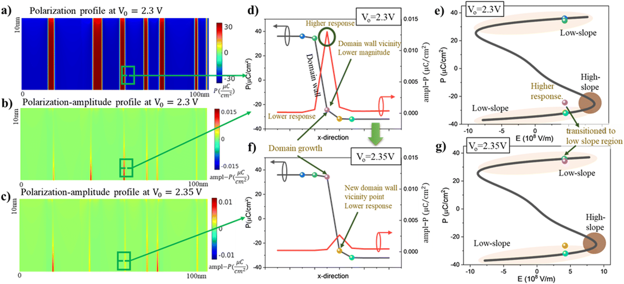 | ||
| Fig. 8 (a) Polarization profile and (b) polarization–amplitude profile for V0 = 2.3 V, showing the high response in the domain wall vicinity regions (green box). (c) Polarization–amplitude profile for V0 = 2.35 V, after domain growth, showing the reduced response in DW vicinity regions. (d) Line plot of polarization (black) and polarization–amplitude (red) along the x-direction near the highlighted DW region for V0 = 2.3 V, with the reference points (circles markers) to be plotted against the LK curve. (e) Reference points plotted against the LK curve for V0 = 2.3 V, showing the domain wall vicinity point in the high-slope region. (f) Line plot of polarization (black) and polarization–amplitude (red) for V0 = 2.35 V, illustrating the domain growth and the reduced polarization response. (g) Reference points against the LK curve for V0 = 2.35 V. | ||
At V0 = 2.3 V, the P–E position of +P lattice point (green marker) is along the low-slope segment of the LK curve (Fig. 8e), showing minimal response to Vsin (Fig. 8d). In contrast, the P–E position of −P lattice point (purple marker) is along the high-slope segment (Fig. 8e), exhibiting heightened response of around 1.5 × 10⁻² μC cm−2 (Fig. 8b, red line in Fig. 8d). This asymmetry in the polarization response between the two sides of the DW leads to a reversible shift in the DW position with the sinusoidal voltage, a phenomenon often referred to as “domain wall vibration” in the literature.23–26
A slight increase in V0 to 2.35 V causes the purple marker (exhibiting heightened response at 2.3 V) to switch to +P via domain growth or DW motion (Fig. 8f). This switching shifts its P–E position from the high-slope segment to the low-slope segment (purple marker in Fig. 8g), reducing its response to the sinusoidal waveform (purple marker in Fig. 8f). Meanwhile, the new −P lattice point (gold marker in Fig. 8f) adjacent to the transition region is still slightly away from the high-slope turnaround point (Fig. 8g). Due to the significant slope variation of the LK curve near the turnaround point, this gold lattice point exhibits a slightly lower sinusoidal response (Fig. 8f), around 2 × 10⁻³ μC cm−2. Consequently, the small-signal charge response near this DW diminishes at 2.35 V (Fig. 8c and f).
However, numerous DWs are present across the 50 different MFIM samples, with the polycrystalline variations introducing variability in the voltages at which these different DWs respond. Due to the Gaussian distribution of Landau parameters, we observe a Gaussian distribution for the voltages at which different DWs undergo DW motion. Consequently, as V0 increases, more DWs approach the threshold of the DW motion, continuously increasing CDW with V0 (Fig. 5d).
As V0 approaches the vicinity of coercive voltage (+Vc), the FE layer undergoes P-switching via domain nucleation (Fig. 4d). This process increases the number of +P domains and DWs in the FE layer (Fig. 6f), increasing the domain wall vicinity response. This is evident from the rise of CDW after the peak of domain bulk capacitance (which occurs before nucleation) in Fig. 5d. With further increase in V0, +P domains grow and coalesce (Fig. 4e), reducing the number of DWs in FE. As a result, CDW reaches a maximum and starts decreasing with increasing V0 above +VC (Fig. 5d).
Similar mechanisms but with opposite polarization govern CDW along the backward path. As V0 decreases from 5.5 V to −5.5 V, −P domains stabilize, enhancing the sinusoidal response of the +P regions near the DWs about to undergo domain growth. As V0 decreases further, more DWs approach the verge of DW motion, increasing CDW. With a further decrease in V0, −P domains nucleate, increasing the number of DWs and CDW. Eventually, CDW reaches a peak and decreases due to the coalescence of −P domains. These interactions between P-switching via domain growth, and the change in the number of DWs via domain nucleation and coalescence governs the domain wall vicinity response.
7 Ferroelectric small-signal capacitance: summary
Let us summarize the mechanisms behind the butterfly C–V characteristics. The total ferroelectric capacitance (CTOT) consists of dielectric (CDE) and polarization (CP) capacitance components. CDE exhibits an inverted butterfly shape due to the transformation between in-plane and out-of-plane electric fields, which mildly counteracts the butterfly trend of CP. In turn, CP—the primary driver of the butterfly shape—consists of domain bulk (CDB) and domain wall (CDE) responses, which are influenced by the domain configurations and voltage-dependent polarization switching mechanisms in the FE layer.Starting from V0 of −5.5 V and moving along the forward path, CTOT increases due to the dominance of CDB, as the −P DB regions shift from low-slope towards high-slope segment of the LK curve. Additionally, wide domain walls at the FE–DE interface due to the formation of conical +P domains at the grain boundaries contribute to the capacitance response in MFIM stacks. However, this effect diminishes as +P domains stabilize into cylindrical shapes with increasing V0. As +P domains stabilize with increasing V0, the contribution from the DW vicinity response increases, particularly from domains ready for growth. For the simulated configuration of 10 nm HZO with 2 nm Al2O3, due to the lower area of DWs, the DW vicinity response is less pronounced compared with the DB response for V0 < +VC.
As V0 approaches +VC, the −P DB regions reach the high-slope turnaround point of the LK curve, resulting in a peak in CTOT near +VC. Further increase in V0 leads to P-switching via nucleation of +P domains, which increases the area of DWs and reduces domain bulk regions. This causes a decrease in CDB while CDW increases to a peak value. After certain V0, +P domains coalesce, reducing the number of domain walls and CDW. CDB remains low as −P DB regions traverse the low-slope regions of the LK curve, thereby reducing CTOT above +VC.
On the reverse path, similar mechanisms lead to an initial increase in the capacitance up to a peak, followed by a decrease. In summary, the voltage-dependent interplay between domain bulk and domain wall responses, alongside polarization switching via domain growth, nucleation, and coalescence give rise to the butterfly C–V characteristics observed in MFIM stacks. Fig. 9 summarizes these different capacitance components.
 | ||
| Fig. 9 Summary of different capacitance components and responses in the metal–ferroelectric–insulator–metal (MFIM) capacitors. | ||
8 Scaling ferroelectric thickness and capacitive memory window
This section examines the impact of scaling the ferroelectric thickness on the small-signal C–V characteristics. We simulate MFIM stacks with HZO thicknesses of 5, 7, and 10 nm, each paired with a 2 nm Al2O3 layer. To ensure consistency, the bias voltage range was chosen to maintain a constant electric field across the FE layer at the maximum voltage point for each thickness. Note, we utilize the material and TDGL parameters calibrated for the 10 nm HZO and 2 nm Al2O3 MFIM sample. However, in practical scenarios, these parameters may vary with FE thicknesses due to strain, processing conditions, and others. Therefore, this section focuses on trends in capacitance behavior with FE thickness scaling rather than absolute capacitance values.The C–V characteristics (Fig. 10a) exhibit a butterfly shape across different FE thicknesses, with the total capacitance increasing as FE thickness scales down.59,60 As discussed in Section 4, the total capacitance can be divided into the dielectric capacitance (CDE) component with an inverted butterfly shape and the polarization capacitance (CP) with butterfly characteristics (Fig. 10b and c). Both CDE and CP increase with reducing FE thickness and we observe an expanded range of capacitance across bias voltage. Although the overall increase in capacitance partly results from reduced device thickness, our analysis shows that the polarization domain configurations also play a crucial role in this trend.
 | ||
| Fig. 10 (a) Simulated capacitance versus voltage (C–V) characteristics of MFIM stack (averaged over 50 samples) across FE thickness of 5, 7, and 10 nm HZO and highlighting the offset voltage (Vos), Chigh and Clow used for capacitive memory window calculation. (b) Dielectric capacitance (CDE–V), (c) Polarization capacitance component (CP–V), (d) Domain bulk capacitance (CDB–V) and (e) Domain wall capacitance (CDW–V) of the MFIM stack across different FE thicknesses. (f) Memory window for different offset voltages (Vos) across FE thicknesses of 5, 7, and 10 nm. | ||
Scaling down FE thickness increases the polarization domain density in the FE layer (Fig. 11a, b and c) due to the interplay between gradient and electrostatic energy, as demonstrated by previous studies.44,62 Higher domain density increases the area of DWs and reduces the DB regions. As a result, CDB decreases with FE thickness scaling (Fig. 10d), while CDW increases (Fig. 10e). The increase in CDW is larger than the decrease in CDB since DW regions lie on the high-slope segment of the LK curve, while DB regions generally fall into low-slope segments except on the verge of domain nucleation. Consequently, CDW contributes significantly to CP at lower FE thicknesses, leading to an additional component of the increase in CP with FE thickness scaling.
 | ||
| Fig. 11 Polarization profiles at a bias voltage of 0 V corresponding to negative remanent polarization (−PR) state for FE thicknesses of (a) 10 nm, (b) 7 nm, and (c) 5 nm showing an increase in domain density with scaling the FE thickness. Polarization profiles at bias voltage equal to the coercive voltage of the sample (+VC) corresponding to zero polarization state for FE thicknesses of (d) 10 nm, (e) 7 nm, and (f) 5 nm highlighting the reduced dominance of domain nucleation with FE thickness scaling. | ||
As FE thickness decreases, the increased domain density shifts the P-switching mechanism from a combination of domain growth and domain nucleation (at higher FE thicknesses) to predominantly domain growth (at lower FE thicknesses) (Fig. 11).62 As a result, at lower FE thickness, with more domain walls positioned for domain growth at a given bias voltage, especially near coercive voltage, we observe higher maximum CDW and thus a larger range of CDW and CP.
Examining CDE trends across FE thickness, we observe that increased domain density with FE thickness scaling enhances in-plane E-field (and reduces out-of-place E-fields), which lowers the charge response of the ferroelectric. As a result, CDE shows a lower increase with FE thickness scaling than it would if polarization domain effects were absent, i.e., a lower increase than when the capacitance change is strictly due to thickness scaling as in a dielectric material.
Additionally, we observe an increased range of CDE across bias voltages for thinner FE layers (7 and 5 nm), which can be understood as follows. On the forward path, beginning from the most negative bias voltage, even with the increased domain density, most of the E-field is oriented out-of-plane due to the asymmetry in the magnitudes of +P and −P domains. As V0 increases, this asymmetry decreases, shifting the E-field from out-of-plane to in-plane direction. The higher domain density and, in turn, higher DW area in thinner FE layers promote this op-to-ip transformation more than at 10 nm. As a result, CDE reduces significantly with V0 increase for lower FE thicknesses, leading to a higher range of CDE as FE thickness scales down.
However, at lower FE thicknesses, we observe deviations in the C–V characteristics from the traditional butterfly curves59,60 (highlighted in Fig. 10a). First, there is an initial decrease in capacitance (highlighted in blue in Fig. 10a) as V0 moves from extreme negative (positive) bias voltage towards zero on the forward (backward) voltage paths. This decrease stems from the wide domain wall response at the FE–DE interface. At high negative V0, conical +P domains form near the FE–DE interface with the P–E position of +P domain point at the interface along the high-slope segment of the LK curve (refer to section 6.2.1). As V0 increases, these regions shift toward the low-slope segment, reducing its response to the sinusoidal waveform. This effect is more pronounced at lower FE thicknesses due to higher DW density, reducing CTOT as highlighted in blue in Fig. 10a. Some experimental characteristics presented show a capacitance increase at higher voltages30,31,58 for scaled FE thicknesses, which is often attributed to leakage currents.58 The prevalence of leakage currents at high voltages makes the identification and validation of the capacitance increase due to the wide DW response challenging.
Additionally, small bumps in the capacitance (highlighted in green in Fig. 10a) are observed as V0 transitions from most negative (positive) voltage to 0 V. This phenomenon is also due to the wide-DW response at the FE–DE interface. At high negative V0, the “softer” DW regions associated with the conical +P domains have their P–E positions along the moderate-slope segment of the LK curve (refer to section 6.2.1). As V0 increases, these P–E positions shift along the moderate-slope segment towards the high-slope segment, briefly enhancing their response to the sinusoidal waveform. With further increase in V0, these P–E positions eventually move to the low-slope segment, reducing CTOT. Due to the higher domain density at lower FE thicknesses, this effect creates the observed bumps in CTOT. This phenomenon needs further investigation with rigorous 3D simulations and experimental characterizations at scaled FE thickness and device dimensions.
We further explore the impact of increased domain density and FE thickness scaling on the capacitive memory window (MW), a crucial metric for capacitive compute-in-memory (CiM) applications.17–19 In capacitive CiM applications, FE capacitors are utilized by creating a capacitance difference between the forward and backward paths (or the low and high capacitance states) at zero bias voltage. This difference is achieved either by introducing a non-zero offset voltage (Vos) across the FE capacitor or by incorporating traps, leading to asymmetric butterfly C–V characteristics.18 For our analysis, we consider the former method of using offset voltage.
We vary the offset voltage (Fig. 10a) and examine the trends in the capacitive MW, defined as the ratio between the high (Chigh) and low (Clow) capacitance states17 (as marked in Fig. 10a). We observe a non-monotonic capacitive MW response to Vos across FE thicknesses (Fig. 10f): the capacitive MW initially increases with Vos and then decreases leading to a peak in the MW at certain Vos, due to the butterfly shape of the FE C–V characteristics.
Peak capacitive MW shows a non-monotonic dependence on FE thickness (Fig. 10f). As thickness scales from 10 to 7 nm, capacitive MW peaks increase, largely due to the expanded range of CTOT. However, scaling to 5 nm reduces the peak capacitive MW, despite the increased CTOT range. This reduction occurs because the Chigh peak at 5nm coincides with a bump in the Clow branch, reducing the peak Chigh/Clow ratio. As mentioned, this behavior and the bumps in the butterfly curves warrant further investigation.
Nevertheless, the dependence of capacitive MW on FE thickness highlights the important role played by P-domain configurations on the MFIM capacitance behavior. If the capacitance changes were solely due to geometry (thickness) scaling, the MW would remain constant across different FE thicknesses. However, the change in the capacitive MW with FE thickness underlines the importance of understanding the effects of polarization domain configurations and switching mechanisms to drive application-driven FE capacitance devices.
9 Conclusions
In summary, we have investigated the butterfly ferroelectric capacitance–voltage characteristics, emphasizing the contributions of the dielectric and polarization capacitance components and the physical mechanisms governing them. We have identified and examined three key mechanisms governing the polarization capacitance component. First, the domain bulk response, the response of the regions away from the domain walls, contributes significantly to the ferroelectric capacitance at higher FE thicknesses. Second, the wide domain wall response at the FE–DE interface is prevalent only at the extreme negative and positive bias voltages. Third, the domain wall vicinity response near the domain wall regions plays a crucial role as FE thickness scales down. We further discuss the impact of FE thickness scaling and the resultant increase in the domain density on the capacitance–voltage characteristics and the capacitive memory window, showing a non-monotonic trend in the peak capacitive memory window as a function of FE thickness.Author contributions
Conceptualization: R.K., A.K.S., M.M.F. and S.K.G.; data curation and formal Analysis: R.K. and S.K.G; funding acquisition: S.K.G.; investigation: R.K.; methodology: R.K., A.K.S., M.M.F. and S.K.G; project administration: S.K.G.; software: R.K., A.K.S. and S.K.G.; resources: A.K.S. and S.K.G; supervision: M.M.F. and S.K.G.; validation: M.M.F. and S.K.G.; visualization: R.K., M.M.F. and S.K.G.; writing – original draft: R.K., M.M.F. and S.K.G.; writing – review & editing: R.K., M.M.F. and S.K.G.Data availability
Data for this article are available in the following folder “small signal capacitance” at https://purdue0-my.sharepoint.com/:f:/g/personal/kodurur_purdue_edu/EvPvV56EY21Nstr7IlLM7K8BP_unzl6mRkkL8v4vbros3Q?e=cMuTnk.Conflicts of interest
There are no conflicts of interest to declare.Acknowledgements
This work was supported, in part, by the National Science Foundation under Grant No. 2008412, by the Semiconductor Research Corporation (SRC) Global Research Collaboration (GRC) program under LMD task 2959.001, and by the Center for the Co-Design of Cognitive Systems (COCOSYS), one of the seven centers in JUMP 2.0, an SRC program sponsored by DARPA.References
- J. F. Scott, Science, 2007, 315, 954–959 CrossRef CAS PubMed.
- T. S. Böscke, J. Müller, D. Bräuhaus, U. Schröder and U. Böttger, Appl. Phys. Lett., 2011, 99, 102903 CrossRef.
- M. Jerry, S. Dutta, A. Kazemi, K. Ni, J. Zhang, P.-Y. Chen, P. Sharma, S. Yu, X. S. Hu, M. Niemier and S. Datta, J. Phys. D: Appl. Phys., 2018, 51, 434001 CrossRef.
- K. Ni, B. Grisafe, W. Chakraborty, A. K. Saha, S. Dutta, M. Jerry, J. A. Smith, S. Gupta and S. Datta, 2018 IEEE International Electron Devices Meeting (IEDM), 2018, pp. 16.1.1–16.1.4.
- H. Mulaosmanovic, E. Chicca, M. Bertele, T. Mikolajick and S. Slesazeck, Nanoscale, 2018, 10, 21755–21763 RSC.
- E. Ko, H. Lee, Y. Goh, S. Jeon and C. Shin, IEEE J. Electron Devices Soc., 2017, 5, 306–309 CAS.
- U. Schroeder, M. H. Park, T. Mikolajick and C. S. Hwang, Nat. Rev. Mater., 2022, 7, 653–669 CrossRef.
- H.-J. Lee, M. Lee, K. Lee, J. Jo, H. Yang, Y. Kim, S. C. Chae, U. Waghmare and J. H. Lee, Science, 2020, 369, 1343–1347 CrossRef CAS PubMed.
- H. Mulaosmanovic, T. Mikolajick and S. Slesazeck, ACS Appl. Mater. Interfaces, 2018, 10, 23997–24002 CrossRef CAS PubMed.
- M. Hoffmann, M. Pešić, K. Chatterjee, A. I. Khan, S. Salahuddin, S. Slesazeck, U. Schroeder and T. Mikolajick, Adv. Funct. Mater., 2016, 26, 8643–8649 CrossRef CAS.
- A. K. Saha, K. Ni, S. Dutta, S. Datta and S. Gupta, Appl. Phys. Lett., 2019, 114, 202903 CrossRef.
- V. K. Varadan, K. A. Jose, V. V. Varadan, R. Hughes and J. F. Kelly, Microwave J., 1995, 38, 244–249 Search PubMed.
- D. Ghodgaonkar, R. Hughes, F. Selmi, V. Varadan and V. Varadan, IEEE Antennas and Propagation Society International Symposium 1992 Digest, 1992, vol. 1, pp. 272–275.
- Z. Wang and A. I. Khan, IEEE J. Explor. Solid-State Comput. Devices Circuits, 2019, 5, 151–157 Search PubMed.
- N. Thakuria, A. K. Saha, S. K. Thirumala, B. Jung and S. K. Gupta, IEEE Trans. Electron Devices, 2019, 66, 2415–2423 CAS.
- K. M. Johnson, J. Appl. Phys., 1962, 33, 2826–2831 CrossRef.
- S. Mukherjee, J. Bizindavyi, S. Clima, M. I. Popovici, X. Piao, K. Katcko, F. Catthoor, S. Yu, V. V. Afanas'ev and J. Van Houdt, IEEE Electron Device Lett., 2023, 44, 1092–1095 CAS.
- T.-H. Kim, O. Phadke, Y.-C. Luo, H. Mulaosmanovic, J. Mueller, S. Duenkel, S. Beyer, A. I. Khan, S. Datta and S. Yu, IEEE Electron Device Lett., 2023, 44, 1628–1631 Search PubMed.
- S. Yu, Y.-C. Luo, T.-H. Kim and O. Phadke, IEEE Electron Devices Mag., 2023, 1, 23–32 Search PubMed.
- M. Narayanan, S. Tong, B. Ma, S. Liu and U. Balachandran, Appl. Phys. Lett., 2012, 100, 022907 CrossRef.
- H. Li and G. Subramanyam, IEEE Trans. Ultrason. Ferroelectr. Freq. Control, 2009, 56, 1861–1867 Search PubMed.
- C. J. Brennan, Integr. Ferroelectr., 1992, 2, 73–82 CrossRef CAS.
- C. Ang and Z. Yu, Appl. Phys. Lett., 2004, 85, 3821–3823 CrossRef CAS.
- Q. M. Zhang, H. Wang, N. Kim and L. E. Cross, J. Appl. Phys., 1994, 75, 454–459 CrossRef CAS.
- R. Placeres-Jiménez, J. P. Rino, A. M. Gonçalves and J. A. Eiras, J. Phys. D: Appl. Phys., 2015, 48, 465301 CrossRef.
- C. Kittel, Phys. Rev., 1951, 83, 458–458 CrossRef CAS.
- L. Jin, V. Porokhonskyy and D. Damjanovic, Appl. Phys. Lett., 2010, 96, 242902 CrossRef.
- Y.-C. Luo, J. Hur, P. Wang, A. I. Khan and S. Yu, Appl. Phys. Lett., 2020, 117, 073501 CrossRef CAS.
- M. Massarotto, F. Driussi, A. Affanni, S. Lancaster, S. Slesazeck, T. Mikolajick and D. Esseni, Solid-State Electron., 2023, 200, 108569 CrossRef CAS.
- M. Segatto, M. Massarotto, S. Lancaster, Q. T. Duong, A. Affanni, R. Fontanini, F. Driussi, D. Lizzit, T. Mikolajick, S. Slesazeck and D. Esseni, ESSDERC 2022 – IEEE 52nd European Solid-State Device Research Conference (ESSDERC), 2022, pp. 340–343.
- M. Massarotto, M. Segatto, F. Driussi, A. Affanni, S. Lancaster, S. Slesazeck, T. Mikolajick and D. Esseni, 2023 35th International Conference on Microelectronic Test Structure (ICMTS), 2023, pp. 1–6.
- D. Bolten, U. Böttger and R. Waser, J. Eur. Ceram. Soc., 2004, 24, 725–732 CrossRef CAS.
- R. Koduru, I. Ahmed, A. K. Saha, X. Lyu, P. Ye and S. K. Gupta, J. Appl. Phys., 2023, 134, 084104 CrossRef CAS.
- A. K. Saha, M. Si, P. D. Ye and S. K. Gupta, Appl. Phys. Lett., 2021, 119, 122903 CrossRef CAS.
- C. E. Krill III and L. Q. Chen, Acta Mater., 2002, 50, 3059–3075 CrossRef.
- B. J. Rodriguez, Y. H. Chu, R. Ramesh and S. V. Kalinin, Appl. Phys. Lett., 2008, 93, 142901 CrossRef.
- S. Mantri, J. Oddershede, D. Damjanovic and J. E. Daniels, Acta Mater., 2017, 128, 400–405 CrossRef CAS.
- S. Mantri and J. E. Daniels, IEEE Trans. Ultrason. Ferroelectr. Freq. Control, 2018, 65, 1517–1524 Search PubMed.
- T. K. Paul, A. K. Saha and S. K. Gupta, Adv. Electron. Mater., 2024, 10, 2300400 CrossRef CAS.
- K. Park, D. Kim, K. Lee, H.-J. Lee, J. Kim, S. Kang, A. Lin, A. J. Pattison, W. Theis, C. H. Kim, H. Choi, J. W. Cho, P. Ercius, J. H. Lee, S. C. Chae and J. Park, ACS Nano, 2024, 18(38), 26315–26326 CAS.
- S. Zhang, Q. Zhang, F. Meng, T. Lin, B. Zeng, L. Gu, M. Liao and Y. Zhou, Research, 2023, 6, 0093 CrossRef CAS PubMed.
- J. Li, Y. Qu, M. Si, X. Lyu and P. D. Ye, 2020 IEEE Symposium on VLSI Technology, Honolulu, HI, USA, 2020, pp. 1–2.
- M. H. Park, Y. H. Lee, H. J. Kim, T. Schenk, W. Lee, K. D. Kim, F. P. G. Fengler, T. Mikolajick, U. Schroeder and C. S. Hwang, Nanoscale, 2017, 9, 9973–9986 RSC.
- R. Koduru, A. K. Saha, M. Si, X. Lyu, P. D. Ye and S. K. Gupta, 2021 IEEE International Electron Devices Meeting (IEDM), 2021, pp. 15.2.1–15.2.4.
- A. K. Saha and S. K. Gupta, Sci. Rep., 2020, 10, 10207 CrossRef CAS PubMed.
- L. Hong, A. K. Soh, Y. C. Song and L. C. Lim, Acta Mater., 2008, 56, 2966–2974 CrossRef CAS.
- J. Müller, T. S. Böscke, U. Schröder, S. Mueller, D. Bräuhaus, U. Böttger, L. Frey and T. Mikolajick, Nano Lett., 2012, 12, 4318–4323 CrossRef PubMed.
- S.-C. Chang, K. Chae, M. I. Popovici, C.-C. Lin, S. Siddiqui, I.-C. Tung, J. Bizindavyi, B. G. Alpizar, N. Haratipour, M. Metz, J. Kavalieros, G. S. Kar, A. Kummel, K. Cho and U. E. Avci, 2022 International Electron Devices Meeting (IEDM), 2022, pp. 13.1.1–13.1.4.
- C. Kittel, Phys. Rev., 1951, 82, 729–732 CrossRef CAS.
- A. N. Morozovska, M. V. Strikha, K. P. Kelley, S. V. Kalinin and E. A. Eliseev, Phys. Rev. Appl., 2023, 20, 054007 CrossRef CAS.
- T. R. Kim, A. K. Saha and S. K. Gupta, 2023 Device Research Conference (DRC), 2023, pp. 1–2.
- S. Deng, G. Yin, W. Chakraborty, S. Dutta, S. Datta, X. Li and K. Ni, 2020 IEEE Symposium on VLSI Technology, 2020, pp. 1–2.
- K. Ni, W. Chakraborty, J. Smith, B. Grisafe and S. Datta, 2019 Symposium on VLSI Technology, 2019, pp. T40–T41.
- J. P. B. Silva, R. Alcala, U. E. Avci, N. Barrett, L. Bégon-Lours, M. Borg, S. Byun, S.-C. Chang, S.-W. Cheong, D.-H. Choe, J. Coignus, V. Deshpande, A. Dimoulas, C. Dubourdieu, I. Fina, H. Funakubo, L. Grenouillet, A. Gruverman, J. Heo, M. Hoffmann, H. A. Hsain, F.-T. Huang, C. S. Hwang, J. Íñguez, J. L. Jones, I. V. Karpov, A. Kersch, T. Kwon, S. Lancaster, M. Lederer, Y. Lee, P. D. Lomenzo, L. W. Martin, S. Martin, S. Migita, T. Mikolajick, B. Noheda, M. H. Park, K. M. Rabe, S. Salahuddin, F. Sánchez, K. Seidel, T. Shimizu, T. Shiraishi, S. Slesazeck, A. Toriumi, H. Uchida, B. Vilquin, X. Xu, K. H. Ye and U. Schroeder, APL Mater., 2023, 11, 089201 CrossRef CAS.
- M. Pešić, F. P. G. Fengler, L. Larcher, A. Padovani, T. Schenk, E. D. Grimley, X. Sang, J. M. LeBeau, S. Slesazeck, U. Schroeder and T. Mikolajick, Adv. Funct. Mater., 2016, 26, 4601–4612 CrossRef.
- W. Yang, J. Pan, Y. Bao, Y. Shao, Y. Wang, Y. Deng, J. Jiang, Q. Yang, X. Zhong and L. Jiang, Comput. Mater. Sci., 2022, 213, 111607 CrossRef CAS.
- M. Lee, D. M. Narayan, J.-H. Kim, D. N. Le, S. Shirodkar, S. Park, J. Kang, S. Lee, Y. Ahn, S. W. Ryu, S. J. Kim and J. Kim, ACS Appl. Electron. Mater., 2024, 6, 5391–5401 CAS.
- M. A. Sahiner, R. J. Vander Valk, J. Steier, J. Savastano, S. Kelty, B. Ravel, J. C. Woicik, Y. Ogawa, K. Schmidt, E. A. Cartier, J. L. Jordan-Sweet, C. Lavoie and M. M. Frank, Appl. Phys. Lett., 2021, 118, 092903 CrossRef CAS.
- H.-H. Chen, R.-Y. Liao, W.-C. Chou, H.-H. Hsu, C.-H. Cheng and C.-C. Huang, IEEE J. Electron Devices Soc., 2022, 10, 947–952 CAS.
- X. Lyu, M. Si, X. Sun, M. A. Capano, H. Wang and P. Ye, 2019 Symposium on VLSI Technology, 2019, pp. T44–T45.
- A. K. Saha and S. K. Gupta, J. Appl. Phys., 2021, 129, 080901 CrossRef CAS.
- A. K. Saha, M. Si, K. Ni, S. Datta, P. D. Ye and S. K. Gupta, 2020 IEEE International Electron Devices Meeting (IEDM), San Francisco, CA, USA, 2020, pp. 4.3.1–4.3.4.
- E. A. Eliseev, A. N. Morozovska, S. V. Kalinin, Y. Li, J. Shen, M. D. Glinchuk, L.-Q. Chen and V. Gopalan, J. Appl. Phys., 2009, 106, 084102 CrossRef.
- H. W. Park, J. Roh, Y. B. Lee and C. S. Hwang, Adv. Mater., 2019, 31, 1805266 CrossRef PubMed.
- T. K. Paul, A. K. Saha and S. K. Gupta, Sci. Rep., 2024, 14, 9861 CrossRef CAS PubMed.
Footnote |
| † Electronic supplementary information (ESI) available. See DOI: https://doi.org/10.1039/d4nr03700f |
| This journal is © The Royal Society of Chemistry 2025 |