
Flexible and stable piezoelectric nanogenerators based on monoclinic phase CsPbBr3 perovskite nanocrystals†
Jingkun
Xu
 *a,
Yechen
Zhou
a,
Hao
Jiang
*b,
Kaiyan
Zhu
a,
Ying
Wan
a,
Min
Lai
a and
Shuhong
Xu
*c
*a,
Yechen
Zhou
a,
Hao
Jiang
*b,
Kaiyan
Zhu
a,
Ying
Wan
a,
Min
Lai
a and
Shuhong
Xu
*c
aSchool of Physics and Optoelectronic Engineering, Nanjing University of Information Science & Technology, Nanjing 210044, China. E-mail: xjk@nuist.edu.cn
bSmart Manufacturing Thrust, Systems Hub, The Hong Kong University of Science and Technology, Guangzhou 511458, China. E-mail: hjiang302@connect.hkust-gz.edu.cn
cAdvanced Photonics Center, School of Electronic Science and Engineering, Southeast University, Nanjing, 210096, P. R. China. E-mail: xush@seu.edu.cn
First published on 2nd December 2024
Abstract
CsPbBr3 perovskite has garnered significant attention in the field of optoelectronics due to its exceptional photoelectric properties. In this study, we report the fabrication of a piezoelectric nanogenerator (PNG) composed of a composite of monoclinic phase CsPbBr3 nanocrystals and polydimethylsiloxane. This is the first instance of a PNG based on the monoclinic phase of CsPbBr3. The PNG device has been optimized to operate at a frequency of 30 Hz and exhibits impressive output performance, generating a peak-to-peak output voltage of 50 V, an output current of 5.5 μA and a power density of 2.5 μW cm−2 when subjected to an applied force of only 4.2 N over an effective area of 8 cm2. The energy generated by this PNG can be efficiently collected using capacitors with a high energy conversion efficiency of 21.7%. Furthermore, the output voltage of the PNG remains at 98.5% of its initial value after 20 days, demonstrating exceptional stability. This study highlights the great potential of CsPbBr3 perovskite materials for the simple and cost-effective fabrication of high-performance multifunctional piezoelectric energy harvesting devices.
Introduction
Over the past few decades, the global crisis of non-renewable energy depletion and environmental pollution has led to a surge in research on renewable energy sources. Among these, solar energy and mechanical energy are considered ideal substitutes due to their abundance, ease of access, and pollution-free nature.1,2 Notably, piezoelectric nanogenerators (PNGs) based on piezoelectric materials have garnered significant attention because of their excellent performance in converting mechanical energy into electrical energy.3 In 2006, Wang et al. pioneered the development of a PNG utilizing vertically grown ZnO nanowires.4 Subsequently, various piezoelectric materials, including GaN, PZT, and BaTiO3, have been synthesized for the construction of PNGs.5–7 However, the preparation and growth of these inorganic nanomaterials are complex, requiring costly processing and high growth temperatures. Furthermore, their rigidity and brittleness limit their specific deformation range. Therefore, there is an urgent need to develop materials that can be synthesized simply, are cost-effective, and exhibit excellent performance for assembling PNGs.8Since 2013, when halide perovskite materials were first demonstrated for use in solar cells, there has been a notable surge in reports of perovskite-based optoelectronic devices, including solar cells, light-emitting diodes, photodetectors, and lasers.9–12 Recently, halide perovskite materials have also been applied to PNGs due to their exceptional piezoelectric properties. In 2015, Kim et al. reported the first MAPbI3-based PNG with a piezoelectric output voltage of 2.7 V and a current density of 140 nA cm−2.13 Just a few months later, Ding's group developed a FAPbBr3-based PNG with an output voltage of 8.5 V and a current density of 3.8 μA cm−2.14 Since then, the performance of PNGs based on organic–inorganic hybrid perovskites has gradually improved, indicating their potential as piezoelectric materials suitable for assembling PNG devices. However, organic–inorganic hybrid perovskites exhibit chemical instability when exposed to ambient environments, particularly at high temperatures, due to the moisture absorption and volatility of organic cations.15 Generally, inorganic materials exhibit greater stability at high temperatures compared to organic materials. Therefore, research on all-inorganic halide perovskite CsPbBr3, which lacks any organic components, has garnered significant attention. Theoretical studies have shown that the simulated polarization value of CsPbBr3 is 0.45 μC cm−2, with the potential for a 50-fold increase through lattice distortion under compressive stress.16 Experimental results reveal that the piezoelectric coefficient of the polycrystalline CsPbBr3 film is 40.3 pm V−1, and the optimized CsPbBr3 film-based PNG exhibits an output voltage of 16.4 V and a current density of 120.8 nA cm−2.17 Unfortunately, the intrinsic instability of halide perovskites, stemming from their ionic nature, greatly limits their practical applications.18 Additionally, while the concentration of the perovskite precursor solution is directly proportional to the output performance of the prepared thin-film PNG device, further enhancing the device's performance is challenging due to the low solubility of CsBr.17
An effective route to solving the aforementioned problems involves preparing CsPbBr3 nanocrystals (NCs) in advance and subsequently mixing them with stable polymer precursors to form NCs–polymer composite films. This approach offers two advantages: it increases the CsPbBr3 content in the film and the polymer serves to mitigate the impact of perovskite on thermal, water, and acid–base stability.19,20 Among various polymer materials, polyvinylidene fluoride (PVDF) is a popular choice as a polymer matrix for piezoelectric PNGs.21 In recent years, several CsPbBr3 PNGs have been prepared using PVDF as the polymer matrix to encapsulate perovskite NCs, including CsPbBr3 NCs@PVDF composite fiber-based PNGs and CsPbBr3 NCs@PVDF composite film-based PNGs.8,22–24 For the fabrication of PVDF@CsPbBr3 NC composites, polar aprotic solvents such as dimethylformamide (DMF) and dimethyl sulfoxide (DMSO) are commonly used. However, the hydrophobic ligands attached to the surface of the CsPbBr3 NCs can undergo undesirable chemical reactions with polar aprotic solvents, leading to significant degradation or even dissolution of the CsPbBr3 NCs.25,26 Polydimethylsiloxane (PDMS) is considered a reliable choice as a polymer matrix for the preparation of high-quality NCs–polymer composite films due to its remarkable flexibility and high thermal stability.27 Additionally, the preparation process of CsPbBr3 NCs–PDMS films does not require polar aprotic solvents. Furthermore, the reported crystalline phases of CsPbBr3 in PNGs are mainly the cubic phase and the orthorhombic phase. The monoclinic phase of CsPbBr3 shows good phase stability under high pressure and is suitable for PNG devices.28 Monoclinic phase and cubic phases of CsPbBr3 possess similar lattice structures and theoretically have piezoelectric properties.9 To the best of our knowledge, there has been no report on monoclinic phase CsPbBr3 perovskite-based PNGs.
Here, a high-performance PNG based on the monoclinic phase CsPbBr3 NCs and PDMS (CsPbBr3 NCs @ PDMS) composite film is present. Monoclinic phase CsPbBr3 NCs were synthesized using the emulsion synthesis method at ambient. These CsPbBr3 NCs are embedded in the PDMS polymer matrix to form high-quality piezoelectric composite films with high flexibility, allowing the device to bend when horizontal or vertical forces are applied to both sides of the film. Then, the composite film is sandwiched between a Cu and PET/ITO (ITO coated polyethylene terephthalate plastic substrate) electrode. After thermal annealing (The annealing temperature should be less than 130 °C to avoid phase transition.) and high electric field poling pretreatment, the piezoelectric output signals of PNG when applying and releasing forces in the vertical direction are measured.29 Applying a force of 4.2 N over an effective area of 8 cm2 with a frequency of 30 Hz, a peak-to-peak output voltage of 50 V and an output current of 5.5 μA can be obtained. The energy generated from the PNGs can be used to charge a commercial capacitor. Besides, the output voltage of PNGs can still be maintained at 98.5% of the initial value after 20 days, which show excellent stability. These results show that CsPbBr3 perovskite materials have great potential to simply and economically fabricate high-performance piezoelectric energy harvesting devices.
Results and discussion
Fig. 1 displays the schematic illustration depicting the entire process of PNG device preparation. Corresponding photographs captured during the experimental operation are presented in Fig. S1.† The fabrication process can be divided into three main parts: (I) synthesis of CsPbBr3 NCs, (II) the synthesized NCs are then mixed with PDMS and a polymerization agent; this mixture is subsequently cast onto a flexible electrode, and the CsPbBr3@PDMS composite film is obtained through degassing and annealing treatments, and (III) finally, a copper electrode is assembled on the other side of the composite film, and the PNG device is polarized at a high voltage. Detailed experimental procedures for each step can be found in the Experimental section of the ESI.†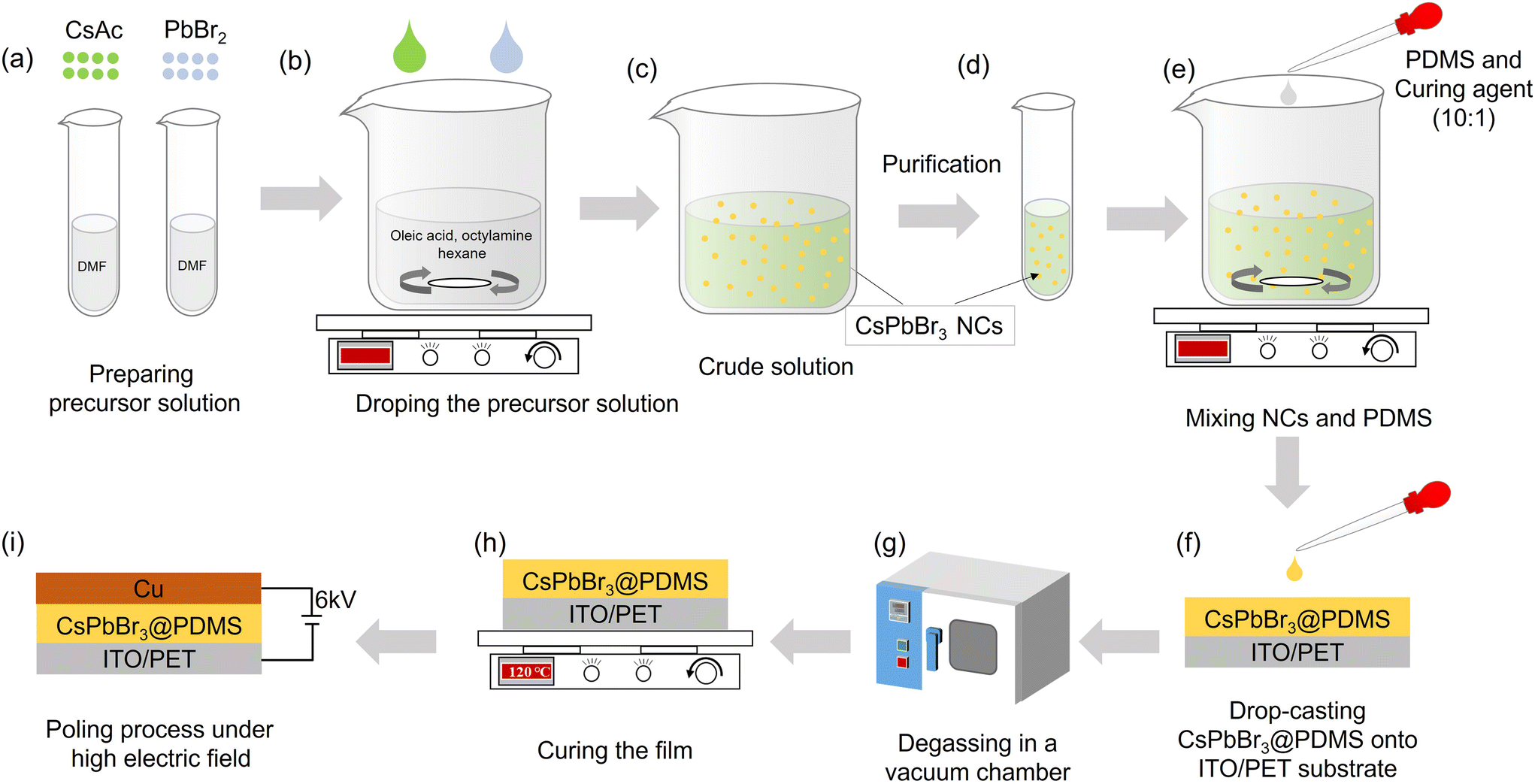 | ||
| Fig. 1 Schematic illustration outlining the entire fabrication process of PNG devices. (a–d) Synthesis process of CsPbBr3 NCs. (e–h) Fabrication process of the CsPbBr3@PDMS composite film. (i) Assembly and polarization of PNG devices. | ||
CsPbBr3 NCs were synthesized using the emulsion synthesis method, which enables large-scale production (0.5 g using 50 mL solution) in ambient air at room temperature. The left side of Fig. 2a displays a photograph of the yellow, dry solid CsPbBr3 NC powder, which emits bright green light under a UV lamp. This powder can be easily redissolved in hexane to form a CsPbBr3 NC solution. Fig. 2b shows the UV-vis absorption and PL spectra of the CsPbBr3 NC solution. The absorption spectra exhibit a clear exciton absorption peak at 500 nm, while the PL spectra show a narrow PL emission peak at 516 nm with a full width at half maximum (FWHM) of approximately 20 nm. The small Stokes shift of about 16 nm is characteristic of luminescent materials with excitons, indicating that the PL emission of CsPbBr3 NCs is primarily due to exciton recombination.30 The morphology of the CsPbBr3 NCs was investigated using transmission electron microscopy (TEM). Fig. 2c reveals that they are cubic-shaped and monodisperse, with an average size of 13 nm (Fig. S2†). X-ray diffraction (XRD) was used to evaluate the CsPbBr3 NCs@PDMS composite film at room temperature (Fig. 2d). The XRD patterns of the composite film can be indexed to the monoclinic phase of CsPbBr3 (JCPDS Card No. 18-0364), which is consistent with previous reports, indicating that the structure of the CsPbBr3 NCs maintains good stability during the entire fabrication process of the composite films.29,31 Other peaks come from PbBr2, possibly due to the low purity of the raw material. As shown in Fig. S3,† PbBr2 has no piezoelectric output. The composite films emit bright green light under a UV lamp, further demonstrating their good stability (Fig. S3†). Additionally, Fig. S4† shows that the surface of the composite films is smooth and dense, while the film without vacuum degassing treatment is rough and has many visible holes. This highlights the importance of vacuum degassing as a crucial step in the fabrication of high-quality composite films. The scanning electron microscopy (SEM) images of pure PDMS and composite films show that the addition of CsPbBr3 has no obvious effect on the structure and surface of PDMS (Fig. S5†). Furthermore, the CsPbBr3 NCs@PDMS composite film can be substantially bent by fingers, as shown on the right side of Fig. 2a, confirming its good flexibility and indicating its great potential for use in embedded and wearable electronics.
 | ||
| Fig. 2 (a) Photographs of CsPbBr3 NC powder taken under daylight and a UV lamp. (b) UV-vis absorption and PL emission spectra of a typical CsPbBr3 NC solution; inset shows the crystal lattice of the CsPbBr3 perovskite. (c) TEM image of CsPbBr3 NCs. (d) XRD pattern of the CsPbBr3 NCs@PDMS composite film. Standard XRD pattern of monoclinic CsPbBr3 corresponds to JCPDS Card No. 18-0364. | ||
Fig. 3a presents a schematic illustration of the fabricated CsPbBr3 NCs@PDMS composite-based PNG, which features a sandwich-type layered structure with copper and PET/ITO (ITO-coated PET plastic substrate) layers positioned on both sides of the composite film. Prior to delving into the specific performance of PNG devices, the power generation mechanism is briefly overviewed. To achieve high power generation performance, it is essential to subject the composite film, particularly the electric dipoles within it, to an electric polarization treatment before testing. As depicted in Fig. 3b, the electric dipoles in the CsPbBr3 NCs are randomly oriented within the composite film before any electrical polarization treatment is applied. However, after applying a high electric field to the electrodes on both sides of the composite film for a certain duration, the initially disordered dipoles in the CsPbBr3 NCs align in the same direction as the applied electric field, as shown in Fig. 3c. Some dipoles align perfectly with the electric field, while others are slightly tilted. Notably, each CsPbBr3 NC possesses a dipole component aligned along the direction of the electric field.32 When no external force is applied to the PNG device, the net dipole moment within the composite film remains zero, consequently yielding no electrical output signal. However, when a vertical downward force is exerted on the PNG (parallel to the direction of the electric dipoles), the stress triggers a polarization effect, prompting the electric dipoles in the CsPbBr3 NCs to abruptly align strongly in a uniform direction.33,34 In this manner, a negative charge accumulates at the top of the PNG device, while another negative charge accumulates at the bottom, leading to a notable piezoelectric potential in the direction of the applied force. In this scenario, positive and negative charges deliberately accumulate on the two electrodes to counteract the piezoelectric potential, ultimately causing the PNG device to generate voltage and current output signals (Fig. 3d).34 When the vertical downward force is released, the piezoelectric potential generated at the moment of release diminishes, and the accumulated charge on the electrode is transported in the opposite direction (Fig. 3e). Consequently, if the PNG device is subjected to continuous vertical compression, alternating current and voltage output signals can be observed.
 | ||
| Fig. 3 (a) Schematic diagram of the CsPbBr3 NCs@PDMS composite PNG. The arrangement of electric dipoles in CsPbBr3 NCs (b) before and (c) after high voltage polarization of the PNG device. Power generation under (d) pressing and (e) releasing modes of the PNG device. | ||
To validate the actual energy utilization scenario of CsPbBr3 NCs, we simulated the PNG model using the finite element method with COMSOL software. The PNG devices were simulated using adaptive piezoelectric materials with CsPbBr3 NC parameters. Specifically, we modeled square-shaped (100 μm × 100 μm) PDMS using a two-dimensional model. We constructed two models for simulation and comparison: a PNG based purely on PDMS and a composite device with 12 wt% CsPbBr3 NCs added to the PDMS matrix. To further investigate the piezoelectricity of the structure, we applied a constant external force of 1 GPa parallel to the polarization direction (perpendicular to the PNG device). The stress distribution and piezoelectric potential distribution between the copper electrode and the ITO electrode of the PNG device were obtained through simulation calculations, with the results represented in different colors. Both the pure PDMS-based PNG and PNG with CsPbBr3 NCs added to PDMS were evaluated. Compared to the calculated results obtained from the pure PDMS PNG (Fig. S6†), adding CsPbBr3 NCs to the PDMS matrix significantly affected the stress distribution and piezoelectric potential (Fig. 4a and b), resulting in a substantial enhancement of the piezoelectric potential. Subsequently, we investigated the effect of adding CsPbBr3 NCs on the performance of the assembled PNG devices. The device was placed on an electric shaker, and a metal block (cuboid, stainless steel) was placed on top to form a sandwich structure (see Fig. S7† for a schematic diagram of the test device). The frequency of the periodic mechanical vibration of the electric shaker could be set flexibly, and we tested the output voltage and current generated at different frequencies (10–50 Hz). For a PNG device based on a 12 wt% CsPbBr3@PDMS composite with an effective area of about 8 cm2, the maximum output peak-to-peak voltage and current recorded were 50 V and 5.5 μA, respectively, as shown in Fig. 4c and d (the testing conditions were 30 Hz and an applied force of 4.2 N). It is worth mentioning that all PNGs were polarized under a high voltage field. For comparison, we also tested the output voltage of the CsPbBr3 NC-based PNG device before high voltage polarization, which was about 4 V (Fig. S8a†). After high voltage polarization, the output voltage increased by ∼12 times, indicating that high voltage polarization is an essential step for assembling high-performance PNG devices. However, the current results were not sufficient to demonstrate that the high performance of the PNG devices was solely due to the addition of CsPbBr3 NCs. To further validate the contribution of CsPbBr3 NCs in the PNG devices, we measured the performance of a pure PDMS-based PNG under the same test parameters. The output peak-to-peak voltage of the PDMS-based PNG was only a negligible ∼1.8 V, much smaller than the 50 V of the CsPbBr3 NC-based PNG (Fig. S8b†). These results show that the addition of CsPbBr3 NCs is the fundamental reason for the significantly improved output performance of the PNG device. To verify that the output signal of the device was generated by the piezoelectric phenomenon, we also conducted a switching polarity test. A transfer switch was added to the test circuit. When the PNG device was connected forward, the output signal was positive. Pressing the switch button instantly reversed the connection, and the measured output signal was opposite (Fig. 4e). Obviously, this result demonstrates that the electrical signal is reversible, indicating that the output signal is generated by the compression motion straining the PNG device.35 Furthermore, during compression and release, a discernible difference in the peak value of the output signal can be observed, with variations of 14 V in output voltage and 1.3 μA in output current. This disparity arises from the differing strain rates experienced during the compression and release of stress on the PNG.32,36 As evident in Fig. 4f, as the frequency increases, the output voltage initially rises and then declines, peaking at 30 Hz, which aligns with the resonance state of the device system.37,38 In addition, increasing the applied force can increase the output voltage of the PNG device (Fig. S9†). These findings indicate that the assembled PNG device holds potential for applications in broadband and weak energy harvesting. Although the CsPbBr3 NCs@PDMS composite film is in a photoluminescent state and has no effect on the output of the PNG device (Fig. S10†), it can be expected that the excellent optical properties of CsPbBr3 NCs make it have great potential in the field of multi-functional energy harvesting devices.39–41
 | ||
| Fig. 4 COMSOL simulation of the CsPbBr3@PDMS composite film and experimentally measured output voltage and current of the PNG device. (a) The strain distribution and (b) piezo-potential distribution of the CsPbBr3@PDMS composite film with 12 wt% CsPbBr3 NCs. (c) Output voltage and (d) current from the CsPbBr3@PDMS composite PNG induced by periodic vertical compression. (e) Output switching test of output voltage. The insets show the magnified voltage or current output signals. (f) The output voltage of the PNG measured at different frequencies from 10 to 50 Hz. | ||
To further illustrate the practical utility of the assembled CsPbBr3 NCs@PDMS composite PNG, the device was vertically struck with a 300 g hammer, and capacitors of varying capacities were charged using the output electrical signal. As depicted in the circuit diagram in Fig. 5a, the voltage signal generated by the assembled PNG device was converted from alternating current to direct current using a bridge rectifier. Subsequently, the PNG device was periodically knocked vertically with a hammer at a frequency of approximately 2 times per second, and the generated output signal was rectified to charge capacitors with capacities of 1 μF and 3.3 μF, respectively. To monitor the capacitor charging process, it was connected to a multimeter, and the voltage was recorded every two seconds. Fig. 5b reveals that during periodic compression, the voltage across the capacitor increased linearly within the first 50 seconds. The energy conversion efficiency of the PNG device is 21.7% (see the ESI† for calculation details). The power density of the PNG device was analyzed by measuring the electrical parameters at both ends of the resistor. The external load range is from 1 MΩ to 1 GΩ, the current density drops from 350 nA cm−2 to 37.3 nA cm−2 and the voltage rises from 0.3 V to 30 V (Fig. 5c). The power density of the CsPbBr3 NCs@PDMS composite PNG device reaches a maximum value of 2.5 μW cm−2 at an external contact resistance of 100 MΩ (Fig. 5d).
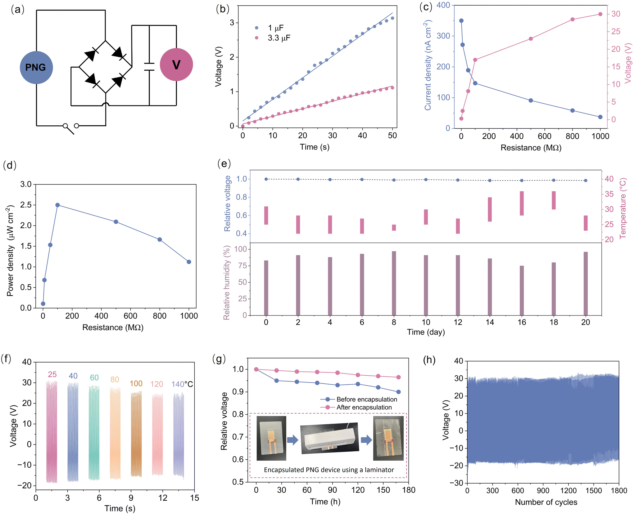 | ||
| Fig. 5 (a) Circuit diagram, where V represents a multimeter. (b) The tendency of the voltage at both ends of the capacitor to change with the time of the compressed PNG device. The straight line is a fitting line. (c) The current density, voltage and (d) power density of the PNG under different external load resistances from 1 MΩ to 1 GΩ. (e) The stability test of the PNG. The output voltage of the PNG was recorded at 30 Hz by using an electrodynamic shaker system. (f) The output voltage of the PNG at different temperatures. (g) The output voltage of the PNG in high humidity environments before and after encapsulation. Inset shows the process of encapsulation. (h) The durability test of the PNG. | ||
For electronic device applications, particularly PNG devices, it is crucial to exhibit not only excellent output performance but also long-term stability. To assess the stability of the PNG, the device was tested under air conditions every two days for a total of 20 days (June 20 to July 10), during the plum rain season characterized by high temperature and humidity in Nanjing. Notably, the output voltage remained at 98.5% of its initial value after 20 days (Fig. 5e) and remained at 94.5% after 60 days (Fig. S11†). These results indicate that the output performance of the CsPbBr3 NCs@PDMS composite PNG device was minimally affected by environmental factors such as humidity and temperature. However, the range of ambient temperature and humidity variation is limited. In order to verify the thermal stability and possible application under a harsh environment, the performance of the PNG was characterized by recording the voltage changes at higher temperatures and humidity. The voltage of the PNG at different temperatures from 20 to 140 °C was examined, showing that the output of the PNG decreases slightly with the change of temperature. The voltage of the PNG retains more than 80.5% (Fig. 5f) of its original value after being heated at 140 °C for 1 h, proving its applicability over a very large temperature range. The decline in the output performance may be attributed to the fact that CsPbBr3 is a thermally sensitive material, and the low melting point of the PET flexible electrode also makes its contact effect with the composite film worse at higher temperatures.8 The voltage of the PNG in high humidity environments (the relative humidity is 100%) was monitored, showing that the output of the PNG decreases as the storage time increases (Fig. 5g). The thin thickness of PNG devices allows them to be encapsulated using a laminator. Encapsulated PNG devices show better stability in high humidity environments (Fig. 5g). Finally, the long-term stability of the PNG was also investigated to confirm mechanical durability in periodic pressing and releasing modes with a mechanical force of 4.2 N. Fig. 5h illustrates the measured values for voltage, with no noticeable decrease in the output performance after more than 1800 cycles, confirming the good durability of the fabricated device. It is believed that the PDMS matrix bears most of the compressive force during compression, thereby minimizing strain on the CsPbBr3 NCs.33 Therefore, the CsPbBr3 NCs@PDMS composite PNG device effectively prevents fracture and cracking of the CsPbBr3 NCs embedded in the PDMS matrix under applied forces. Furthermore, due to the simple fabrication process, low cost, remarkable optical characteristics and long-term stability of composite PNG devices, they exhibit great potential for large-scale multifunctional piezoelectric energy harvesting applications.
Conclusions
In summary, we have successfully demonstrated a high-performance piezoelectric PNG based on monoclinic phase CsPbBr3 NCs embedded in a PDMS composite film. This represents the first report of a monoclinic phase CsPbBr3-based PNG. We have achieved an optimized running frequency of 30 Hz for this frequency-dependent PNG. When a force of 4.2 N is applied over an effective area of 8 cm2 at a frequency of 30 Hz, a peak-to-peak output voltage of 50 V, an output current of 5.5 μA and a power density of 2.5 μW cm−2 can be obtained. The alternating output signals generated by the PNG can be used to charge a capacitor through a bridge rectifier with a high energy conversion efficiency of 21.7%. The outputs are comparable to those of previously reported perovskite-PDMS-based devices (Table S1†), which supports the successful fabrication of an efficient PNG in the present study. Furthermore, the output voltage of the PNG remains at 98.5% of its initial value after 20 days, indicating excellent stability. This study highlights the great potential of CsPbBr3 perovskite materials for the simple and economical fabrication of high-performance piezoelectric energy harvesting devices.Author contributions
Jingkun Xu: conceptualization, methodology, formal analysis, data curation, software, writing – original draft, and visualization. Yechen Zhou and Kaiyan Zhu: investigation and writing – review and editing. Hao Jiang: data curation, software and writing – review and editing. Ying Wan, Min Lai and Shuhong Xu: writing – review and editing, supervision and resources.Data availability
The data supporting this article have been included as part of the ESI.†Conflicts of interest
There are no conflicts to declare.Acknowledgements
This work is supported by the Natural Science Foundation of China (No. 62275126 and 62305167), the Natural Science Foundation of the Jiangsu Higher Institution of China (No. 22KJB510032), and the Startup Foundation for Introducing Talent of Nanjing University of Information Science and Technology (No. 2022r031).References
- J. Luo and Z. L. Wang, Energy Storage Mater., 2019, 23, 617–628 CrossRef.
- M. A. Johar, A. Waseem, M. A. Hassan, I. V. Bagal, A. Abdullah, J. S. Ha and S. W. Ryu, Adv. Energy Mater., 2020, 10, 2002608 CrossRef CAS.
- H. C. Liu, J. W. Zhong, C. Lee, S. W. Lee and L. W. Lin, Appl. Phys. Rev., 2018, 5, 041306 Search PubMed.
- Z. L. Wang and J. Song, Science, 2006, 312, 242–246 CrossRef CAS.
- K. Shi, B. Sun, X. Huang and P. Jiang, Nano Energy, 2018, 52, 153–162 CrossRef CAS.
- C. H. Wang, W. S. Liao, Z. H. Lin, N. J. Ku, Y. C. Li, Y. C. Chen, Z. L. Wang and C. P. Liu, Adv. Energy Mater., 2014, 4, 1400392 CrossRef.
- K. I. Park, J. H. Son, G. T. Hwang, C. K. Jeong, J. Ryu, M. Koo, I. Choi, S. H. Lee, M. Byun, Z. L. Wang and K. J. Lee, Adv. Mater., 2014, 26, 2514–2520 CrossRef CAS PubMed.
- H. Chen, L. Zhou, Z. Fang, S. Wang, T. Yang, L. Zhu, X. Hou, H. Wang and Z. L. Wang, Adv. Funct. Mater., 2021, 31, 2011073 CrossRef CAS.
- X. Li, Y. Wu, S. Zhang, B. Cai, Y. Gu, J. Song and H. Zeng, Adv. Funct. Mater., 2016, 26, 2435–2445 CrossRef CAS.
- H. Zhou, Q. Chen, G. Li, S. Luo, T.-B. Song, H.-S. Duan, Z. Hong, J. You, Y. Liu and Y. Yang, Science, 2014, 345, 542–546 CAS.
- B. R. Sutherland and E. H. Sargent, Nat. Photonics, 2016, 10, 295–302 CAS.
- H. Wang and D. H. Kim, Chem. Soc. Rev., 2017, 46, 5204–5236 CAS.
- Y.-J. Kim, T.-V. Dang, H.-J. Choi, B.-J. Park, J.-H. Eom, H.-A. Song, D. Seol, Y. Kim, S.-H. Shin, J. Nah and S.-G. Yoon, J. Mater. Chem. A, 2016, 4, 756–763 CAS.
- R. Ding, H. Liu, X. Zhang, J. Xiao, R. Kishor, H. Sun, B. Zhu, G. Chen, F. Gao, X. Feng, J. Chen, X. Chen, X. Sun and Y. Zheng, Adv. Funct. Mater., 2016, 26, 7708–7716 CrossRef CAS.
- J. Tian, Q. Xue, Q. Yao, N. Li, C. J. Brabec and H. L. Yip, Adv. Energy Mater., 2020, 10, 2000183 CAS.
- Y.-Q. Zhao, Q.-R. Ma, B. Liu, Z.-L. Yu and M.-Q. Cai, Phys. Chem. Chem. Phys., 2018, 20, 14718–14724 CAS.
- D. B. Kim, K. H. Park and Y. S. Cho, Energy Environ. Sci., 2020, 13, 2077–2086 CAS.
- Y. Zhou and Y. Zhao, Energy Environ. Sci., 2019, 12, 1495–1511 CAS.
- Z. Wang, R. Fu, F. Li, H. Xie, P. He, Q. Sha, Z. Tang, N. Wang and H. Zhong, Adv. Funct. Mater., 2021, 31, 2010009 CAS.
- H. Liao, S. Guo, S. Cao, L. Wang, F. Gao, Z. Yang, J. Zheng and W. Yang, Adv. Opt. Mater., 2018, 6, 1800346 CrossRef.
- M. H. Bagheri, A. A. Khan, S. Shahzadi, M. M. Rana, M. S. Hasan and D. Ban, Nano Energy, 2024, 120, 109101 CrossRef CAS.
- S. Mondal, T. Paul, S. Maiti, B. K. Das and K. K. Chattopadhyay, Nano Energy, 2020, 74, 104870 CrossRef CAS.
- J. Nie, L. Zhu, W. Zhai, A. Berbille, L. Li and Z. L. Wang, ACS Appl. Electron. Mater., 2021, 3, 2136–2144 CrossRef CAS.
- S. Wu, F. Zabihi, R. Y. Yeap, M. R. Y. Darestani, A. Bahi, Z. Wan, S. Yang, P. Servati and F. K. Ko, ACS Nano, 2023, 17, 1022–1035 CrossRef CAS.
- Y. H. Lee, I. Shabbir, K. H. Yoo and T. W. Kim, Nano Energy, 2021, 85, 105975 CrossRef CAS.
- L. Xu, J. Chen, J. Song, J. Li, J. Xue, Y. Dong, B. Cai, Q. Shan, B. Han and H. Zeng, ACS Appl. Mater. Interfaces, 2017, 9, 26556–26564 CrossRef CAS PubMed.
- Y. Wu, Y. Ma, H. Zheng and S. Ramakrishna, Mater. Des., 2021, 211, 110164 CrossRef CAS.
- D. Zhang, S. Mandal, D. Y. Chung, J. Xu, N. Shan, M. G. Kanatzidis and M. Chen, Commun. Chem., 2024, 7, 175 CrossRef CAS PubMed.
- L. Yang, T. Wang, Q. Min, B. Liu, Z. Liu, X. Fan, J. Qiu, X. Xu, J. Yu and X. Yu, ACS Omega, 2019, 4, 6084–6091 CrossRef CAS.
- K. Zheng, Q. Zhu, M. Abdellah, M. E. Messing, W. Zhang, A. Generalov, Y. Niu, L. Ribaud, S. E. Canton and T. Pullerits, J. Phys. Chem. Lett., 2015, 6, 2969–2975 CrossRef CAS PubMed.
- G. Huang, C. Wang, S. Xu, S. Zong, J. Lu, Z. Wang, C. Lu and Y. Cui, Adv. Mater., 2017, 29, 1700095 CrossRef PubMed.
- J. H. Jung, M. Lee, H. Jung-Il, Y. Ding, C.-Y. Chen, L.-J. Chou and H. L. Wang, ACS Nano, 2011, 5, 10041–10046 CrossRef CAS.
- K. Y. Lee, D. Kim, J. H. Lee, T. Y. Kim, M. K. Gupta and S. W. Kim, Adv. Funct. Mater., 2013, 24, 37–43 CrossRef.
- M. K. Gupta, S.-W. Kim and B. Kumar, ACS Appl. Mater. Interfaces, 2016, 8, 1766–1773 CrossRef CAS.
- K. I. Park, M. Lee, Y. Liu, S. Moon, G. T. Hwang, G. Zhu, J. E. Kim, S. O. Kim, D. K. Kim, Z. L. Wang and K. J. Lee, Adv. Mater., 2012, 24, 2999–3004 CrossRef CAS PubMed.
- D. Kim, K. Y. Lee, M. K. Gupta, S. Majumder and S. W. Kim, Adv. Funct. Mater., 2014, 24, 6949–6955 CrossRef CAS.
- M. M. Rana, A. A. Khan, W. Zhu, M. F. A. Fattah, S. Kokilathasan, S. Rassel, R. Bernard, S. Ababou-Girard, P. Turban, S. Xu, C. Wang and D. Ban, Nano Energy, 2022, 101, 107631 CrossRef CAS.
- Y. Mao, P. Zhao, G. McConohy, H. Yang, Y. Tong and X. Wang, Adv. Energy Mater., 2014, 4, 1301624 CrossRef.
- P. Xia, H. Sun, S. Xu, T. Zhou, S. Zong, C. Lu and C. Wang, Adv. Energy Mater., 2023, 13, 2301332 CrossRef CAS.
- S. Pal, A. Ghorai, D. K. Goswami and S. K. Ray, Nano Energy, 2021, 87, 106200 CrossRef CAS.
- S. Pal, A. Ghorai, S. Mahato and S. K. Ray, Adv. Opt. Mater., 2023, 11, 2300233 CrossRef CAS.
Footnote |
| † Electronic supplementary information (ESI) available. See DOI: https://doi.org/10.1039/d4nr03579h |
| This journal is © The Royal Society of Chemistry 2025 |