
 Open Access Article
 This Open Access Article is licensed under a
 Creative Commons Attribution 3.0 Unported Licence
Investigation of Ti nanostructures via laboratory scanning-free GEXRF
Steffen
Staeck
 *a,
Jonas
Baumann†
a,
Philipp
Hönicke
bc,
Nils
Wauschkuhn
b,
Ferdinand
Spikermann
a,
Daniel
Grötzsch
a,
Holger
Stiel
d and
Birgit
Kanngießer
a
*a,
Jonas
Baumann†
a,
Philipp
Hönicke
bc,
Nils
Wauschkuhn
b,
Ferdinand
Spikermann
a,
Daniel
Grötzsch
a,
Holger
Stiel
d and
Birgit
Kanngießer
a
aTechnical University of Berlin, Hardenbergstraße 36, 10623 Berlin, Germany. E-mail: steffen.staeck@tu-berlin.de
bPhysikalisch-Technische Bundesanstalt, Abbestraße 2–12, 10587 Berlin, Germany
cHelmholtz-Zentrum Berlin, Hahn-Meitner-Platz 1, 14109 Berlin, Germany
dMax Born Institute, Max-Born-Straße 2A, 12489 Berlin, Germany
First published on 18th December 2024
Abstract
The ability to characterize periodic nanostructures in the laboratory gains more attention as nanotechnology is widely utilized in a variety of application fields. Scanning-free grazing-emission X-ray fluorescence spectroscopy (GEXRF) is a promising candidate to allow non-destructive, element-sensitive characterization of sample structures down to the nanometer range for process engineering. Adopting a complementary metal–oxide semiconductor (CMOS) detector to work energy-dispersively via single-photon detection, the whole range of emission angles of interest can be recorded at once. In this work, a setup based on a Cr X-ray tube and a CMOS detector is used to investigate two TiO2 nanogratings and a TiO2 layer sample in the tender X-ray range. The measurement results are compared to simulations of sample models based on known sample parameters. The fluorescence emission is simulated using the finite-element method together with a Maxwell-solver. In addition, a reconstruction of the sample model based on the measurement data is conducted to illustrate the feasibility of laboratory scanning-free GEXRF as a technique to non-destructively characterize periodic nanostructures in the tender X-ray range.
1. Introduction
Periodic nanostructures become more and more important in a multitude of application fields,1 for example energy materials,2,3 energy storage,4 optics5 or semiconductor devices.6 This increase in interest naturally demands the ability to reliably characterize these structures for development, process engineering and quality control with respect to their dimensional and compositional parameters. To this end, many established techniques can be employed.7 Microscopic techniques like scanning electron microscopy (SEM)8 or transmission electron microscopy (TEM)9 are able to deliver high-resolution images of the sample, but require sample preparation, which may include destroying the sample. Atomic force microscopy (AFM)10 on the other hand is limited by artifacts introduced by the shape of the tip used. One limitation inherent to all microscopic techniques is the inability to gain ensemble information, thus only a small segment of the sample can be analyzed. Photon-based techniques like grazing-incidence small angle X-ray scattering (GISAXS)11,12 or grazing-incidence X-ray fluorescence spectroscopy (GIXRF)13 are non-destructive, deliver ensemble information and in case of GIXRF, are element-sensitive. One major disadvantage of both techniques is the requirement on the coherence of the probing X-ray radiation, which renders the application in a laboratory setting challenging. Furthermore, the small angle of incidence of the X-ray radiation enlarges the excitation footprint, so that sub-mm scaled sample areas are very difficult to analyze.Grazing-emission X-ray fluorescence spectroscopy (GEXRF)14–17 circumvents both problems by measuring the angular dependence of the XRF signal in the detection channel rather than in the excitation channel. For this, the detection angle and thereby the information depth is tuned. Additionally, due to the self-interference of the fluorescence photons, the probability of XRF emission in the sample is spatially modulated at a nm-length scale, thus enhancing the spatial sensitivity of the method. Indeed, if different XRF lines can be distinguished by the detector and the angular resolution is sufficient, the coherence requirements in the detection channel are fulfilled. As for the excitation channel, there are no requirements regarding coherence, so a wide variety of X-ray sources may be used in GEXRF, also featuring focusing optics. This makes a laboratory application appealing, which also enables the use of GEXRF for process engineering. Scanning-free GEXRF utilizes a 2D pixel detector like a complementary metal–oxide semiconductor (CMOS) detector. This way, the whole angular range of interest can be recorded at once, while the angular resolution can be sufficiently small (depending on the pixel size and distance). The feasibility of the method has already been established with various measurements at synchrotron radiation facilities as well as in the laboratory.18–20 This work aims to demonstrate and assess the applicability of the method in the tender X-ray range (≈1 to several keV), using stable and relatively low-cost laboratory X-ray sources and detectors.
As a demonstration sample, different TiO2 nanostructures with a thin HfO2 surface coating layer are investigated. Even though the sample system was manufactured for demonstration purposes, it resembles transistor structures consisting of Si fins.21 The sample was measured in prior studies and is thus well known. Because of this and its resemblance of actual industry samples, it is ideal to investigate the feasibility of laboratory GEXRF and its sources of systematic uncertainty like limited photon statistics or limited angular resolution. Furthermore, it can be utilized as a reference sample for future measurements. The GEXRF measurement results are compared to simulations based on known parameters from prior measurements19 and in case of one nanograting, a reconstruction of the sample model is performed to discuss the feasibility of the method in the laboratory. This is to the authors’ knowledge the first time a reconstruction of a 2D nanostructure is performed using laboratory GEXRF. The measurements further demonstrate, that the GPixel GSENSE 400 BSI CMOS chip22 can be employed in the tender X-ray range, as long as the photon flux is sufficiently low to prevent radiation damage.23
2. Experimental
The investigated sample consists of a silicon wafer, on top of which a TiO2 layer has been deposited. A grating structure was etched into the sample, resulting in five stripes with varying linewidths and resulting from that, varying etching depths. In some cases, the etching depth exceeds the TiO2 layer and extends the grating structure into the Si wafer. Afterwards, a HfO2 capping layer was added. One of those five sample stripes has been well characterized in previous measurements,19 henceforth referred to as stripe 5. The gratings are manufactured with a nominal pitch of 123 nm. A picture of the sample wafer and a schematic cross section of the sample are shown in Fig. 1. The two other sample stripes investigated in this work consist of a grating structure with a greater linewidth and lower etching depth (stripe 3) than the one already mentioned and an area of the sample without any etching at all (stripe 1), which also have been measured in the PTB laboratory at the BESSY II synchrotron radiation facility and are used as a reference in this work.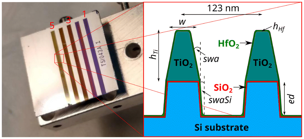 | ||
| Fig. 1 On the left, a picture of the sample wafer is shown with the five different sample stripes visible. Stripe 1 denotes the unetched sample, while 3 marks the lesser etched and 5 the greater etched grating structure. On the right, a schematic cross section of the TiO2 gratings with the parameters defining the sample model is shown. Only two of the approximately 8000 grating lines in the 1 mm wide stripe are shown. The sample model consists of a Si substrate with a SiO2 top layer. On top of this a TiO2 layer is located. A grating structure is etched into the layered sample, the grating lines may protrude into the Si substrate. The resulting structure is then covered by a HfO2 layer. The etching depth varies between the different sample stripes. | ||
The experimental setup is composed of an ultra-high vacuum (UHV) chamber, in which a goniometer for sample positioning and alignment is located. The X-ray source, the sample and the detector are placed in 90° geometry, with 90° between the source-to-sample and sample-to-detector axes (see Fig. 2b). The X-ray tube used as the radiation source features a Cr anode and is operated with 50 kV tube voltage and 270 μA anode current. The polychromatic radiation is focused on the sample with a polycapillary lens with peak transmittivity at around 8 keV. The spot size on the sample is approximately 800 μm at Cr Kα.24 From measuring a known multilayer sample,25 the distance between sample and detector is calculated to be 51 cm. The detector used is a Tucson Dhyana 95 CMOS detector featuring the GPixel GSENSE 400 BSI CMOS chip, adapted for use with vacuum chambers.26 A setup schematic together with a schematic drawing of the geometry regarding the emission angles θ and φ is shown in Fig. 2. A 500 μm wide slit is placed in front of the sample to narrow down the spot size, which on the one hand prevents significant illumination of the areas next to the stripes and on the other hand limits the negative effects of the extended footprint on the angular resolution. For all measurements, the detector is cooled down to −15 °C and operated in the low-gain HDR mode.
 | ||
| Fig. 2 (a) Schematic drawing of the setup geometry with the emission angles θ and φ. (b) Schematic top view of the setup. The UHV chamber with the sample inside is shown as well as the Cr X-ray tube with the polycapillary lens to focus the radiation as well as the Tucsen Dhyana 95 CMOS detector. The CMOS is mounted on the outside of the UHV chamber via an adapter flange. | ||
3. Simulations
For the simulation of the layered structure without any lateral nanostructuring such as stripe 1, the Sherman equation with the approach of Urbach and de Bokx27,28 can be used to simulate the experimental data. However, to simulate the angular dependent XRF signal of a regularly nanostructured sample surface, these standard approaches for layered systems fail as already shown in Soltwisch et al.29 To address this, the principle of micro reversibility is applied.30 This principle states, that the electric field from a source measured at a detector position is the same, if detector and source exchange positions, thus depending only on the path, but not the path direction. Applied to GEXRF, this means that the electric field at the detector originating from a source (an atom) in the sample can be calculated by locating the source at the detector position and calculating the electric field in the sample. In other words, the GEXRF data can be calculated by treating it as if it was a grazing incident experiment. The advantage of this perspective is, that existing computer codes for such problems can be applied. Here, the Maxwell solver from JCMwave31 is used, as it was already applied in earlier works.19,29 It is important to note that for this calculation, the photon energy of the fluorescence radiation of interest governs the interference characteristics, whereas in a real GIXRF experiment the excitation photon energy is decisive. Another aspect for the GEXRF calculation to be considered is the absorption of the excitation radiation before it can excite atoms in the sample for fluorescence production. In our case, the low total height of the nanostructures and their composition led to negligible absorption, allowing to assume a uniform excitation strength of the sample atoms. Therefore, the angular modulation of the fluorescence signal is only dependent on the XSW field. Otherwise, the absorption of the exciting radiation has to be taken into account using the Sherman equation.27,32As the TiO2 grating structures have already been characterized from measurements at the synchrotron radiation facility BESSY II,19 the recorded Ti Kα fluorescence emission patterns can be compared to the simulated ones using the sample parameters from the previous work. The fluorescence emission of the nanostructures at a given set of θ and φ is calculated using a finite-element method (FEM). In this approach, a cross section of the nanostructure is parameterized and defined as the computational volume. The boundary conditions to the left and right are periodic as nominally identical grating lines are repeatedly patterned in a wide area. The boundary conditions above and below the nanograting are transparent as the vacuum and silicon are practically of infinite thickness. For each material in the nanostructure a separate domain is defined as the different materials have different optical properties. The cross section is then meshed into sufficiently small elements, for which a vectorial ansatz function can be defined by means of polynomials with a fixed order. The approximate electric field solution is the superposition of these local ansatz functions. In a last step, the calculated electric field is then numerically integrated within a specific domain to derive the corresponding relative fluorescence signal strength from this domain. As the electric field distribution inside the nanostructure is strongly dependent on the specific θ and φ coordinate, a separate calculation has to be performed for each angular coordinate. Angular-dependent fluorescence maps for Ti Kα dependent on the emission angles θ and φ with 61 × 124 data points are calculated for the evaluation of the results of stripe 3 and 5. The maps range from θ = 0° to θ = 1.2° and φ = −1.23° to φ = 1.23°. Due to the symmetry in the φ-direction, it is sufficient to calculate only one half of the maps. The angular resolution is Δθ = Δφ = 0.02°. In case of parameter determination of the sample structure from the measured angular maps, a non-linear regression is usually performed for the reconstruction. Due to the computational costly FEM calculation and the complex behaviour of the χ2 surface (sum of the weighted squared difference of forward simulation and measured XRF map), the reconstruction is performed using Bayesian optimization.32
4. Evaluation
The evaluation of the recorded CMOS frames is performed via single-photon event analysis with the clustering algorithm. The electron charge and thus the displayed analogue-to-digital units (ADU), which are generated when absorbing an X-ray photon, are proportional to the photon energy. An algorithm searches the background-subtracted frames for pixels exceeding a first intensity threshold T1 multiplied by the individual pixel dark noise σp and marks those pixels as part of a photon event. The neighboring pixels are iteratively searched for exceeding a second threshold T2 × σp and then added to the event. This way, photon events spread over several pixels can be detected and their spatial and energy information obtained. For this measurement, thresholds of T1 = 6 and T2 = 3 are applied. The algorithm is explained in more detail in ref. 33 and available at GitHub (see Data Availability section). All events from all frames of one measurement are then depicted in an energy-dispersive spectrum. A fluorescence line of interest, in this case the Ti Kα line, is chosen and a region-of-interest (ROI) is set with lower and upper bounds for the photon energy. All photons within this ROI are further evaluated with respect to their angular information. To retrieve the angular information, the position of each photon needs to be translated to the meridional emission angle θ and a sagittal angle φ perpendicular to the former one. This can be accomplished by vector calculation, if the geometry of the detector with respect to the excitation spot on the sample is known. Parameters of special interest are the sample to detector distance, the position on the CMOS chip, where the emission angle is exactly θ0 = 0°, and the tilt of the sample surface in relation to the chip. The distance is gained from measuring a reference sample, as described in section 2, while the other parameters are adjusted manually by matching the measurement results to previous synchrotron facility measurements. The measurement of the reference sample as well as the manual matching of the angular scale with the help of the synchrotron data could be avoided if the setup geometry was well-known. There are various means to perform a reference-free angular calibration, for example a laser could be employed to measure the distance from the sample to the detector via the movement of its reflexes on the detector frame when the sample is tilted. The position of the unreflected beam could be used as the reference position of θ0 = 0°, when the sample was aligned parallel to the beam. This procedure was already performed before,34 but could not be applied in this measurement series with the required angular accuracy. However, with some improvements, especially to the laser's focal spot size, this angular calibration method should be feasible. Another approach, avoiding the laser, consists of the measurement of a crystalline sample with known structure and orientation. Then the prominent Bragg peaks on the detector can be used for the determination of the geometry. In the end, it might be that a combination of approaches including the usage of reference samples provides the best results on precision and accuracy. With the geometry known, the pixel positions of the photons included in the ROI can be translated into θ and φ values. φ0 = 0° is determined by matching it to the symmetry axis of the recorded fluorescence pattern. With this information, so-called θ–φ-maps can be calculated, where the fluorescence intensity of the Ti Kα line is depicted in dependence on the emission angles. In case of the one-dimensional emission pattern of the layered sample, an in-house deconvolution software called Specfit is utilized to further reduce the contribution of background noise to the GEXRF signal. For this, the pixels of the CMOS frames are assigned to different discretized emission angles of θ and an energy-dispersive spectrum is calculated for each value of θ. Each spectrum then is deconvoluted by fitting the fluorescence peaks after a background subtraction via stripping was performed. Finally, the Ti Kα signal is plotted over the θ emission angle.5. Results
The results for the three measured sample stripes are presented and discussed in this section. For the non-etched stripe 1 and the lesser etched stripe 3, the results will be compared to results previously obtained by measurements performed by the Physikalisch-Technische Bundesanstalt (PTB) at the BESSY II synchrotron radiation facility. For stripe 5, already investigated in ref. 19, the optimization results for the JCMwave simulation are shown and discussed.5.1. Stripe 1
To illustrate the challenges involved in investigating two-dimensional nanostructures with GEXRF, this unetched part of the sample wafer was measured. It does not have any two-dimensional structural features, so the fluorescence interference pattern does exhibit only a modulation of the signal in the direction of the emission angle θ. Hence, the emission signal can be integrated along pixels of similar θ angle for increased statistics, reducing the necessary measurement time drastically. 147![[thin space (1/6-em)]](https://www.rsc.org/images/entities/char_2009.gif) 600 frames with an exposure time of 500 ms have been recorded with a total measurement time of ca. 20.5 h. Two hundred dark frames are recorded for background subtraction. A reduced data set of only 1% or about 12 min measurement time is evaluated as well for comparison. The sample-detector distance of the setup is known from measuring the reference multilayer sample, but the absolute angular scale is still unknown and therefore the angle of θ0 = 0° has to be fitted. However, the angular position of the rise of intensity of the fluorescence profile is strongly dependent on the optical density and therefore the elemental density of the TiO2 and HfO2 present in the sample. These densities typically differ for nanostructures as compared to their bulk values due to significant surface-to-volume ratios. Therefore, the β and δ values of the refractive index for the TiO2 and HfO2 layers have been taken from previous synchrotron radiation facility measurements. They both differ from their literature values35 by a factor of 0.9. A scaling factor for the fluorescence intensity is fitted as well as the width of a Gaussian, with which the simulated data is convoluted to account for setup efficiency and angular broadening in the data, respectively. The sample parameters fitted are the TiO2 and HfO2 layer thicknesses. The results of the measurements and the fits are displayed in Fig. 3.
600 frames with an exposure time of 500 ms have been recorded with a total measurement time of ca. 20.5 h. Two hundred dark frames are recorded for background subtraction. A reduced data set of only 1% or about 12 min measurement time is evaluated as well for comparison. The sample-detector distance of the setup is known from measuring the reference multilayer sample, but the absolute angular scale is still unknown and therefore the angle of θ0 = 0° has to be fitted. However, the angular position of the rise of intensity of the fluorescence profile is strongly dependent on the optical density and therefore the elemental density of the TiO2 and HfO2 present in the sample. These densities typically differ for nanostructures as compared to their bulk values due to significant surface-to-volume ratios. Therefore, the β and δ values of the refractive index for the TiO2 and HfO2 layers have been taken from previous synchrotron radiation facility measurements. They both differ from their literature values35 by a factor of 0.9. A scaling factor for the fluorescence intensity is fitted as well as the width of a Gaussian, with which the simulated data is convoluted to account for setup efficiency and angular broadening in the data, respectively. The sample parameters fitted are the TiO2 and HfO2 layer thicknesses. The results of the measurements and the fits are displayed in Fig. 3.
 | ||
| Fig. 3 (a) Measured angle-dependent Ti Kα fluorescence emission profile of the layered sample in orange with the full data of 20.5 h measurement time. The error bars depict the statistical uncertainties originating from the total photon counts of each emission angle. (b) The same measurement utilizing only the first 12 min of the full data set and the respective fit. | ||
The fit matches the data rather well for both data sets. The profile of the reduced data is very noisy, which is expected with the very limited effective measurement time. Nonetheless, for both cases the fit produces similar results, the uncertainties given are the fit standard deviations. They are hTi = 55.5 ± 0.7 nm and hHf = 3.03 ± 0.07 nm for the full dataset as well as hTi = 55.3 ± 1.2 nm and hHf = 3.14 ± 0.11 nm for the reduced one. The results confirm that scanning-free GEXRF with the presented laboratory setup is able to investigate one-dimensional layered structures and showcases that even a very limited measurement can produce precise results, when dealing with a simple one-dimensional layered sample. The necessary measurement time to achieve sufficient statistics increases drastically, when a two-dimensional fluorescence pattern has to be recorded, as will be shown in the next section.
5.2. Stripe 3
The second part of the sample investigated in this work is a grating etched into the layered sample structure, similar to that displayed in Fig. 1. Altogether, 295200 frames with an exposure time of 500 ms have been recorded, totaling to a measurement time of 41 h. A total of 1400 dark frames have been recorded for background subtraction. The sample-detector distance was again determined via measuring the multilayer reference sample. The position of θ0 = 0° was established by matching the data to the simulation, while the position of the symmetry axis of φ0 = 0° was determined manually. Since the sample holder had to be removed from the vacuum chamber to adjust the slit in front of the sample wafer to the current sample stripe, the calibration regarding the position of θ0 = 0° and φ0 = 0° had to be repeated for each sample stripe. The fluorescence interference pattern of the Ti Kα line was simulated based on a sample model with the parameters hTi = 51.3 nm, hHf = 2.9 nm, ρTi = 0.90 × 4.2 g cm−3, ρHf = 0.74 × 9.68 g cm−3, ed = −20.5 nm, w = 75.2 nm, swa = 15.5° and swaSi = 7.7° (see Fig. 1 for reference). The parameters have been gained from the sample reconstruction based on data from a synchrotron radiation facility measurement. The comparison is shown in Fig. 4.
 | ||
| Fig. 4 (a) Measured and simulated θ–φ-maps of the Ti Kα fluorescence intensity for the TiO2 grating with intermediate etching depth. The measured data has been mirrored along the φ symmetry axis to increase the available photon count and statistics. The JCMwave simulation on the right side is normalized to the measured data. The width of each data point in the θ–φ-maps is 0.02°. For normalization, the mean value of the map between 1.5° ≤ θ ≤ 1.9° and 0.7° ≤ φ ≤ 1.5° has been used. An offset has been subtracted from the measured map to account for scattered radiation. It was determined using the median value of the area between 0.05° ≤ θ ≤ 0.15° and −0.1° ≤ φ ≤ 0.1°. The position of the presented θ- and φ-data points in (b) are indicated by the red and orange dots. In (b), the angular profiles for several values of θ and φ are shown for the measured data and the simulation. The error bars indicate the statistical uncertainties of the measured values. Since the measurement data has been mirrored along φ0 = 0° and the simulation is symmetric anyways, it is sufficient to show the profiles along the φ axis only for positive values. | ||
The results show good agreement between the simulation and the measurement data. The features visible in the simulation are present in the measurement as well, although the data is still quite noisy due to the lacking photon statistics. Some features are not as clearly visible as they are in the simulation, as can be seen in Fig. 4(b). This can be attributed to statistical limitations, the angular resolution and manufacturing uncertainties within the sample itself, such as linewidth, etch depth and line edge roughness as already discussed in Hönicke et al.19 Those parameters vary locally along the grating structure, effectively broadening certain features in the θ–φ-map when using an extended excitation footprint like in these measurements. The statistical errors are too small to explain every deviation, so the latter two effects are the dominant effects causing this. That said, the data shows that results gained from synchrotron radiation facility measurements are reproducible in the laboratory, although with limitations, especially regarding the photon flux, measurement time and photon statistics.
5.3. Stripe 5
This part of the sample structure has already been measured and analyzed in the work of Hönicke et al.19 The sample structure is depicted in Fig. 1 and is similar to the etched sample stripe discussed before, but it features a greater etching depth. The reconstructed sample parameters with their respective confidence intervals are a TiO2 lineheight of hTi = 55.3(5) nm, a linewidth of w = 37.7(3) nm and a HfO2 layer thickness of hHf = 2.3(08) nm. The nominal grating pitch of 123 nm was not determined and also will be treated as constant in this work. In this measurement, 514414 frames at 500 ms have been recorded with 400 dark frames, with a total measurement time of 70 h. With the recorded data, the sample model was then reconstructed with a JCMwave finite-element simulation, using a Bayesian optimization algorithm. For the optimization process, only certain data points at fixed values for θ and φ were used to limit the required computational effort. From the resulting parameters and sample model, a θ–φ-map has been calculated and is compared to the measured data in Fig. 5(a). The data points, which were used for the optimization process, are marked by the red and orange dots in the map.
 | ||
| Fig. 5 (a) Measured and reconstructed θ–φ-maps of the Ti Kα fluorescence intensity for the TiO2 grating with greater etching depth, similar to Fig. 4. The point of θ0 = 0° was determined matching the fluorescence pattern to existing data from Hönicke et al.19 The locations of the data points used for the optimization process are marked by the red and orange dots. Additionally, an offset in both angular directions has been determined in the optimization process to account for minor errors in the calibration process. In (b) the data points used for the reconstruction process of the recorded Ti Kα fluorescence intensity pattern are depicted together with the simulation results from the optimization for stripe 5. The error bars indicate the statistical uncertainties of the measured values. Since the measurement data has been mirrored along φ0 = 0° and the simulation is symmetric anyways, it is sufficient to show the profiles along the φ axis only for positive values. | ||
The reconstructed map resembles the measurement quite well. The most obvious deviations occur at the first intensity maximum at θ = 0.34°, where the measurement data is lacking intensity and contrast compared to the simulation. This can also be seen in the profiles on the right-hand side. Overall, the measured map appears noisy due the limited photon statistics. This also contributes to the reduced contrast, but again, the limited angular resolution and spatial irregularities in the grating structure cause this effect as well.
The actual data which has been used for the optimization process and the reconstruction results are presented in Fig. 5(b). They consist of six profiles along certain θ- and φ-values, since an optimization utilizing the whole map requires too much computation effort. Thus, these data points have been chosen because of experiences from previous work,19 where they displayed increased sensitivity to changes in the model parameters.
Analogous to the complete fluorescence interference pattern, the reconstructed angular Ti Kα emission profiles fit satisfactorily to the measured data, although the increase of intensity along the φ axis at θ = 0.34° is not as well reproduced. This is to some extent also visible in the profile at θ = 0.4°. Some smaller features are not visible in the measured data, which are in the reconstruction, for example the pre-peak feature at θ = 0.25° in the profile for φ = 0.49°. Damping effects like this originate from limited angular resolution, photon statistics and structural irregularities of the sample.
The reconstructed parameters are shown in Table 1 and compared to the values gained in previous work.19 The relative deviations of the parameters to the synchrotron results are furthermore visualized in Fig. 6. The values for the angular offsets have only been optimized for the laboratory data. For some parameters an estimation of the uncertainties has been performed. They are estimated from the estimated uncertainty of the θ axis calibration of 0.01°. This estimation is based on the angular calibration that was performed beforehand. The correlations between the fitted θ offset and the other fit parameters obtained from the fit procedure are used to estimate the other confidence intervals. However, this was only possible for parameters exhibiting a correlation. For the rest of the parameters, estimated relative uncertainties in the range of 5–10% can be assumed. This estimation is gained from the deviation of the presented results from previous optimization attempts and the results of the synchrotron measurements. The confidence intervals of the synchrotron parameters are based on the reconstruction process alone and therefore are smaller than the uncertainties of the laboratory measurement. Taking the angular uncertainties into account would most probably lead to larger uncertainties for the synchrotron data as well.
 | ||
| Fig. 6 Visualization of the reconstruction results for the parameters of stripe 5. Depicted are the relative deviations of the laboratory results to the established synchrotron results. The uncertainties of the respective parameters are depicted in red, if uncertainties could be established. | ||
| Parameter | Lab. (uncertainty) | Synch. (conf. int.) |
|---|---|---|
| Lineheight (hTi)/nm | 58 (6) | 55.3 (5) |
| Linewidth (w)/nm | 43 (3) | 37.7 (3) |
| HfO2 thickness (hHf)/nm | 2.3 | 2.30 (8) |
| Sidewall angle (swa)/° | 11 (3) | 12.4 (3) |
| Sidewall angle Si (swaSi)/° | 7.7 | 5.6 (3) |
| Overetching depth (ed)/nm | −49.7 | −55.7 (14) |
| Rel. ρTiO2 | 0.88 (5) | 0.89 |
| Rel. ρHfO2 | 0.84 | 0.83 |
| Offset θ/° | 0.0053 | |
| Offset φ/° | 0.0063 |
The reconstructed parameters are in reasonable agreement with the parameters gained from the synchrotron radiation facility reconstruction and show that it is feasible to perform a reconstruction based on laboratory data. Nevertheless, the results differ from the synchrotron results by several nanometers or degrees. In general, the previous measurements should be considered more trustworthy, since both statistics and angular resolution are superior to the ones presented here. The larger excitation footprint as compared to the synchrotron experiment (800 μm × 500 μm compared to 300 μm × 300 μm) pronounces spatial variations in the sample structure, as the reconstructed result represents an averaged nanostructure within the probed area. As already pointed out in the earlier work,19 the nanograting shows varying dimensional parameters along the stripe, which originate from etch inhomogeneities. Since the exact same measurement position and spot size and thus the resulting averaged nanostructure within the field of view is not the same, this explains part of the deviations. These different fields of view also result in different divergence amplitudes in the experimental data, which is not taken into account in the reconstruction, but still may influence the derived results. Moreover, the referenced synchrotron experiments from the previous work were performed on a freshly produced sample. Since then, this sample has been subject to many different experiments, where contamination, especially carbon growth, can occur. As this can significantly influence the reconstruction results,32 it is highly likely that it also has an influence here. Mainly the derived etch depth may be affected by carbon growth in the grooves. Furthermore, the uncertainties related to the determination of the angular θ and φ coordinates directly affect the reconstructed nanostructure parameters. The highest deviation is displayed by the linewidth w, differing about 5 nm. This parameter is especially sensitive to uncertainties or variations in the angular scale. Further disagreement is visible in the sidewall angles swa and swaSi. The uncertainty of the laboratory result for the swa angle at least includes its synchrotron counterpart. In case of the sidewall angle of the exposed silicon, the deviation might be explained by the missing elemental sensitivity to silicon. Analyzing the Si Kα signal as well might mitigate this problem, but also the sidewall angle of the Ti structure shows this deviation. Using more data points for the reconstruction or another set of data points may increase the sensitivity to these parameters.
Addressing these aspects is certainly a part of future work employing the GEXRF technique to nanostructure characterization both at a synchrotron and with laboratory sources. Especially the high sensitivity of the reconstruction results to possible inconsistencies of the calculated angular coordinates requires a more accurate determination of the experimental geometry. For laboratory source experiments, a further decrease in excitation spot size and a further increase in usable photon flux will help to avoid averaging over a large probing area and to reduce the noise level on the experimental data. In addition, a benchmark experiment employing identical and uncontaminated samples would allow to get rid of the potential impacts of the contamination on reconstructed parameters.
6. Conclusions
Scanning-free GEXRF was performed in the laboratory using a Cr X-ray tube and a CMOS detector for the investigation of a set of Ti nanostructure samples. A layered sample was investigated and its angular profile of the Ti Kα fluorescence emission line fitted. The results were compared to previous measurements at a synchrotron radiation facility. A second sample structure, a TiO2 grating, was measured and the data was also compared to synchrotron measurements. The third structure investigated is another TiO2 grating, which is well-known from previous measurements.19 The sample model was reconstructed using simulations based on the finite-element method and a Maxwell solver, while Bayesian optimization is used for the optimization process itself. The reconstructed parameters were compared to the established parameters and in general exhibit acceptable agreement. Especially the parameters describing the sidewall angles of the grating and the grating linewidth show some deviations from the synchrotron data. Uncertainties could be established for some parameters based on the uncertainty of the angular calibration of the θ angle and its correlation with other parameters. The deviations of the parameters from the previous results can be explained by the larger excitation footprint in the recent measurement and spatial variations of the sample, limited photon statistics and angular resolution and sample contamination.The results showcase the potential of laboratory scanning-free GEXRF for the non-destructive investigation of periodic nanostructures with nanometer resolution. For the first time a full reconstruction of a 2D nanosample via GERXF has been performed in the laboratory. While the setup exhibits good long-term stability, photon statistics and the angular resolution limit the analytical potential of the presented measurement and have to be addressed for future measurements and setups. The reconstructed sample parameters are mostly close to those gained from synchrotron radiation facility measurements and the reconstructed fluorescence emission pattern is in good agreement with the measurement data, considering the challenging sample system and off-the-shelf equipment. Furthermore, it is shown that the Tucsen Dhyana 95 CMOS detector might as well be employed in the tender X-ray range, as long as the photon flux is limited to prevent radiation damage.23 However, the use of this CMOS detector in the tender X-ray range is debatable, since the advantage of a significantly reduced readout time is offset by the lacking quantum efficiency (QE) compared to more common charge-coupled devices (CCD). One obvious improvement would be to utilize a detector featuring a thicker chip and higher QE, while maintaining a high framerate.36,37 Despite this, this CMOS detector offers a cost-effective way to cover the soft and tender X-ray range when performing single-photon-based measurements, featuring sufficient energy resolution and a negligible readout time.
Future improvements to the setup and measuring process may include the introduction of a reference-free angular calibration routine to enhance the accuracy of the reconstruction algorithm by omitting additional optimization parameters and to speed up the total measurement process without measuring a reference sample first. Complementary analysis of multiple fluorescence emission lines may improve the accuracy of the reconstruction as well. Addressing the most obvious limitations with the current laboratory setup, the photon flux as well as the angular resolution can be improved by utilizing optimized X-ray optics. The currently used polycapillary lens features a transmittance of 19.2% and a solid angle of acceptance of 7.4 msr24 at Cr Kα at 5.415 keV. This yields a transmission normalized to the solid angle of acceptance of 1.42 msr for this energy. Similar values for the normalized transmission can be achieved38 for focal spot sizes well below 100 μm. This means the slit in front of the sample to define the excitation spot could be omitted without a loss of total excitation flux, although a change of the working distance of the polycapillary lens would be necessary. The excitation spot diameter at Cr Kα should be at around 800 μm24 and the slit used is 500 μm in the current setup. For a Gaussian excitation spot shape, an increase of roughly 30% could be achieved, if the slit is omitted. If the X-ray beam is not aligned perfectly with the slit, the potential increase in flux is even higher. A purpose-built setup could feature a different excitation source, like a rotating-anode type X-ray tube.39 A rotating Cu anode X-ray tube with a tube voltage of 40 kV and an anode current of 30 mA40 paired with the polycapillary lens currently in use could be considered. The polycapillary lens features almost the same transmittance for Cr Kα as for Cu Kα.24 Simulating the Ti Kα fluorescence emission from a 25 nm thick TiO2 layer based on the calculated X-ray tube spectra by Ebel41 and the fundamental parameters of Elam et al.42 and Ebel et al.,43 the Cu rotating anode X-ray tube will increase the fluorescence flux by a factor of 29 compared to the currently used Cr X-ray tube. Utilizing a detector with a thicker chip will result in an improved QE. Already at 40 μm chip thickness, the theoretical QE is 95% for the Ti Kα line at 4.511 keV, for even thicker hybrid pixel detector chips it is almost 100%.44,45 The current Tucsen Dhyana 95 CMOS chip with a thickness of 10 μm only achieves a theoretical QE of around 50% at that photon energy, so employing a different detector could improve the detection efficiency by a factor of 2. Addressing all these possible improvements, a total measurement time reduction by a factor of at least 75 should be feasible, reducing the total measurement time for stripe 5 from 70 h to about 1 h. This way, routine laboratory GEXRF measurements of periodic nanostructures would be possible in a couple of hours, for example for process engineering, provided the computational power at hand is not limiting the analytical process. Being able to utilize the whole fluorescence pattern for the reconstruction might lower the requirements on photon statistics and measurement time. Here, tailored machine learning models can be expected to drastically cut down nowadays optimization times for specific sample systems.
Author contributions
Steffen Staeck: data curation, formal analysis, investigation, visualization, writing – original draft. Jonas Baumann: conceptualization, methodology, software, supervision, writing – review & editing. Philipp Hönicke: conceptualization, formal analysis, methodology, software, resources, validation, writing – review & editing. Nils Wauschkuhn: formal analysis, software. Ferdinand Spikermann: investigation. Daniel Grötzsch: resources. Holger Stiel: resources. Birgit Kanngießer: project administration, supervision.Data availability
Data for this article, including the results of the single-photon event evaluation process, is available at Zenodo at https://zenodo.org/doi/10.5281/zenodo.11549767. The source code for the single-photon event evaluation can be found at https://github.com/jonasbaumann13/SPE.Conflicts of interest
There are no conflicts to declare.Acknowledgements
The authors like to thank Frank Förste for the continuing support with the SpecFit software.References
- H. Yin, K. Xing, Y. Zhang, D. M. A. S. Dissanayake, Z. Lu, H. Zhao, Z. Zeng, J.-H. Yun, D.-C. Qi and Z. Yin, Chem. Soc. Rev., 2021, 50, 6423–6482 RSC.
- Z. Khezripour, F. F. Mahani and A. Mokhtari, Opt. Mater., 2020, 99, 109532 CrossRef CAS.
- D. Zhang, S. W. Eaton, Y. Yu, L. Dou and P. Yang, J. Am. Chem. Soc., 2015, 137, 9230–9233 CrossRef CAS PubMed.
- P. Xiong, B. Sun, N. Sakai, R. Ma, T. Sasaki, S. Wang, J. Zhang and G. Wang, Adv. Mater., 2020, 32, e1902654 CrossRef PubMed.
- D. L. Voronov, E. H. Anderson, R. Cambie, S. Dhuey, E. M. Gullikson, F. Salmassi, T. Warwick, V. V. Yashchuk and H. A. Padmore, Nucl. Instrum. Methods Phys. Res., Sect. A, 2011, 649, 156–159 CrossRef CAS.
- X. Zhu, S.-I. Kuroki, K. Kotani, M. Fukuda, H. Shido, Y. Mishima and T. Ito, Jpn. J. Appl. Phys., 2008, 47, 3081–3085 CrossRef CAS.
- N. G. Orji, M. Badaroglu, B. M. Barnes, C. Beitia, B. D. Bunday, U. Celano, R. J. Kline, M. Neisser, Y. Obeng and A. E. Vladar, Nat. Electron., 2018, 1, 532–547 CrossRef PubMed.
- J. S. Villarrubia, A. E. Vladár, B. Ming, R. J. Kline, D. F. Sunday, J. S. Chawla and S. List, Ultramicroscopy, 2015, 154, 15–28 CrossRef CAS PubMed.
- H. Lu, Z. Yue, Y. Li, Y. Zhang, M. Zhang, W. Zeng, X. Gan, D. Mao, F. Xiao, T. Mei, W. Zhao, X. Wang, M. Gu and J. Zhao, Light:Sci. Appl., 2020, 9, 191 CrossRef CAS PubMed.
- X. Zhang, L. Zhao, Z. Han, X. Xu, S. Li and A. Wu, OptoElectron. Lett., 2022, 18, 440–443 CrossRef.
- J. R. Levine, J. B. Cohen, Y. W. Chung and P. Georgopoulos, J. Appl. Crystallogr., 1989, 22, 528–532 CrossRef CAS.
- V. Soltwisch, A. Fernández Herrero, M. Pflüger, A. Haase, J. Probst, C. Laubis, M. Krumrey and F. Scholze, J. Appl. Crystallogr., 2017, 50, 1524–1532 CrossRef CAS.
- P. Hönicke, A. Andrle, Y. Kayser, K. V. Nikolaev, J. Probst, F. Scholze, V. Soltwisch, T. Weimann and B. Beckhoff, Nanotechnology, 2020, 31, 505709 CrossRef PubMed.
- K. Tsuji, S. Sato and K. Hirokawa, Thin Solid Films, 1996, 274, 18–22 CrossRef CAS.
- Y. Kayser, J. Szlachetko and J. Sà, Rev. Sci. Instrum., 2013, 84, 123102 CrossRef CAS PubMed.
- J. Baumann, Y. Kayser and B. Kanngießer, Phys. Status Solidi B, 2021, 258, 2000471 CrossRef CAS.
- K. V. Nikolaev, A. I. Safonov, O. A. Kondratev, G. V. Prutskov, I. A. Likhachev, I. A. Subbotin, M. M. Borisov, S. A. Tikhomirov, E. M. Pashaev and S. N. Yakunin, J. Appl. Crystallogr., 2023, 56, 1435–1445 CrossRef CAS.
- D. Skroblin, A. Fernández Herrero, T. Siefke, K. Nikolaev, A. Andrle, P. Hönicke, Y. Kayser, M. Krumrey, C. Gollwitzer and V. Soltwisch, Nanoscale, 2022, 14, 15475–15483 RSC.
- P. Hönicke, Y. Kayser, K. V. Nikolaev, V. Soltwisch, J. E. Scheerder, C. Fleischmann, T. Siefke, A. Andrle, G. Gwalt, F. Siewert, J. Davis, M. Huth, A. Veloso, R. Loo, D. Skroblin, M. Steinert, A. Undisz, M. Rettenmayr and B. Beckhoff, Small, 2022, 18, e2105776 CrossRef PubMed.
- S. Staeck, A. Andrle, P. Hönicke, J. Baumann, D. Grötzsch, J. Weser, G. Goetzke, A. Jonas, Y. Kayser, F. Förste, I. Mantouvalou, J. Viefhaus, V. Soltwisch, H. Stiel, B. Beckhoff and B. Kanngießer, Nanomaterials, 2022, 12, 3766 CrossRef CAS PubMed.
- Y.-T. Yin, Y.-S. Jiang, Y.-T. Lin, T.-J. Chang, H.-C. Lin and M.-J. Chen, ACS Appl. Electron. Mater., 2020, 2, 2440–2448 CrossRef CAS.
- K. Desjardins, H. Popescu, P. Mercère, C. Menneglier, R. Gaudemer, K. Thånell and N. Jaouen, AIP Conf. Proc., 2019, 2054, 060066 CrossRef.
- K. Desjardins, K. Medjoubi, M. Sacchi, H. Popescu, R. Gaudemer, R. Belkhou, S. Stanescu, S. Swaraj, A. Besson, J. Vijayakumar, S. Pautard, A. Noureddine, P. Mercère, P. Da Silva, F. Orsini, C. Menneglier and N. Jaouen, J. Synchrotron Radiat., 2020, 27, 1577–1589 CrossRef CAS PubMed.
- M. Spanier, C. Herzog, D. Grötzsch, F. Kramer, I. Mantouvalou, J. Lubeck, J. Weser, C. Streeck, W. Malzer, B. Beckhoff and B. Kanngießer, Rev. Sci. Instrum., 2016, 87, 035108 CrossRef CAS PubMed.
- V. Szwedowski-Rammert, J. Baumann, C. Schlesiger, U. Waldschläger, A. Gross, B. Kanngießer and I. Mantouvalou, J. Anal. At. Spectrom., 2019, 34, 922–929 RSC.
- S. Staeck, Y. Kayser, J. Baumann, A. Jonas, I. Mantouvalou, R. Hartmann, B. Kanngießer and H. Stiel, J. Instrum., 2021, 16, P03033 CrossRef CAS.
- J. Sherman, Spectrochim. Acta, 1955, 7, 283–306 CrossRef CAS.
- H. P. Urbach and P. K. de Bokx, Phys. Rev. B: Condens. Matter Mater. Phys., 1996, 53, 3752–3763 CrossRef CAS PubMed.
- V. Soltwisch, P. Hönicke, Y. Kayser, J. Eilbracht, J. Probst, F. Scholze and B. Beckhoff, Nanoscale, 2018, 10, 6177–6185 RSC.
- R. S. Becker, J. A. Golovchenko and J. R. Patel, Phys. Rev. Lett., 1983, 50, 153–156 CrossRef CAS.
- JCMwave GmbH, Parameter Reference: (accessed on 17.03.2022), 2020, https://docs.jcmwave.com/JCMsuite/html/ParameterReference/index.html?version=4.0.3.
- A. Andrle, P. Hönicke, G. Gwalt, P.-I. Schneider, Y. Kayser, F. Siewert and V. Soltwisch, Nanomaterials, 2021, 11, 1647 CrossRef CAS PubMed.
- J. Baumann, R. Gnewkow, S. Staeck, V. Szwedowski-Rammert, C. Schlesiger, I. Mantouvalou and B. Kanngießer, J. Anal. At. Spectrom., 2018, 33, 2043–2052 RSC.
- V. Szwedowski, J. Baumann, I. Mantouvalou, L. Bauer, W. Malzer and B. Kanngießer, Phys. Status Solidi C, 2017, 14, 1700158 CrossRef.
- T. Schoonjans, A. Brunetti, B. Golosio, M. Del Sanchez Rio, V. A. Solé, C. Ferrero and L. Vincze, Spectrochim. Acta, Part B, 2011, 66, 776–784 CrossRef CAS.
- I. Ordavo, S. Ihle, V. Arkadiev, O. Scharf, H. Soltau, A. Bjeoumikhov, S. Bjeoumikhova, G. Buzanich, R. Gubzhokov, A. Günther, R. Hartmann, P. Holl, N. Kimmel, M. Kühbacher, M. Lang, N. Langhoff, A. Liebel, M. Radtke, U. Reinholz, H. Riesemeier, G. Schaller, F. Schopper, L. Strüder, C. Thamm and R. Wedell, Nucl. Instrum. Methods Phys. Res., Sect. A, 2011, 654, 250–257 CrossRef CAS.
- R. Dinapoli, A. Bergamaschi, S. Cartier, D. Greiffenberg, I. Johnson, J. H. Jungmann, D. Mezza, A. Mozzanica, B. Schmitt, X. Shi and G. Tinti, J. Instrum., 2014, 9, C05015–C05015 CrossRef.
- L. J. Bauer, R. Gnewkow, F. Förste, D. Grötzsch, S. Bjeoumikhova, B. Kanngießer and I. Mantouvalou, J. Anal. At. Spectrom., 2021, 36, 2519–2527 RSC.
- K. Janssens, B. Vekemans, L. Vincze, F. Adams and A. Rindby, Spectrochim. Acta, Part B, 1996, 51, 1661–1678 CrossRef.
- E. Metwalli, K. Götz, S. Lages, C. Bär, T. Zech, D. M. Noll, I. Schuldes, T. Schindler, A. Prihoda, H. Lang, J. Grasser, M. Jacques, L. Didier, A. Cyril, A. Martel, L. Porcar and T. Unruh, J. Appl. Crystallogr., 2020, 53, 722–733 CrossRef CAS PubMed.
- H. Ebel, X-Ray Spectrom., 1999, 28, 255–266 CrossRef CAS.
- W. T. Elam, B. D. Ravel and J. R. Sieber, Radiat. Phys. Chem., 2002, 63, 121–128 CrossRef CAS.
- H. Ebel, R. Svagera, M. F. Ebel, A. Shaltout and J. H. Hubbell, X-Ray Spectrom., 2003, 32, 442–451 CrossRef CAS.
- M. Carulla, R. Barten, F. Baruffaldi, A. Bergamaschi, G. Borghi, M. Boscardin, M. Brückner, T. A. Butcher, M. Centis Vignali, R. Dinapoli, S. Ebner, F. Ficorella, E. Fröjdh, D. Greiffenberg, O. Hammad Ali, S. Hasanaj, J. Heymes, V. Hinger, T. King, P. Kozlowski, C. Lopez Cuenca, D. Mezza, K. Moustakas, A. Mozzanica, G. Paternoster, K. A. Paton, S. Ronchin, C. Ruder, B. Schmitt, P. Sieberer, D. Thattil, K. Vogelsang, X. Xie and J. Zhang, Sensors, 2024, 24, 942 CrossRef CAS PubMed.
- B. L. Henke, E. M. Gullikson and J. C. Davis, At. Data Nucl. Data Tables, 1993, 54, 181–342 CrossRef CAS.
Footnote |
| † Current affiliation: Bruker Nano GmbH, Am Studio 2d, 12489 Berlin, Germany. |
| This journal is © The Royal Society of Chemistry 2025 |