
Efficient interfacial optimization of NiOx-based perovskite solar cells via a butterfly-structured semiconductor†
Zhihui
Wang
*a,
Zhe
Wang
a,
Zhaolong
Ma
a,
Ruifeng
Chen
a,
Ting
Wang
b,
Jiali
Kang
b,
Guang
Hu
 *a and
Xueping
Zong
*b
*a and
Xueping
Zong
*b
aNational & Local Joint Engineering Research Center for Deep Utilization Technology of Rock-salt Resource, Key Laboratory for Palygorskite Science and Applied Technology of Jiangsu Province, Huaiyin Institute of Technology, Huaian 223003, China. E-mail: wangzhihui_tju@126.com; guanghu2019@hyit.edu.cn
bTianjin Key Laboratory of Organic Solar Cells and Photochemical Conversion, School of Chemistry and Chemical Engineering, Tianjin University of Technology, Tianjin 300384, People's Republic of China. E-mail: xp_zong@email.tjut.edu.cn
First published on 21st November 2024
Abstract
Suppressed efficiency and weak device stability are two critical issues for NiOx-based inverted perovskite solar cells due to the mismatched energy level alignment, weak passivation to the perovskite, and perovskite degradation induced by detrimental Ni>3+ species on the surface of NiOx. Herein, a novel organic semiconductor (Y34) possessing a butterfly-like structure is designed and synthesized by incorporating four 4,4′-dimethoxytriphenylamine electron-donors with a π-conjugated dithieno[3,2-a:2′,3′-c]phenazine electron-acceptor. The synergistic effect of this donor–acceptor electron feature and the highly planar molecular conjugation contributed to high hole mobility and a well-matched energy level with MAPbI3-based perovskite. When employed as an interfacial layer between the perovskite and NiOx, the N, S, and O heteroatoms in Y34 effectively improved the quality of perovskite film and further suppressed the defects-assisted non-radiative recombination. Furthermore, the Y34-constructed interlayer decreased the concentration of harmful Ni>3+ species on the NiOx surface. Consequently, the device with Y34-modified NiOx exhibited a maximum efficiency of 18.79% with impressive long-term stability. It retained 76% of the initial efficiency after 90 days of one-sun irradiation in a N2 environment. This study suggested that Y34 holds great promise in addressing the challenging issues that hinder the improvement of the performance of NiOx-based perovskite solar cells.
1 Introduction
Perovskite solar cells (PSCs) are considered promising photovoltaic technology due to their excellent characteristics, such as solution-processability, mechanical flexibility, and photo-electrochemistry.1–6 Among diverse architectures, p–i–n inverted PSCs hold high potential for commercialization, owing to their excellent features, such as low-temperature fabrication, decreased material expense, and improved device stability.7–10 In the manufacturing of iPSC modules, a crucial procedure is to deposit perovskite precursor onto the hole-transporting material (HTM)-coated transparent conductive oxide (TCO) substrates with blading or spin-coating techniques. Thus, the wettability, compactness, and interface chemical feature of HTMs exert a substantial impact on the quality of perovskite films, which further affects the device's efficiency and stability.8,11Nickel oxide (NiOx) is a typical inorganic HTM that has attracted ongoing efforts for inverted PSCs due to its high charge mobility, good chemical stability, easy processing, low cost, and minimal absorption in the visible range.12,13 Recently, the NiOx has seen a substantial improvement in device efficiency as compared to the typically employed organic HTMs in inverted PSCs, such as poly[bis(4-phenyl)(2,4,6-trimethylphenyl)amine] (PTAA) and poly(3,4-ethylenedioxythiophene):polystyrene sulfonate (PEDOT:PSS).9,14–16 Despite some encouraging improvements till now in PSCs with NiOx serving as the HTM, some crucial issues that impact efficiency and device stability must be addressed for NiOx-based inverted PSCs. One of the key drawbacks is the existence of multiple high-oxidative-state Ni species (Ni>3+) in the NiOx layer that result in overly complicated chemical properties at the perovskite/NiOx surface. These cause unexpected deterioration of the perovskite film.17,18 In addition, the NiOx surface lacks defect passivation sites for perovskites, which are unfavorable to reducing interface defect-assisted non-radiative recombination. Moreover, the mismatched energy level with perovskite also detrimentally constrains the device's performance.17,19
Recently, numerous wonderful research studies have addressed the inherent issues with NiOx, such as dopant strategy, adsorbing self-assembling (SAM) molecules, and coating organic HTM films.20,21 Compared to the dopant additives and SAMs, organic HTM molecules have unique advantages. Firstly, organic HTMs are often fabricated with a rigid backbone, offering exceptional photo and thermal stability. Additionally, HTMs with a large π-conjugated system promise enhanced intermolecular interaction and high hole mobility.22 Furthermore, the versatile structure allows the facile modulation of the energy levels and the passivation effect on the overlying perovskite film. Therefore, the interface modification for the NiOx substrate has drawn great attention. Yang's group devised an exemplary donor (D)–π–D molecule, BDT-POZ, which is employed as the interlayer between light-absorption perovskite and NiOx-based HTM layers. This introduction ensures that the organic molecule provides effective passivation for the under-coordinated Ni≥3+ cations and improves perovskite crystallization.19 In addition, an imide-based D–acceptor (A)–D semiconductor (BTF14) was incorporated into the NiOx/perovskite interface, improving hole extraction and reducing the concentration of Ni>3+ species to stabilize the heterointerface.23 As a consequence, a decent PCE of 24.20% with excellent long-term stability was achieved. Moreover, D–A-type molecules are also used to form an intermediate hole transport layer (HTL) for the NiOx-based inverted PSCs, such as TPA-BA.24 By anchoring the NiOx substrate through carboxyl units, the chemical reactivity at the interface of NiOx/perovskite was suppressed, further improving device stability.
As mentioned above, the incorporation of organic HTMs can lower the resistivity of the NiOx HTL, passivate the defects in the perovskite films, and facilitate charge transfer at the ITO/perovskite interface, thereby contributing to good efficiency and device stability.7,25 However, the effective application of organic HTMs in NiOx-based PSCs is still a challenge. Currently, the majority of organic materials utilized to modify NiOx are prepared through solution processes. This leads to a random molecular orientation of HTM molecules at both the NiOx/HTM and HTM/perovskite interface, thereby adversely affecting the charge transfer perpendicular to the NiOx/perovskite interface.26 Moreover, when the coordinated functional groups of these molecules are not oriented toward the perovskite surface, they cannot coordinate with the uncoordinated Pb2+ defect within the perovskite, resulting in ineffective passivation of the perovskite defects. Therefore, the effective regulation of the molecular structure to minimize interfacial defects and strengthen the interfaces among ITO/NiOx/perovskite is a challenge to enhancing the efficiency and stability of inverted PSCs.
In our work, we devise a type of dithieno[3,2-a:2′,3′-c]phenazine (DTPA)-based organic HTM, denoted as Y34, featuring four electron-donating 4,4′-dimethoxytriphenylamine (MeO-TPA) groups attached to the DTPA central core. This molecular configuration resembles a butterfly-like structure, as shown in Fig. 1a. DTPA serves as a large planar π-conjugated unit with electron-withdrawing characteristics. The synergistic effect of this D–A feature and the highly planar conjugation can facilitate intramolecular charge delocalization and intermolecular charge transfer, as well as modulate the energy levels, thus contributing to a high hole mobility and a well-matched energy level with the perovskite layer. Fig. 1b shows four kinds of possible molecular orientations, regardless of how the molecules are stacked in the HTL layer; in addition, the butterfly-like structure can ensure that enough electron donors are oriented toward the perovskite and NiOx surfaces to ensure efficient charge transfer between NiOx/organic HTM/perovskite. In addition, a variety of heteroatoms are uniformly distributed throughout the molecule, such as N, S, and O, as Lewis bases, that can interact with the perovskite to achieve maximum interface passivation. When used as a modification layer in the NiOx-based PSCs with MAPbI3 as the photoactive layer, satisfactory efficiency is obtained, accompanied by enhanced long-term device stability, which exceeds those of the devices with pristine NiOx.
 | ||
| Fig. 1 (a) Synthesis route and structure diagram of Y34. (b) An illustration of the function of Y34 at the interface between NiOx and perovskite. | ||
2 Experimental sections
2.1 Materials
NiOx nanoparticles, methylammonium iodide (MAI, ≥99.5%), and lead iodide (PbI2, 99.99%) were procured from LiWei Tech Co., Ltd in China. N-Dimethylformamide (DMF, 99.8%), isopropanol (IPA, 99.8%), dimethyl sulfoxide (DMSO, 99.9%), and chlorobenzene (CB, 99.8%) were acquired from Sigma-Aldrich. [6,6]-Phenyl C61 butyric acid methyl ester (PC60BM, 99%) and bathocuproine (BCP, 99.9%) were bought from Xi'an p-OLED in China. All the substances were used as obtained without any extra purification procedures. Indium tin oxide (ITO, 10 Ω cm−1) was purchased from Suzhou ShangYang Solar Technology Co., Ltd.2.2 Synthesis of Y34
As shown in Fig. 1a, Y34 was synthesized via two simple steps including a cyclization reaction and Suzuki coupling reaction. The NMR spectra are presented in Fig. S1 and S2 (ESI†). The synthesis route of raw material 1 refers to our previous work.272.3 Device fabrication
For the device fabrication method, please refer to our previous work.28 The detailed process for device fabrication is illustrated in the ESI.†3 Results and discussion
3.1 Material characterizations
An appropriate alignment of the energy level with the perovskite layer is crucial for evaluating the suitability of the HTMs. Thus, we first carried out optical and electrochemical measurements. As shown in Fig. 2a and Table S1 (ESI†), the intersection point (λint) of the UV-fluorescence spectrum is 441 nm, and the optical bandgap (Eg) of Y34 is calculated to be 2.81 eV. Cyclic voltammetry was employed to measure the redox potential, which was further used to calculate the highest occupied molecular orbital (HOMO) energy level value of Y34, as depicted in Fig. S3 (ESI†). The HOMO energy level of Y34 was computed to be −5.26 eV, which was more positive than the HOMO value of perovskite (−5.43 eV), yet it was more negative in comparison to that of NiOx (−5.20 eV). These well-arranged energy levels effectively mitigate energy loss, while ensuring efficient hole extraction and transport.9,22,29 The energy level of the lowest unoccupied molecular orbital (LUMO) is determined as −2.45 eV, which is higher than that of perovskite (−3.90 eV), suggesting its effectiveness in inhibiting the reverse electron transport from perovskite to the photoanode and reducing interfacial electron recombination. | ||
| Fig. 2 (a) Normalized UV-vis absorption and fluorescence emission spectra of Y34 in DCM solution. (b) Alignment of the energy level of inverted PSC. (c) UV-vis transmission spectra of the NiOx substrates with/without Y34 modification. (d) DSC measurement. (e) Hole mobility measurement via the SCLC method. (f) The optimized top-view geometry and HOMO/LUMO orbitals of Y34 are calculated by DFT, revealing the planar geometry. | ||
In addition, it is observed that the UV-vis absorption spectra of Y34 present two distinct peaks at 345 nm and 544 nm (Fig. 2a), which can be assigned to the localized π–π* and ICT absorption, respectively. This ICT characteristic facilitates considerable interactions with complex redox species on the NiOx surface, reinforcing the interface contact and alleviating undesired reactions between NiOx and perovskite.23,30 Considering that in inverted PSCs, light passes through the HTM layer before reaching the photosensitive perovskite layer, the UV absorption property of Y34 may impact the light-harvesting efficiency of the perovskite film. Therefore, we performed a transmittance test on the NiOx substrate coated with Y34. This finding demonstrates that depositing the Y34 on the NiOx substrate does not exert a significant influence on the transmission of light. On the other hand, a moderate UV absorption capacity of Y34 is anticipated to mitigate the degradation effect of UV light on perovskite, thereby enhancing the long-term stability of the device.
Additionally, in inverted PSCs, the HTM material should possess good thermal stability. This is because after preparing the HTL, the subsequent processing involves multiple heat treatments, such as the fabrication of the photosensitive layer and electron transport layer, etc. In this work, the glass transition temperature (Tg) of Y34 is measured to be 159.2 °C by differential scanning calorimetry (DSC), implying that Y34 demonstrates good thermal stability and high annealing resistance throughout the device fabrication process.31 The high Tg is mainly attributed to the incorporation of the bulky, rigid, and conjugated dithieno[3,2-a:2′,3′-c]phenazine (DTPA) core. Hole mobility serves as an important parameter to evaluate the quality of hole transport capacity. The hole mobility was measured to be 4 × 10⁻⁴ cm2 V−1 s−1via the space-charge limited current (SCLC) method. This result is comparable to the reported hole mobility of PTAA (2.51 × 10⁻⁴ cm2 V−1 s−1),32 suggesting that Y34 possesses excellent hole transport properties.
As shown in Fig. 2f, the dihedral angle between the DTPA core and the benzene ring of the triphenylamine (TPA) electron donor is −14.92°, indicating strong planarity for the Y34 molecule, which is conducive to forming a strong intermolecular π–π stacking interaction. This planar configuration coincides with the high hole mobility measured for Y34. Fig. 2f depicts optimized molecular geometries and electronic density distribution of the HOMO/LUMO determined by density functional theory (DFT). The HOMO of Y34 is delocalized throughout the entire molecule, and the LUMO is mainly located in the DTPA core.
3.2 Photovoltaic performance in inverted PSCs
As the wettability of the bottom substrate is critical for the growth of perovskites, the contact angles of HTM substrates against water and perovskite precursors were measured. Here, a perovskite composition of MAPbI3 was employed. As shown in Fig. 3a, the Y34-modified NiOx exhibits greater hydrophilicity compared to the pristine NiOx. Moreover, after being treated with Y34, the NiOx substrate has enhanced wettability toward the perovskite precursors with a small contact angle of 29.1°. The improved hydrophilicity and wettability can be beneficial for the deposition of fully covered dense perovskite layers. | ||
| Fig. 3 (a) Hydrophobicity and wettability tests. The contact angles of Y34 with respect to water and MAPbI3 precursor solution. (b) Schematic stack of the p–i–n structured inverted PSCs. (c) J–V curves of optimal devices. (d) J–V curves were measured under forward and reverse scanning, respectively. (e) EQE spectra and the corresponding integrated current curves, where the inset shows the magnified integrated current plots. The statistics of inverted PSCs are based on NiOx and NiOx/Y34, (f) PCE and (g) FF. (h) PL and (i) TRPL spectra of perovskite films deposited on pure ITO, ITO/NiOx, and ITO/NiOx/Y34 substrates, respectively. | ||
Benefiting from the excellent hole mobility, good thermal stability, well-matched HOMO energy levels with perovskite, and favorable wettability to the perovskite precursor solution, Y34 holds the promise to fabricate highly efficient inverted PSCs. We fabricated the PSCs with a typical device configuration of ITO/NiOx/Y34/MAPbI3/PC60BM/bathocuproine (BCP)/Ag (Fig. 3b) via the solution spin-coating technique. The current density–voltage (J–V) curves of the optimal devices based on different substrates are plotted in Fig. 3c, and the corresponding data are summarised in Table 1. The PSC with pristine NiOx shows a normal PCE of 18.27% with an open-circuit voltage (VOC) of 1.063 V, a short-circuit current density (JSC) of 22.86 mA cm−2, and a fill factor (FF) of 75.10% under the forward scan. Encouragingly, after incorporating Y34 on the NiOx surface, the corresponding device presented a slightly increased efficiency of 18.79% due to the improved VOC of 1.082 V and FF of 76.02% with negligible hysteresis (Fig. 3d).
| HTMs | Scan direction | J SC/mA cm−2 | V OC/V | FF/% | PCE/% | HIa | PCEb/% |
|---|---|---|---|---|---|---|---|
| a Hysteresis index (HI) was calculated based on the formula, HI = [PCEForward−PCEReverse]/PCEReverse. b The average PCEs calculated from 10 invidious devices. | |||||||
| NiOx/Y34 | Forward | 22.85 | 1.082 | 76.02 | 18.79 | 0.011 | 18.36 ± 0.174 |
| Reverse | 22.75 | 1.072 | 76.23 | 18.60 | |||
| NiOx | Forward | 22.86 | 1.063 | 75.10 | 18.27 | 0.014 | 17.37 ± 0.488 |
| Reverse | 22.48 | 1.065 | 75.19 | 18.01 | |||
To verify the reliability of the photovoltaic parameters, external quantum efficiency (EQE) was utilized, where the integrated JSC was 21.72 mA cm−2, aligning closely with the value obtained from the J–V curve (Fig. 3e). We further calculated the average performance parameters based on 10 devices in a batch. As shown in Fig. 3f, an average PCE of 18.36 ± 0.174% is achieved with the inverted PSCs with Y34-modified NiOx, which is higher than that with pristine NiOx (17.37 ± 0.488%). This result coincides with the champion photovoltaic data. Moreover, it is noted that the increase in PCE is mainly due to the improvement in the average FF and VOC for the NiOx-based device upon Y34 incorporation, as shown in Fig. 3g, Fig. S4 and Table S2 (ESI†).
In general, FF and VOC primarily relate to two factors. The first one is the interface charge extraction/transport in the inverted PSCs. Therefore, the steady-state photoluminescence (PL) and the time-resolved PL (TRPL) spectra were recorded. As displayed in Fig. 3h, as compared with the perovskite film being directly spin-coated on the ITO substrate, the PL intensity of the film grown on the NiOx substrate decreases significantly to 42.3%. Furthermore, the NiOx/Y34-based perovskite film exhibits a more pronounced PL quenching of 21.9%. Moreover, as depicted in Fig. 3i, the TRPL spectra were acquired with an excitation wavelength of 500 nm, revealing a progressively deceased carrier lifetime in the sequence of pristine perovskite (176.53 ns) > NiOx/MAPbI3 (114.55 ns) > NiOx/Y34/MAPbI3 (83.94 ns) (Table S3, ESI†). The greater PL quenching, along with the shorter PL lifetime, implies that the incorporation of Y34 can facilitate hole extraction/transport from the perovskite to the NiOx layer, which is attributed to well-matched energy levels and enhanced hole mobility. Consequently, increased VOC and FF are achieved for the iPSC comprising NiOx/Y34.
In addition, the VOC and FF are closely correlated with the defect-assisted non-radiative recombination behavior, which often occurs at the interface of perovskite. Hence, a scanning electron microscope (SEM) was used to directly test the film quality of perovskite. Fig. 4a shows the perovskite film that was directly fabricated on the surface of NiOx, revealing the presence of some pores. Fig. 4b presents the perovskite film spin-coated on the surface of Y34-modified NiOx. For this, the SEM image shows good crystallinity of the perovskite film without obvious pores. We further evaluated the crystallization quality of the perovskite using the X-ray diffraction (XRD) test. Fig. 4c shows that the characteristic peaks of the perovskite films deposited on pristine NiOx and NiOx/Y34 are all located at (13.9°), (19.8°), (24.0°), (24.4°), (28.2°), (31.9°), and (40.9°), suggesting that the deposition of the Y34 layer did not change the crystal orientation of the perovskite. However, following the modification with Y34, the peak intensity of the perovskite coated on the NiOx/Y34 substrate shows a significant increase, indicating an improvement in the crystallinity of the perovskite. Moreover, the maximum full width at half-maximum (FWHM) of the 13.9° (110) XRD peak was calculated and is listed in Table S4 (ESI†). The FWHM of perovskite with NiOx/Y34 substrate is significantly lower as compared to the perovskite films coated on bare ITO and pristine NiOx substrates. These results indicate that depositing Y34 as an interfacial material between NiOx and the perovskite film can potentially facilitate the growth of the perovskite and reduce interface defects of the perovskite.
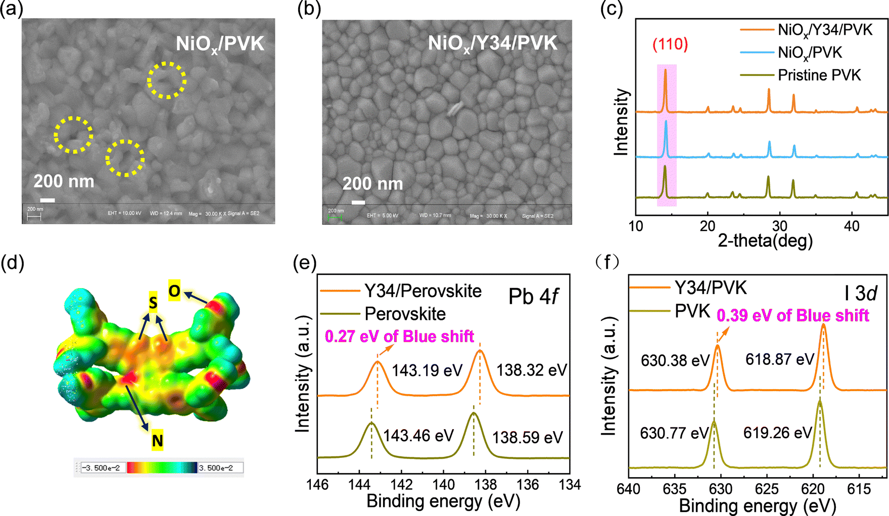 | ||
| Fig. 4 Top-view SEM images of PVK coated on (a) pristine NiOx and (b) NiOx/Y34 substrates. (c) XRD patterns of PVK. (d) ESP map. XPS spectra of Pb 4f peaks (e) and I 3d peaks (f). Here PVK refers to the perovskite film. | ||
To explore the relationship between Y34 modification and the improvement of perovskite crystal quality in depth, we conducted density functional theory (DFT) calculations. Fig. 4d shows the surface electrostatic potential (ESP) map, where the N, S, and O heteroatoms in Y34 are electron-rich groups that can act as Lewis bases to effectively bind the uncoordinated Pb2+ at the perovskite interface. In addition, we performed X-ray photoelectron spectroscopy (XPS) tests on the perovskite. In Fig. 4e, the binding energies at 143.46 eV and 138.59 eV correspond to the characteristic peaks of the Pb 4f5/2 and Pb 4f7/2 orbits of the perovskite, respectively; after Y34 modification, these two characteristic peaks shift to 143.19 eV and 138.32 eV. After the Y34 modification, the Pb 4f orbitals shift toward the low binding energy direction by 0.27 eV. Meanwhile, the characteristic peaks for I 3d orbits are shifted to lower binding energies by 0.39 eV (Fig. 4f), owing to the concomitant effect of the Pb–I bond when coordinating Pb2+ with Y34.8,28 These results reveal the interaction between the uncoordinated Pb2+ in the perovskite and the electronegative heteroatoms, such as N, S, and O, in the Y34 molecule, which enhances the crystallinity of the perovskite (Fig. 4b).
To assess the trap densities at the interface between perovskite and HTM layers, we carried out a space charge-limited current (SCLC) test. We fabricated hole-only devices with a configuration of ITO/HTMs/perovskite/spiro-OMeTAD/Ag. As depicted in Fig. S5 (ESI†), by fitting the SCLC region of the curves, the trap-filled limit voltage (VTFL) values corresponding to the turning point between the Ohmic region and trap-filling region of the curves are determined to be 0.70 V for the device with pristine NiOx and 0.56 V for the device configured with NiOx/Y34. Moreover, the corresponding trap-state density (Nt) data of the devices are calculated as 2.11 × 1016 cm−2 and 1.75 × 1016 cm−2, respectively. A lower Nt can suppress the defect-assisted non-radiative recombination in the device based on Y34-modified NiOx, favoring enhanced VOC and FF.
3.3 Work stability and long-term device stability test
To assess the reliability of PSCs, we measured the stable output power at the maximum power point (MPP) for 300 s under continuous illumination, as shown in Fig. 5a. The device based on pristine NiOx HTL exhibits a stable photocurrent of 21.77 mA cm−2 and a PCE of 17.5% at a bias of 0.80 V, while the NiOx/Y34-based device demonstrates a stable photocurrent of 22.13 mA cm−2 and a PCE of 18.35% at a bias of 0.83 V, which is in good agreement with the J–V characteristics. In addition, we also evaluated long-term device stability under one-sun irradiation under a N2 environment at room temperature. As shown in Fig. 5b, the device based on NiOx sustained 64% of its initial efficiency after aging for 90 days. In contrast, the iPSC with NiOx/Y34 retained 76% of its initial efficiency under the same conditions. | ||
| Fig. 5 (a) The stabilized photocurrent density and PCE of PSCs with NiOx and NiOx/Y34 operated at their maximum power points. (b) Long-term stability of PSCs stored in a N2-filled glove box. (c) Ni 2p XPS spectra of NiOx before and after Y34 modification. (d) The contents of Ni species in NiOx and NiOx/Y34 films. | ||
The incorporation of multiple heteroatoms (O, N, S) in Y34 caused an effective passivation effect on uncoordinated Pb2+ in perovskite, which enhanced the crystallization quality of perovskite, thereby improving the device stability. In addition, the detrimental Ni>3+ species on the surface of NiOx critically impacted the perovskite films and device stability. Therefore, XPS measurements were performed to access the redox behavior of NiOx with Y34 by probing the electronic state of the Ni element in different substrates. As shown in Fig. 5c, the binding energies of Ni 2p displayed two typical peaks at 853.73 and 856.04 eV for pristine NiOx, while peaks at 853.93 and 856.24 eV were present for the NiOx/Y34 film. These two typical peaks are attributed to the Ni2+ and Ni3+ species, respectively.20,33 In addition, a shift to a higher binding energy by 0.20 eV was detected following the incorporation of Y34. We reason that this shift is attributed to the interaction between Ni and heteroatoms (O, N, S) within Y34. We further integrated the peak areas of the Ni 2p states to calculate the ratios of Ni3+/Ni2+, which were determined to be 0.93 for pristine NiOx and 1.27 for NiOx/Y34 (Fig. 5d). In comparison to that of pristine NiOx, the slightly elevated ratio of Ni3+/Ni2+ for NiOx/Y34 indicated an enhancement of p-type characteristics in NiOx films when covered with Y34.34,35 Moreover, detrimental Ni>3+ species decreased on the surface of the NiOx/Y34 substrate. This result can be ascribed to the fact that the interfacial layer of the Y34 molecule offers Lewis base sites (O, N, S) to reduce the excessive number of Ni>3+ sites in NiOx film, which can further suppress the potential redox reactions between the Ni>3+ of NiOx and the iodide species of the perovskite layers.20,36 As a result, the device stability of NiOx-based inverted PSCs is achieved.
4. Conclusions
In summary, a novel semiconductor, Y34, with a butterfly-like structure was designed and synthesized by incorporating four MeO-TPA electron donors with π-conjugated dithieno[3,2-a:2′,3′-c]phenazine core. Incorporating Y34 as a modification layer on the NiOx surface effectively regulates the energy level with the perovskite layer and enhances hole extraction/transfer to achieve an efficiency of 18.79% with negligible hysteresis. Additionally, Y34 can effectively improve the quality of perovskite film and reduce the concentration of harmful Ni>3+ species on the surface of NiOx, thereby enhancing long-term device stability. iPSC retains 76% of its original efficiency after 90 days of one-sun irradiation in the N2 environment. These results suggest that an organic semiconductor with a butterfly structure is a promising alternative for the development of efficient and stable inverted PSCs.Data availability
The data supporting this article have been included as part of the ESI.†Conflicts of interest
The authors declare no competing financial interests.Acknowledgements
This work was supported by the National Natural Science Foundation of China (62204093 and 22005218) and the Open Project Fund of the National & Local Joint Engineering Research Center for Deep Utilization Technology of Rock-salt Resource (SF202201). The authors would like to thank Hui Wang for his help in SEM testing.Notes and references
- J. Park, J. Kim, H.-S. Yun, M. J. Paik, E. Noh, H. J. Mun, M. G. Kim, T. J. Shin and S. I. Seok, Nature, 2023, 616, 724–730 CrossRef CAS PubMed.
- J. Suo, B. Yang, E. Mosconi, D. Bogachuk, T. A. S. Doherty, K. Frohna, D. J. Kubicki, F. Fu, Y. Kim, O. Er-Raji, T. Zhang, L. Baldinelli, L. Wagner, A. N. Tiwari, F. Gao, A. Hinsch, S. D. Stranks, F. De Angelis and A. Hagfeldt, Nat. Energy, 2024, 9, 172–183 CrossRef CAS.
- M. Kim, J. Jeong, H. Lu, T. K. Lee, F. T. Eickemeyer, Y. Liu, I. W. Choi, S. J. Choi, Y. Jo, H.-B. Kim, S.-I. Mo, Y.-K. Kim, H. Lee, N. G. An, S. Cho, W. R. Tress, S. M. Zakeeruddin, A. Hagfeldt, J. Y. Kim, M. Gratzel and K. D. Suk, Science, 2022, 375, 302–306 CrossRef CAS PubMed.
- M. Li, B. Jiao, Y. Peng, J. Zhou, L. Tan, N. Ren, Y. Ye, Y. Liu, Y. Yang, Y. Chen, L. Ding and C. Yi, Adv. Mater., 2024, 2406532, DOI:10.1002/adma.202406532.
- Q. Tan, Z. Li, G. Luo, X. Zhang, B. Che, G. Chen, H. Gao, D. He, G. Ma, J. Wang, J. Xiu, H. Yi, T. Chen and Z. He, Nature, 2023, 620, 545–551 CrossRef CAS.
- H. Zhang and N.-G. Park, eScience, 2022, 2, 567–572 CrossRef.
- C. Liu, Y. Yang, H. Chen, J. Xu, A. Liu, A. S. R. Bati, H. Zhu, L. Grater, S. S. Hadke, C. Huang, V. K. Sangwan, T. Cai, D. Shin, L. X. Chen, M. C. Hersam, C. A. Mirkin, B. Chen, M. G. Kanatzidis and E. H. Sargent, Science, 2023, 382, 810–815 Search PubMed.
- B. Niu, H. Liu, Y. Huang, E. Gu, M. Yan, Z. Shen, K. Yan, B. Yan, J. Yao, Y. Fang, H. Chen and C. Z. Li, Adv. Mater., 2023, 35, 2212258 CrossRef CAS.
- Y. Hou, W. Chen, D. Baran, T. Stubhan, N. A. Luechinger, B. Hartmeier, M. Richter, J. Min, S. Chen, C. O. R. Quiroz, N. Li, H. Zhang, T. Heumueller, G. J. Matt, A. Osvet, K. Forberich, Z. G. Zhang, Y. Li, B. Winter, P. Schweizer, E. Spiecker and C. J. Brabec, Adv. Mater., 2016, 28, 5112–5120 CrossRef CAS.
- K. Zhao, Q. Liu, L. Yao, C. Değer, J. Shen, X. Zhang, P. Shi, Y. Tian, Y. Luo, J. Xu, J. Zhou, D. Jin, S. Wang, W. Fan, S. Zhang, S. Chu, X. Wang, L. Tian, R. Liu, L. Zhang, I. Yavuz, H.-F. Wang, D. Yang, R. Wang and J. Xue, Nature, 2024, 632, 301–306 CrossRef CAS.
- C. Zhang, X. Shen, M. Chen, Y. Zhao, X. Lin, Z. Qin, Y. Wang and L. Han, Adv. Energy Mater., 2022, 13, 2203250 CrossRef.
- W. Chen, F. Z. Liu, X. Y. Feng, A. B. Djurišić, W. K. Chan and Z. B. He, Adv. Energy Mater., 2017, 7, 1700722 CrossRef.
- H. Zhang, C. Zhao, J. Yao and W. C. H. Choy, Angew. Chem., Int. Ed., 2023, 62, e202219307 CrossRef CAS PubMed.
- S. Park, D. W. Kim and S. Y. Park, Adv. Funct. Mater., 2022, 32, 2200437 CrossRef CAS.
- Z. Li, B. H. Jo, S. J. Hwang, T. H. Kim, S. Somasundaram, E. Kamaraj, J. Bang, T. K. Ahn, S. Park and H. J. Park, Adv. Sci., 2019, 6, 1802163 Search PubMed.
- H. Wang, Z. Qin, X. Li, C. Zhao and C. Liang, Energy Environ. Mater., 2023, 7, e12666 CrossRef.
- X. Wang, J. Jiang, Z. Liu, A. Li, T. Miyasaka and X. F. Wang, Small, 2024, 20, 2400356 CrossRef CAS.
- Y. Zhou, X. Huang, J. Zhang, L. Zhang, H. Wu, Y. Zhou, Y. Wang, Y. Wang, W. Fu and H. Chen, Adv. Energy Mater., 2024, 14, 2400616 CrossRef CAS.
- R. Xu, X. Xu, R. Luo, Y. Li, G. Wang, T. Liu, N. Cai and S. Yang, J. Energy Chem., 2022, 67, 797–804 CrossRef CAS.
- R. Ramanujam, H. L. Hsu, Z. E. Shi, C. Y. Lung, C. H. Lee, G. Z. Wubie, C. P. Chen and S. S. Sun, Small, 2024, 20, 2310939 CrossRef CAS.
- R. Das Adhikari, H. Baishya, M. J. Patel, D. Yadav and P. K. Iyer, Small, 2024, 2404588, DOI:10.1002/smll.202404588.
- C. Tian, A. Sun, R. Zhuang, Y. Zheng, X. Wu, B. Ouyang, J. Du, Z. Li, X. Wu, J. Chen, J. Cai, Y. Hua and C. C. Chen, Adv. Mater., 2024, 36, 2404797 Search PubMed.
- X. Sun, C. Zhang, D. Gao, S. Zhang, B. Li, J. Gong, S. Li, S. Xiao, Z. Zhu and Z. A. Li, Adv. Funct. Mater., 2024, 34, 2315157 CrossRef CAS.
- L. Li, X. Zhang, H. Zeng, X. Zheng, Y. Zhao, L. Luo, F. Liu and X. Li, Chem. Eng. J., 2022, 443, 136405 CrossRef CAS.
- H. Wang, W. Zhang, B. Wang, Z. Yan, C. Chen, Y. Hua, T. Wu, L. Wang, H. Xu and M. Cheng, Nano Energy, 2023, 111, 108363 CrossRef CAS.
- M. Liu, L. Bi, W. Jiang, Z. Zeng, S.-W. Tsang, F. R. Lin and A. K. Y. Jen, Adv. Mater., 2023, 35, 2304415 Search PubMed.
- Z. Wang, C. Xu, Z. Yang, Y. Zou, K. Zhang, P. Gao, W. Xu, G. Li, J. Chen and M. Liang, Dyes Pigm., 2023, 211, 111066 Search PubMed.
- T. Wang, Z. Wang, Z. Ma, J. Kang, Z. Wang, X. Zong and S. Xue, Chem. Eng. J., 2024, 496, 154011 Search PubMed.
- X. Zhang, W. Qiu, S. Apergi, S. Singh, P. Marchezi, W. Song, C. Sternemann, K. Elkhouly, D. Zhang, A. Aguirre, T. Merckx, A. Krishna, Y. Shi, A. Bracesco, C. van Helvoirt, F. Bens, V. Zardetto, J. D’Haen, A. Yu, G. Brocks, T. Aernouts, E. Moons, S. Tao, Y. Zhan, Y. Kuang and J. Poortmans, ACS Energy Lett., 2023, 8, 2532–2542 CrossRef CAS.
- X. Sun, Z. Li, X. Yu, X. Wu, C. Zhong, D. Liu, D. Lei, A. K. Y. Jen, Z. A. Li and Z. Zhu, Angew. Chem., Int. Ed., 2021, 60, 7227–7233 CrossRef CAS.
- T. Cui, X. Zong, Y. Wang, L. Duan, M. Li, Z. Sun and S. Xue, J. Power Sources, 2019, 435, 226817 CrossRef CAS.
- Y. Cheng, Q. Fu, X. Zong, Y. Dong, W. Zhang, Q. Wu, M. Liang, Z. Sun, Y. Liu and S. Xue, Chem. Eng. J., 2021, 421, 129823 CrossRef CAS.
- S. Ko, T. Yong, S.-K. Kim, J. Y. Park, G. Lee, H. R. You, S. Han, D. H. Lee, S. Choi, Y. C. Choi, Y. Kim, N.-S. Lee, S. Song and J. Choi, Solar RRL, 2023, 7, 2300049 CrossRef CAS.
- B. Parida, S. Yoon, J. Ryu, S. Hayase, S. M. Jeong and D.-W. Kang, ACS Appl. Mater. Interfaces, 2020, 12, 22958–22970 CrossRef CAS.
- A. Yi, S. Chae, H. Lee, S. H. Lee, D. H. Kim and H. J. Kim, Solar RRL, 2021, 5, 2100243 CrossRef CAS.
- C. C. Boyd, R. C. Shallcross, T. Moot, R. Kerner, L. Bertoluzzi, A. Onno, S. Kavadiya, C. Chosy, E. J. Wolf, J. Werner, J. A. Raiford, C. de Paula, A. F. Palmstrom, Z. J. Yu, J. J. Berry, S. F. Bent, Z. C. Holman, J. M. Luther, E. L. Ratcliff, N. R. Armstrong and M. D. McGehee, Joule, 2020, 4, 1759–1775 CrossRef CAS.
Footnote |
| † Electronic supplementary information (ESI) available. See DOI: https://doi.org/10.1039/d4nj04426f |
| This journal is © The Royal Society of Chemistry and the Centre National de la Recherche Scientifique 2025 |