
Spiking frequency adaptability and multi-weight synergy in artificial neuronal modules via bifunctional NbOx memristors†
Shuai-Ming
Chen
a,
Li-Chung
Shih
 a,
Jing-Ci
Gao
a,
Song-Xian
You
a,
Kuan-Ting
Chen
a,
Pei-Lin
Lin
a,
Kai-Shin
Hsu
a,
Chi-Chien
Chen
a,
Wei-Lun
Chen
a and
Jen-Sue
Chen
*ab
a,
Jing-Ci
Gao
a,
Song-Xian
You
a,
Kuan-Ting
Chen
a,
Pei-Lin
Lin
a,
Kai-Shin
Hsu
a,
Chi-Chien
Chen
a,
Wei-Lun
Chen
a and
Jen-Sue
Chen
*ab
aDepartment of Materials Science and Engineering, National Cheng Kung University, Tainan 70101, Taiwan. E-mail: jenschen@ncku.edu.tw
bProgram on Semiconductor Packaging and Testing, Academy of Innovative Semiconductor and Sustainable Manufacturing, National Cheng Kung University, Tainan 70101, Taiwan
First published on 26th June 2025
Abstract
To address the limitations of current artificial neurons in neuromorphic hardware implementation, NbOx-based bifunctional memristors are fabricated to construct oscillatory units and advanced neuronal modules. NbOx-based memristors operate as either threshold-switching memristors (TSMs) or dynamic memristors (DyMs), depending on whether electroforming is applied. TSMs are employed to build oscillatory units and further reconfigured into a weighted multi-terminal neuronal module, enabling real-time spatiotemporal summation of input spikes based on the leaky integrate-and-fire model. This module demonstrated the capability to perform spike summation and multi-weight synergy. Leveraging the gradual resistance change characteristic of DyMs, a sequential encoder is implemented, allowing the system to recognize and respond to the temporal order of spiking signals. Additionally, a DyM is integrated into the oscillatory unit to construct intensification and attenuation neurons, enabling short-term spiking frequency adaptation. The versatile spiking performance of our NbOx bifunctional memristor provides a strategic foundation for developing artificial neurons for next-generation bio-inspired spiking neural networks.
New conceptsIn this study, bifunctional NbOx-based memristors are demonstrated, leveraging both dynamic and threshold switching characteristics to develop inventive bio-realistic neuronal modules with spike summation, sequencing and frequency adaptation for neuromorphic hardware architecture. A weighted multi-terminal artificial neuronal module is implemented using threshold-switching NbOx memristors, effectively replicating multi-weight synergy and real-time spatiotemporal summation. This module aligns with the leaky integrate-and-fire model, improving neuromorphic processing capabilities. Furthermore, the integration of threshold-switching and dynamic NbOx memristors enables spiking sequence recognition and spiking frequency adaptation, allowing the spiking frequency to be modulated between 2000 Hz and inactivity. This work presents a novel methodological advancement in the emulation of neuronal functionalities, representing a significant step toward the progression of bio-inspired neuromorphic computing. |
1. Introduction
In the human nervous system, billions of neurons interact to transmit signals, enabling biological functions and eliciting appropriate responses to environmental stimuli.1,2 Neuromorphic computing, inspired by the structure and dynamics of biological neural systems, has emerged as a promising approach in artificial intelligence (AI) research, aiming to achieve energy-efficient and brain-like information processing.3–6 To enhance the performance of neuromorphic systems, researchers have investigated key neuronal characteristics such as synaptic plasticity, optical responsiveness, and intrinsic excitability.7–25 These features have shown strong potential for enabling advanced AI capabilities, including image recognition, pattern classification, human–machine interaction, and sensor-integrated robotics.26 Such developments demonstrate the versatility of memristor-based neural devices in mimicking both synaptic transmission and neuronal spiking behaviors.Spiking neural networks (SNNs), which more closely emulate the temporal dynamics of biological neurons, offer several advantages—enhanced computational efficiency, real-time responsiveness, and low power consumption—particularly in neuromorphic applications.1–8,12,17,27–29 Although the theoretical foundation of SNNs is well established, practical deployment in neuromorphic computing demands efficient and scalable hardware implementations. Conventional CMOS-based neuromorphic circuits, which require complex architectures and numerous transistors per neuron, face limitations in terms of scalability and energy efficiency for large-scale networks. In contrast, memristor-based devices present a compact and energy-efficient alternative by leveraging intrinsic switching mechanisms to replicate core neuronal functions.7–19 Among these, volatile threshold switching memristors (TSMs) have shown exceptional promise for hardware-based neuron implementation, enabling highly compact and efficient spike-based computation.7,8,10,11,21,30–40
A Pearson–Anson-like relaxation oscillator constructed with TSMs serves as a simple spike generator, functioning as a hardware-based oscillatory unit in SNNs.7–9,21,27,32,35,37,39,41 TSM-based oscillatory units have demonstrated their capability to serve as encoders or leaky integrate-and-fire (LIF) models in several studies.7–10 The stable threshold switching behavior observed in transition-metal oxides, such as VOx8,15,31,37,40 and NbOx,9,21,27,32,35,39,41 arises from their S-type negative differential resistance (NDR), which results from thermally induced positive feedback mechanisms. These mechanisms include Joule heating and Poole–Frenkel conduction and, in many cases, are accompanied or even dominated by electronic phase transitions, such as the Mott transition, which involves a thermally driven metal–insulator transition without permanent structural changes.30,42 NbOx has been reported to exhibit relatively better thermal stability than VOx, making it a suitable choice for the active layer in this work.43 To further enhance the intrinsic computational capabilities of SNNs at the hardware level, additional features—such as multi-terminal connectivity and adaptability—represent promising directions for development.
Fig. 1a illustrates a multipolar biological neuron and an artificial neuronal module inspired by its functionality. Multipolar neurons represent a predominant neuron type, especially prevalent within the cerebral cortex. These neurons, characterized by a single axon and multiple dendrites, receive and integrate signals from numerous presynaptic neurons. In SNNs, neural connections are inspired by these multipolar neurons. Network computation is realized through interactions between neurons, where their collective activity enables the processing of complex signals and the execution of network-level computations.3,4,27 When combined with synaptic weights for each connection, a multi-terminal neuronal module performs computations on all incoming signals, achieving spatiotemporal summation at the hardware level to process and integrate inputs over time.1,2 This configuration allows for direct spatiotemporal summation through the circuit's intrinsic physical mechanisms, enabling efficient signal integration and processing without additional computational overhead.
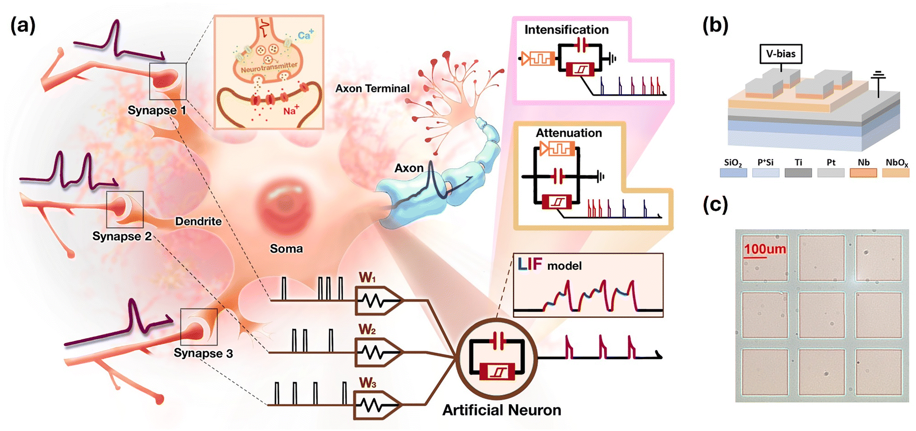 | ||
| Fig. 1 (a) A schematic illustration of an artificial neuron and its functionalities, highlighting its analogy to a multipolar biological neuron. The artificial neuron model integrates multiple inputs based on the weight of each connection and the timing of input signals, enabling spatiotemporal summation and weight synergy. The DyM further enhances the functionality of oscillatory units by enabling spiking intensification and attenuation, while also providing adaptability. (b) Schematic diagram of the Pt/Nb(O)/NbOx/Pt device structure. (c) Optical microscopy top-view image of the fabricated Pt/Nb(O)/NbOx/Pt device. | ||
Beyond spatiotemporal summation, biological neurons exhibit adaptability by dynamically adjusting their firing rates in response to stimuli.44–48 This adaptability is crucial for efficient neural computation, allowing neurons to regulate their responses based on input intensity and temporal patterns.46–48 By modulating spiking frequency, neurons control information flow, preventing excessive activity that could lead to energy inefficiency or signal distortion—an effect linked to synaptic depression.45 Conversely, synaptic facilitation enhances signal transmission by temporarily increasing synaptic strength, preventing signal saturation, and ensuring neurons do not fire continuously at maximum rates, which could otherwise impair information encoding.44 Such dynamic regulation is particularly important for tasks involving temporal coding and sequence processing, as it enables neural networks to adjust sensitivity to changing input dynamics, improving computational efficiency and information retention.6,28,46–48
To achieve spiking frequency adaptation at the hardware level, we integrate a dynamic memristor (DyM) into the oscillatory unit, configuring it as the intensification neuron and the attenuation neuron. The DyM, characterized by gradual switching behavior,34,36,49–52 allows the oscillatory unit to modulate its spiking response in real-time. This integration enables the circuit to optimize information processing dynamically while maintaining efficient resource utilization, advancing neuromorphic computing with enhanced adaptability.
In this work, bifunctional NbOx-based memristors, capable of exhibiting both DyM and TSM behaviors, are fabricated and integrated into neuromorphic circuits. NbOx-based TSMs are utilized to construct a weighted artificial neuronal module, enabling spatiotemporal summation through weighted integration and synergistic processing of randomly timed spike stimuli from three distinct inputs. Additionally, by leveraging the interaction between resistors and DyMs, the modified oscillatory unit functions as a sequential encoder, distinguishing the temporal order of pulse arrivals at two terminals and generating a corresponding response based on the input sequence. Furthermore, by configuring the system into an intensification neuron and an attenuation neuron, the circuit successfully emulates neural spike adaptability. This work presents a multifunctional hardware-level artificial neuron, advancing bio-inspired neuromorphic computing and paving the way for more resilient, scalable, and adaptive AI systems.
2. Results and discussion
2.1. Materials characterization
Devices with a Pt/Nb(O)/NbOx/Pt multilayer structure are fabricated and analyzed. Fig. 1b shows a schematic diagram of the device stack. An optical microscopy image of the fabricated devices is shown in Fig. 1c, where each square represents a single cell with an area of 200 × 200 μm2. The TEM image in Fig. 2a presents a detailed cross-sectional view, showing a 40 nm thick NbOx layer, a 16 nm thick Nb(O) layer, a 77 nm thick Pt top electrode, and an 89 nm thick Pt bottom electrode. Fig. 2b shows the selected areas for nano-beam electron diffraction (NBED) analysis within the Nb(O) and NbOx layers, as marked by the red circles labeled 1 and 2, respectively. The corresponding NBED patterns are shown in Fig. 2c and d. The diffraction pattern from region 1 (Fig. 2c) suggests that the Nb(O) layer is polycrystalline, while the pattern from region 2 (Fig. 2d) reveals that the NbOx layer is amorphous. Fig. 2e and f present the Nb 3d X-ray photoelectron spectroscopy (XPS) spectra for the Nb(O) and NbOx layers, respectively. The spectra exhibit five distinct peaks at binding energies of approximately 202.3, 203.4, 204.1, 205.6, and 207.4 eV, corresponding to Nb metal, NbO, NbOδ (1 < δ < 2), NbO2, and Nb2O5.53,54 The relative area percentages of these oxidation states are shown in the legends to the right of each figure. Notably, despite the Nb(O) layer being deposited via sputtering using a Nb metal target in an Ar atmosphere, the NbO component still accounts for a significant 48.6% of the total composition. Fig. 2g shows the HAADF-STEM image of the TSM, highlighting the distinct Nb(O) and NbOx layers in the structure. The corresponding EDS mapping images for Nb, Pt, and O are presented in Fig. 2h–j, respectively, depicting the elemental distribution across the TSM layers. Notably, the presence of oxygen within the Nb(O) layer, as indicated by the O signal mapping in Fig. 2j, is consistent with the XPS analysis, which confirms the significant presence of NbO bonding in this region. This correlation further supports the formation of NbO within the Nb(O) layer.41 The energy band structure of the NbOx layer was investigated using ultraviolet photoelectron spectroscopy (UPS) and UV–Vis spectroscopy. Fig. S1a (ESI†) presents the full-range UPS spectrum of the NbOx layer, acquired using a He I photon source (hν = 21.2 eV). Two regions of interest were selected for detailed analysis: the secondary electron cutoff and the valence band edge. As shown in Fig. S1b (ESI†), the secondary electron cutoff is located at 16.9 eV, while the valence band edge, identified in Fig. S1c (ESI†), indicates that the Fermi level is positioned at 3.46 eV above the valence band maximum (EV). Fig. S1d (ESI†) shows the UV-Vis transmittance spectrum, and the corresponding Tauc plot in Fig. S1e (ESI†) reveals an optical bandgap (Eg) of 3.67 eV. These electronic properties are summarized in the energy band diagram shown in Fig. S1f (ESI†). For reference, the work functions of Nb and Pt are 4.3 eV and 5.65 eV, respectively.55 | ||
| Fig. 2 (a) TEM image of the Pt/Nb(O)/NbOx/Pt device, showing the layered structure with a 77 nm Pt top electrode (TE), 16 nm Nb(O) layer, 40 nm NbOx layer, 89 nm Pt bottom electrode (BE), 15 nm Ti adhesion layer, and 102 nm SiO2 substrate. (b) TEM image of the Pt/Nb(O)/NbOx/Pt device, with red circles indicating the selected areas for NBED analysis. (c) NBED pattern of the Nb(O) layer, suggesting the presence of a polycrystalline structure. (d) NBED pattern of the NbOx layer, indicating an amorphous structure. (e) X-ray photoelectron spectroscopy (XPS) spectra of the Nb 3d core level in the Nb(O) layer. (f) XPS spectra of the Nb 3d core level in the NbOx layer. (g) HAADF-STEM image of the Pt/Nb(O)/NbOx/Pt device. (h)–(j) EDS mapping of (h) Nb, (i) Pt, and (j) O, illustrating the elemental distribution across the device structure. | ||
2.2. Resistive switching behavior: dynamic memristor and threshold switching memristor
To construct functional units for neuromorphic hardware, it is essential to develop simple oscillatory units capable of generating spike signals. Additionally, incorporating adaptive functionality into these units requires the integration of components with gradual switching characteristics to facilitate dynamic modulation. The Pt/Nb(O)/NbOx/Pt device is capable of exhibiting two distinct electrical characteristics. The device initially exhibits DyM behavior (Fig. 3a). After electroforming with a 0 V → 8 V → 0 V sweep (Fig. 3b), it transitions to a volatile TS characteristic (Fig. 3c). | ||
| Fig. 3 (a) Initial I–V characteristics of the Pt/Nb(O)/NbOx/Pt device under a voltage sweep from 3 V to −3 V and back to 3 V, demonstrating the DyM behavior before electroforming. (b) Electroforming process with a voltage sweep from 0 V to 8 V and back to 0 V. (c) After electroforming, the Pt/Nb(O)/NbOx/Pt device exhibits TS behavior. (d) Schematic representation of the conduction and recovery mechanisms in the DyM, illustrating oxygen vacancy migration and diffusion. (e) Formation of the conductive filament and TS region during the electroforming process. Oxygen vacancies aggregate into a filament, while a TS region forms within the Nb(O) layer. Upon voltage removal, the filament remains in the NbOx layer, and the TS region returns to a HRS. (f) Schematic of the conduction states in the Pt/Nb(O)/NbOx/Pt device during TS operation, showing the transition between high- and low-resistance states. | ||
Fig. 3a shows the I–V characteristic of the DyM, measured by applying a voltage sweep of 3 V → −3 V → 3 V to the Pt/Nb(O)/NbOx/Pt device, revealing a hysteresis window in the negative bias region. The reverse sweep (−3 V to 0 V) shows higher current than the forward sweep, indicating a history-dependent conductance. Notably, during the 3 V → −3 V sweep, a current “overshoot” is observed near 0.75 V, as marked by the red dot in Fig. S2a (ESI†), where the current drops to approximately 10−11 A. To better clarify this phenomenon, a linear-scale plot (Fig. S2b, ESI†) and an enlarged view (Fig. S2c, ESI†) are provided. The red dot indicates the moment when the current passes through 0 A during the 3 V → −3 V sweep. In addition, the blue dot in Fig. S2a and c (ESI†) marks the zero-crossing point during the −3 V → 3 V sweep. This non-zero-crossing behavior is attributed to parasitic capacitance inherent in the MIM (metal–insulator–metal) structure. The electrical characteristics of the memristor, when coupled with parasitic capacitance, results in the non-zero-crossing I–V characteristics.56
To further understand the underlying conduction mechanism, Fig. 3d illustrates the oxygen vacancy transport and recovery processes within the DyM device. Initially, oxygen vacancies are uniformly distributed within the NbOx layer. Under a positive bias applied to the top electrode, the Schottky barrier at the Pt/NbOx interface limits the current flow, restricting electron injection.34,36,49,52 Conversely, when a negative bias is applied, the electric field drives oxygen vacancies toward the Nb(O) layer side, leading to an accumulation of oxygen vacancies near the Nb(O)/NbOx interface (step 1 in Fig. 3d). This accumulation modulates the local conductivity, facilitating electron transport and resulting in an increase in current. Upon the removal of the applied voltage, oxygen vacancies gradually diffuse back to their original distribution due to the concentration gradient, restoring the device to its initial state. To examine the role of interface effects,57 a control device with the structure Pt/NbOx/Pt was fabricated for comparison with the original Pt/Nb(O)/NbOx/Pt configuration. Fig. S3a (ESI†) shows that the Pt/Nb(O)/NbOx/Pt device exhibits asymmetric current responses under opposite bias polarities. This asymmetry is attributed to the lower energy barrier at the Nb(O)/NbOx interface, as illustrated in the energy band diagram (Fig. S3b, ESI†). In contrast, the Pt/NbOx/Pt control device (Fig. S3c, ESI†) displays a more symmetric I–V response, consistent with the presence of symmetric barriers at both Pt/NbOx interfaces, as shown in Fig. S3d (ESI†). These observations indicate that the electrode/NbOx interface plays a significant role in shaping the device's electrical characteristics.
The Pt/Nb(O)/NbOx/Pt device undergoes an electroforming process to enable TS behavior, as shown in Fig. 3b. Fig. 3e illustrates the formation of a conductive filament and the development of a TS region during the electroforming process. Initially, oxygen vacancies are uniformly distributed within the NbOx layer. As a high forming voltage is applied, these oxygen vacancies migrate and aggregate, forming a conductive filament within NbOx while simultaneously inducing a TS region within the Nb(O) layer (step 1 and step 2 in Fig. 3e). The TS region is assumed to form at the top of the filament, which is created by oxygen migration from the NbOx layer to the Nb(O) layer.30,42 Additionally, the heat generated during the electroforming process further facilitates this migration. Upon removal of the applied bias, the filament is retained in the NbOx layer, whereas the TS region transitions back to a high-resistance state (HRS), marking the completion of the forming process (step 3 in Fig. 3e).
Fig. 3c presents the TSM characteristics of the Pt/Nb(O)/NbOx/Pt device after the electroforming process, with the representative I–V curve measured under a compliance current (CC) of 10 mA using a voltage sweep of 0 V → 2 V → 0 V. The TSM device remains in a high resistance state (HRS) when the applied voltage is below the threshold voltage (Vth). Upon reaching Vth, the device transitions to a low resistance state (LRS). During the reverse voltage sweep from 2 V to 0 V, the TSM reverts to its HRS once the applied voltage drops below hold voltage (Vhold), demonstrating TS behavior. The Vth is approximately 1.8 V, while the Vhold is around 1.5 V. Fig. 3f illustrates the conductive behavior of the Pt/Nb(O)/NbOx/Pt device during voltage sweeping. Since the conductive filament has already been established, the electric field generated by the applied voltage directly influences the TS region. (step 1 in Fig. 3f). When the applied voltage exceeds Vth, the temperature of the TS region increases due to Joule heating, which in turn lowers its resistance through the Poole–Frenkel conduction mechanism. In addition to this thermally assisted conduction process, it is also possible that a localized electronic phase transition—such as a thermally triggered Mott transition—occurs in the NbOx matrix. This transition, which involves a reversible metal–insulator transition driven by strong electron correlation effects, may further contribute to the abrupt resistance change observed during threshold switching.30,42 As the resistance decreases, the resulting higher current generates additional heat, further reducing the resistance and reinforcing a positive feedback loop that drives the transition to the LRS (step 2 in Fig. 3f). Once the voltage drops below Vhold, the TSM reverts to the HRS (step 3 in Fig. 3f). The electrical behavior during the electroforming process was analyzed to identify potential conduction mechanisms (Fig. S4a, ESI†).58 The curve was divided into four distinct regions (regions 1–4) for fitting analysis. Region 1 (Fig. S4b, ESI†): a linear relationship is observed in the ln(I) vs. ln(V) plot, with a slope of approximately 0.97, indicating Ohmic conduction. Region 2 (Fig. S4c, ESI†): a linear fitting in the ln(I) vs. V1/2 plot suggests the presence of Schottky emission, possibly originating from the energy barrier at the Pt/NbOx bottom electrode interface. Region 3 (Fig. S4d, ESI†): a steep slope of ∼8.08 in the ln(I) vs. ln(V) plot may reflect the onset of a trap-filled limit regime, consistent with the space-charge-limited current (SCLC) model. Region 4 (Fig. S4e, ESI,† reverse sweep after forming): a linear ln(I) vs. ln(V) relationship with a slope of ∼1.1 is observed. Fig. S5 and S6 (ESI†) presents 50 voltage sweep cycles for each of the 20 devices for the DyM and TSM, respectively, illustrating the cycle-to-cycle and device-to-device variations in the devices. In addition, endurance tests were conducted on the device, with the results presented in Fig. S7 (ESI†). The data demonstrate stable performance over multiple cycles and devices.
2.3. Multi-dendrite driven spike summation and weight synergy
To generate spike signals, the TSM device can be utilized as a key component in constructing a Pearson–Anson-like relaxation oscillator, serving as an oscillatory unit. As shown in Fig. 4a, the oscillatory unit consists of a source voltage (Vin), a load resistor (RL), a capacitor (C), and a parallel resistor (RP). Vout1 and Vout2 are connected to an oscilloscope to monitor the oscillatory behavior and spike signals, respectively. The TSM-based oscillatory unit is designed to convert voltage inputs into spike signals, enabling efficient emulation of input signal encoding and computation within SNNs. Fig. 4b illustrates the oscillatory behavior and spike signals of the oscillatory unit, configured with RL = 540 Ω, RP = 33 Ω, and C = 100 nF, under an input voltage Vin of 3.25 V. The oscillation and spiking frequency are measured to be 44.6 kHz. Initially, Vin is applied to the oscillatory unit, initiating the capacitor charging process. When the voltage across the TSM exceeds Vth, the TSM undergoes resistive switching from HRS to LRS, leading to the rapid discharge of the capacitor. Once the voltage across the TSM drops below Vhold, the device transitions back from LRS to HRS, resuming the charging process. During the discharge process, a spike signal is detected at node Vout2. This spike signal is composed of the discharge current from the capacitor and the increasing current caused by the reduced resistance of the TSM. Following the first emitted spike, sustained oscillations between the upper boundary (U.B.) and lower boundary (L.B.) are observed at node Vout1. | ||
| Fig. 4 (a) Circuit diagram of the TSM-based oscillatory unit, where the TSM is connected in parallel with a capacitor and series with resistors RL and RP. (b) Measured oscillatory and spiking behavior of the TSM-based oscillatory unit with RL = 540 Ω, C = 100 nF, and Vin = 3.25 V, showing a spiking frequency of 44.6 kHz. (c) Spiking rate as a function of RL with a fixed Vin of 3.25 V and C of 100 nF. (d) Spiking rate as a function of Vin with RL fixed at 572 Ω and C fixed at 100 nF. (e) Spiking rate as a function of C with a constant Vin of 3.25 V and RL of 572 Ω. (f) Illustration of the LIF model, showing the relationship between input pulses and output spikes. The integration phase (red) accumulates input signals, while the leakage phase (blue) gradually dissipates the membrane potential. Once the threshold is reached, a spike is generated (purple), followed by a reset. (g) Summary of the required number of input pulses to generate a spike as a function of pulse interval, with Vin fixed at 3.25 V and RL at 572 Ω. | ||
The spiking rate of the oscillatory unit depends on circuit components, including the resistance of RL, the pulse amplitude of Vin, and the capacitance of C. Fig. 4c shows the relationship between RL and the spiking rate, with Vin fixed at 3.25 V and C at 100 nF. As RL increases from 158 Ω to 780 Ω, the spiking frequency decreases, indicating a negative correlation between RL and the spiking rate. This reduction occurs due to the decrease in input current caused by a larger RL, which slows the charge accumulation on the capacitor. Notably, at RL = 158 Ω, only a single spike is generated since the TSM remains in the LRS and fails to reset. In contrast, at RL = 780 Ω, no spiking occurs as the voltage across the TSM is insufficient to reach Vth. The raw data are provided in Fig. S8 (ESI†).
For the test with varying Vin, a stair-like waveform ranging from 2 V to 7 V is applied, as illustrated in Fig. S9 (ESI†). At Vin = 3.25 V, a spiking rate of 44.4 kHz is observed. As Vin increases, the spiking rate increases accordingly, as shown in Fig. 4d. With a relatively high Vin, the TSM is held in the LRS, suppressing oscillations. Conversely, when Vin is too low, the voltage across the TSM remains insufficient to reach Vth, preventing spike generation. Fig. S10 (ESI†) provides enlarged plots corresponding to each Vin value from Fig. S9 (ESI†), showing a detailed view of the spiking and oscillatory behavior. The capacitance value of the C significantly influences the spiking rate. Fig. S11 (ESI†) presents the experimental results for different capacitance values of 100 nF, 1 μF, 10 μF, and 100 μF, where the corresponding spiking rates are measured at 12 kHz, 3.7 kHz, 377 Hz, and 34 Hz, respectively. As the capacitance increases, the time constant of the circuit increases, causing the voltage accumulation process to slow down and leading to a reduction in the spiking rate. Fig. 4e plots the spiking rate as a function of C, showing that smaller capacitances yield higher spiking rates, while larger ones slow down oscillations and reduce spikes.
Beyond its oscillatory behavior, the oscillatory unit can also function as a computational neuronal module, demonstrating properties akin to the LIF model. As a commonly used neuron model in SNNs, the LIF model provides a simplified yet effective representation of neural dynamics, enabling spike-based information processing.7–10 As shown in Fig. 4f, the LIF model is defined by three fundamental processes: leakage – the membrane potential gradually decays over time due to passive conductance; integration – incoming input signals accumulate, causing the membrane potential to rise; and firing – when the membrane potential exceeds a threshold, a spike is generated, and the potential resets to its resting state.
Fig. S12 (ESI†) illustrates the dynamic response of Vout1 and Vout2 in the LIF model implemented with an oscillatory unit under pulse stimulation. The experiment involves applying a sequence of 40 consecutive input pulses (Vin = 4.5 V), each with a fixed pulse width of 10 μs and intervals of 3, 4, 5, 6, 6.5, and 7 μs. During the pulse width, the capacitor charges, causing Vout1 to rise, which corresponds to the integration phase in the LIF model. During the interval period, the capacitor discharges, leading to a decrease in Vout1, representing the leakage phase. Once Vout1 reaches the threshold voltage, the TSM device undergoes TS, generating a spike at Vout2.
Fig. 4g plots the number of pulses required to trigger a spike as a function of the pulse interval extracted from Fig. S12 (ESI†). When the interval is 3 μs, only two pulses are needed to generate a spike, whereas increasing the interval to 6.5 μs requires four pulses for spike generation. Despite the total pulse count remaining at 40, a higher pulse density results in a more concentrated distribution of spikes. The leakage property of the LIF model enables it to respond based on the timing of pulse arrivals rather than solely on the total number of pulses.
In neural network computation, synaptic weights quantify the influence of one neuron on another, defining the strength of their connections. These weights play a crucial role in determining computational outcomes. By integrating multiple RL resistors into the oscillatory unit to construct a neuronal module, signals from multiple inputs can be processed with distinct weights while preserving LIF-like behavior. Fig. 5a illustrates the integration process, where the capacitor charges when RL is set to 330 Ω, with a pre-spike of Vin = 5 V and a pulse width of 2 μs. During this process, the capacitor voltage reaches approximately 0.44 V. Fig. 5b demonstrates spatial summation, where two pre-spikes from different input terminals (Vin1 with RL = 330 Ω and Vin2 with RL = 470 Ω) are applied simultaneously. The combined input results in a higher charge accumulation, reaching 0.77 V, due to the increasing current from the parallel inputs. Spatial summation in SNNs is crucial for integrating multiple synaptic inputs, allowing neurons to collectively process information from different sources. This mechanism enhances computational efficiency by enabling weighted signal synergy, which influences neuronal firing and decision-making in neuromorphic systems.
 | ||
| Fig. 5 (a) Integration observed with a single-terminal input, where the capacitor charges up to 0.44 V. The inset shows the circuit configuration used in the test. (b) Integration observed with a two-terminal input, where the capacitor charges up to 0.71 V. The inset shows the circuit configuration used in the test. (c) Neuronal module circuit configuration used in the summation test (RL = 330 Ω, 470 Ω and 680 Ω, C = 100 nF, RP = 33 Ω). (d) A 3D representation of the cumulative integration effect for multiple input combinations from three terminals (Vin1, Vin2, and Vin3) with RL values of 330 Ω, 470 Ω, and 680 Ω. (e) Extracted peak capacitor voltage levels for various input combinations. The results demonstrate that integration is enhanced through spatial summation, while also confirming that smaller RL values correspond to higher weights, leading to greater voltage accumulation. (f) Real-time spatiotemporal summation behavior demonstrated using the circuit configuration shown in (c). Three distinct input terminals (Vin1, Vin2, and Vin3) receive pulses with a 5 V amplitude, 1 V baseline, and a 30 μs pulse width. These pulses were applied at random intervals, leading to varying degrees of temporal overlap and independent signal integration. The accumulated voltage at Vout1 reflects the weighted summation of inputs, while the threshold-triggered response at Vout2 represents the resultant spike generation. | ||
To further examine the effect of multi-weight synergy, the neuronal module shown in Fig. 5c is constructed with three distinct inputs (Vin1, Vin2, and Vin3) and the corresponding RL values of 330 Ω, 470 Ω, and 680 Ω. Fig. 5d presents the charge levels induced by different input configurations, where experiments were conducted using both single-input (Vin1, Vin2, and Vin3) and multi-input combinations (Vin1 & Vin2, Vin1 & Vin3, Vin2 & Vin3, and Vin1 & Vin2 & Vin3). Since each input is assigned a distinct RL value, these configurations inherently represent the influence of both single and multiple weighted inputs. For a single input, the RL value directly determines the capacitor's charging level, where a lower RL corresponds to a higher assigned weight. When voltage pulses are applied to multiple terminals simultaneously, the capacitor accumulates more charge due to the combined effect of the corresponding weights. Fig. 5e provides a quantitative comparison of the charge levels extracted from Fig. 5d. When voltage pulses are applied to all three terminals simultaneously, the capacitor reaches a maximum charge level of 0.87 V. Among dual-input cases, the combination of RL = 330 Ω and RL = 470 Ω results in the highest charge accumulation at 0.71 V, whereas the combination of RL = 470 Ω and RL = 680 Ω produces the lowest charge accumulation at 0.52 V.
With its weighted multi-terminal structure, the neuronal module can replicate the fundamental computational process of an SNN, where networks process information through weighted connections. To evaluate the processing capability of artificial neurons, the neuronal module shown in Fig. 5c is employed to demonstrate multi-dendrite-driven real-time spatiotemporal summation. As shown in Fig. 5f, voltage pulses (5 V with a 1 V baseline) with randomly timed inputs from three distinct terminals, each associated with a different RL value, are applied to the circuit. Each pulse has a width of 30 μs. The waveform detected at Vout1 exhibits LIF model behavior, incorporating weighted integration and spatiotemporal summation. When the voltage at Vout1 reaches the threshold, a spike is generated and recorded at Vout2. In the LIF model, after a neuron fires a spike, its membrane potential should return to its initial resting state before the next integration cycle can begin. This reset mechanism prevents residual potential from accumulating, maintaining the neuron's ability to respond to subsequent inputs effectively. However, due to the TSM's Vhold being significantly far from 0 V, Vout1 resets only to the lower boundary (L.B.) of the oscillation rather than fully returning to 0 V, as shown in Fig. S12 (ESI†). To closely emulate the reset process of the LIF model, a 1 V baseline was applied to the input terminals, ensuring that Vout1 begins integration near the reset level.
Overall, modifying each input terminal with distinct RL values effectively simulates a neuron's ability in an SNN to integrate inputs with varying weights. The multi-dendrite neuronal module leverages the circuit's inherent physical properties to perform real-time spatiotemporal summation. Additionally, adjusting the input baseline helps mitigate the typical reset limitations, aligning the behavior more closely with the expected characteristics of the LIF model. This further demonstrates that the oscillatory unit is well-suited as a hardware architecture for directly performing computations in SNN processing.
2.4. Dynamic spiking modulation: sequence recognition, intensification and attenuation
In the previous section, the oscillatory unit demonstrated its capability for real-time spatiotemporal summation and exhibited behavior consistent with the LIF model. Beyond these functions, the oscillatory unit can be further enhanced by integrating components such as DyM, leveraging its unique properties to enable more diverse functionalities. Structurally identical to the Pt/Nb(O)/NbOx/Pt device, the DyM exhibits a gradual resistance change, as verified through a pulse test. As shown in the inset of Fig. S13 (ESI†), a −3.5 V pulse with varying pulse widths, ranging from 10 ms to 50 ms, was sequentially applied to the DyM. The resulting current responses are presented in Fig. S13 (ESI†), revealing a continuous increase in current as the voltage remains applied, indicating a progressive decrease in the resistance of the DyM.Building upon the dynamically resistive switching behavior of the DyM, we construct the sequential encoder circuit shown in Fig. 6a. In this circuit, the resistor RL is set to 1 kΩ, the capacitor C is 1 μF, and the resistor RP is 33 Ω. In this configuration, separate voltage inputs are applied to the DyM and RL terminals, enabling the sequential encoder to identify the order of incoming signals. This capability allows the circuit to encode temporal information, making it well-suited for recognition tasks such as speech and gesture recognition, where sequential data is crucial for pattern interpretation.34 Since the DyM device is connected in parallel with RL, the equivalent resistance of DyM//RL gradually decreases as the stimulation duration increases. Based on the known resistance values of the DyM device at various time steps and the resistance of TSM at threshold voltage, the valid range of RL is determined to be 962–1036 Ω to ensure this sequential encoder function properly.
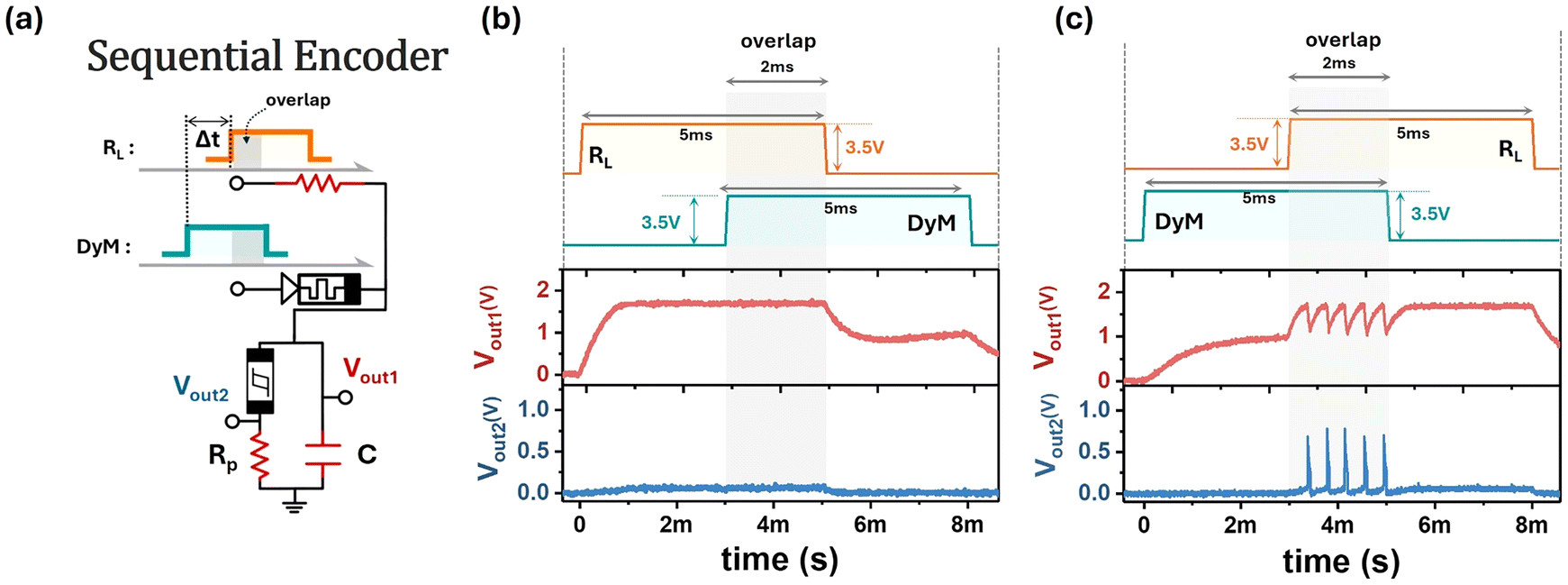 | ||
| Fig. 6 (a) Schematic of the sequential encoder, constructed with DyM and RL in parallel for sequence recognition testing. In this circuit, RL is set to 1 kΩ, the capacitor C is 1 μF, and the resistor RP is 33 Ω. (b) Sequence recognition test where the RL terminal receives the pulse first, resulting in no spike emission during the overlapping region. (c) Sequence recognition test where the DyM terminal receives the pulse first, generating spikes. | ||
Fig. 6b and c illustrate the sequence recognition experiment using the sequential encoder, where two voltage pulses (3.5 V, 5 ms width) are independently applied to the RL and DyM terminals with a slight time offset. Due to this offset, the two pulses partially overlap for a duration of 2 ms, during which both signals interact. In Fig. 6b, when the RL terminal receives the pulse first, the DyM retains relatively high resistance during the overlapping period, as its resistance has not yet sufficiently decreased to enable TS. In contrast, as shown in Fig. 6c, the DyM terminal receives the pulse earlier than the RL terminal. Due to prolonged stimulation from the input pulse, the resistance of the DyM gradually decreases over time, as demonstrated in the pulse test shown in Fig. S13 (ESI†). This reduction enables the voltage across the TSM to reach Vth during the overlapping region, thereby triggering a spike. After the stimulation ends, the DyM gradually returns to its initial state on its own, eliminating the need for external resetting and enabling continuous sequence encoding. Through the DyM's time-dependent resistive modulation, this design provides an efficient and hardware-friendly solution for encoding sequential signals in neuromorphic networks.
While the DyM enables sequential encoding in one circuit configuration, it also facilitates adaptability in another, allowing the oscillatory unit to dynamically adjust its response to input stimuli. Adaptability in neural systems is closely associated with synaptic facilitation and synaptic depression that dynamically modulate synaptic strength.44–48 Synaptic facilitation transiently enhances synaptic transmission strength when multiple action potentials reach the presynaptic terminal in rapid succession, increasing neurotransmitter release due to residual calcium.44 This residual calcium accumulates in the presynaptic terminal and facilitates the release of more neurotransmitters with subsequent action potentials, as shown in Fig. 7a. In artificial neurons, spiking intensification approximates synaptic facilitation, demonstrating an enhanced transmission of signals.
 | ||
| Fig. 7 (a) The residual calcium accumulates in the presynaptic terminal and facilitates the release of more neurotransmitters with subsequent action potentials. (b) Intensification neuron circuit configuration showing the DyM connected in parallel with RL to enhance signal transmission. (c) Intensification of spike generation under constant 3 V input with RL = 770 Ω, C = 1 μF, and RP = 33 Ω. (d) Bar chart displaying the number of spikes recorded in a ±2.5 ms window around each time point, with a progressive increase in spike count observed during the stimulation period, extracted from (c). (e) The depletion of neurotransmitter vesicles reduces synaptic transmission strength temporarily after repeated stimulation. (f) Attenuation neuron connecting the DyM in parallel with the TSM and capacitor to emulate synaptic depression. (g) The attenuation of spike generation under a constant 3 V input, with RL set to 770 Ω, C to 1 μF, and RP to 33 Ω. (h) Bar chart extracted from (g) showing the number of spikes recorded within a ±2.5 ms window, with 11 spikes at the 5 ms window and only 2 spikes remaining at the 35 ms window, illustrating the progressive decline in spike generation over time. | ||
To demonstrate spiking intensification in signal transmission, the intensification neuron is constructed by connecting the DyM in parallel with RL, both sharing the same input, as depicted in Fig. 7b. Fig. 7c presents the results of the spiking intensification experiment under a constant Vin of 3 V, with RL set to 770 Ω, C to 1 μF, and RP to 33 Ω. Initially, no spike is emitted as the DyM remains in a state of relatively high resistance. However, as the stimulus is continuously applied, the resistance of the DyM gradually decreases, lowering the equivalent resistance of the parallel DyM and RL. This reduction leads to an increase in the voltage across the TSM, eventually reaching Vth and triggering spike emission. As the resistance of the DyM continues to decrease, the capacitor's charging speed accelerates, further intensifying spike generation. Fig. 7d presents a statistical representation of spike signals recorded within a ±2.5 ms timeframe at each time point, extracted from Fig. 7c. Initially, only one spike is observed at the 5 ms mark. As stimulation progresses, spike occurrences increase, reaching five at 12.5 ms and peaking at nine toward the end of the stimulation period (25 ms timeframe), demonstrating enhanced signal transmission.
On the other hand, synaptic depression temporarily weakens synaptic transmission strength following repeated stimulation due to the depletion of neurotransmitter vesicles,45 as illustrated in Fig. 7e. This mechanism prevents over-excitation, maintains signal homeostasis, and filters out less relevant information, ensuring that only significant inputs are prioritized. By allowing the nervous system to adapt to prolonged stimuli, it facilitates sensory adaptation and stabilizes neural responses. Similarly, spiking attenuation—analogous to synaptic depression—can be realized by integrating DyM into the oscillatory unit, transforming it into an attenuation neuron that gradually decreases its response under prolonged stimulation.
Fig. 7f presents the circuit configuration of the attenuation neuron, modified by connecting the DyM in parallel with the TSM and C. Fig. 7g depicts the attenuation of spike generation under a constant 3 V input, with RL set to 770 Ω, C to 1 μF, and RP to 33 Ω. At the beginning of the stimulation, a significant number of spikes are generated as soon as the 3 V voltage is applied. This is primarily due to the high initial resistance of the DyM, ensuring that the combined equivalent resistance of the TSM and DyM is sufficiently large, allowing the voltage across the TSM to reach its Vth easily, thereby triggering spikes. As the stimulus continues, the resistance of the DyM gradually decreases, leading to a slower capacitor charging rate and a subsequent reduction in spike frequency. Fig. 7h displays the number of spikes recorded within a ±2.5 ms window around each time point, illustrating the progressive decline in spike frequency, extracted from the experimental results shown in Fig. 7g. Initially, at the 5 ms window, 11 spikes are recorded. However, by the end of the stimulation period, at the 35 ms window, only 2 spikes remain, demonstrating a gradual reduction in spiking activity.
By incorporating DyM within the oscillatory unit, the system exhibits both spiking intensification and attenuation, enabling it to adapt to different input conditions. These modifications allow the artificial neuron to resemble synaptic facilitation or synaptic depression, providing adaptability to varying stimulation patterns and enhancing its capability to process temporal information and regulate signal transmission accordingly. Compared to previous studies, our approach demonstrates a diverse range of neuron functionalities, including LIF behavior, weighted synergy, sequence recognition, and adaptability through mechanisms such as spiking intensification and attenuation, as shown in Table S1 (ESI†). A comparison of the fundamental properties of the NbOx-based device used in this work is provided in Table S2 (ESI†). This work highlights the potential of using simpler circuit designs to achieve diverse functionalities in neuromorphic systems, contributing to the development of more efficient and flexible AI architectures.
3. Conclusions
In summary, the Pt/Nb(O)/NbOx/Pt structured device demonstrates DyM characteristics and achieves stable TSM characteristics after forming. The spiking behaviors of the TSM-based oscillatory unit are constructed and analyzed by varying RL, Vin, and C. The neuronal module constructed with oscillatory units and weighted terminals successfully performs real-time spatiotemporal summation, achieving both weighted integration and synergistic processing of randomly timed spike inputs. Additionally, the DyM-enhanced oscillatory unit enables sequence encoding, distinguishing the temporal order of pulse arrivals to provide computational cues for processing networks. Beyond sequence recognition, the incorporation of DyM allows the system to dynamically modulate spiking frequency, emulating biological synaptic facilitation and depression through spiking intensification and attenuation, respectively. These adaptive mechanisms enhance neural computation by regulating signal transmission, preventing saturation, and optimizing resource efficiency. These configurations improve the capabilities of oscillatory circuits, further advancing the hardware implementation of neuromorphic systems.4. Experimental methods
4.1. Device fabrication
The fabrication process of the TSM device or DyM involves several steps, as they are the same device differentiated by their electrical operation methods. Initially, a SiO2 oxide layer substrate, which has undergone thermal oxidation, was cleaned. Subsequently, bottom electrodes, consisting of an 89 nm Pt layer with a 15 nm Ti adhesion layer, were deposited by RF magnetron sputtering with a Pt target and a Ti target, respectively. The NbOx active layer was then coated onto the bottom electrode using reactive RF magnetron sputtering of an Nb target in an O2/Ar atmosphere with a ratio of 1![[thin space (1/6-em)]](https://www.rsc.org/images/entities/char_2009.gif) :7. Finally, the Nb(O) layer (approximately 16 nm thick) and the Pt top electrode (approximately 77 nm thick) were deposited onto the NbOx surface by RF magnetron sputtering. These layers were patterned using a shadow mask with dimensions of 200 × 200 μm2.
:7. Finally, the Nb(O) layer (approximately 16 nm thick) and the Pt top electrode (approximately 77 nm thick) were deposited onto the NbOx surface by RF magnetron sputtering. These layers were patterned using a shadow mask with dimensions of 200 × 200 μm2.
4.2. Characterization
The electrical characteristics of the I–V curve were measured using a Keysight B1500A semiconductor parameter analyzer. The pulse electrical properties were measured using a Keysight B1530A Waveform Generator/Fast Measurement Unit (WGFMU) at room temperature. The oscillating and spiking behavior was recorded using an Agilent DSO6102A oscilloscope (internal impedance: 1 MΩ).The device structure was observed using a JEOL-2100F CS STEM. The TEM samples were prepared using a focused ion beam technique. Bright-field and HAADF images were obtained via scanning transmission electron microscopy (STEM), and EDS analysis was conducted with a JEM 2100F field emission TEM. XPS was performed using a monochromatic Mg Kα radiation source on a JEOL JAMP-9500F Auger electron spectroscopy instrument.
Author contributions
Shuai-Ming Chen: conceptualization (lead); data curation (lead); formal analysis (lead); investigation (lead); methodology (lead); validation (lead); visualization (lead); writing – original draft (lead). Li-Chung Shih: methodology (supporting); validation (supporting); writing – original draft (supporting); writing – review & editing (supporting). Jing-Ci Gao: methodology (supporting); validation (supporting); writing – review & editing (supporting). Song-Xian You: methodology (supporting); writing – review & editing (supporting). Kuan-Ting Chen: methodology (supporting); writing – review & editing (supporting). Pei-Lin Lin: methodology (supporting); writing – review & editing (supporting). Kai-Shin Hsu: methodology (supporting). Chi-Chien Chen: methodology (supporting). Wei-Lun Chen: methodology (supporting). Jen-Sue Chen, PhD: funding acquisition (lead); investigation (supporting); project administration (lead); supervision (lead); validation (supporting); writing – review & editing (lead).Conflicts of interest
There are no conflicts to declare.Data availability
The data supporting this article have been included as part of the ESI.†Acknowledgements
This work was supported by the National Science and Technology Council, Taiwan under Projects NSTC 113-2223-E-006-004, NSTC 113-2124-M-006-008-MY3 and NSTC 112-2926-I-006-502-G.Notes and references
- G. Deco, V. K. Jirsa, P. A. Robinson, M. Breakspear and K. Friston, PLoS Comput. Biol., 2008, 4, e1000092 CrossRef.
- A. M. Sousa, K. A. Meyer, G. Santpere, F. O. Gulden and N. Sestan, Cell, 2017, 170, 226–247 CrossRef CAS.
- A. Tavanaei, M. Ghodrati, S. R. Kheradpisheh, T. Masquelier and A. Maida, Neural networks, 2019, 111, 47–63 CrossRef.
- R. Yuste, Nat. Rev. Neurosci., 2015, 16, 487–497 CrossRef CAS.
- S. R. Kheradpisheh, M. Ganjtabesh, S. J. Thorpe and T. Masquelier, Neural Networks, 2018, 99, 56–67 CrossRef.
- D. Auge, J. Hille, E. Mueller and A. Knoll, Neural Process. Lett., 2021, 53, 4693–4710 CrossRef.
- X. Zhang, W. Wang, Q. Liu, X. Zhao, J. Wei, R. Cao, Z. Yao, X. Zhu, F. Zhang and H. Lv, IEEE Electron Device Lett., 2017, 39, 308–311 Search PubMed.
- R. Yuan, Q. Duan, P. J. Tiw, G. Li, Z. Xiao, Z. Jing, K. Yang, C. Liu, C. Ge and R. Huang, Nat. Commun., 2022, 13, 3973 CrossRef CAS.
- C. Y. Han, S. L. Fang, Y. L. Cui, W. Liu, S. Q. Fan, X. D. Huang, X. Li, X. L. Wang, G. H. Zhang and W. M. Tang, Adv. Electron. Mater., 2023, 9, 2300018 CrossRef CAS.
- A. Chen, G. Ma, R. Xiong, H. Wang and Q. Liu, Vacuum, 2024, 222, 113039 CrossRef CAS.
- M. M. Ganaie, A. Kumar, A. K. Shringi, S. Sahu, M. Saliba and M. Kumar, Adv. Funct. Mater., 2024, 34, 2405080 CrossRef CAS.
- Y. Hao, X. Huang, M. Dong and B. Xu, Neural Networks, 2020, 121, 387–395 CrossRef.
- D. Ielmini, Microelectron. Eng., 2018, 190, 44–53 CrossRef CAS.
- D. Kumar, H. Li, U. K. Das, A. M. Syed and N. El-Atab, Adv. Mater., 2023, 35, 2300446 CrossRef CAS.
- G. K. Ekinci, B. N. Özkal and S. Kazan, ACS Omega, 2024, 9, 26235–26244 Search PubMed.
- J. J. Yang, D. B. Strukov and D. R. Stewart, Nat. Nanotechnol., 2013, 8, 13–24 CrossRef CAS.
- M. L. Varshika, F. Corradi and A. Das, Electronics, 2022, 11, 1610 Search PubMed.
- M. M. Ganaie, G. Bravetti, S. Sahu, M. Kumar and J. V. Milić, Mater. Adv., 2024, 5, 1880–1886 RSC.
- K. Moon, S. Lim, J. Park, C. Sung, S. Oh, J. Woo, J. Lee and H. Hwang, Faraday Discuss., 2019, 213, 421–451 RSC.
- S. Biswas, A. Paul, C. Ghosh, A. Mondal and R. Mahapatra, IEEE Trans. Electron Devices, 2024, 71, 7470–7476 CAS.
- S. Kim, J. Heo, S. Kim and M.-H. Kim, J. Mater. Chem. C, 2024, 12, 16294–16308 Search PubMed.
- P. Pal, H. Li, R. Al-Ajeil, A. K. Mohammed, A. Rezk, G. Melinte, A. Nayfeh, D. Shetty and N. El-Atab, Adv. Sci., 2024, 11, 2408648 CrossRef CAS.
- J. Ren, H. Liang, J. Li, Y. C. Li, W. Mi, L. Zhou, Z. Sun, S. Xue, G. Cai and J. S. Zhao, ACS Appl. Mater. Interfaces, 2022, 14, 14541–14549 CrossRef CAS.
- T.-H. Lee, H.-G. Hwang, J.-U. Woo, D.-H. Kim, T.-W. Kim and S. Nahm, ACS Appl. Mater. Interfaces, 2018, 10, 25673–25682 CrossRef CAS.
- S. Kim, H. Kim, S. Hwang, M.-H. Kim, Y.-F. Chang and B.-G. Park, ACS Appl. Mater. Interfaces, 2017, 9, 40420–40427 Search PubMed.
- B. Sun, T. Guo, G. Zhou, S. Ranjan, Y. Jiao, L. Wei, Y. N. Zhou and Y. A. Wu, Mater. Today Phys., 2021, 18, 100393 CrossRef CAS.
- Q. Duan, Z. Jing, X. Zou, Y. Wang, K. Yang, T. Zhang, S. Wu, R. Huang and Y. Yang, Nat. Commun., 2020, 11, 3399 Search PubMed.
- R. Halaly and E. E. Tsur, Front. Neurosci., 2023, 17, 1234962 Search PubMed.
- T. Kim, S. Hu, J. Kim, J. Y. Kwak, J. Park, S. Lee, I. Kim, J.-K. Park and Y. Jeong, Front. Comput. Neurosci., 2021, 15, 646125 CrossRef.
- G. A. Gibson, S. Musunuru, J. Zhang, K. Vandenberghe, J. Lee, C.-C. Hsieh, W. Jackson, Y. Jeon, D. Henze and Z. Li, Appl. Phys. Lett., 2016, 108, 023505 CrossRef.
- P. Hur, D. Yoon, M. Yoon, Y. Park and J. Son, Adv. Sci., 2025, 12, 2409353 Search PubMed.
- Y. Wang, H. Xu, W. Wang, X. Zhang, Z. Wu, R. Gu, Q. Li and Q. Liu, IEEE Electron Device Lett., 2022, 43, 631–634 CAS.
- S. A. Sarles, J. P. Wright and J.-S. Pei, Appl. Phys. Lett., 2021, 118, 223505 CrossRef CAS.
- H. Song, M. G. Lee, G. Kim, D. H. Kim, G. Kim, W. Park, H. Rhee, J. H. In and K. M. Kim, Adv. Mater., 2024, 36, 2309708 CrossRef CAS.
- W. Park, G. Kim, J. H. In, H. Rhee, H. Song, J. Park, A. Martinez and K. M. Kim, Nano Lett., 2023, 23, 5399–5407 CrossRef CAS.
- X. Li, Y. Zhong, H. Chen, J. Tang, X. Zheng, W. Sun, Y. Li, D. Wu, B. Gao and X. Hu, Adv. Mater., 2023, 35, 2203684 CrossRef CAS.
- R. Yuan, P. J. Tiw, L. Cai, Z. Yang, C. Liu, T. Zhang, C. Ge, R. Huang and Y. Yang, Nat. Commun., 2023, 14, 3695 CrossRef CAS.
- G. Kim, J. H. In, Y. S. Kim, H. Rhee, W. Park, H. Song, J. Park and K. M. Kim, Nat. Commun., 2021, 12, 2906 CrossRef CAS.
- F. Li, R. Wang, C. Song, M. Zhao, H. Ren, S. Wang, K. Liang, D. Li, X. Ma and B. Zhu, ACS Nano, 2021, 15, 16422–16431 CrossRef CAS.
- Y. Park, H. Sim, S. Lee, W. W. Park, J. Hwang, P. Hur, Y. Lee, D. K. Lee, K. Song and J. Lee, Adv. Mater., 2024, 37, 2413546 CrossRef.
- S. K. Nath, X. Sun, S. K. Nandi, X. Chen, Z. Wang, S. K. Das, W. Lei, L. Faraone, W. D. Rickard and R. G. Elliman, Adv. Funct. Mater., 2023, 33, 2306428 CrossRef CAS.
- S. Kumar, J. P. Strachan and R. S. Williams, Nature, 2017, 548, 318–321 CrossRef CAS.
- C. Nico, T. Monteiro and M. P. Graça, Prog. Mater. Sci., 2016, 80, 1–37 CrossRef CAS.
- S. L. Jackman and W. G. Regehr, Neuron, 2017, 94, 447–464 CrossRef CAS.
- R. Rosenbaum, J. Rubin and B. Doiron, PLoS Comput. Biol., 2012, 8, e1002557 CrossRef CAS.
- Z. Rotman, P.-Y. Deng and V. A. Klyachko, J. Neurosci., 2011, 31, 14800–14809 CrossRef CAS.
- H. Motanis, M. J. Seay and D. V. Buonomano, Trends Neurosci., 2018, 41, 701–711 CrossRef CAS.
- E. S. Fortune and G. J. Rose, J. Neurosci., 2000, 20, 7122–7130 CrossRef CAS.
- Y. Zhong, J. Tang, X. Li, B. Gao, H. Qian and H. Wu, Nat. Commun., 2021, 12, 408 CrossRef CAS.
- J. Cao, X. Zhang, H. Cheng, J. Qiu, X. Liu, M. Wang and Q. Liu, Nanoscale, 2022, 14, 289–298 RSC.
- S.-O. Park, H. Jeong, J. Park, J. Bae and S. Choi, Nat. Commun., 2022, 13, 2888 CrossRef CAS.
- Y. Wang, W. Wang, H. Xu, S. Liu, R. Cao, Y. Sun, P. Tong, B. Song and Q. Li, ACS Appl. Nano Mater., 2024, 7, 10679–10689 CrossRef CAS.
- P. C. Karulkar and J. E. Nordman, J. Vac. Sci. Technol., 1980, 17, 462–465 CrossRef CAS.
- K. Jung, Y. Kim, Y. S. Park, W. Jung, J. Choi, B. Park, H. Kim, W. Kim, J. Hong and H. Im, J. Appl. Phys., 2011, 109, 054511 CrossRef.
- H. B. Michaelson, J. Appl. Phys., 1977, 48, 4729–4733 CrossRef CAS.
- B. Sun, Y. Chen, M. Xiao, G. Zhou, S. Ranjan, W. Hou, X. Zhu, Y. Zhao, S. A. Redfern and Y. N. Zhou, Nano Lett., 2019, 19, 6461–6465 CrossRef CAS.
- S. Zhu, B. Sun, G. Zhou, T. Guo, C. Ke, Y. Chen, F. Yang, Y. Zhang, J. Shao and Y. Zhao, ACS Appl. Mater. Interfaces, 2023, 15, 5420–5431 CrossRef CAS.
- F.-C. Chiu, Adv. Mater. Sci. Eng., 2014, 2014, 578168 Search PubMed.
Footnote |
| † Electronic supplementary information (ESI) available. See DOI: https://doi.org/10.1039/d5nh00268k |
| This journal is © The Royal Society of Chemistry 2025 |