
 Open Access Article
 This Open Access Article is licensed under a
 Creative Commons Attribution 3.0 Unported Licence
Enhancing memristor multilevel resistance state with linearity potentiation via the feedforward pulse scheme†
Zhuo
Diao
 *,
Ryohei
Yamamoto
,
Zijie
Meng
,
Tetsuya
Tohei
and
Akira
Sakai
*
*,
Ryohei
Yamamoto
,
Zijie
Meng
,
Tetsuya
Tohei
and
Akira
Sakai
*
Graduate School of Engineering Science, Osaka University, 1-3 Machikaneyama-Cho, Toyonaka, Osaka 560-8531, Japan. E-mail: diao.zhuo.es@osaka-u.ac.jp; sakai@ee.es.osaka-u.ac.jp
First published on 4th February 2025
Abstract
Mapping the weights of an Artificial Neural Network (ANN) onto the resistance values of analog memristors can significantly enhance the throughput and energy efficiency of artificial intelligence (AI) applications, while also supporting AI deployment on edge devices. However, unlike traditional digital-based processing units, implementing AI computation on analog memristors presents certain challenges. The non-linear resistance switching characteristics and limited numerical bit precision, determined by the number of program levels, can become bottlenecks affecting the accuracy of ANN models. In this study, we introduce a resistance control method, a feedforward pulse scheme that enhances resistance configuration precision and increases the number of programmable levels. Additionally, we propose an evaluation method to explore the impact of setting multi-level resistance states on ANN accuracy. Through demonstrations on a TiO2−x-based memristor, our method achieves 512 states on a device with a high resistance state to a low resistance state ratio of just 1.19. Our approach achieves 95.5% accuracy on ResNet-34 with over 20 million parameters through weight transfer, thereby demonstrating the potential of analog memristors in AI model inference. Furthermore, our findings pave the way for future advancements in increasing resistance states, which will enable more complex AI tasks and enhance the in-memory computational capabilities required for AI edge applications.
New conceptsAnalog memristors can be applied to artificial neural networks (ANNs) by utilizing multi-state resistance to represent ANN weights. However, due to their inherent non-linearity, the number of achievable program levels is limited, constraining the accuracy of ANN computations. To address this limitation, a common approach is to increase the device's ON/OFF ratio, enhancing the signal intensity and enabling more precise program levels. In contrast, our research demonstrates the capability to achieve 512 program levels with an ON/OFF ratio as low as 1.19. This breakthrough provides new insights into strategies for improving the linearity – instead of increasing the device's dynamic range, we employ an optimized write pulse scheme at the system level coupled with a two-dimensional topology for precise dopant ion control to enhance resistive switching properties and thereby improve linearity. Also, these findings underscore the critical importance of program levels against ANN accuracy. 3-Bit program levels are sufficient for MNIST dataset recognition. For more complex tasks, such as classifying 101 categories with a 20 M-parameter ResNet-34, our method extends the program levels of the device to 8 bits and achieves 95% accuracy. Building on this progress, our findings highlight the exciting opportunity further to enhance the number and precision of program levels, enabling analog memristors to tackle increasingly complex artificial intelligence tasks with greater accuracy and efficiency. |
Introduction
The evolution of artificial intelligence (AI) in recent years has been marked by a diversification of tasks, progressing from initial text classification,1 image classification,2–5 and object detection6 to more complex tasks. This progress has culminated in multi-task summarization, which requires large language models,7 and image generation that requires larger decision spaces.8 As artificial neural network (ANN) models have grown in complexity, the scale of numerical computations involving matrix and vector (matvec) operations has escalated commensurately.9 This escalation has raised societal concerns regarding AI's voracious appetite for computational resources and the resulting environmental impact of increased power consumption.10,11 To address these challenges, there could be a shift toward non-von Neumann computing architectures, such as those based on memristors.12 Leveraging the non-volatile nature of memristors and their ability to integrate memory and processing, these architectures offer the potential to reduce the power consumption associated with data storage13 and data movement.14In contrast to digital-based processing units such as GPUs and TPUs, memristors offer the ability of analog matvec computations. Memristors are characterized by their resistive switching (RS) functionality, which allows dynamic adjustment of the device resistance within a range from a low resistance state (LRS) to a high resistance state (HRS) through the application of write voltages.15,16 The matrix computations in the ANN can be mapped to memristor crossbar architectures.17,18 The crossbar array uses a multi-level resistance state to map the weight matrix in ANN blocks and a series of read voltages to represent the ANN input matrix.19,20 Multiplication can then be performed according to Ohm's law, while addition is performed according to Kirchhoff's current law. This architecture enables low-power, high-throughput, and large-scale matvec computations in fewer clocks. In addition, a single product–sum operation requires only one device, resulting in higher space utilization in integrated circuit design. However, the analog memristor currently has limitations in achieving enough computational accuracy comparable to digital-based computers.
One of the critical factors contributing to the low accuracy is the RS behavior. The inherent non-linearity makes it difficult to achieve consistent resistance changes with each pulse event, leading to errors when setting target resistance values. Furthermore, the limited range between the LRS and HRS, coupled with the device's endurance constraints, restricts the number of programmable resistance levels in practical applications. The number of program levels directly affects the dynamic range of numerical variables, introducing quantization errors during computations. These errors are particularly amplified during layer-to-layer propagation in ANN structures, where accuracy depends heavily on the complexity of the ANN blocks and the depth of the layers. In previous research, 2048 program levels were realized on CMOS21 by the trapped-charge-based denoising approach, while by the normal electrical control, general research can realize less than 100 program levels.22–28 From a system-level perspective, RS linearity can be optimized using non-identical pulse schemes.29–31 This approach incrementally adjusts pulse voltage to converge on the desired resistance value. While this method is versatile and applicable across various memristor materials and types, the trial-and-error and the data exploration processes often lead to increased time and power consumption. Thus, there is a need for an RS optimization method that eliminates the redundant operation of error exploration while maximizing the potential program levels of the device. Also, an evaluation method for the program levels of analog memristors that affect ANN accuracy plays a crucial role in designing integration chips based on analog memristors.
In this paper, we introduce a feedforward pulse (FFP) scheme for potentiation and depression, specifically designed for a high-endurance memristor device. The FFP scheme calibrates the write voltages for each resistance state beforehand, using multiple and different pulse voltages as a single pulse event to achieve linear RS. This method maintains RS linearity and improves the number of program levels. We utilized a four-terminal TiO2−x memristor device32 that drives the oxygen vacancies (V+2O) in a two-dimension topology. This implementation illustrates high performance in the cycle-to-cycle endurance for RS characteristics and fine-tuned linear resistance switching with 512 resistance levels for 9-bit analog computation. To evaluate the performance of the combination of this four-terminal device and the FFP scheme, we proposed a benchmark method to compute the accuracy of analog memristor-based ANNs using the simulated crossbar array. Our results show that even with a complex ANN model such as ResNet-34, which contains over 20 million learnable parameters, our device controlled by FFP can achieve 95% accuracy. This work represents a critical step toward achieving highly accurate fixed-point computations using analog memristors, supporting the detection of high-dimensional datasets in more complex neural network architectures.
Results and discussion
Resistive switching with the two-dimension distribution of V+2O
We fabricated a planar TiO2−x four-terminal memristor device32,33 using a lithography process (see Fig. 1(a) and the Experimental section). The memristive material has four electrodes, each of which is measured independently to control the voltages applied to the four terminals (V1, V2, V3, and V4) and monitor the resulting currents (I1, I2, I3, and I4) [Fig. 1(b)]. In our previous research, the design unlocks additional neuromorphic functions such as RS modulation34 and associative learning.32 This memristor exhibits bulk-type switching behavior.35–37 For bulk-type devices, the distribution of V+2O directly determines the current path in the RS layer. Our devices control the drift of V+2O in the two-dimensional (2D) space, enabling more precise control of the dopant movement to achieve reproducible RS curves. The specific write/read protocol designed for the four-terminal device is shown in Fig. 1(c). Applying appropriate voltages to the four terminals allows the V+2O domains near the electrodes to expand or contract, enabling the precise distribution of V+2O within a 2D topology [see Fig. S1, ESI†]. To write a resistance value, a write pulse is applied to terminals T2 and T4 while T1 and T3 are grounded. After each pulse event, the resistance is measured by applying voltage to T1 while grounding T2, T3, and T4. The current between T1 and T3 (I3) is used to calculate the device's resistance. We applied the voltage protocol shown in Fig. 1(d) to demonstrate the memory characteristics and initialize the device. Each V2,4 write process lasts 100 s, and the voltage application loop repeated 20 times is presented in Fig. 1(e). As the number of loops increases, the differences between the loop curves diminish. This suggests that the movement of V+2O stabilizes with repeated cycling, eventually reaching a dynamic equilibrium. | ||
| Fig. 1 (a) Optical micrograph of the four-terminal TiO2−x device, along with a cross-sectional diagram of the active region of the device at the magenta dashed line. (b) Schematic illustration of the oxygen vacancy (V+2O) distribution in the resistive switching region of the device, along with the definitions of the current and voltage at each terminal. (c) Schematic diagram representing the voltage application conditions during write and read operations, as well as the measurement current during read operations. The dotted region indicates areas with a high concentration of V+2O. (d) Voltage application protocol for memory characteristics measurement. (e) Resistive switching characteristics between T1 and T3 after applying the protocol in (d). | ||
We investigated the RS behavior under various Vw by measuring the potentiation characteristics starting from the HRS (880 Ω) and depression characteristics from the LRS (740 Ω), respectively. The experimental protocol involved applying 100 write operations at each Vw and automatic initialization to the HRS and LRS using a Vw = ±6 V. We explored a range of write voltages: Vw = 0.3, 0.4, 0.5, 0.6, 0.7, 0.8, 1.0, 1.5, 2.0, 2.5, 3.0, 4.0, 5.0, 6.0, and 7.0 V in 2 s. The results of five repetitions for each RS condition are presented in Fig. 2(a). To evaluate the cycle-to-cycle endurance of our device, we employed the Pearson Correlation Coefficient (pxy) shown in eqn (1).
 | (1) |
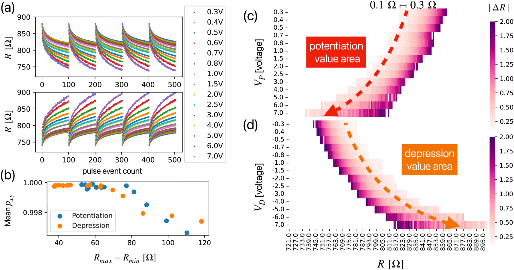 | ||
| Fig. 2 (a) Resistance switch achieved via identical pulses. During each potentiation and depression process, the device resistance is initially programmed to 880 Ω and 740 Ω, respectively. Then, the variety amplitude Vw and 2 s width write pulse is applied 100 times. (b) Metrics for the cycle-to-cycle reproducibility: in both the potentiation and depression processes, the mean value of the Pearson correlation coefficient between the last resistance R and every preceding resistance R is used for calculation. Resistance change (|ΔR|) after every programming pulse during (c) potentiation and (d) depression processes. | ||
Here, x and y represent two arrays of length n, with pxy assessing their correlation. ![[x with combining macron]](https://www.rsc.org/images/entities/i_char_0078_0304.gif) and ȳ represent their mean value. A pxy value of 1 indicates a perfect correlation between the datasets. Fig. 2(b) illustrates the relationship between the RS dynamic range (Rmax–Rmin) and pxy, calculated after every 100 write pulse operations. The mean pxy is computed by averaging the pxy values between the final RS array and all preceding RS arrays under identical Vw conditions. The pxy values approaching “1” demonstrate our device's exceptional cycle-to-cycle endurance, ensuring the reliability and reproducibility of RS characteristics for specific resistance levels under consistent Vw inputs. However, we observed an inverse relationship between the dynamic range and cycle-to-cycle endurance, with larger dynamic ranges leading to diminished endurance. Considering this trade-off, we opted for a relatively narrow dynamic range to prioritize high cycle-to-cycle endurance, thereby enhancing the precision of the RS process.
and ȳ represent their mean value. A pxy value of 1 indicates a perfect correlation between the datasets. Fig. 2(b) illustrates the relationship between the RS dynamic range (Rmax–Rmin) and pxy, calculated after every 100 write pulse operations. The mean pxy is computed by averaging the pxy values between the final RS array and all preceding RS arrays under identical Vw conditions. The pxy values approaching “1” demonstrate our device's exceptional cycle-to-cycle endurance, ensuring the reliability and reproducibility of RS characteristics for specific resistance levels under consistent Vw inputs. However, we observed an inverse relationship between the dynamic range and cycle-to-cycle endurance, with larger dynamic ranges leading to diminished endurance. Considering this trade-off, we opted for a relatively narrow dynamic range to prioritize high cycle-to-cycle endurance, thereby enhancing the precision of the RS process.
When setting the write pulse voltage, |ΔR| represents the change in resistance caused by a single write pulse. Fig. 2(c) and (d) show the values of |ΔR| that can be achieved with different magnitudes of Vw for each resistance level between the HRS and LRS during the potentiation and depression processes, respectively. For a given resistance value, an appropriate Vw can be determined by selecting the desired range of |ΔR|. This study defines the suitable range as 0.1 Ω < |ΔR| < 0.3 Ω. The upper limit of 0.3 Ω is set because we aim to precisely adjust the resistance change of the device with each pulse event to establish more program levels. The lower limit of 0.1 Ω is chosen because, for minimal resistance changes, the influence of noise becomes dominant. This range ensures that the device's resistance can be finely tuned without being overwhelmed by noise, thus achieving linear and precise adjustments in resistance levels. Furthermore, to maintain the reproducibility of resistance changes concerning the applied write voltage, this method requires the device to exhibit good cycle-to-cycle endurance characteristics.
Feedforward pulse scheme for potentiation and depression
To achieve linear RS characteristics in memristors, we scheme to select appropriate write voltages corresponding to different resistance states, as the resistance update curves will typically reach saturation at constant write voltages. Using the aforementioned relationship between the resistance value and |ΔR| [Fig. 2(c) and (d)], we can employ a FFP to tune the memristor. Fig. 3(a) illustrates the systematic approach of this scheme: the current resistance value (rFF) is obtained using a read pulse, and a 0.8 s duration write pulse with the appropriate voltage, Vw(rFF) is applied. Although shorter write pulse durations can create more program levels, they increase the tuning time. The results of continuous potentiation and depression using the FFP are plotted in Fig. 3(b). The average power consumption per potentiation and depression process is 240.7 mW and 114.6 mW, respectively (see ESI†). Since our device size is 15 μm, scaling down the device to the nanometer order will significantly reduce the power consumption. During the first depression process, the Vw values for each pulse event are plotted in different colors in Fig. 3(c). Throughout the potentiation and depression processes, the pulse event count for potentiation is 494 ± 11, and for depression, it is 579 ± 17, forming comparatively symmetrical RS characteristics. Higher symmetry might be achievable by reconfiguring the values of the LRS and HRS. | ||
| Fig. 3 (a) Systematic using the feedforward pulse scheme. (b) RS characteristics performed by the feedforward pulse scheme. (c) Detailed voltage application for the first depression process in (b). (d) Multilevel resistance segmentation result for a level count, n = 32. Two “red star” marks indicate details of the actual voltage application pulse events. | ||
Based on the RS characteristics data obtained via the FFP, we can further calibrate the pulse events to achieve linear resistance updates. Fig. 3(d) shows that by applying a multilevel resistance segmentation method (see the Experimental section) to the pulse events in Fig. 3(c), multiple pulse events are consolidated into a single pulse event, resulting in segments of resistance update characteristics with a higher linearity, Ra with highly reliable 32 program levels (5 bits) [see Fig. S3, ESI†]. For example, in Fig. 3(d), the two program levels indicated by “red stars” are achieved from the previous program level by applying the pulses shown in the inset diagram, as directed by the arrows. Next, using the multilevel resistance segmentation method, the Ra with 512 (9 bits), 128 (7 bits), and 32 (5 bits) program levels from the potentiation and depression processes are plotted in Fig. 4(a) and (b). By fitting the RS pulse event curves with eqn (2) and (3), the calculated vp and vd can be used to evaluate the nonlinearity of the device's RS characteristics.38–40
 | (2) |
 | (3) |
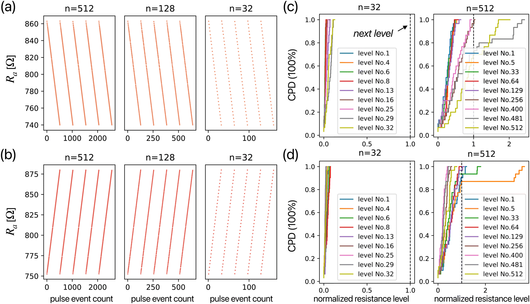 | ||
| Fig. 4 Multilevel resistance segmentation result of setting the level count as n = 512, n = 128, and n = 32 for (a) potentiation and (b) depression processes. Selected multi-level resistance settings for n = 32 and n = 512 configurations on (a) potentiation and (b) depression processes are randomly chosen and evaluated using the cumulative probability density (CPD) plots, which are displayed in (c) and (d), respectively. The vertical dashed line at the “normalized resistance level” = 1 represents the next level for the current program level. | ||
The reliability of individual multi-level settings is verified by cumulative probability density (CPD) plots shown in Fig. 4(c) and (d). The 66 samples from the RS process are used for the CPD analysis. To compare the program levels for n = 32 and n = 512, nine random potentiation and depression processes corresponding to resistance levels are normalized based on the current and the next resistance level, normalized between 0 and 1. For n = 512, in the high resistance region on potentiation (c) and low resistance region on depression (d), the horizontal axis of the CPD values are more likely to exceed 1, meaning that the level is easier to be “skipped.” This is likely due to extra ion diffusion caused by the Joule heating effect41,42 on the bulk-type device, as well as resistance overshoots due to different Vw values (see the ESI†). Additionally, based on the statistical analysis of all data, we define program levels with a “normalized resistance level” > 1 at a CPD = 80% as the program levels have a tendency to be skipped. In n = 32, the number of such levels is 0. In contrast, in n = 512, there are 117 levels for the potentiation process and 8 for the depression process. Despite this, the Non-Linearity Factor (NLF) remains at a very low level of 0.0009 for the depression process and 0.001 for the potentiation process. The higher error in potentiation compared to depression can also be observed in the global program level evaluation [Fig. S4, ESI†]. As the value of n increases, the program levels displayed by the CPD show greater variation, which impacts the reliability when used as a multi-bit memory. However, an increase in n also means more program levels, which represent a higher numerical precision in the computation. Therefore, in numerical computations, the errors introduced by setting the program levels and the quantization errors due to numerical precision are in a trade-off relationship. Choosing the appropriate program level based on the device's RS characteristics is essential in the design of memristor-based ANNs.
Image recognition ANN using the device characteristic
The accuracy of devices tuned by the FFP method is then validated in ANN computation applications. The program error, which occurs when setting the target resistance, can be simulated using the value sampler (see the Experimental section). Fig. 5(a) shows the generated results for the potentiation process (worst-case), where the actual resistance values yactual are generated based on the normalized target resistance values yideal with included program errors. Ideally, yideal and yactual would correspond to the straight red dashed line. But in reality, the resistance value setting errors |ri − ra| lead to the greater dispersion of yactual. The error, which comes from the device, is dominated in the magnified HRS region [Fig. 5(b)], and the quantization error due to bit precision is dominated in other magnified regions [Fig. 5(c)]. Thus, program errors can be estimated by a random sampling of errors caused by RS non-linearity and an error due to numerical quantization. We used program errors to simulate two different applications of setting up ANNs with a memristor crossbar array, as shown in Fig. 5(d) and (e). Weight transfer involves mapping trained model parameters onto the resistance of the crossbar array, while in-memory training performs forward and backward propagation calculations directly within the crossbar array, updating each device's weight in real time. | ||
| Fig. 5 (a) Program error generation results for the potentiation process, considered the worst case while segmenting the resistance levels to 5 bits (n = 32), 7 bits (n = 128), and 9 bits (n = 512). The zoomed detail highlights the value areas at (b) the HRS and (c) other regions. To evaluate the ANN benchmark according to device performance, the systematic approaches of (d) the weight transfer method and (e) the in-memory training method are illustrated. | ||
We constructed three image recognition ANNs of varying complexity for image classification tasks using diverse datasets: MNIST,43 Fashion-MNIST,44 and Caltech101.45 The architectures of these ANNs are illustrated in Fig. 6(a)–(c), with their parameters summarized in Table 1. The first neural network is a multilayer perceptron (MLP)46 with two hidden layers comprising 256 and 128 neurons, respectively. The second network is LeNet-5,5 with two convolutional layers having depths of 16 and 32, and the third network is ResNet-34,4 with 34 convolutional layers. Fig. 6(d) illustrates the accuracy of ANNs via the weight transfer method using different program levels. The horizontal dashed lines (pink, green, and azure) represent the accuracy achieved by training on digital devices (GPU). Although larger models can perform better on complex datasets, the computational accuracy of analog devices leads to amplified propagation errors in deeper networks and more frequent program errors with increasing weight parameters. As a result, to approximate GPU training results, an MLP architecture mapped to an analog device requires only 3 bits to achieve 95.2% accuracy, LeNet-5 requires 4 bits to achieve 86.9% accuracy, and ResNet-34 requires 8 bits to achieve 95.5% accuracy. Although increasing the number of program levels introduces higher errors in individual program level values [Fig. S2, ESI†], we find that maximizing the number of program levels is more effective for improving ANN accuracy. This outcome may be attributed to the excellent cycle-to-cycle endurance of our device, which indirectly ensures that quantization errors across most resistance ranges remain at a low level, as shown in Fig. 5(c).
 | ||
| Fig. 6 Image recognition results were obtained using the characteristics of a four-terminal TiO2−x device. The neural network diagrams illustrate the ANN type as (a) MLP, (b) LeNet-5 and (c) ResNet-34. The detailed parameters of the ANN architectures are shown in Table 1. (d) The device benchmark using the weight transfer method with different bit precisions applied. The device benchmark using the in-memory training method for the MNIST dataset and the Fashion MNIST are illustrated in (e) and (f), respectively. | ||
| Dataset | Architecture | Input shape | Output class | Layers | Parameters |
|---|---|---|---|---|---|
| MNIST | MLP | 28 × 28 | 10 | 2 | 202![[thin space (1/6-em)]](https://www.rsc.org/images/entities/char_2009.gif) 364 364 |
| Fashion-MNIST | LeNet-5(CNN) | 28 × 28 | 10 | 4 | 80064 |
| Caltech101 | ResNet-34(CNN) | 3 × 256 × 256 | 101 | 35 | 21336485 |
Fig. 6(e) and (f) illustrate the accuracy of in-memory training for ANNs using MLP and LeNet-5 architectures. The in-memory training results for ResNet-34 are omitted because, under our program error settings, the accuracy could not be improved during the gradient update. The blue line represents the training curve considering only the ADC/DAC effects and circuit noise, excluding program errors. The blue and orange dashed lines represent training curves using 4-bit and 9-bit program levels, respectively. Due to the lower computational precision of analog-based devices compared to the 64-bit double precision used by GPUs, in-memory training with memristors demands higher analog precision than weight transfer. For the MLP architecture, both 4-bit and 9-bit program levels achieve nearly 85% accuracy, but in the more complex LeNet-5 architecture, only the 9-bit program level can approach the ideal performance. For the ResNet-34 with 20 M parameters, significantly more than 9-bit program levels are required to achieve effective in-memory training. This precision requirement can be attributed to the amplification of noise effects during differential computations, which will disrupt proper gradient updates. While both weight transfer and in-memory training methods can map ANN weights onto memristor devices, in-memory training offers broader applicability in AI applications. One of the advantages of in-memory training is that it extends the use of memristive devices to real-time AI applications on edge devices and facilitates hardware-aware training to optimize retention errors. Additionally, in-memory training leverages fully memristor-based computation, consuming less power than weight transfer approaches.
We have demonstrated the FFP method on a high cycle-to-cycle endurance device, achieving linear resistance updates with a 9-bit programming resolution. An overview of the current research on the HRS/LRS ratio and the number of resistance levels in the devices21–28 is presented, categorizing the devices into filament-switching memristors and bulk-switching memristors, as plotted in Fig. 7. To increase the number of resistance levels, the most straightforward approach is to expand the device's dynamic range, which means increasing the HRS/LRS ratio. Conversely, in this study, we achieve a high-level control of RS characteristics through the mechanism of controlling bulk-switching using a four-terminal memristor32,33,47 and implemented FFP device tuning method, enabling the realization of 512 resistance levels even at a very low HRS/LRS ratio at 1.19. In bulk-type memristors, unlike filament-type ones, the RS rely on ion distribution and can achieve a higher number of resistance levels. To highlight the characteristics of bulk-type memristors, we propose a novel design approach that enhances multi-level performance by focusing on controlling ion drift rather than increasing the HRS/LRS ratio. Additionally, both our study and ref. 21 demonstrate that utilizing optimized write pulses, rather than identical pulses, improves the linearity and resistance level potential of the device. The analog memristor controlled by FFP can achieve a higher number of resistance levels, enhancing efficiency in multi-bit memory and AI edge devices. The ability of FFP to separate more program levels under a fixed HRS/LRS ratio relies on the device having good cycle-to-cycle and device-to-device variations. Future efforts to apply the FFP scheme to crossbar devices should focus on fabricating crossbar integration devices while ensuring that these characteristics are maintained. From the perspective of a single device, bulk-type memristors deterministically control the distribution of ion dopants through the applied write voltage, reducing randomness in the RS process. Therefore, as same as our TiO2−x-based devices, bulk-type memristors generally show good cycle-to-cycle endurance and low device-to-device variance [see Fig. S2 in the ESI†]. However, as a common issue for bulk-switching devices, the high-temperature operation caused by Joule heating effects affects the retention characteristics of our device [see Fig. S5, ESI†]. Such Joule heating effects influence the movement of dopant ions in our device, adversely affecting cycle-to-cycle variations and retention characteristics. Reducing the device temperature helps improve the retention characteristics of bulk-type memristors.37 To address this, we can introduce modulation techniques,34,48–50 which employ additional signals to regulate the RS speed. Incorporating this mechanism could allow us to reduce write voltages to mitigate Joule heating effects while maintaining the On/Off ratio. Additionally, time drift errors due to retention can also be corrected using in-memory training [Fig. 5(e)], and other in situ training algorithms.51 Regardless of this, the FFP scheme can be applied to other memristors, particularly to bulk-type memristors, which are expected to further enhance the precision and increase the number of program levels.
 | ||
| Fig. 7 Characteristics of the HRS/LRS ratio and the number of resistance levels of multi-level analog memristors reported to date. | ||
Meanwhile, our ANN simulation results indicate that the precision of program levels and the number of program levels are critical metrics for crossbar devices to achieve deeper neural network computation. To handle the complexity of AI models, even devices with 9-bit program levels may face challenges, particularly in “in-memory training” scenarios. By applying the FFP scheme combined with the bulk-switching mechanism, we can improve the linearity characteristics affected by the program level, enabling the current device to meet the growing complexity of AI models, and paving the way for utilizing memristors in practical AI applications.
Conclusions
This study presents an FFP method, with the concept of proactively calibrating the RS characteristics for each resistance value and effectively regulating the RS change rate concerning the number of pulse events. As a demonstration, we apply the FFP scheme on a four-terminal bulk-type memristor device with high cycle-to-cycle endurance and achieve precise resistance switching control with 512 program levels at a low HRS/LRS ratio of 1.19, maintaining 10−3 RS nonlinearity metrics. This method is compatible with other memristor devices and can facilitate an increased number of program levels while ensuring the device's linearity. Moreover, we have devised an analog-based ANN accuracy assessment framework for the FFP-tuned device. This framework accounts for device linearity through specific metrics, including resistance setting errors caused by RS nonlinearity and quantization errors arising from program-level limitations. Using weight transfer, we estimate that the analog computing accuracy of our device achieves 95.5% accuracy in ResNet-34 with 21336485 parameters across 34 layers. Our accuracy evaluation in in-memory training indicates that for deeper neural networks capable of processing complex datasets beyond MNIST, a program level on the order of 500 remains insufficient to achieve the same level of accuracy as digital-based processing units. Therefore, for future applications involving deeper ANNs, the number of program levels that affect computing accuracy will become increasingly important.
Experimental section
Memristive device fabrication
A (001) rutile-type insulating TiO2 single-crystal substrate was used for memristor device fabrication. A TiO2−x epitaxial thin film, serving as the resistive switching layer, was deposited on a substrate using pulsed laser deposition at 500 °C, under typical conditions of an oxygen partial pressure of 1.0 × 10⁻⁴ Pa to achieve a thickness of 40 nm. The electrodes were patterned using electron beam lithography followed by Pt deposition by electron beam evaporation and a lift-off process. An SiO2 insulating layer (100 nm) was deposited using RF sputtering and then patterned and etched to create contact holes.Device measurements
Measurements were conducted using a Keithley 3706A system switch/multimeter and a Keysight B1500A semiconductor device analyzer at room temperature under air conditions. The measurement system was home-built in Python, with the instrument control facilitated via the Virtual Instrument Software Architecture (VISA) protocol. Standard Commands for Programmable Instruments (SCPI) were employed for the Keysight B1500A, and Test Script Processor (TSP) commands were utilized for the Keithley 3706A to automate and program the measurement processes. The resistance write process involved applying a pulse voltage to terminals T2 and T4, with T1 and T4 grounded. For the resistance read process, a pulse voltage of 0.1 V was applied to T1, while T2, T3, and T4 were grounded. Although currents from T1 to T2, T3, and T4 can be measured separately, the device resistance was calculated based on the current measured between T1 and T3. To clearly distinguish a large number of resistance levels on our device, the order of 100 nA current measurement resolution is required. For such a high-precision measurement, the resolution of Keysight B1500A is set at 10 nA and the number of averaging samples for ADC is set at 11.Multilevel resistance segmentation method
To achieve a multilevel resistance, we utilized the FFP pulse application method shown in Fig. 3(a) to obtain the measured feedforward pulse events (RFF) [Fig. 3(c)]. To further enhance the linearity in RFF, all events of the feedforward pulse are segmented into several pulse event groups, each considered as one applied pulse. First, RFF is normalized to a range of 0 to 1. When the resistance level count is set to n, Ri = [ri,1, …, ri,n] as the target values for segmenting RFF and Ra = [ra,1, …, ra,n] as the actual segmented multilevel results. Here, ri,1 can be the low resistance state (rmin) and ri,n can be the high resistance state (rmax). For a target resistance level ri,j, the index value m in array RFF is calculated by m = argmin|RFF − ri,j|, then ra,j = RFF[m]. At this point, to compute the write pulse (Vw) required to update the state from ri,j to ri,j+1, suppose the index of RFF corresponding to the state ri,j is mj and the index corresponding to the state ri,j+1 is mj+1, then the write pulse events are [Vw(rFF,mj),…,Vw(rFF,mj+1)]. For example, the inset figure in Fig. 3(d) shows the planning results for two write pulse events. In this planning, if it is insufficient to separate enough resistance levels in RFF, the states of the elements in Ri will remain unoccupied.Crossbar device simulations
We implement a framework of crossbar device simulations to compute the performance of AI applications. All networks are implemented in PyTorch.52 The tensor computing for training networks is performed in GPU, while the tensor computing for program error simulations is performed in the CPU and accelerated by Numba.53 To ensure the validity of the ANN benchmark, the dataset used for training and testing is fixed in each computation, and the random seed is not used to control the generated values in other random numeric generations. IBM aihwkit,54 an in-memory computing device simulation toolkit, is used to benchmark hardware-specific non-idealities of the four-terminal TiO2−x crossbar array. Blocks in digital ANN models are converted into analog blocks and mapped into crossbar tiles. The ADC/DAC non-idealities, forward noise during the analog-matvec computation, and custom device program error including non-linearity and bit precision have been taken into account. Errors due to time drift behavior and device-to-device variance are not considered in this work.Device program error sampler
Increasing the bit count in the digital domain enhances computational precision; however, our device characterization results indicate that it also exacerbates the non-linear factor, thereby diminishing computational accuracy. A custom device program error is implemented to assess the performance of the ANN relative to bit count and nonlinearity, considering the interplay between bit quantization and non-linearity.Prior to applying the program error, the resistance array, which represents the weight elements in the ANN neurons, is normalized to yideal. The actual value yactual, incorporating the device program error, is then randomly sampled as described in eqn (4). As an illustration, the correspondence between yactual and yideal for the potentiation case is depicted in Fig. 5(a)–(c).
| yactual = Q(yideal) + T(loc(yideal),s(yideal),ν(yideal)) | (4) |
Here, Q denotes the method for calculating the bit quantization value of yideal, while T represents a random variate in Student's t-distribution with the mean value loc, scale s and degree of freedom ν. For Q, the specific bit count and value range are set to determine the quantization target values. Each resistance value is designated as the argument ri,j in the “multilevel resistance segmentation method” to compute ra,j as the bit precision error. Additionally, the random value T is generated according to the probability density function as shown in eqn (5).

| T(loc,s,ν) = f(t,ν) × s + loc | (5) |
ANN weight transfer
As shown in Fig. 5(c), the weight transfer method involves training a full-precision (FP64) AI model on a GPU and then transferring the weight parameters from the ANN to the memristor device as resistance values. During this process, configuring the resistance of a device to match the ANN parameter weight w may result in deviations due to programming pulse errors. For our TiO2−x device characteristics, using FFP to control resistance switching (RS) leads to errors dependent on the weight values, as illustrated in Fig. S2(b) and (c) (ESI†). The relationship of this error after normalization can be expressed by the ideal value yideal corresponding to the sampled actual value yactual, shown in Fig. 5(a). When transferring ANN weights, we map the high resistance state (HRS) and low resistance state (LRS) of the memristor to weight values in the range of [−4, 4], considering the value ranges of the common output of each hidden layer in the AI model. In this ANN simulation, we convert the ANN to an analog ANN mapped in a memristor crossbar device and then calculate the analog ANN accuracy when the n state amounts are separated uniformly within this weight value range.In-memory training
As shown in Fig. 5(d), the in-memory training method involves using backpropagation55 to update the weights directly in the memristor array. First, the ANN is converted into an analog ANN that can be mapped to a memristor crossbar. In the forward pass of the analog ANN, the computation is performed by the voltage output of the memristor array instead of using a GPU. The loss of the memristor is then externally evaluated on the test dataset, and this loss is used to update the model gradient by reconfiguring the resistance of each memristor during the backward pass. The algorithm for updating analog ANN weights employs the AnalogSGD optimizer,56 which is implemented in IBM's aihwkit. For all training, the batch size is 64, the training epoch is 50, and the learning rate is 0.1, 0.01, and 0.0001 for each of the three models shown in Table 1.The in-memory training will introduce errors each time the weights are updated due to the memristor programming error and both the forward pass and backward pass will be affected. To represent this error, in addition to converting the ANN to an analog ANN model, we add a noise layer using the device programming error sampling method behind each block containing trainable weights [Fig. 5(d)]. Each noise layer generates values with the same shape as the input matrix, incorporating the device programming error values.
Author contributions
Zhuo Diao, Tetsuya Tohei, and Akira Sakai designed the study and conceived the analysis. Zhuo Diao implemented the algorithm, performed the simulations of the neural network framework, and wrote the main manuscript text. Ryohei Yamamoto and Meng Zijie fabricated and morphologically characterized the devices. Akira Sakai provided the funding support and conceptualization of the work. All authors reviewed the manuscript.Data availability
All relevant data are available from the authors on reasonable request and/or are included within the article and the ESI.†Conflicts of interest
There are no conflicts to declare.Acknowledgements
This research was supported in part by a KAKENHI Grant-in-Aid (no. JP23H01687, JP23K26380, JP24K21620 and JP24K00926) from the Japan Society for the Promotion of Science (JSPS).Notes and references
- F. Sebastiani, ACM Comput. Surv., 2002, 34, 1–47 CrossRef.
- A. Krizhevsky, I. Sutskever and G. E. Hinton, Proceedings of the 25th International Conference on Neural Information Processing Systems, Red Hook, NY, USA, 2012, vol. 1, pp. 1097–1105.
- S. Liu and W. Deng, 3rd IAPR Asian Conference on Pattern Recognition (ACPR), 2015, pp. 730–734.
- K. He, X. Zhang, S. Ren and J. Sun, IEEE Conference on Computer Vision and Pattern Recognition (CVPR), 2016, pp. 770–778.
- Y. Lecun, L. Bottou, Y. Bengio and P. Haffner, Proc. IEEE, 1998, 86, 2278–2324 CrossRef.
- J. Redmon, S. Divvala, R. Girshick and A. Farhadi, IEEE Conference on Computer Vision and Pattern Recognition (CVPR), 2016, pp. 779–788.
- H. Touvron, T. Lavril, G. Izacard, X. Martinet, M.-A. Lachaux, T. Lacroix, B. Roziere, N. Goyal, E. Hambro, F. Azhar, A. Rodriguez, A. Joulin, E. Grave and G. Lample, LLaMA: Open and Efficient Foundation Language Models, arxiv, 2023, preprint, https://arxiv.org/abs/2302.13971.
- R. Rombach, A. Blattmann, D. Lorenz, P. Esser and B. Ommer, Proceedings of the IEEE/CVF Conference on Computer Vision and Pattern Recognition (CVPR), 2022, pp. 10684–10695.
- N. C. Thompson, K. Greenewald, K. Lee and G. F. Manso, IEEE Spectrum, 2021, 58, 50–55 Search PubMed.
- E. Strubell, A. Ganesh and A. McCallum, Proceedings of the AAAI Conference on Artificial Intelligence, 2020, 34, pp. 13693–13696.
- S. Luccioni, Y. Jernite and E. Strubell, Proceedings of the 2024 ACM Conference on Fairness, Accountability, and Transparency, New York, NY, USA, 2024, pp. 85–99.
- D. B. Strukov, G. S. Snider, D. R. Stewart and R. S. Williams, Nature, 2008, 453, 80–83 CrossRef CAS PubMed.
- E. Masanet, A. Shehabi, N. Lei, S. Smith and J. Koomey, Science, 2020, 367, 984–986 CrossRef CAS.
- S. Ambrogio, P. Narayanan, H. Tsai, R. M. Shelby, I. Boybat, C. di Nolfo, S. Sidler, M. Giordano, M. Bodini, N. C. P. Farinha, B. Killeen, C. Cheng, Y. Jaoudi and G. W. Burr, Nature, 2018, 558, 60–67 CrossRef CAS PubMed.
- N. K. Upadhyay, H. Jiang, Z. Wang, S. Asapu, Q. Xia and J. Joshua Yang, Adv. Mater. Technol., 2019, 4, 1800589 CrossRef.
- V. K. Sangwan and M. C. Hersam, Nat. Nanotechnol., 2020, 15, 517–528 CrossRef CAS.
- C. Li, M. Hu, Y. Li, H. Jiang, N. Ge, E. Montgomery, J. Zhang, W. Song, N. Dávila, C. E. Graves, Z. Li, J. P. Strachan, P. Lin, Z. Wang, M. Barnell, Q. Wu, R. S. Williams, J. J. Yang and Q. Xia, Nat. Electron., 2018, 1, 52–59 CrossRef.
- P. M. Sheridan, F. Cai, C. Du, W. Ma, Z. Zhang and W. D. Lu, Nat. Nanotechnol., 2017, 12, 784–789 CrossRef CAS PubMed.
- Z. Shen, C. Zhao, L. Kang, Y. Sun, Y. Liu, I. Z. Mitrovic, L. Yang, E. G. Lim, Z. Zeng and C. Zhao, Adv. Intell. Syst., 2022, 4, 2100236 CrossRef.
- P. Yao, H. Wu, B. Gao, J. Tang, Q. Zhang, W. Zhang, J. J. Yang and H. Qian, Nature, 2020, 577, 641–646 CrossRef CAS PubMed.
- M. Rao, H. Tang, J. Wu, W. Song, M. Zhang, W. Yin, Y. Zhuo, F. Kiani, B. Chen, X. Jiang, H. Liu, H.-Y. Chen, R. Midya, F. Ye, H. Jiang, Z. Wang, M. Wu, M. Hu, H. Wang, Q. Xia, N. Ge, J. Li and J. J. Yang, Nature, 2023, 615, 823–829 CrossRef CAS PubMed.
- W. He, H. Sun, Y. Zhou, K. Lu, K. Xue and X. Miao, Sci. Rep., 2017, 7, 10070 CrossRef.
- T.-H. Kim, J. Lee, S. Kim, J. Park, B.-G. Park and H. Kim, Nanotechnology, 2021, 32, 295201 CrossRef CAS.
- S. Lee, J. Jeon, K. Eom, C. Jeong, Y. Yang, J.-Y. Park, C.-B. Eom and H. Lee, Sci. Rep., 2022, 12, 9068 CrossRef CAS.
- W. Banerjee and H. Hwang, Adv. Electron. Mater., 2019, 5, 1900744 CrossRef CAS.
- Y. Wu, Q. Wang, Z. Wang, X. Wang, B. Ayyagari, S. Krishnan, M. Chudzik and W. D. Lu, Adv. Mater., 2023, 35, 2305465 CAS.
- J. Park, A. Kumar, Y. Zhou, S. Oh, J.-H. Kim, Y. Shi, S. Jain, G. Hota, E. Qiu, A. L. Nagle, I. K. Schuller, C. D. Schuman, G. Cauwenberghs and D. Kuzum, Nat. Commun., 2024, 15, 3492 CAS.
- H. Cheng, E. R. Hsieh, Z. H. Huang, C. H. Chuang, C. H. Chen, F. L. Li, Y. M. Lo, C. H. Liu and S. S. Chung, International Symposium on VLSI Technology, Systems and Application (VLSI-TSA), 2018, pp. 1–2.
- Y. Li, S. Chen, Z. Yu, S. Li, Y. Xiong, M.-E. Pam, Y.-W. Zhang and K.-W. Ang, Adv. Mater., 2022, 34, 2201488 CrossRef CAS PubMed.
- A. Saleem, D. Kumar, F. Wu, L. B. Keong and T.-Y. Tseng, IEEE Trans. Electron Devices, 2023, 70, 1351–1358 CAS.
- N. Panwar, B. Rajendran and U. Ganguly, IEEE Electron Device Lett., 2017, 38, 740–743 CAS.
- R. Miyake, Z. Nagata, K. Adachi, Y. Hayashi, T. Tohei and A. Sakai, ACS Appl. Electron. Mater., 2022, 4, 2326–2336 CAS.
- S. Takeuchi, T. Shimizu, T. Isaka, T. Tohei, N. Ikarashi and A. Sakai, Sci. Rep., 2019, 9, 2601 Search PubMed.
- Z. Nagata, T. Shimizu, T. Isaka, T. Tohei, N. Ikarashi and A. Sakai, Sci. Rep., 2019, 9, 10013 CrossRef PubMed.
- M. Prezioso, F. Merrikh-Bayat, B. D. Hoskins, G. C. Adam, K. K. Likharev and D. B. Strukov, Nature, 2015, 521, 61–64 CrossRef CAS.
- K. Seo, I. Kim, S. Jung, M. Jo, S. Park, J. Park, J. Shin, K. P. Biju, J. Kong, K. Lee, B. Lee and H. Hwang, Nanotechnology, 2011, 22, 254023 CrossRef.
- T. Ikeuchi, Y. Hayashi, T. Tohei and A. Sakai, Appl. Phys. Express, 2023, 16, 015509 CrossRef.
- Y. Li, E. J. Fuller, J. D. Sugar, S. Yoo, D. S. Ashby, C. H. Bennett, R. D. Horton, M. S. Bartsch, M. J. Marinella, W. D. Lu and A. A. Talin, Adv. Mater., 2020, 32, 2003984 CrossRef CAS.
- J. Tang, C. He, J. Tang, K. Yue, Q. Zhang, Y. Liu, Q. Wang, S. Wang, N. Li, C. Shen, Y. Zhao, J. Liu, J. Yuan, Z. Wei, J. Li, K. Watanabe, T. Taniguchi, D. Shang, S. Wang, W. Yang, R. Yang, D. Shi and G. Zhang, Adv. Funct. Mater., 2021, 31, 2011083 CrossRef CAS.
- D. Xiang, T. Liu, X. Zhang, P. Zhou and W. Chen, Nano Lett., 2021, 21, 3557–3565 CrossRef CAS PubMed.
- M. Kim, D. Eun Kim, Y. Wang, D. Lee, D.-H. Lim, H. Choi, I. Kymissis, J. J. Yang, J. Suh, H.-S. Lee and H.-H. Park, Appl. Mater. Today, 2024, 38, 102204 CrossRef.
- B. J. Choi, D. S. Jeong, S. K. Kim, C. Rohde, S. Choi, J. H. Oh, H. J. Kim, C. S. Hwang, K. Szot, R. Waser, B. Reichenberg and S. Tiedke, J. Appl. Phys., 2005, 98, 033715 Search PubMed.
- K. Szot, W. Speier, R. Carius, U. Zastrow and W. Beyer, Phys. Rev. Lett., 2002, 88, 075508 CAS.
- L. Deng, IEEE Signal Process. Mag., 2012, 29, 141–142 Search PubMed.
- H. Xiao, K. Rasul and R. Vollgraf, Fashion-MNIST: a Novel Image Dataset for Benchmarking Machine Learning Algorithms, 2017 Search PubMed.
- F.-F. Li, M. Andreeto, M. Ranzato and P. Perona, Caltech101, 2022.
- D. E. Rumelhart, G. E. Hinton and R. J. Williams, Nature, 1986, 323, 533–536 CrossRef.
- T. Ahmed, M. Tahir, M. X. Low, Y. Ren, S. A. Tawfik, E. L. H. Mayes, S. Kuriakose, S. Nawaz, M. J. S. Spencer, H. Chen, M. Bhaskaran, S. Sriram and S. Walia, Adv. Mater., 2021, 33, 2004207 CAS.
- L. Hu, J. Yang, J. Wang, P. Cheng, L. O. Chua and F. Zhuge, Adv. Funct. Mater., 2021, 31, 2005582 CAS.
- X. Shan, Z. Wang, J. Xie, J. Han, Y. Tao, Y. Lin, X. Zhao, D. Ielmini, Y. Liu and H. Xu, Adv. Sci., 2024, 11, 2405160 CrossRef CAS PubMed.
- T. Gokmen and W. Haensch, Front. Neurosci., 2020, 14, 00103 Search PubMed.
- A. Paszke, S. Gross, F. Massa, A. Lerer, J. Bradbury, G. Chanan, T. Killeen, Z. Lin, N. Gimelshein, L. Antiga, A. Desmaison, A. Kopf, E. Yang, Z. DeVito, M. Raison, A. Tejani, S. Chilamkurthy, B. Steiner, L. Fang, J. Bai and S. Chintala, PyTorch: An Imperative Style, High-Performance Deep Learning Library, 2019, https://arxiv.org/abs/1912.01703.
- S. K. Lam, A. Pitrou and S. Seibert, Proceedings of the Second Workshop on the LLVM Compiler Infrastructure in HPC, New York, NY, USA, 2015.
- M. J. Rasch, D. Moreda, T. Gokmen, M. Le Gallo, F. Carta, C. Goldberg, K. El Maghraoui, A. Sebastian and V. Narayanan, IEEE 3rd International Conference on Artificial Intelligence Circuits and Systems (AICAS), 2021, pp. 1–4.
- D. E. Rumelhart, G. E. Hinton and R. J. Williams, Nature, 1986, 323, 533–536 CrossRef.
- T. Gokmen and Y. Vlasov, Front. Neurosci., 2016, 10, 00333 Search PubMed.
Footnote |
| † Electronic supplementary information (ESI) available. See DOI: https://doi.org/10.1039/d4nh00623b |
| This journal is © The Royal Society of Chemistry 2025 |