
Enhanced piezoresponse in van der Waals 2D CuCrInP2S6 through nanoscale phase segregation†
Sharidya
Rahman
 *ab,
Sanika S.
Padelkar
abcde,
Lan
Nguyen
ab,
Naufan
Nurrosyid
ab,
Md Hemayet
Uddin
f,
Oleksandr
Chernyavskiy
g,
Junlin
Yan
ab,
Chang
Cao
ab,
Alexandr N.
Simonov
d,
Aftab
Alam
ce and
Jacek J.
Jasieniak
*ab
*ab,
Sanika S.
Padelkar
abcde,
Lan
Nguyen
ab,
Naufan
Nurrosyid
ab,
Md Hemayet
Uddin
f,
Oleksandr
Chernyavskiy
g,
Junlin
Yan
ab,
Chang
Cao
ab,
Alexandr N.
Simonov
d,
Aftab
Alam
ce and
Jacek J.
Jasieniak
*ab
aDepartment of Materials Science and Engineering, Monash University, Clayton, VIC 3800, Australia. E-mail: sharidya.rahman@monash.edu; sharidya.rahman@alumni.anu.edu.au; jacek.jasieniak@monash.edu
bARC Centre of Excellence in Exciton Science, Monash University, Melbourne 3800, Australia
cDepartment of Physics, Indian Institute of Technology, Bombay, Powai, Mumbai 400076, India
dSchool of Chemistry, Monash University, Victoria 3800, Australia
eIITB-Monash Research Academy, IIT Bombay, Mumbai 400076, India
fMelbourne Centre for Nanofabrication, Australian National Fabrication Facility (Victorian Node), 151 Wellington Road Clayton, VIC 3168, Australia
gMonash Micro Imaging, Monash University, Clayton, VIC 3800, Australia
First published on 25th March 2025
Abstract
van der Waals metal chalcogen thiophosphates have drawn elevated interest for diverse applications, including energy harvesting, electronics and optoelectronics. Despite this progress, the role of nanoscale ion migration in complex intermediary thiophosphate compounds has not been well understood, resulting in their structure–property characteristics remaining elusive. Herein, we focus on copper-deficient CuCrInP2S6 as a prototypic layered thiophosphate compound to address this shortcoming. Piezo force microscopy reveals that this material exhibits unusual cage-like domain networks with an enhanced piezo response at the domain boundaries. The associated piezoelectric coefficient d33 is found to be among the highest across reported van der Waals multi-layered materials. These results are further complemented with Kelvin probe microscopy and second harmonic generation spectroscopy that disclose significantly elevated non-linear optical emission along these domain boundaries. Ab initio calculations performed in conjunction with nudge elastic theory provide a deeper insight into the diffusion processes responsible for these observed phenomena. These findings shed new light into intermediary thiophosphate based 2D compounds, highlighting future prospects towards their use in emergent piezoelectric based technological applications.
New conceptsVan der Waals metal chalcogen thiophosphates are an emerging class of 2D materials that have tremendous promise for a variety of optoelectronic and energy harvesting applications. This project delves into the intriguing properties of one such novel but unexplored material, CuCrInP2S6 (CCIPS), showing that when isolated as nanosheets, intricate nanoscale copper segregation creates cage-like domains that exhibit unique piezoelectric properties at room temperature. A key finding of the work is that the out-of-plane piezoelectric coefficient is 12-fold higher at the copper-rich domain boundaries. These domain-boundary piezoelectric properties of CCIPS are superior compared to many other traditional bulk or multilayer van der Waals materials, as well as nitride and arsenide-based semiconductors and Janus materials studied to date. To further understand the origins of the domain formation, density functional theory (DFT) simulations and ab initio studies have provided theoretical insights into the Cu ionic migration within the crystal structure. The findings highlight the comparatively high hopping probability of copper compared to all other elements in CCIPS, while also showing that the Bader charge on chromium can change to accommodate this diffusion process by enabling local charge neutrality. Our findings highlight the potential of CCIPS for advanced piezoelectric applications like sensors and energy harvesters. |
Introduction
Since the discovery of graphene in 2004,1 the field of two-dimensional (2D) layered materials has broadly expanded to incorporate the majority of the elements in the periodic table.2,3 Driven by their elusive unconventional physics, such materials have been explored in multifarious applications,4,5 including photodetectors,6,7 solar cells,8,9 single photon emitters,10 memory devices and spintronic devices.11–13 Across these, 2D materials have harnessed quantum size effects due to their nano thicknesses to exhibit a diverse range of unique optical, electrical, mechanical and chemical properties,14–16 that are otherwise absent in their bulk counterparts. Furthermore, 2D materials possessing a non-centrosymmetric structure with piezoelectric properties can enlighten distinct applications in nanomechanical and electronic devices,17 which have broad applicability from medical and healthcare sectors to aerospace and defense.18–20Piezoelectricity refers to the ability of materials to generate electric polarization charges under the application of external mechanical stress or electrical bias. A plethora of materials have been reported to possess piezoelectricity, including crystals, ceramics, polymers, semiconductors, composites and bi-molecules, with many finding potential applications in actuators, sensors and energy harvesters.21–23 However, demand for small scale and miniaturized piezoelectric devices with multi-functional properties have led to rapid progress in the field of 2D nanomaterial based piezoelectrics. This is mostly due to their ultrathin architecture, dangling-bond free interfaces, impressive electromechanical response, bandgap tunability, inherently strong and flexible structure and presence of free charges that can be manipulated electrostatically.15,24 Further, 2D materials are fully compatible with current microfabrication technologies that underpin current thin-film manufacturing techniques for the semiconductor industry. This allows devices featuring 2D material to be co-integrated with conventional integrated circuits or electromechanical systems.25
While graphene, transition metal dichalcogenides (TMDs), hexagonal boron nitride (hBN) and black phosphorus have been the building blocks for the advancement of 2D material, several new compounds have emerged with long range ferroic orders and other intriguing properties.26 Among them, the transition metal thiophosphates (TMPs) have attracted proliferated interests owing to their piezoelectricity and ionic conductivity.27,28 In addition they provide a stable platform for incorporating multiple transition atoms into a single structure and exploiting only the required physical properties for specific applications. TMPs belong to a broad class of van der Waals (vdW) layered solids with a general chemical formula of M1M2P2X6, where M1 and M2 are usually the different transition metal ions (i.e., Cu, Cr, Ag, In, Bi, etc.) and X is a chalcogen. They are dielectric in nature, exhibiting intriguing non-linear optical, electric and magnetic properties. For instance, CuInP2S6 (CIPS) has attracted immense attention, partly due to its robust RT piezoelectricity, where spontaneous ordering of electric dipoles produces macroscopic polarization, switchable through an external electric field.29 These materials have also demonstrated polarization states that are sensitive to temperature, pressure and bias, as well as possessing high negative longitudinal piezoelectric coefficients (d333) of more than −15 pm V−1.27 Such properties are attractive for pyroelectric applications,30 as well as non-volatile memory and solid state devices.31
CuCrP2S6 (CCPS) exhibits a similar crystal structure to CIPS and belongs to the same class of compounds. More often it is multiferroic in nature, producing distinct phases at different temperatures.32,33 This is mainly due to the substitution of diamagnetic In3+ ions with the paramagnetic Cr3+ ions leading to both magnetism and piezoelectricity. Detailed reports have emerged outlining the phase transition temperatures of CCPS and its intrinsic RT ferroelectricity in the 2D limit.34 This broadens the applications of TMPs to low dimensional multiferroic devices.
A more complex case arises in intermediary but stable phases between CIPS and CCPS, involving the presence of three transition metal ions, namely vdW layered CuCrInP2S6 (CCIPS). This can lead to the existence of multiple phases at room temperature owing to the presence of both In and Cr ions, paving way for multifunctional miniaturized electronic devices.21 CCIPS can be expected to exhibit unique polar physics, similar to its parent compound, such as out-of-plane polarization, quadruple potential wells and even piezoelectric domain boundaries.27,35 Investigations of such intermediary compounds have been limited to dipolar glass and solid solution phases where researchers have focused on ferroic fluctuations and perturbations.36 Dopant distribution have also been examined using aberration corrected electron microscopy with an aim to understand the spin-dipole ordering.37 However, to date there has been no direct evidence of domain wall formation and phase segregation in vdW CuCrInP2S6. As such, a comprehensive understanding of its non-centro symmetric structure along with its piezoelectric properties remains underexplored. While ionic migration has been examined in CIPS through conductive mapping, the accompanying nanoscale electronic and optical properties for intermediary CCIPS is still lacking. Prior experimental work on 2D MTPs motivated us to explore whether robust RT phase-selective piezoelectricity may exist in layered CCIPS. Scrutinizing the nature of piezoelectric response and underlying principles in intrinsic vdW layered CCIPS is of fundamental significance for realizing novel physical properties that can be harnessed in practical devices operating at room temperature.
Here we study delaminated bulk CuCrInP2S6 using quantitative nanoscale imaging of its piezoelectric properties and identify the unusual formation of nanoscale cage-like domains. It is found that the domain boundaries manifest an elevated out-of-plane piezoelectric amplitude with up to three-fold enhancement compared to the domain regions. Consequently, the vertical piezoelectric coefficient (d33) was measured and found to increment by at least twelve-fold along the domain boundaries. This indicates a higher vertical displacement in these regions which is essential for applications in piezotronics, nano-electromechanical systems and energy converters.21,38 Such elusive domain formation has been further correlated with Kelvin probe force microscopy (KPFM) measurements, revealing similar variation in surface work function. In addition, the domain network also manifests an increase in second harmonic generation (SHG). Such behavior can be explained using copper (Cu) displacement and hopping mechanisms, allowing the mobile ion to occupy different crystallographic sites resulting in phase segregation. This is further substantiated using first principles calculations based on nudge band elastic theory. This work provides a deeper insight into the nanoscale ionic migration in vdW intermediary CCIPS, paving the way for next generation electronics paradigm.
Results and discussion
Crystal structure of CCIPS
Multiple optical spectroscopies were performed to examine the crystal structure and confirm the pristine quality of CCIPS flakes. Fig. 1a displays the top and side view of the CCIPS crystal structure. The vdW layered compounds feature an ABC close packed structure consisting of a hexagonal sulphur framework, where the centre of the octahedral voids is mutually occupied by Cu, Cr and In cations, in addition to P–P pairs that are inherent to the P2S62− complexes. This forms a periodic triangular pattern within a single layer. Bulk crystals are mainly composed of vertically stacked layers, held by weakly interacting vdW forces. A complete unit cell depicting the material symmetry, generally includes two adjacent layers, owing to the exchange in site between the cations and P–P pairing. X-ray diffraction (XRD) analysis (Fig. 1b) confirms the high crystallinity of the commercially sourced and exfoliated CCIPS crystals (see Methods section). Four sharp peaks are displayed at 14.35°, 28.35°, 41.69° and 56.6°, corresponding to (002), (004), (006) and (008) planes, respectively. These are consistent with the hexagonal structure of its parent compounds, CCPS and CIPS.34,39Fig. 1c shows the SEM based energy dispersive X-ray spectrometry (EDS) spectrum, confirming the presence of the elemental composition, while also verifying the deficiency of Cu (see also ESI† Table S1). Repeatable results were obtained across multiple samples showing distinct energy lines for Cu, Cr, In, P and S. | ||
| Fig. 1 Characterization of CuCrInP2S6 (CCIPS) single crystals: (a) molecular schematic showing the top and side view of the crystal structure of vdW 2D CCIPS. Each atom is represented with different colors for distinction. (b) A photo of a bulk CCIPS crystal followed by a typical optical image of a 2D CCIPS sample exfoliated mechanically from the bulk crystal and transferred to a Si substrate using vdW transfer method. (c) The measured XRD pattern for an as-obtained CCIPS single crystal with ab crystalline planes. All XRD peaks are indicative of strong crystallinity and existence of intermediary phase consisting of both Cr and In. (d) EDS spectrum taken from a bulk sample, with clear evidence for the presence of Cu, Cr, In, P and S. Si is observed as background signal from the substrate. (e) Raman spectrum taken from a bulk sample using 532 nm green laser at RT. Multiple vibrational signatures indicates the presence of a complex intermediary phases. Raman signal taken from the bare Si/SiO2 substrate is used as reference. (f) Nanoscale TEM-EDS elemental mapping of a small area CuCrInP2S6 bulk sample. Cu mapping manifests the domain formation, signifying ionic Cu migration and phase segregation. Scale bar is 200 nm for all maps. | ||
Fig. 1e shows the Raman spectrum of the exfoliated sample, showing a complex combination of phonon peaks. Typically, the extended vibrational modes between 100 and 350 cm−1 partly involve vibrations of the metal cations and deformation of the octahedral cages incorporating the displacement of anions. Out-of-plane vibrations of P–P dimers and S valence vibration, dominates the strong sharp peak at around ∼376 cm−1. The high frequency modes between 450–600 cm−1 are mostly dominated by P–P valence vibrations in the out-of plane direction, which may also have a dwindled contribution from in-plane stretching of sulphur atoms (PS3 stretching modes).40,41 Peaks at 102, 108 and 312 cm−1 can be associated with vibration of Cu ions, while the modes at 125.6, 138.6 and ∼298 cm−1 to that of In ions. The low energy modes at ∼102.2 and 125 cm−1 are also motivated by the out-of-plane rocking motion of the S atoms within the octahedra and out-of-plane vibrations of the P–P dimers, respectively; this is further escorted by commensurate displacements of the Cu and In ions in the out-of-plane direction.36 Signatures at ∼204, ∼254.3, 269.1 and 282.8 cm−1 materialize mostly from the deformation of the S–P–P and S–P–S bonds [δ(SPP) and δ(SPS)] and are mostly known as anion deformation modes. The two former signatures correspond to PS3 group rotation and translation, typically present in CuCrP2S6 compound.33,36 Furthermore, peaks at 254.3 and 282 cm−1 could also be dispensed by in-plane and out-of-plane vibrations of Cr and S bonds.42,43 The presence of different metal cations and their locations in the octahedra sometimes influence the anion deformation modes resulting in a slight variation in their spectral wavenumbers.41 The peak at ∼312.7 cm−1 can be attributed to distortions within the hexagonal sulphur cage occupied by the Cu+ cations. Some Raman active modes of the cations falls below the 100 cm−1 and was outside our detection range.44 Collectively, this analysis confirms the key elemental signatures of CCIPS within the exfoliated films and the associated hexagonal close-packed structure.
To further investigate the surface structure and chemical composition of bulk CCIPS, scanning electron microscopy (SEM) was used to analyze the bulk material. High quality, bulk CCIPS crystals were mechanically exfoliated (ranging from 30 nm to 100 nm) and transferred to conductive Si substrate using the vdW transfer method. This method has been shown to avoid chemical contamination of the sample and achieving intact interfaces and ultraclean surfaces (see Methods).31,45 Fig. S1 (ESI†) shows representative SEM images of a bulk CCIPS flake showing intriguing formation of domain patterns with the domain boundaries appearing to have different greyscale contrast. This is suggestive of a variation in the elemental distribution occurring in the compound. Such compositional variation was verified using high resolution transmission electron microscopy (TEM) coupled to EDS of CCIPS flakes on a meshed SiN grid (Fig. S2, ESI†). An example of a transferred flake is shown in Fig. S2b (ESI†), with evidence for a clean transfer. Fig. 1f represent the TEM-EDS elemental mapping of all elements, displaying Cu rich regions along the boundaries and Cu poor regions within the domains. In contrast, the Cr, In, P and S are observed to have a homogenous distribution without any site-specific enrichment. These observations are consistent with phase segregation originating from the displacement of Cu. The results further exclude the direct formation of In4/3P2S6 and CuInP2S6 as alternative non-piezoelectric and piezoelectric phases, respectively.27,46
Room temperature piezoelectricity and domain network
To investigate piezoelectricity in vdW intermediary CCIPS, piezoresponse force microscopy (PFM) has been exploited. PFM provides a versatile, non-destructive method to measure the surface topography and local piezoelectric effect in complex geometries with high resolution.47,48Fig. 2a shows the schematic representation of the technique. In typical PFM measurements, dynamic surface displacement under the application of an external alternating bias voltage is recorded perpendicular to the surface (out-of-plane). The absolute magnitude of the local piezoelectric response is measured by the PFM amplitude, while the PFM phase reflects the direction of polarization in each domain.27,34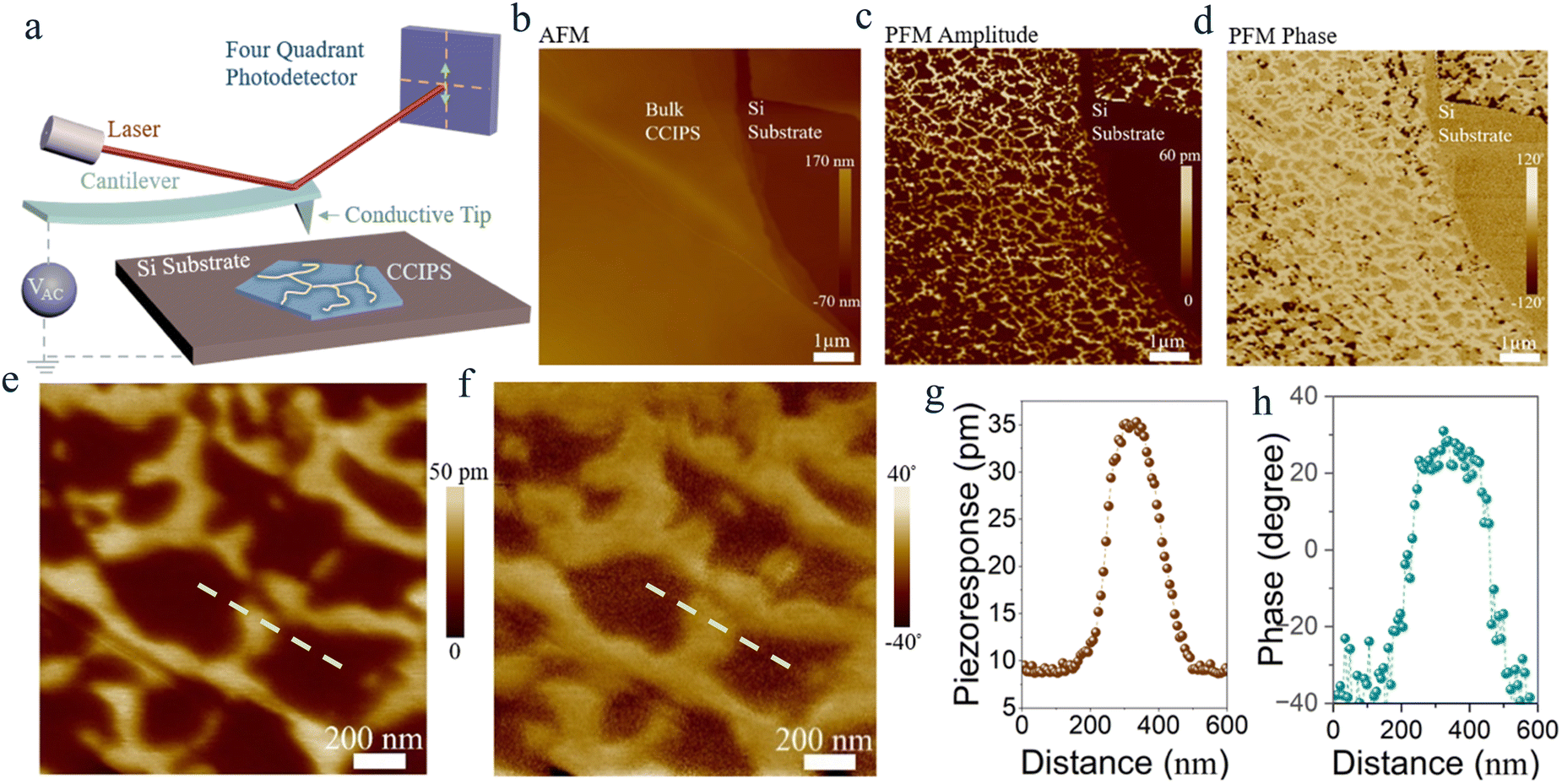 | ||
| Fig. 2 PFM imaging of piezoelectric domain walls in 2D CCIPS: (a) schematic showing the experimental configuration for PFM imaging. A conductive tip is generally used to apply the AC voltage across the sample. The green arrow on the four-quadrant photodetector indicates the out-of plane or vertical piezoelectricity measured in this project. (b) AFM topography of a bulk and multilayer CCIPS sample cleaved mechanically on a Si substrate. Sample thickness ranges from 32 nm to 90 nm. (c) and (d) Corresponding out-of-plane PFM amplitude and phase signal of the CCIPS sample, respectively showing RT vertical piezoelectricity and formation of a domain like pattern in layered CCIPS. Very little correlation between topography and piezo response is observed, indicating negligible topography cross talk in piezoelectric signal. (e) and (f) Small area out-of plane PFM amplitude and phase signals of the same sample depicting a closer view of the domain formation. (g) and (h) PFM amplitude and phase line profile signals along the green dotted line in (e) and (f), respectively. | ||
Fig. 2b shows the smooth topography of a representative CCIPS flake, indicating the preservation of high quality single crystalline structure and clean interfaces after the fabrication process. The thickness of the flake varied from 50 nm to 82 nm (Fig. S3a–c, ESI†). Fig. 2c and d show the corresponding PFM amplitude and phase images, respectively, manifesting unusual domain-like formation, with strong piezo response along the domain boundaries (see Fig. S4 (ESI†) for AFM topography, in-phase and quadrature images). These trends are observed to be independent of the topography and homogeneously distributed over the entire sample (see Fig. S5, ESI†). They have also been reproduced across different CCIPS samples with different thicknesses to ensure repeatability (Fig. S6–S8, ESI†). Small area PFM amplitude and phase signals of the sample presented in Fig. 2e and f, indicate a relatively uniform domain network, with the boundaries clearly exhibiting elevated piezo electricity by up to three-fold (Fig. 2g). Meanwhile, the PFM phase directions at the domain and domain boundaries are in different directions.
The PFM measurements are consistent with the EDS mapping results, which show the CCIPS collapsing into dual phases. Evidently, the cage-like structures (domain boundaries) incorporate higher Cu cation composition and are associated with stronger piezoelectricity. Meanwhile, the domain regions exhibit comparatively lower response. This is well correlated with their Cu deficient nature. Given that Cu is crucial for the presence of piezoelectricity in similar compounds,35,49 we suggest that the elevated piezo signal along the domain boundaries is aligned with this mechanism.
While PFM is a commonly used method for determining piezo properties of materials, it is subject to possible electrostatic, mechanical or electrochemical dipole induced artifacts.50–53 To minimize these the adverse contributions, we have used a combination of off-resonance imaging, electrostatic blind spot and substrate subtraction methods.35,51,54–60 Under these conditions, minimal electrostatic contributions or background noise was validated from the underlying Si substrate (see Fig. S9, ESI†). It has been shown that using stiffer and longer length cantilever can further reduce the electrostatic contribution in PFM measurements.55,58,59 This is because electrostatic contributions are inversely proportional to the stiffness of the cantilever and a larger tip length is known to attenuate the capacitive coupling between the tip and the surface. We have therefore validated the above results using a stiffer probe with longer cantilever length (see Methods). As shown in Fig. S10 (ESI†), similar piezo and phase contrast results are obtained from the CCIPS samples using this alternative cantilever, suggesting minimal electrostatic contribution. To further preclude electrostatic interference, and substantiate intrinsic piezoelectricity, a large reverse voltage was applied to determine if phase switching would be realized.61,62 As seen in Fig. S11 (ESI†), the phase directions in both domains and the domain boundaries are flipped under the applied negative bias voltage. These measurements suggests that the PFM results exhibit minimal electrostatic contributions and instead arise from piezoelectricity in the domains and at the domain boundaries of CCIPS.
To shed further light into the nanoscale properties of CCIPS and to confirm the preservation of piezoelectric properties, PFM scanning of bulk and multilayer flakes were conducted at progressively increasing drive voltage. By considering the slope of the measured piezo response as a function of the drive voltage, the d33 coefficient can be determined. Larger d33 coefficients indicate higher displacement and are an important parameter for piezo-MEMS components, like monitoring transducer devices.63Fig. 3a illustrates small area piezo mapping of the domains with incrementing drive voltage. 1D analysis in Fig. 3b depicts the line profiles across the domains and domain boundaries, while Fig. 3c shows the average piezo amplitude as a function of the applied voltage across the same regions. All measurements have been corrected for the instrumental noise and background contribution. A linear response for Vbias-dependance can be recorded in addition to the relatively homogenous profile. Meanwhile, a d33 coefficient of ∼6.67 pm V−1 is obtained for the domain boundary as deduced from the slope; this is more than 12-fold higher than the domain region, which divulges to a meagre ∼0.57 pm V−1 for the same quantity (Fig. 3d). Such a large elevation is a direct outcome of the enhanced piezoelectricity along the domain boundary. Notably, the consistent change of the piezoelectric signal with applied bias largely rules out any other external factors on the measured piezo response.35
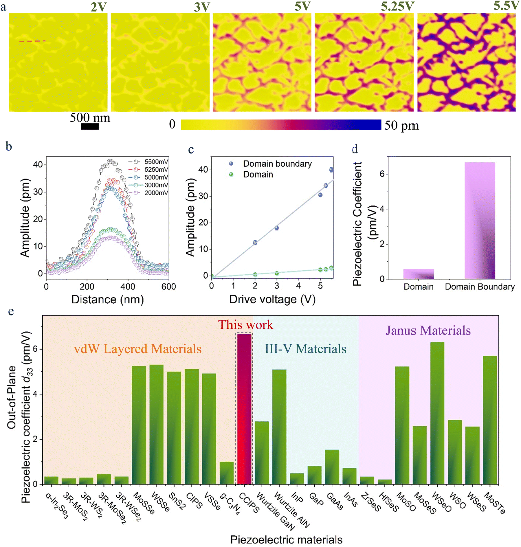 | ||
| Fig. 3 Bias dependent piezo response imaging and piezoelectric coefficient d33 of 2D CuCrInP2S6: (a) PFM amplitude images of small area (image size 1 μm × 1 μm) CuCrInP2S6 in a controlled environment. Increasing driving voltage results in gradual enhancement of the piezo amplitude causing stronger contrast. (b) PFM amplitude line profiles across the dotted line in (a), for all voltages applied. (c) Quantitative depiction of piezoelectric magnitude as a function of drive voltage for both domain and domain boundary regions. Values extracted are averaged across multiple domains and boundaries. Linear fitting is used to calculate the piezoelectric coefficient d33 from the slope. (d) Comparison of d33 for domains and domain boundaries where the latter is strikingly enhanced due to stronger piezo signal. (e) Brief summary of piezoelectric coefficients of 2D piezoelectric as obtained from literature. Y-axis represents absolute values of d33 coefficient. Note that some results are obtained from experimental PFM measurements while others are obtained from first principal calculations. These values can be found in Table S-II (ESI†). | ||
A comparison of piezoelectric coefficients of some common vdW layered materials in bulk and multilayer phases with intrinsic piezoelectricity, as well as traditional semiconductors and more recent Janus materials are included in Fig. 3e and Table S2 (ESI†). These show that the domain induced piezoelectricity in CCIPS is higher by several fold as compared to traditional bulk or multilayer TMDs, which have already envisaged ample applications. For instance, d33 coefficient in domain boundaries of CCIPS is higher by almost ∼18 and 33 times compared to conventional 3R-MoS2 and 3R-WSe2 respectively. Furthermore, in comparison to nitride and arsenide-based semiconductors and Janus materials, intrinsic piezo response in CCIPS easily surpasses these by more than an order of magnitude and even more in some cases. Such large enrichment of a pivotal component in piezoelectric materials signifies augmented sensitivity, actuation and efficiency in energy conversion. As such, the large and robust piezoelectricity of CCIPS has significant potential across multiple branches of nanoelectronics devices.25
Surface potential and harmonic generation
The stark contrast in the piezoelectric signal is strongly suggestive of a phase partition, likely comprising of Cu-rich region with enhanced piezo response. Evidently, this scenario would require a Cu-deprived region, making it mostly a non-polar dielectric or paraelectric phase, for which the piezoelectric amplitude is significantly diminished. Such ionic migration is also expected to lead to variation in surface potential since there is a direct correlation between polarization states and work function.64 This can be studied using KPFM, which is schematically represented in Fig. 4a. Fig. 4b show the measured surface potentials of the domains and domain boundaries in a CCIPS flake. Boundaries appear to experience a reduced work function due to the lower surface potential, compared to the domain regions. This is evident from the 1D analysis across a representative domain as shown in Fig. 4c. Around 30 meV variation is observed, indicating the cage-like regions with higher Cu concentrations tend to electrostatically induce negative charges. Repeatable result scan has been obtained from another bulk sample, as illustrated in Fig. S12 (ESI†). | ||
| Fig. 4 Evidence of Cu migration and phase segregation using KPFM and second harmonic mapping: (a) Schematic showing the experimental set up for KPFM measurements and a cartoon illustration of second harmonic generation. (b) KPFM map (∼3.5 μm × 3.5 μm) of CuCrInP2S6 flake showing the variation of work function across the domains and domain boundaries. (c) Line profile of surface potential across the dotted line in (b). (d) Representative SHG maps across some regions in bulk CuCrInP2S6 using 920 nm pulsed laser excitation. The domain boundaries emit significantly stronger SHG than the domains. Repetitive results have been obtained across multiple samples with different thicknesses. (e) SHG intensity line profile across the dotted lines in (f). Profiles confirm the rise in harmonic signals across the boundary regions. | ||
Piezoelectric variation in CCIPS can be further probed using second harmonic generation depicted schematically also in Fig. 4a. This technique is a second order non-linear process and occurs mostly in non-centrosymmetric media involving the emission of new photon with higher energy after two photons with lower energy and frequency are absorbed on pulsed laser excitation.31 The broken inversion symmetry of CCIPS is expected to cause a strong SHG signal, which is directly correlated with the piezoelectricity. Upon excitation with 920 nm pulsed laser, CCIPS flakes generate intense SHG signal, revealing distinct contrast between the domain and domain boundaries. The boundary regions, which are expected to be Cu-rich, have an elevated SHG of ∼40-fold compared to the domains that are Cu-poor. SHG map reveals similar cage-like domain patterns (Fig. 4d). Fig. 4e depicts an example of variation in SHG intensity using 1D line profile across a domain boundary. While SHG enhancement is not proportionate across all boundaries, it is firmly incremented compared to the domain regions. This could also be a result of associated piezoelectricity, which is elevated from the boundaries only. Fig. S13 (ESI†) manifests similar intriguing SHG response across another bulk sample, confirming the repeatability of results across the thickness of flakes investigated.
Simulations and discussion
Given the prevalence of Cu-diffusion to create multi-domain structures within CCIPS, ab initio calculations were undertaken to optimize the crystal structure and compute the energies required for Cu to overcome the hopping barrier and migrate. We first analyzed the calculated electron localization function (ELF) included in Fig. 5a, which shows that P and S atoms have localized electron clouds making it improbable for these atoms to migrate at room temperature. In contrast, Cu, Cr and In atoms have strongly delocalized electrons; thus, incrementing the probability of these atoms to migrate within the crystal lattice at RT.65 Experimental evidence indicates that ionic diffusion of Cr and In is far less likely to occur as compared to the Cu. This may partly arise from the increased ionic radius of both Cr (87 pm) and In (104 pm) compared to that of Cu (74 pm).37 | ||
| Fig. 5 DFT simulation and hopping dynamics in CCIPS: (a) Crystal structure of CCIPS revealing the electron cloud density diagram. Cyan shaded surface around phosphorus and sulphur atoms represents the ELF iso-surfaces and presence of delocalized electrons. (b) Schematic representation showing Cu ion hopping in both out-of plane and in-plane, into another possible site. EA was computed by considering an initial state (IS), final state (FS) and five different transition states (TS). Ability of Cu ion to form bond with sulphur makes it easier to migrate between the layers. (c) Kinetic barrier of the minimum energy or activation energy pathway computed from simulations for both in-plane and out-of plane Cu hopping. Y-axis represents the relative grounds state energies along the reaction coordinate and the activation barrier, EA is represented by the maximum energy from zero level. (d) Illustration of few sulphur octahedral cage depicting the possible types of sites occupied by Cu ion. Cu can have upstate or downstate in the off-centre position and migrate in multiple directions indicted by the arrows. | ||
To quantify the probability for Cu to migrate or diffuse within the crystal, the climbing image- nudge elastic band (CI-NEB) method is applied to theoretically compute the energy required by each atom to overcome the hopping barrier at RT and move between different sites. This can be modelled structurally using two layers of CCIPS and the energy barrier required for Cu to migrate across the vdW gap to an adjacent layer can be theoretically computed (see ESI† Note S1 for details). Fig. 5b schematically depicts an example of out-of-plane and in-plane movement of Cu between two hopping sites and a possible migration pathway. Fig. 5c shows the hopping barrier energy, EA, of the minimum energy pathway (MEP) for Cu atom to migrate in the respective direction, where a positive energy barrier conceives the feasibility of the process. The calculated energy barrier along the out-of-plane diffusion path is 0.42 eV, whereas the calculate energy barrier along the in-plane diffusion path is 1.4 eV. This indicates that Cu is comparatively more mobile between the 2D layers and, therefore, likely the most dominant contributor to the hopping process.
Long range dipole ordering in CCIPS is expected from the byproduct of crystal structure and atomic interactions. Cu is evidently a key contributor, with its electron density being delocalized perpendicular to the layer at RT. This can be correlated hypothetically with Cu occupying multiple possible crystallographic sites. As illustrated schematically in Fig. 5d, the three common types of partially filled sites include: (i) a quasitrigonal or an off-centre CuI; (ii) octahedral or nearly central CuII; and (iii) a tetrahedral CuIII that extends through the interlayer space or vdW gap. Given that Cu exhibits a low thermal barrier and is a highly mobile ion, this gives rise to its propensity to interchange among multiple positions, including flanking across the vdW gap due to the very low hopping barrier (Fig. 5b and c). In addition, the presence of multiple cations (Cr and In) in CCIPS can result in significant repulsive forces; causing off-centre Cu ions to potentially fill a nearby octahedral void in either direction. This leads to amplification of more similar sites in multiple sulphur cages, leading to random migration of Cu atoms from its original position along both intralayer and interlayer sites. Based on the calculated energy barriers, out-of-plane hopping is energetically more favorable due to the presence of multiple cations in the crystals lattice that can slightly impede in-plane motion. In addition, Cr occupying the interstitial sites may further resist the in-plane movement.
Recently, a similar hopping mechanism was proposed for the CIPS compound by Brehm et al.,27 who theoretically and experimentally established the presence of quadrupole wells that provide numerous potential minima, facilitating displacement of Cu ions with modest energy. Such wells were suggested to facilitate long range migration of Cu ions between the vdW gap, allowing the formation of interlayer bonds with S atoms from nearby layers.27,49 Since the CCIPS obtained in this study has evidently been synthesized with a Cu deficiency, a higher concentration of vacancies can be expected. This plays a key role in elevating the hopping motion of Cu ions into adjacent vacant octahedrons. This is further made facile due to the low energy barrier, as witnessed from DFT, and Cu–S bonds formed during the hopping motion (Fig. 5b and d) in both intralayer and interlayer directions. The higher tendency to form Cu–S bonds is made feasible due to the abundance of sulphur atoms and its ability to form six bonds per atom. Off-centre CuI ions can further yield two positions that are displaced in opposite direction from the octahedron centers,49 effectively doubling the number of hopping sites per CuS6 unit in the in-plane direction (represented by different arrows in Fig. 5d). As a result, this amplifies the possible positions Cu can occupy in both interlayer and intralayer directions. The low energy barrier further allows the hopping process between two adjacent sites in any direction to be more rapid and spontaneous. Therefore, the regular ordering of Cu atoms likely contributes to the manifestation of very uniform domain structures as witnessed in all PFM mappings, with domain sizes ranging between hundreds of nanometers to microns.
The thermal hopping motion of CuI ions between potential wells could also be a direct consequence of electron density spreading around the octahedral center. This enhances the probability of finding a copper ion at various equilibrium sites. Notably, the occupation of Cu ions in any off-center sites generates a local dipole moment which can flip between up and down states at temperatures below the transition temperature.66 These motions can take place cooperatively and lead to strong dipole correlation and a net spontaneous polarization. Freezing these motions of CuI ion would appear as static disorder or a permanent dipole. Such ordering would therefore likely induce a net piezoelectricity, as is experimentally observed here. Moreover, it would further break the inversion or two-fold symmetry, thus leading to the emission of second harmonics.66
Ionic hopping in vdW layered complex metal thiophosphates provides a dynamic platform for investigating fundamental sciences and applications based on RT piezoelectric. As such it is essential to understand the thermodynamic stability of the phase segregation. Prior quantification from TEM intensity mapping indicates that on average 3–7% Cu is possibly residing in the domain region or Cu poor area, with the remaining Cu being distributed along the domain boundaries to make them Cu rich. Fig. S14 (ESI†) shows the formation energy of CCIPS as a function of different Cu percentages (refer to Note S1 for details, ESI†). Both Cu-poor (domains) and Cu-rich (boundaries) areas appear to have stable phases and can co-exist. However, if Cu is completely removed, the structure becomes unstable, which explains the presence of small amounts of Cu in the domain region as evidenced through TEM elemental mapping.
To gain an insight on the charge neutrality, the oxidation state of the elements in the compound was manifested from X-ray photoelectron spectroscopy (XPS) measurements (see Fig. S15 and Note S2, ESI†) and Bader charge analysis (Fig. S16 and Note S1, ESI†). The Bader charge of the chromium site changes from 1.0e to 0.7e, implying that the Cr can attain different oxidation states in the complex CCIPS crystal lattice. The change in oxidation state of Cr-atoms can be geometrically substantiated by simultaneous elongation and contraction of the Cr–S bonds throughout the lattice structure (Fig. S16, ESI†). The Cr–S bond valence sum (BVS)67 calculated for each Cr-atom, reveals the co-existence of multiple oxidation state of Cr on account of different Cr–S bond distances, which is manifested through variable Bader charge transfer between Cr and S atoms. Thus, Cu-deficiency and a variable oxidation state of Cr-atoms in the complex CCIPS structure aid to maintain charge neutrality as well as stabilize the structure thermodynamically.
Conclusion
We have unambiguously established the existence of cage-like domain structures in vdW layered Cu-deficient CuCrInP2S6 at room temperature using quantitative piezoelectric imaging. Such domain structures enable for a significantly elevated piezo amplitude along their boundaries, as well as an enhanced d33 coefficient. The domain structures also reveal variations in surface potential with an upsurge in second harmonic emission. The results are substantiated with elemental mappings, clearly distinguishing Cu-rich and Cu-poor regions contributing to these phenomena. DFT simulations and ab initio studies suggest that ion migration of Cu ions facilitates this spatial copper segregation. Specifically, the ability of Cu atoms to occupy octahedral voids along both interlayer and intralayer directions through bond formation with sulphur atoms was identified as a key driver behind such nanoscale composition dynamics. The promising ferroic properties revealed here of vdW layered CuCrInP2S6, indicate that this is an interesting candidate for multifarious optoelectronic devices, including sensors and energy harvesters. This work provides the genesis towards considering how complex vdW materials stimulate the formation of novel physics and functional components in piezoelectrics.Methods
Sample fabrication
2D flakes of CCIPS were fabricated by the well-proven mechanical exfoliation methods.45,68 Heavily doped Si wafers or substrates were first cut into 10 × 10 mm2-size chips which was followed by thorough cleaning in ultrasonic bath of acetone, IPA and DI water. CCIPS crystals grown using flux zone growth technique were obtained commercially from 2D semiconductors and exfoliated using the Scotch tape method. CCIPS tapes were directly bought in contact with PDMS or gel films to obtain the exfoliated samples. Flakes were identified by an ultrahigh resolution optical microscope system from Olympus. Bulk and multilayer flakes can be easily identified based on optical contrast. These were then transferred to pre-washed Si substrates using vdW transfer method69 for further characterization. All samples used in this project are derived from one bulk crystal obtained commercially from a single batch.SEM, TEM and EDX characterization
Scanning electron microscope couple to energy dispersive X-ray spectroscopic analysis was performed using a field emission scanning electron microscope (FEI Quanta 3D FIB SEM) equipped with a EDAX Pegasus and TEAM X-ray analysis system as well as 10 mm2 SDD with ultra-thin window. The samples on Si substrate were mounted on to a SEM sample holder using double-sided sticky carbon tape. No additional coatings were applied to the SEM samples as the sample are conductive. STEM images and EDS analysis were obtained using an FEI Tecnai G2 F20 S-TWIN TEM equipped with a Bruker X-Flash X-ray detector.XRD, XPS and Raman spectroscopy
XRD data was collected with a Bruker D8 ADVANCE diffractometer [Cu-kα (λ = 0.15406 nm) radiation], with the 1600 W Cu-anode coupled with Ni-filters. The measurement was conducted in an ambient environment using Anton-Paar HTK 1200 N chamber.X-Ray photoelectron spectroscopy was carried out using Nexsa, Thermo Fisher Scientific. Al Kα and He(I) sources (21.21 eV) with a pass energy of 200 eV (50 eV for a narrow scan) and 3 eV were used to emit X-ray and UV photons, respectively. The measurement was conducted with a chamber pressure below 5.0 × 10⁻⁸ Torr. The XPS narrow scan line profile was decomposed into peaks fitted using Gaussian (70%) and Lorentzian (30%). The Shirley function was used for background correction. Data were analyzed using Avantage software. Binding energies were corrected to the aliphatic C 1s peak at 284.8 eV, and the intensity of the spectra were normalized to the same peak.
Raman measurements were conducted using Confocal Microscope System (Witec Alpha 300R) with a 100× objective lens (NA = 0.9) in ambient condition. A fiber coupled 532 nm CW laser having a spot size of 1 μm diameter was used as excitation source. The samples were illuminated from the top side on a piezo-crystal-controlled scanning stage.
PFM and KPFM microscopy
PFM imaging and measurements as well as KPFM characterization were performed on Dimension Icon Microscope with Nanoscope VI controller from Bruker Technologies in a class 10![[thin space (1/6-em)]](https://www.rsc.org/images/entities/char_2009.gif) 000 clean room setup. SCM-PIT-V2 (Bruker) platinum–iridium coated tip with a spring constant of 3 N m−1 and tip end radius of 25 nm was used for all PFM measurements. AC bias was applied through the tip, and induced sample deformation whose amplitude and phase represent the magnitude of the piezoelectric coefficient and the polarization direction of the response, was detected respectively. It was driven under an AC bias voltage in the range of VAC = 2–5.5 V and frequencies were around 230–250 KHz. In order to avoid mixing of mechanical response with piezoelectric response, measurements were performed in off-resonance mode. To avoid drifting of the contact resonance frequency due to mechanical changes, contact resonance frequency sweeps were performed before every scan to recalibrate to sub-contact resonance frequency. For d33 quantification, a relatively small and optimal drive voltages were used to achieve good signal-noise ratio and to avoid polarization switching and non-linearity effect. For stiffer cantilever Bruker DDESP-FM-V2 probe with k = 6 N m−1 was used for further validating the results.
000 clean room setup. SCM-PIT-V2 (Bruker) platinum–iridium coated tip with a spring constant of 3 N m−1 and tip end radius of 25 nm was used for all PFM measurements. AC bias was applied through the tip, and induced sample deformation whose amplitude and phase represent the magnitude of the piezoelectric coefficient and the polarization direction of the response, was detected respectively. It was driven under an AC bias voltage in the range of VAC = 2–5.5 V and frequencies were around 230–250 KHz. In order to avoid mixing of mechanical response with piezoelectric response, measurements were performed in off-resonance mode. To avoid drifting of the contact resonance frequency due to mechanical changes, contact resonance frequency sweeps were performed before every scan to recalibrate to sub-contact resonance frequency. For d33 quantification, a relatively small and optimal drive voltages were used to achieve good signal-noise ratio and to avoid polarization switching and non-linearity effect. For stiffer cantilever Bruker DDESP-FM-V2 probe with k = 6 N m−1 was used for further validating the results.
Two pass KPFM was performed in AM-KPFM mode. First pass acquires the sample topography in the tapping mode while probe is grounded. Consequently, the probe is lifted to a constant height and scanned in line with samples topography. During the second pass, an a.c voltage, Va.c is applied to the probe that creates an oscillating electrostatic force. This is further minimized through an additional D.C voltage which is essentially equivalent to the contact potential difference between the tip and sample. Eventually the local work function for the sample or the surface can be extracted using a tip with a known material. KPFM measurements were optimized against both the applied A.C voltage and lift height. All measurements were repeated multiple times to obtain consistent output and ensure reliability.
Second harmonic generation spectroscopy
Images were acquired with Leica SP8 confocal microscope on the upright DM6000 stand with a dry HCX PL FLUOTAR CORR PH2 40×/0.6 objective. Spectra-Physics Mai Tai HP infra-red pulsed laser tuned to 920 nm was used as an excitation source. Back-scattered second harmonic generation (SHG) signal was detected by a non-descanned (NDD) hybrid detector (HyD) with a narrow Semrock 460/14 band-pass filter.Data availability
The data that support the findings of this study are available within the article and its ESI.†Conflicts of interest
Authors declare no conflict of interest.Acknowledgements
J. J. acknowledges financially the Australia Research Council funded Centre of Excellence in Exciton Science (CE170100026) and Discovery Project scheme (DP220103783). This work was performed in part at the Melbourne Centre for Nanofabrication (MCN) in the Victorian Node of the Australian National Fabrication Facility (ANFF). The work was also supported by the Australian Renewable Energy Agency funded Australian Centre for Advanced Photovoltaics (ACAP). S. R. acknowledge the use of the instruments at the Monash Centre for Electron Microscopy, a Node of Microscopy Australia. S. R. acknowledge the use of the facilities at the Monash X-ray Platform and Monash Micro Imaging for facility support. A. A. acknowledges computing facility (spacetime2) provided by IIT Bombay to support this research. S. P. acknowledges the computational support by MASSIVE HPC facility (https://www.massive.org.au) and the Monash eResearch Centre and eSolutions-Research Support Services through the use of the MonARCH HPC Cluster.References
- A. K. Geim and K. S. Novoselov, The rise of graphene, Nat. Mater., 2007, 6, 183–191, DOI:10.1038/nmat1849.
- A. Gupta, T. Sakthivel and S. Seal, Recent development in 2D materials beyond graphene, Prog. Mater. Sci., 2015, 73, 44–126, DOI:10.1016/j.pmatsci.2015.02.002.
- V. Shanmugam, et al., A Review of the Synthesis, Properties, and Applications of 2D Materials, Part. Part. Syst. Charact., 2022, 39, 2200031, DOI:10.1002/ppsc.202200031.
- A. K. Geim and I. V. Grigorieva, van der Waals heterostructures, Nature, 2013, 499, 419–425, DOI:10.1038/nature12385.
- S. Z. Butler, et al., Progress, Challenges, and Opportunities in Two-Dimensional Materials Beyond Graphene, ACS Nano, 2013, 7, 2898–2926, DOI:10.1021/nn400280c.
- Y. Pinki, S. Dewan, R. Mishra and S. Das, Review of recent progress, challenges, and prospects of 2D materials-based short wavelength infrared photodetectors, J. Phys. D: Appl. Phys., 2022, 55, 313001, DOI:10.1088/1361-6463/ac6635.
- M. Malik, M. A. Iqbal, J. R. Choi and P. V. Pham, 2D Materials for Efficient Photodetection: Overview, Mechanisms, Performance and UV-IR Range Applications, Front. Chem., 2022, 10, 905404, DOI:10.3389/fchem.2022.905404.
- S. Das, D. Pandey, J. Thomas and T. Roy, The Role of Graphene and Other 2D Materials in Solar Photovoltaics, Adv. Mater., 2019, 31, 1802722, DOI:10.1002/adma.201802722.
- U. K. Aryal, et al., 2D materials for organic and perovskite photovoltaics, Nano Energy, 2022, 94, 106833, DOI:10.1016/j.nanoen.2021.106833.
- S. Ren, Q. Tan and J. Zhang, Review on the quantum emitters in two-dimensional materials, J. Semicond., 2019, 40, 071903, DOI:10.1088/1674-4926/40/7/071903.
- M. M. Rehman, et al., Decade of 2D-materials-based RRAM devices: a review, Sci. Technol. Adv. Mater., 2020, 21, 147–186, DOI:10.1080/14686996.2020.1730236.
- L. Yin, R. Cheng, Y. Wen, C. Liu and J. He, Emerging 2D Memory Devices for In-Memory Computing, Adv. Mater., 2021, 33, 2007081, DOI:10.1002/adma.202007081.
- E. C. Ahn, 2D materials for spintronic devices, npj 2D Mater. Appl., 2020, 4, 17, DOI:10.1038/s41699-020-0152-0.
- K. S. Novoselov, et al., Electric Field Effect in Atomically Thin Carbon Films, Science, 2004, 306, 666–669, DOI:10.1126/science.1102896.
- Q. H. Wang, K. Kalantar-Zadeh, A. Kis, J. N. Coleman and M. S. Strano, Electronics and optoelectronics of two-dimensional transition metal dichalcogenides, Nat. Nanotechnol., 2012, 7, 699–712, DOI:10.1038/nnano.2012.193.
- M. Chhowalla, et al., The chemistry of two-dimensional layered transition metal dichalcogenide nanosheets, Nat. Chem., 2013, 5, 263–275, DOI:10.1038/nchem.1589.
- S. Qian, X. Wang and W. Yan, Piezoelectric fibers for flexible and wearable electronics, Front. Optoelectron., 2023, 16, 3, DOI:10.1007/s12200-023-00058-3.
- A. Bolotsky, et al., Two-Dimensional Materials in Biosensing and Healthcare: From In Vitro Diagnostics to Optogenetics and Beyond, ACS Nano, 2019, 13, 9781–9810, DOI:10.1021/acsnano.9b03632.
- A. Kausar, I. Ahmad, M. H. Eisa and M. Maaza, Graphene Nanocomposites in Space Sector—Fundamentals and Advancements, C, 2023, 9, 29 Search PubMed.
- A. Wali and S. Das, Hardware and Information Security Primitives Based on 2D Materials and Devices, Adv. Mater., 2023, 35, 2205365, DOI:10.1002/adma.202205365.
- Y. Wu, Y. Ma, H. Zheng and S. Ramakrishna, Piezoelectric materials for flexible and wearable electronics: A review, Mater. Des., 2021, 211, 110164, DOI:10.1016/j.matdes.2021.110164.
- S. C. Masmanidis, et al., Multifunctional Nanomechanical Systems via Tunably Coupled Piezoelectric Actuation, Science, 2007, 317, 780–783, DOI:10.1126/science.1144793.
- Z. L. Wang and J. Song, Piezoelectric Nanogenerators Based on Zinc Oxide Nanowire Arrays, Science, 2006, 312, 242–246, DOI:10.1126/science.1124005.
- W. Wu, et al., Piezoelectricity of single-atomic-layer MoS2 for energy conversion and piezotronics, Nature, 2014, 514, 470–474, DOI:10.1038/nature13792.
- S. K. Ghosh and D. Mandal in 2D Nanomaterials for Energy Applications, ed. S. Zafeiratos, Elsevier, 2020, pp. 1–38 Search PubMed.
- M. A. Susner, M. Chyasnavichyus, M. A. McGuire, P. Ganesh and P. Maksymovych, Metal Thio- and Selenophosphates as Multifunctional van der Waals Layered Materials, Adv. Mater., 2017, 29, 1602852, DOI:10.1002/adma.201602852.
- J. A. Brehm, et al., Tunable quadruple-well ferroelectric van der Waals crystals, Nat. Mater., 2020, 19, 43–48, DOI:10.1038/s41563-019-0532-z.
- V. Maisonneuve, et al., Ionic conductivity in ferroic CuInP2S6 and CuCrP2S6, Ferroelectrics, 1997, 196, 257–260 Search PubMed.
- F. Liu, et al., Room-temperature ferroelectricity in CuInP2S6 ultrathin flakes, Nat. Commun., 2016, 7, 12357, DOI:10.1038/ncomms12357.
- X. Wang, et al., van der Waals engineering of ferroelectric heterostructures for long-retention memory, Nat. Commun., 2021, 12, 1109, DOI:10.1038/s41467-021-21320-2.
- S. Rahman, T. Yildirim, M. Tebyetekerwa, A. R. Khan and Y. Lu, Extraordinary Nonlinear Optical Interaction from Strained Nanostructures in van der Waals CuInP2S6, ACS Nano, 2022, 16, 13959–13968, DOI:10.1021/acsnano.2c03294.
- M. A. Susner, R. Rao, A. T. Pelton, M. V. McLeod and B. Maruyama, Temperature-dependent Raman scattering and x-ray diffraction study of phase transitions in layered multiferroic CuCr P2S6, Phys. Rev. Mater., 2020, 4, 104003, DOI:10.1103/PhysRevMaterials.4.104003.
- A. J. Healey, et al., Varied Magnetic Phases in a van der Waals Easy-Plane Antiferromagnet Revealed by Nitrogen-Vacancy Center Microscopy, ACS Nano, 2022, 16, 12580–12589, DOI:10.1021/acsnano.2c04132.
- W. F. Io, et al., Direct observation of intrinsic room-temperature ferroelectricity in 2D layered CuCrP2S6, Nat. Commun., 2023, 14, 7304, DOI:10.1038/s41467-023-43097-2.
- A. Dziaugys, et al., Piezoelectric domain walls in van der Waals antiferroelectric CuInP2Se6, Nat. Commun., 2020, 11, 3623, DOI:10.1038/s41467-020-17137-0.
- W. Kleemann, V. V. Shvartsman, P. Borisov, J. Banys and Y. M. Vysochanskii, Magnetic and polar phases and dynamical clustering in multiferroic layered solid solutions CuCr1−xInxP2S6, Phys. Rev. B:Condens. Matter Mater. Phys., 2011, 84, 094411, DOI:10.1103/PhysRevB.84.094411.
- Q. He, et al., Antisite defects in layered multiferroic CuCr0.9In0.1P2S6, Nanoscale, 2015, 7, 18579–18583, 10.1039/C5NR04779J.
- J. Tan, et al., Large out-of-plane piezoelectricity of oxygen functionalized MXenes for ultrathin piezoelectric cantilevers and diaphragms, Nano Energy, 2019, 65, 104058, DOI:10.1016/j.nanoen.2019.104058.
- X. Jiang, et al., Manipulation of current rectification in van der Waals ferroionic CuInP2S6, Nat. Commun., 2022, 13, 574, DOI:10.1038/s41467-022-28235-6.
- R. Rao, et al., Investigating Strain between Phase-Segregated Domains in Cu-Deficient CuInP2S6, Chem. Mater., 2023, 35, 8020–8029, DOI:10.1021/acs.chemmater.3c01238.
- R. Rao, R. Selhorst, B. S. Conner and M. A. Susner, Ferrielectric-paraelectric phase transitions in layered CuInP2S6 and CuInP2S6-In4/3P2S6 heterostructures: A Raman spectroscopy and x-ray diffraction study, Phys. Rev. Mater., 2022, 6, 045001, DOI:10.1103/PhysRevMaterials.6.045001.
- W. Yang, et al., Highly tunable Raman scattering and transport in layered magnetic Cr2S3 nanoplates grown by sulfurization, 2D Mater., 2019, 6, 035029, DOI:10.1088/2053-1583/ab1bc0.
- S. Zhou, et al., Ultrathin Non-van der Waals Magnetic Rhombohedral Cr2S3: Space-Confined Chemical Vapor Deposition Synthesis and Raman Scattering Investigation, Adv. Funct. Mater., 2019, 29, 1805880, DOI:10.1002/adfm.201805880.
- R. Rao and M. A. Susner, Phonon anharmonicity in Cu-based layered thiophosphates, Mater. Today Commun., 2023, 35, 105840, DOI:10.1016/j.mtcomm.2023.105840.
- S. Rahman, B. Liu, B. Wang, Y. Tang and Y. Lu, Giant Photoluminescence Enhancement and Resonant Charge Transfer in Atomically Thin Two-Dimensional Cr2Ge2Te6/WS2 Heterostructures, ACS Appl. Mater. Interfaces, 2021, 13, 7423–7433, DOI:10.1021/acsami.0c20110.
- M. A. Susner, et al., Cation–Eutectic Transition via Sublattice Melting in CuInP2S6/In4/3P2S6 van der Waals Layered Crystals, ACS Nano, 2017, 11, 7060–7073, DOI:10.1021/acsnano.7b02695.
- N. Balke, et al., Exploring Local Electrostatic Effects with Scanning Probe Microscopy: Implications for Piezoresponse Force Microscopy and Triboelectricity, ACS Nano, 2014, 8, 10229–10236, DOI:10.1021/nn505176a.
- H. Röhm, T. Leonhard, M. J. Hoffmann and A. Colsmann, Ferroelectric Poling of Methylammonium Lead Iodide Thin Films, Adv. Funct. Mater., 2020, 30, 1908657, DOI:10.1002/adfm.201908657.
- D. Zhang, et al., Anisotropic Ion Migration and Electronic Conduction in van der Waals Ferroelectric CuInP2S6, Nano Lett., 2021, 21, 995–1002, DOI:10.1021/acs.nanolett.0c04023.
- F. Xue, et al., Multidirection Piezoelectricity in Mono- and Multilayered Hexagonal α-In2Se3, ACS Nano, 2018, 12, 4976–4983, DOI:10.1021/acsnano.8b02152.
- S. Yuan, et al., A Giant Tunable Piezoelectric Performance in Two-dimensional In2Se3 via Interface Engineering, Adv. Electron. Mater., 2024, 10, 2300741, DOI:10.1002/aelm.202300741.
- D. Seol, B. Kim and Y. Kim, Non-piezoelectric effects in piezoresponse force microscopy, Curr. Appl. Phys., 2017, 17, 661–674, DOI:10.1016/j.cap.2016.12.012.
- G. Alosaimi, C.-Y. Huang, P. Sharma, T. Wu and J. Seidel, Morphology-Dependent Charge Carrier Dynamics and Ion Migration Behavior of CsPbBr3 Halide Perovskite Quantum Dot Films, Small, 2023, 19, 2207220, DOI:10.1002/smll.202207220.
- A. Garduño-Medina, M. A. Vázquez-Delgado, C. J. Diliegros-Godines, V. García-Vázquez and F. J. Flores-Ruiz, Measurements outside resonance with piezoresponse force microscopy, AIP Conf. Proc., 2021, 2416, 020010, DOI:10.1063/5.0068705.
- A. Gomez, T. Puig and X. Obradors, Diminish electrostatic in piezoresponse force microscopy through longer or ultra-stiff tips, Appl. Surf. Sci., 2018, 439, 577–582, DOI:10.1016/j.apsusc.2018.01.080.
- X. Jiang, et al., Strong Piezoelectricity and Improved Rectifier Properties in Mono- and Multilayered CuInP2S6, Adv. Funct. Mater., 2023, 33, 2213561, DOI:10.1002/adfm.202213561.
- J. P. Killgore, L. Robins and L. Collins, Electrostatically-blind quantitative piezoresponse force microscopy free of distributed-force artifacts, Nanoscale Adv., 2022, 4, 2036–2045, 10.1039/D2NA00046F.
- S. Kim, D. Seol, X. Lu, M. Alexe and Y. Kim, Electrostatic-free piezoresponse force microscopy, Sci. Rep., 2017, 7, 41657, DOI:10.1038/srep41657.
- R. Proksch, In-situ piezoresponse force microscopy cantilever mode shape profiling, J. Appl. Phys., 2015, 118, 072011, DOI:10.1063/1.4927809.
- T.-H.-Y. Vu, D. Bennett, G. N. Pallewella, M. H. Uddin, K. Xing, W. Zhao, S. H. Lee, Z. Mao, J. B. Muir, L. Jia, J. A. Davis, K. Watanabe, T. Taniguchi, S. Adam, P. Sharma, M. S. Fuhrer and M. T. Edmonds, Imaging topological polar structures in marginally twisted 2D semiconductors, Archive, 2024, preprint, arXiv:2405.15126 DOI:10.48550/arXiv.2405.15126.
- G. Pica, et al., Photo-ferroelectric perovskite interfaces for boosting VOC in efficient perovskite solar cells, Nat. Commun., 2024, 15, 8753, DOI:10.1038/s41467-024-53121-8.
- P. Sharma, et al., A room-temperature ferroelectric semimetal, Sci. Adv., 2019, 5, eaax5080, DOI:10.1126/sciadv.aax5080.
- S. Rana, V. Singh and B. Singh, Recent trends in 2D materials and their polymer composites for effectively harnessing mechanical energy, iScience, 2022, 25, 103748, DOI:10.1016/j.isci.2022.103748.
- N. Barrett, et al., Influence of the ferroelectric polarization on the electronic structure of BaTiO3 thin films, Surf. Interface Anal., 2010, 42, 1690–1694, DOI:10.1002/sia.3369.
- L. Zhu, Q.-M. Hu and R. Yang, The effect of electron localization on the electronic structure and migration barrier of oxygen vacancies in rutile, J. Phys.: Condens. Matter, 2014, 26, 055602, DOI:10.1088/0953-8984/26/5/055602.
- V. B. Cajipea, et al., Copper ordering in lamellar CuMP2S6 (M = Cr, In): Transition to an antiferroelectric or ferroelectric phase, Ferroelectrics, 1996, 185, 135–138, DOI:10.1080/00150199608210497.
- R. M. Wood and G. J. Palenik, Bond Valence Sums in Coordination Chemistry. A Simple Method for Calculating the Oxidation State of Cobalt in Complexes Containing Only Co−O Bonds, Inorg. Chem., 1998, 37, 4149–4151, DOI:10.1021/ic980176q.
- Y. Huang, et al., Reliable Exfoliation of Large-Area High-Quality Flakes of Graphene and Other Two-Dimensional Materials, ACS Nano, 2015, 9, 10612–10620, DOI:10.1021/acsnano.5b04258.
- S. Rahman, X. Sun, Y. Zhu and Y. Lu, Extraordinary Phonon Displacement and Giant Resonance Raman Enhancement in WSe2/WS2 Moiré Heterostructures, ACS Nano, 2022, 16, 21505–21517, DOI:10.1021/acsnano.2c10092.
Footnote |
| † Electronic supplementary information (ESI) available. See DOI: https://doi.org/10.1039/d4nh00580e |
| This journal is © The Royal Society of Chemistry 2025 |