
 Open Access Article
 This Open Access Article is licensed under a
 Creative Commons Attribution 3.0 Unported Licence
Forming and compliance-free operation of low-energy, fast-switching HfOxSy/HfS2 memristors†
Aferdita
Xhameni
 ab,
AbdulAziz
AlMutairi
ac,
Xuyun
Guo
d,
Irina
Chircă
c,
Tianyi
Wen
b,
Stephan
Hofmann
c,
Valeria
Nicolosi
d and
Antonio
Lombardo
*ab
ab,
AbdulAziz
AlMutairi
ac,
Xuyun
Guo
d,
Irina
Chircă
c,
Tianyi
Wen
b,
Stephan
Hofmann
c,
Valeria
Nicolosi
d and
Antonio
Lombardo
*ab
aLondon Centre for Nanotechnology, 19 Gordon St, London, WC1H 0AH, UK. E-mail: a.lombardo@ucl.ac.uk
bDepartment of Electronic & Electrical Engineering, Malet Place, University College London, WC1E 7JE, UK
cDepartment of Engineering, University of Cambridge, Cambridge, CB3 0FA, UK
dSchool of Chemistry, Centre for Research on Adaptive Nanostructures and Nanodevices (CRANN) & Advanced Materials Bio-Engineering Research Centre (AMBER), Trinity College Dublin, Dublin 2, Ireland
First published on 15th January 2025
Abstract
We demonstrate low energy, forming and compliance-free operation of a resistive memory obtained by the partial oxidation of a two-dimensional layered van-der-Waals semiconductor: hafnium disulfide (HfS2). Semiconductor–oxide heterostructures are achieved by low temperature (<300 °C) thermal oxidation of HfS2 under dry conditions, carefully controlling process parameters. The resulting HfOxSy/HfS2 heterostructures are integrated between metal contacts, forming vertical crossbar devices. Forming-free, compliance-free resistive switching between non-volatile states is demonstrated by applying voltage pulses and measuring the current response in time. We show non-volatile memory operation with an RON/ROFF of 102, programmable by 80 ns WRITE and ERASE operations. Multiple stable resistance states are achieved by modulating pulse width and amplitude, down to 60 ns, < 20 pJ operation. This demonstrates the capability of these devices for low-energy, fast-switching and multi-state programming. Resistance states were retained without fail at 150 °C over 104 s, showcasing the potential of these devices for long retention times and resilience to ageing. Low-energy resistive switching measurements were repeated under vacuum (8.6 mbar) showing unchanged characteristics and no dependence of the device on surrounding oxygen or water vapour. Using a technology computer-aided design (TCAD) tool, we explore the role of the semiconductor layer in tuning the device conductance and driving gradual resistive switching in 2D HfOx-based devices.
New conceptsWe employ a low-temperature, dry oxidation method to partially convert an HfS2 crystal to a vertical HfOxSy/HfS2 structure. As opposed to most other works on oxidation-conversion of 2D semiconductors, our process results in a thin, highly crystalline oxide–semiconductor heterostructure with almost perfect interfaces. Crossbar-arrays of amorphous oxide-based memristors typically require peripheral circuitry to enable electroforming (a one-time process required to initialise the devices) and current compliance circuitry (to limit high currents which may damage the devices). Both of these requirements hinder energy consumption, computation time and integration density in machine learning and neuromorphic applications. Devices which exhibit forming-free and compliance-free operation have been investigated previously; however, they typically exhibit resistive switching with a low ON/OFF ratio and/or require fabrication processes which are incompatible with CMOS. By using thermally-grown HfOxSy/HfS2 structures, we demonstrate electroforming-free and compliance-free, non-volatile resistive switching while maintaining a good ON/OFF ratio and a CMOS-compatible thermal budget. Our devices also show multiple resistive states, as well as stability at high temperatures and under vacuum. Using TCAD simulations, we demonstrate that the HfS2 semiconducting layer enables the engineering of ON currents. We also show that the mechanism responsible for the forming-free and compliance-free resistive switching in the device is non-filamentary, unlike most oxide-based memristors. |
Introduction
The growing demand for data-driven computation in artificial intelligence (AI) and machine learning (ML) applications has skyrocketed energy consumption from modern data centres, with estimates showing that global yearly usage from this sector surpasses 200 TW-hours per year. This figure is predicted to rise by an order of magnitude by 20301 highlighting the growing need to address this problem.2 One fundamental issue lies in the von Neumann architecture used for computation, which physically separates processing and memory units. The shuttling of data back and forth between such processing and memory units inevitably wastes energy and increases computation time. Neuromorphic computing aims to address this by taking inspiration from the human brain–a biological “computer” capable of performing complex tasks with far higher efficiency. For example, Google DeepMind's AlphaGo model requires the use of 1920 CPUs and 280 GPUs and consumes ∼1 MW power to play the boardgame Go (inference) against a human player. Comparatively, the human brain uses only ∼20 W for the same task.3,4 One feature of the brain directly responsible for this discrepancy is the co-location of processing and memory in an extensive network of neurons and synapses. In combination with other factors, this means that handling noisy and unstructured data is a relatively unremarkable task for the human brain, enabling us to quickly, reliably and efficiently tackle complex problems. Even when handled by the best artificial neural networks (ANN) running on modern hardware, most ML and AI implementations require extensive and costly training, consume large amounts of power and require frequent retraining.5 Therefore, it is clear that for computing tasks which benefit from quick and efficient processing of noisy input data, brain-like (neuromorphic) computation is necessary.6To implement neuromorphic computations, we can take inspiration from the brain and develop systems which allow computations in memory. A common approach is to use crossbar arrays of densely-packed non-volatile memory (NVM) devices in deep neural networks (DNN) or spiking neural networks (SNN).7 Usually, the NVM devices forming the building blocks of crossbar arrays are memristors. Memristors are two-terminal, non-linear devices with inherent memory and represent a leading candidate for hardware implementations of neuromorphic computing.8 They have the ability to modulate their resistance between distinct states by the application of electrical stress, such as ramped or pulsed voltages. Crucially, they retain their programmed resistance even when the electrical stress is removed.9
Non-volatile resistive switching in solid-state devices based on titanium oxide thin films has been observed as early as 1960,10 with the memristor first being formally described in 1971 by Leon Chua.9 More recent interest in ReRAM memristive technology was sparked in 2008 when devices based on thin titanium oxide films were once again investigated, this time directly addressing Chua's memristor framework,11 and later when memristors were integrated in silicon suboxide films.12 Since then, the field has flourished, with improvements in our understanding of the switching mechanisms of ReRAM devices,13,14 the performance of each individual element,15–17 scaling18–20 and different material systems. One particular material that we will investigate is hafnium oxide (HfOx), sometimes referred to as hafnia. Hafnium oxide is part of a class of materials called high-k dielectrics. High-k dielectrics are so named as they possess a high dielectric constant compared to SiO2, which allows the use of thicker layers in metal oxide semiconductor (MOS) capacitors to suppress tunnelling while maintaining large capacitance.21 In memristive applications HfOx-based devices fabricated by sputtering or atomic layer deposition (ALD) have already demonstrated low-energy switching, a high degree of scalability, signal processing, image compression and convolutional filtering,22 good endurance23 and synaptic applications24,25 although there has been a collective desire to increase programming linearity in synaptic applications and reduce the individual memristor power consumption.26 One potential avenue of investigation for fabricating low-power memristors is to look at 2D layered materials (2DLMs).
Since the ground-breaking experiment where single layers of graphene were isolated and their electron transport was investigated,27 several more 2DLMs have been discovered with thousands more predicted to exist.28 They often have unique properties which highlight a key interest in their research. In particular, 2DLMs present the opportunity to fabricate devices with atomic precision of thicknesses down to a single atomic layer, with chemically abrupt surfaces and no dangling bonds.17,29–33 This allows devices with a wide range of properties and applications to be realised, combining different materials with varying properties with ease.33 Wafer-scale growth of desired 2DLMs for memristors by chemical vapour deposition (CVD) has been developed,19 with pilot lines already established. For example, memristors fabricated from wafer-scale CVD hexagonal boron nitride (hBN) have shown both a high ON/OFF ratio of 1011 and energy consumption as low as 8.8 zJ, demonstrating the potential of this technology.29,34 However, sample-to-sample variation and poor control of defect densities present in the films make them as-yet unsuitable for at-scale fabrication of memristors.35 Another scalable fabrication technique that has been demonstrated with 2D materials of particular interest is the template growth of ultrathin oxides from semiconducting crystals. Starting from a near-perfect crystalline 2DLM, native oxides can be formed by partially oxidising semiconducting crystals with almost perfect interfaces, using plasma oxidation,36–38 thermal oxidation39 or photo-oxidation.40 Native oxides obtained by plasma oxidation of a starting 2D crystal have shown promising memristive behaviour in work done on GaS36 and HfSe237 memristors. Recently, GaSxOy/GaS memristors with an ultrathin oxide and a clean interface have been demonstrated, showing low energy ∼0.22 nJ operation.36 Similarly, plasma oxidised HfOxSey/HfSe2 memristors have also been fabricated, demonstrating operation at low current compliance (100 pA) and low energy (0.1 fJ) in filamentary resistance switching.37
Despite the excellent performance being demonstrated in many memristors, devices which can be operated without the requirement for compliance or electroforming are even more desirable to reduce the power consumption, operation time and integration area cost of utilising memristors as synaptic weights in neuromorphic chips, improving efficiency.41 The peripheral circuitry and transistor-memristor (1T1M) architectures required to integrate most ReRAM memristors into neuromorphic and ML chips provide a high barrier to their adoption.41,42 A few fabrication methods have shown promise in this regard. Methods which engineer a large proportion of oxygen vacancies in the pristine device such as H2 annealing or using a Ti electrode gettering layer have been largely successful in promoting forming-free behaviour in ZnO42 and Ta2O5 memristors,43 respectively. However, the highly defective oxide switching layers inducing forming-free resistive switching also necessitate the application of current compliance to prevent high currents from damaging the device.42,43 SnOx ReRAM devices have been shown to exhibit both forming and compliance-free resistive switching. The forming-free behaviour is thought to be due to the ultra-thin oxide used41 and the compliance-free nature of this device is thought to be a result of the TiO2−x interfacial layer acting as a series resistor, limiting currents and driving gradual resistive switching. However, devices which exhibit forming and compliance-free or gradual switching properties typically show a low RON/ROFF,41,44 or employ fabrication techniques incompatible with CMOS.45,46
This presents a technological challenge: to fabricate devices which can combine strong non-volatile memory characteristics such as resistive switching at low energy and stable retention (found in many abrupt switching devices), while allowing for nearly continuous multi-level switching, high integration density and simplified operation without electroforming or compliance (which can be found in many gradual switching devices.) In this work, we address this by investigating the use of HfOxSy/HfS2 structures where a thin HfOxSy oxide is obtained by partial oxidation of 2D HfS2 crystals for resistive memories. The oxidation of HfS2 flakes has already been demonstrated by a wet oxidation (thermal oxidation in ambient) method39 and by a plasma partial oxidation method, demonstrating the application of such crossbar structures in flash memory.38 Instead, here we investigate a controlled dry oxidation method to produce HfOxSy/HfS2 heterostructures to be used in memristive devices. We show that our devices behave as non-volatile memory devices without requiring an electroforming initialisation step or current compliance for their operation. The memristors show fast and low-energy operation, consuming as little as ∼20 pJ per switching cycle with 60 ns programming pulses. Moreover, we also demonstrate good RON/ROFF and stable state retention of multiple states over 104 s at 150 °C.
Material preparation and characterisation
HfS2 flakes were deposited onto oxidized silicon wafers by mechanical exfoliation. The flakes were then oxidised using a low-temperature 110-minute dry thermal oxidation method, carefully controlling pressure, temperature, oxygen flow rate and time. The low temperature (<300 °C) oxidation process allows us to conduct this step even after transfer onto metal contacts and is well below the CMOS compatibility limit of <450 °C.47To gain insight into the structure of the oxide, we investigated a partially oxidised HfS2 flake (Fig. 1a) using cross-sectional transmission electron microscopy (TEM, Fig. 1b). The atomic arrangement in the sample appears to be ordered in both the semiconductor and oxide regions, supporting the idea of a crystalline or large-domain polycrystalline oxide being formed, which is quite different from other oxides achieved by converting (predominantly by plasma and ambient/wet thermal) 2DLMs to their native oxides.37–39,48–50 The sample was oxidised under dry conditions but perhaps crucially oxidised at low temperature and cooled in an oxygen-free environment, as this has been seen to produce crystalline oxides in other oxidation-conversion work involving transition metal dichalcogenides (TMDs).51 The oxide formed with the parameters detailed in the Methods section is 4 nm thick; however, this is a process dependent property. The electron energy loss spectroscopy (EELS) maps (Fig. 1c) show that there is a clear separation of semiconductor (Fig. 1d) and oxide (Fig. 1e) regions with a good interface, however in the top region of Fig. 1c and d, a sulfide layer can be observed. The origin of this region is not known, however it could be related to the displacement of sulphur species during oxidation. Furthermore, a small amount of sulphur is present in the oxide layer (Fig. 1d), hence the designation HfOxSy. The process-dependent oxide thicknesses and characteristics were also studied with spectroscopic imaging ellipsometry (SIE) in good agreement with the TEM data (Fig. S1, ESI†).
 | ||
| Fig. 1 (a) Optical microscopy image of HfOxSy/HfS2 flakes before being transferred to lamella for transmission electron microscopy (TEM). (b) Cross-sectional TEM image of partially oxidised flake shows crystallinity of the resulting oxide layer and (c) electron energy-loss spectroscopy (EELS) mapping of (d) sulfur (red) and (e) oxygen (blue) demonstrates a clear separation of the HfOxSy and HfS2 regions. | ||
Electrical measurements
Pulsed switching
HfOxSy/HfS2 memristive devices were fabricated using the oxidation method briefly described previously (and in detail in the Methods section), resulting in the structure shown in Fig. 2a. To examine the performance characteristics of our devices which determine their capability for integration in ML and neuromorphic applications, we applied voltage pulses and measured the current response in time. The voltage was applied to the top electrode while keeping the bottom electrode grounded. The device was SET from a high resistance state (HRS) to a low resistance state (LRS) during the WRITE operation, which was programmed as a pulse with a 20 ns rise and fall time, held at 1.6 V for 80 ns (Fig. 2b). The ERASE operation allowed the device to RESET its resistance from LRS back to HRS and was applied just as the WRITE operation, but at −1.7 V instead. READ operations were performed at −0.1 V over a significantly longer time (30 μs) and all pulses were spaced ∼75 μs apart to avoid any spurious contribution to the current originating from charge and discharge from parasitic capacitances. The device exhibited reproducible resistive switching over the 100 cycles tested (Fig. 2c), switching between 0.51 kΩ and 52.5 kΩ resistance states for LRS and HRS, respectively. | ||
| Fig. 2 (a) Schematic of typical devices fabricated using the dry oxidation method. (b) Pulsed voltage test applied to the device with an associated current response showing non-volatile WRITE and ERASE operations (READ currents expanded for visibility). Energy = 1.3 nJ for WRITE and ERASE. (c) 100 cycle state distribution of LRS and HRS with 80 ns, 1.6 V WRITE pulses and 80 ns, −1.7 V ERASE pulses, resulting in a RON/ROFF of 102. (d) Multiple stable resistance states are achievable by varying pulse width and amplitude. | ||
Importantly, no IV sweep characterisation or electroforming was conducted to initialise these devices prior to their initial pulsed testing to avoid any effect resulting from previous testing that might modify their switching behaviour. In fact, resistive switching has been achieved in these devices without electroforming or current compliance, which is unusual for HfOx-based devices and provides a significant advantage for their integration in circuits.41,42,52 Although many memristive devices show excellent performance and scalability, they require peripheral circuitry for electroforming, and integration into transistor-memristor (1T1M) architectures to limit high currents that would otherwise permanently damage the device. These factors not only hinder integration density and complicate peripheral control circuitry, but they also increase computation time and increase energy costs, reducing the applicability for many memristive devices into neuromorphic or dedicated ML chips.41,42 Dedicated circuitry for electroforming and current compliance would not be required to operate our thermally oxidised HfOxSy/HfS2 memristors, highlighting one of the key merits of these devices.
By integrating the current over the pulse programmed WRITE and ERASE times and multiplying by the programmed voltage, respectively, the WRITE and ERASE energies for each operation can be estimated to be ∼1.3 nJ. A good RON/ROFF of 102 and resistive switching with minimal state conductance drift was observed (Fig. 2c). This demonstrates that this device can be used for stable, low energy resistive switching with a good RON/ROFF. 60 ns pulse width WRITE and ERASE operations have also been investigated (see the ESI,† Fig. S3e). With 60 ns switching, we observe even lower WRITE and ERASE energies of 16.5 pJ and 17 pJ, respectively, for the few cycles investigated. Such fast pulses are at the absolute maximum temporal resolution of the parameter analyzer and remote sensing unit setup (Keysight B1500A + waveform generator fast measurement unit–WGFMU) and for cross-point devices on SiO2/Si substrates which can exhibit significant capacitive effects. Therefore, all pulse widths employed were verified with an oscilloscope connected to a remote sensing unit at the voltage input terminal of the memristor (Fig. S3a–d, ESI†).
Fig. 2d shows a variety of resistance states achievable by programming a single device with different pulse widths and voltages, and the retention characteristics of these states. Notably, the range of resistance states accessible in the device spans 3 orders of magnitude, which is significant for circuit applications of multi-level memristive devices. Using this variable conductance behaviour in pulse-width or amplitude modulation pulsing schemes,46 further experiments should be conducted to demonstrate potentiation and depression with linear and high-granularity weight update, taking advantage of the wide range of stable resistance states available.
Device stability
For integration in modern machine learning hardware, a non-volatile memory device should not only show the ability to switch repeatedly between multiple distinct resistance states, but it should also show good retention of programmed resistance states and no dependence on external factors (other than applied voltage pulses) for its operation. To test the state retention of our devices, we programmed several distinct resistance states in a fresh device (different from the one shown in Section 2.1 and not previously subjected to any voltage stress), using 80 ns, ∼±0.9–1.7 V pulses and observed the resistance drift at an elevated temperature in a moderate vacuum (Fig. 3a). Resistance states were read at 0.1 V every second over 104 s. The LRS and HRS states at 150 °C observed in the device range from ∼20 kΩ to 0.15 kΩ regime, respectively. Crucially, all the states investigated were stable at each temperature throughout the 104 s testing period, despite the relatively aggressive testing conditions. Testing the retention of the device at temperatures higher than room temperature accelerates the ageing processes inside the device which typically leads to failed state retention. Therefore, the stable retention at elevated temperatures demonstrates the potential for long retention of multiple resistance states in these devices. | ||
| Fig. 3 (a) Non-volatile states achieved by 80 ns pulse programming are retained over 104 s at 150 °C. (b) Pulsed voltage resistance switching unaffected by operating device in an 8.6 mbar vacuum environment. | ||
To exclude the influence of water vapour or oxygen in the surrounding air from the device operation, we measured the devices in an 8.6 mbar vacuum environment (Fig. 3b), applying similar programming pulses to before (80 ns, 1.5 V WRITE and −1.9 V ERASE). The operation of the device is unaffected by the vacuum environment, demonstrating that it is not dependent on any external factors such as oxygen or moisture. This is an important demonstration of the feasibility for integration of HfOxSy/HfS2 devices with existing technological practices, such as the use of passivation layers in CMOS applications. Passivation layers bury the device in a dielectric material which is used to protect and stabilise them. Therefore, memristors integrated in neuromorphic chips or crossbar arrays would have to operate independently of their surroundings, in an oxygen-free environment, which we demonstrate here.
Overall, investigating devices by pulsed voltage is critical from a technological perspective: to demonstrate their capability for integration in ML and neuromorphic applications. Our HfOxSy/HfS2 memristors switch independently of atmospheric oxygen and moisture, at low energy, responding to fast voltage pulses while providing good RON/ROFF. They demonstrate tuneable conductance within a wide range of values and strong resilience to temperature and ageing over time. Crucially, we are able to operate these devices without an electroforming initialisation step or requiring any complex current compliance circuitry. This unique combination of desirable performance characteristics highlights the need for further investigation into wafer-scale and simulation-based implementations of such devices in neural networks for explicit machine learning or neuromorphic tasks. However, to design a scalable technological node which can harness these desirable characteristics, it is therefore equally important to understand the likely complex underlying mechanisms responsible for resistive switching in these devices.
Voltage ramps
While pulsed voltage resistance switching demonstrates the performance and efficiency of the device in a realistic application, the mechanisms behind the resistive switching in the device are better studied by ramping the voltage applied to the top contact of the device and inspecting the current output. This is particularly important for our devices as they employ an uncommon structure and morphology for a vertical memristive device. To do so, we tested a different device which was not previously exposed to any voltage stress. The device, shown in the inset of figure Fig. 4a, is nominally identical to the one used for pulsed switching, with the only difference being the thickness of the semiconductor. The device was characterised using IV sweeps (Fig. 4a) and the representative IV characteristics shown in Fig. 4a were produced without requiring an initial electroforming step or current compliance just as before and with the device initially in its HRS. The HRS and LRS evolution over 100 SET/RESET cycles are presented (Fig. 4b).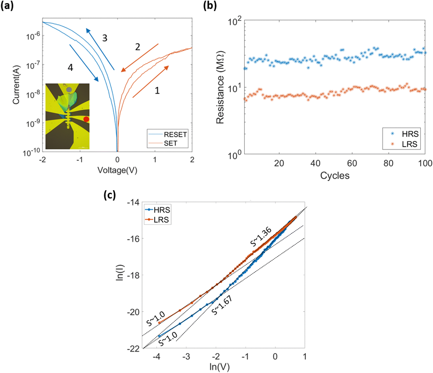 | ||
| Fig. 4 (a) Forming and compliance-free, gradual resistance switching of the device shown in the inset. From (b), consistent resistive switching endurance can be observed, with the resistance gradually increasing over cycles. (c) The lack of an abrupt filament formation prevents a runaway region from appearing in the lnln IV plot of a representative SET cycle from which we can assume transport characteristics. | ||
The device operates at low SET and RESET currents, reading 26 nA at −0.2 V (∼7.7 MΩ) in LRS compared to 7.4 nA at −0.2 V (∼27 MΩ) in HRS (Fig. 4b). The higher resistance of these devices compared to those in Fig. 2 is likely due to differences in device thickness and sample-to-sample variation. For the same oxidation parameters but higher initial HfS2 thicknesses, the remaining thickness of un-oxidised HfS2 in the device will be greater. This, in turn, reduces peak currents in the device (Fig. S6, ESI†) presenting a method for tuning the conductance and energy consumption of the device.
The stark difference in RON/ROFF in the more technologically relevant fast pulsed operation scheme (Fig. 2 – higher RON/ROFF) compared to the ramped voltage scheme used here to investigate transport in the device (Fig. 4) can be explained by the effect of Joule heating. Factors which are known to limit peak LRS conductance and hinder stability during switching such as Joule heating typically dominate over longer timescales.53 This may explain the lower RON/ROFF of the device in Fig. 4, investigated with long-timescale IV sweeps, despite the higher voltages used in this instance. We have observed very similar RON/ROFF and IV sweep characteristics even in more conductive devices. Near the SET voltage of ∼1.45 V in Fig. 4a, a small rise in conductance can be observed, but this is suppressed in IV sweep operation, likely contributed to by Joule heating and other conductance-limiting mechanisms in the device. Hence, maintaining fast switching timescales ∼80 ns in pulsed operation allows for a larger conductance modulation than with voltage ramps (Fig. 4) resulting in a higher RON/ROFF.53
In order to identify the dominating transport mechanisms, we analyse the natural logarithm of V and I for a representative SET voltage sweep, shown in Fig. 4c. The characteristics of these IV sweeps are representative of the resistance switching observed in all the devices we have fabricated with this method. The HRS and LRS portions of the SET curve are represented by blue and orange lines, respectively. In contrast to other similar devices,37 there is no abrupt and dramatic increase in conductance at the SET voltage, as described previously. This implies a conductance-mediated switching behaviour where, rather than breakdown effects such as electrode-bridging conductive filaments being formed,20 resistive switching is primarily caused by the overall field-induced redistribution of movable defects (such as oxygen vacancies) in the device.54 The electrical transport in the device seems to initially follow trap-controlled space charge limited conduction (SCLC), where there is an ohmic regime at a low voltage such that ln(I)∼ln(V), then a region where the proportionality increases to ∼1.67 emerges-closer to the relationship described by Child's law. However after this step, there is no dramatic runaway current region, yet the device still switches to an LRS. Most HfOx-based devices show Schottky emission in the high field HRS region,37,55 however this is not the case in our devices. As opposed to the more commonly used (e.g. as a gate dielectric) amorphous HfOx with low defect densities,42,56 from TEM we have observed a crystalline oxide with sulfur defects present (Fig. 1) and out-of-plane defect pathways (Fig. S2, ESI†). Other 2D material based memristive devices have shown the ability to produce low current and forming-free devices such as ours, due to pre-existing defect pathways along domain walls in (poly)crystalline oxide.45 Due to the applied field, the conductivity of this pathway could be mediated by oxygen ion or vacancy diffusion57 as described in the conductance-mediated picture.54 As the applied positive voltage from the top electrode causes the oxide region to become more sub-stoichiometric due to oxygen ion migration into the Ti electrode,58 the resistance of the oxide region can be modulated without completely breaking it down or forming a continuous metallic filament.54,57
In the LRS the electrical transport is also rather complex-showing an initial relationship of ln(I)∼1.36![[thin space (1/6-em)]](https://www.rsc.org/images/entities/char_2009.gif) ln(V) at high field, then an ohmic region at low field. This may be due to the semiconductor–oxide nature of our device, providing two additional junctions, one of which may be rectifying. These are not normally present in memristive devices, and the out-of-plane transport through the HfS2 further complicates the picture.
ln(V) at high field, then an ohmic region at low field. This may be due to the semiconductor–oxide nature of our device, providing two additional junctions, one of which may be rectifying. These are not normally present in memristive devices, and the out-of-plane transport through the HfS2 further complicates the picture.
TCAD simulation
To further understand the transport and role of the semiconductor layer in our devices, we simulated resistive switching using a technology computer aided design (TCAD) software: Sentaurus (Synopsys, 2022). We compare a vertical memristor structure with a switching layer consisting of only HfOx/HfO2 to one consisting of HfOx/HfO2/HfS2, similar to our devices.The dynamics of three particles were simulated in our modelled devices under applied field in kinetic Monte-Carlo (KMC) simulations: mobile oxygen ions (O2−), mobile oxygen vacancies (V2+O) and immobile, uncharged oxygen vacancies (VO, composing the filament). Allowing for field-driven Frenkel pair (O2− ion and V2+O oxygen vacancy) generation and recombination, we simulated resistive switching by ramping voltage in a quasistatic manner, dwelling at each voltage step for a certain period of time, recording the defect generation, particle movement in the device and the resulting conduction or leakage current (solving Poisson's equation) from the top to the bottom electrode. Spatially-dependent as opposed to spatially-agnostic vacancy generation was simulated by reducing the activation energy for Frenkel pair generation in the presence of pre-existing defects, guided by existing literature.59,60 Subsequently, filaments were generated as an energy-driven and spatially-dependent transition from free-moving, charged V2+O particles into immobile, uncharged VO particles which can carry a conduction current. Trap-assisted tunnelling processes which would make the simulation more realistic60 were omitted due to their heavy simulation time cost.
We simulated device structures as shown in Fig. 5a, using a design similar to that of existing HfOx/HfO2 memristors but with a lateral size of 8 nm × 1.5 nm to focus on the dynamics of a single filament and reduce simulation time. A Ti top electrode was modelled as an idealised contact of no thickness, on top of a 1 nm thick TiOx layer interfacing with an equally thin HfOx layer. The latter two regions were included due to the well-known gettering effect of Ti electrodes on oxides.58,61 The TiOx region therefore permitted in-and-out diffusion of O2− ions into the electrode under an applied field to simulate this effect. Frenkel pair generation in HfO2 based devices with Ti top electrodes has been shown to occur preferentially in the sub-stoichiometric HfOx region,62 so we simulate Frenkel pair generation only in the HfOx region, with the HfO2 bulk allowing V2+O diffusion and filament growth/recession under applied field. The bottom contact was a TiN idealised contact.
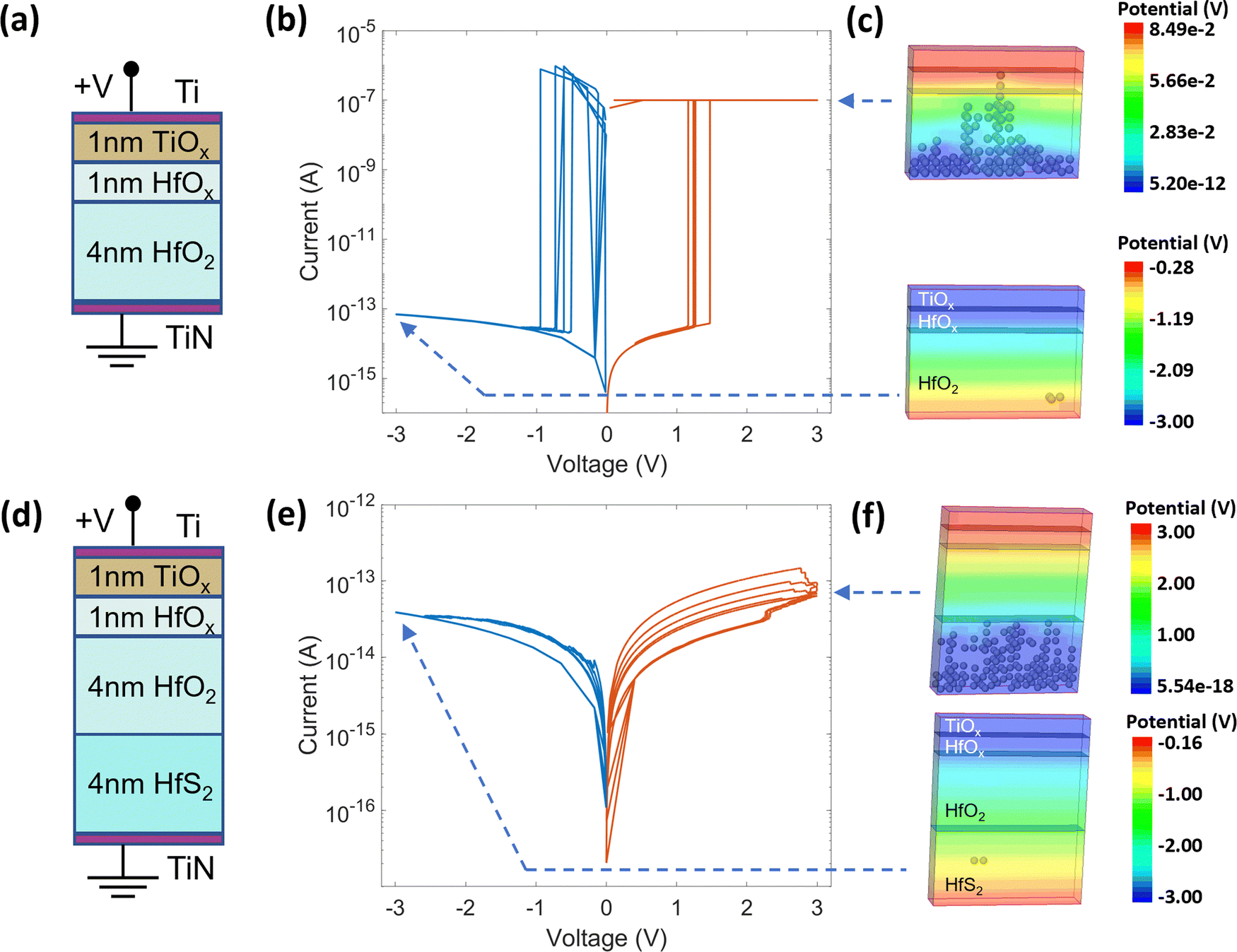 | ||
| Fig. 5 Finite-element simulation of HfO2 memristors without and with HfS2 (a) Thicknesses of each layer in the HfOx/HfO2 memristors without HfS2 (width = 1.5 nm, length = 8 nm). (b) Simulated IV sweeps of a device excluding HfS2 exhibiting abrupt switching with filament formation and dissolution shown in (c) for peak SET and RESET voltages, respectively. Electrostatic potential across the device also shows modulation of potential due to the presence of the filament in the device. Spheres in the electrostatic potential plots represent immobile vacancies (VO) comprising the filaments. (d) Structure of simulated devices including the HfS2 region. (e) Simulated IV sweeps of a device using the semiconductor–oxide structure from (d) showing gradual resistive switching, with immobile vacancy concentration (represented by spheres) shown in the HfS2 region in (f) for the peak SET and RESET voltages. A much smaller modulation of the potential due to vacancy aggregation in (f) can be seen compared to the electrode bridging filament in (c). | ||
In Fig. 5b we show representative resistive switching cycles for a Ti/TiOx/HfOx/HfO2/TiN device. The device was cycled 5 times to demonstrate the general switching characteristics while saving simulation time. The device exhibits abrupt resistive switching and requires a current compliance to prevent complete dielectric breakdown, as is common in most HfOx-based memristive devices. The particles shown in Fig. 5c are immobile vacancies (VO) comprising the conductive filament, and the voltage was applied to the top electrode. Note that for both Fig. 5c and f, oxygen ions and mobile vacancies are not visualised for ease of interpretation.
With the inclusion of a HfS2 region (Fig. 5d), we observe compliance free, gradual resistive switching (Fig. 5e) with tuneable device conductance (Fig. S6, ESI†) as in our experimental devices. The HfS2 region was simulated by starting with a template Si file and adjusting the band gap (1.23 eV) and work function (5.71 eV) parameters due to limited available material parameters for few-layer HfS2.63–66 Enabling charged vacancy diffusion and filament growth/recession mechanisms in the HfS2 region was critical for the replication of resistive switching similar to our experimental devices (Fig. S4, ESI†). A similar effect where charged oxygen vacancies migrated through HfO2 and across the HfO2/SiO2 interface has been investigated.67 The vacancy was shown to stabilise in its neutral charge state upon entering the SiO2 layer, just as we have modelled for the HfO2/HfS2 interface here. In our experimental devices, it is likely that vacancies may have migrated through out-of-plane defects present in the pristine device (Fig. S2, ESI†) which could explain the forming-free behaviour.
Notably, simply increasing the thickness of the HfO2 layer as shown in Fig. 5a to match the HfO2/HfS2 thickness shown in Fig. 5d did not lead to any significant hysteretic behaviour in the sub-switching regime and the device still showed abrupt resistive switching otherwise. Therefore, the HfS2 layer could play a vital role in limiting currents and preventing abrupt resistive switching, removing the need for current compliance. Greatly reduced peak current magnitudes can be observed in the simulated HfO2/HfS2 device compared to our fabricated devices, however this has been shown to be due to the small cross-sectional simulation area chosen (Fig. S5, ESI†). By extrapolating to the lateral area of our experimental devices, we predict similar currents in the order of nA at 1.0 V. Furthermore, we observe that the peak conductance of the device decreases with increasing HfS2 thickness (Fig. S6, ESI†), demonstrating the ability to tune the peak conductance and energy consumption of these devices based on their structure. The current observed is strongly related to the number of VO generated in the HfS2 region in the simulation (Fig. 5f). This suggests a conductance-mediated switching mechanism as the behaviour exhibited by the device is more akin to resistance switching without complete filament formation14,54,57 rather than the more abrupt and conventional filamentary bridging of the top and bottom electrodes through an amorphous hafnia switching layer. Video files showcasing the generation and diffusion of vacancies contributing to resistive switching in these devices can be accessed in the ESI† (Movies S1 and S2) with a brief description of each movie in ESI† Section S5. The simulation accuracy and current magnitudes can be improved further by the inclusion of trap-assisted tunnelling processes such as elastic and inelastic trap to band and band to trap tunnelling of electrons, treating the V2+O particles as electron traps which transition to VO particles upon electron capture.60
Conclusions
We have shown that oxide–semiconductor structures obtained by dry oxidation of HfS2 at low temperature (<300 °C) can be used to realize forming-free and compliance-free resistive memories. By using voltage pulses, we demonstrate that non-volatile resistive switching with a RON/ROFF ≈ 102 can be achieved with low energy, 80 ns pulses. We also show that the devices can exhibit resistive switching with less than 20 pJ pulses, highlighting their potential for low energy operation which is critical for ML and neuromorphic applications. Stable retention of resistance states at 150 °C has been observed, demonstrating the potential of these devices for long retention times and resilience to ageing. With the aid of IV sweeps and TCAD simulations, we investigate the transport in these devices and show that the semiconductor layer plays a key role in preventing oxide breakdown, enabling compliance-free operation and tuneable conductance/power consumption. Further work is required to determine and decouple the exact switching and transport mechanisms in the device, for example by investigating the effect of area on LRS conductance in experimental devices. However, our work has shown that both the semiconductor–oxide structure and the precise control of oxide crystallinity have a significant impact on the performance and behaviour exhibited by 2DLM-based memristors, paving the way for simplified circuits for neuromorphic computing.Methods
HfS2 production and oxidation
HfS2 flakes were prepared by mechanical exfoliation of a HfS2 crystal (HQGraphene) onto 285 nm SiO2 on Si in an inert (N2) glovebox environment. The flakes were then examined using an optical microscope and transfer system within the glovebox. Oxidation was then performed in a Moorfield Minilab 026 system integrated within the same inert environment glovebox. The flakes were heated in vacuum to a set point of 280 °C when oxidation commenced for 110 minutes at 0.1 mbar in a dry O2 environment with a flow rate of 38 SCCM. The samples were then allowed to cool in vacuum.Ellipsometry measurements
Ellipsometry measurements are performed using an EP4 Spectroscopic Imaging Ellipsometer (SIE, Park Systems Gmbh, Göttingen), equipped with a laser-stabilized Xenon arc lamp and a three-grating monochromator as a spectroscopic light source. This allows for an available spectral range between 360 nm to 1000 nm, and a ∼5 nm bandwidth of the output line. A polarization state generator (PSG), comprised of a linear polarizer and a quarter-wave plate (compensator), controls the state of polarization of the incident beam. The reflected light is collected through an analyzer and a 50× objective to a 1392 × 1040 pixel CCD camera, allowing for a lateral resolution down to 1 μm. All measurements are performed in the P-A-nulling mode, at an incidence angle of 50° with respect to the surface normal.TEM lamellar fabrication and characterisation
The cross-sectional lamellae were prepared using a DualBeam FIB-SEM system (Carl Zeiss Auriga), equipped with a platinum (Pt) deposition cartridge and a nanomanipulator (Kleindiek Nanotechnik). To minimize the ion beam damage, the sample was first protected by a ∼100 nm platinum layer by electron beam deposition (2 kV). After that, several micrometer-thick platinum layers were deposited using a gallium ion beam. After rough milling by 30 kV ion beam, a ∼2 μm thick plate was lifted out and attached to the edge of a copper finger, following thinning processes using a 15 kV ion beam to minimize the ion beam damage and the final lamella was less than 100 nm thick. After thinning, the lamella was transferred to the TEM column for observation as soon as possible to minimise potential further oxidation. Transmission electron microscopy (TEM) and scanning TEM (STEM) were performed using uncorrected FEI Titan 80–300 with a Schottky field emission S-FEG source operated at 300 kV. Electron energy-loss spectroscopy (EELS) maps were carried out with a Gatan Quantum spectrometer with an energy dispersion of 0.5 eV per channel.Device fabrication
Bottom electrodes were fabricated by a direct-write lithography method, evaporating 5 nm of chrome as an adhesion layer, and then 65 nm of gold by electron beam evaporation. Lift-off was performed in Dimethyl sulfoxide (DMSO) at 65 °C for 10 minutes. Flakes of HfS2 used in devices were transferred by a polycarbonate (PC) stamp, which was melted onto the bottom electrodes at 180 °C. The residual PC was dissolved in chloroform and the device was cleaned with acetone and IPA cleaning. Subsequently, the flakes were partially oxidized following the protocol described above. Finally, direct-write lithography was used to pattern the top electrode and 5 nm of titanium then 65 nm of gold was deposited by electron beam (e-beam) evaporation, with the lift-off performed the same as before.Device characterisation
Devices were measured on a FormFactor (formerly Cascade) MPS150 probe station, connected to a Keysight B1500A Parameter Analyzer with remote sensing units and a waveform generator/fast measurement unit (WGFMU) with a temporal resolution of 10 ns. Oscilloscope measurements were performed with a 1 GHz Keysight P9243A oscilloscope. Measurements above room temperature and in vacuum were conducted with a 6-probe Nextron MPS-PTH chamber equipped with a Peltier stage and connected to a dry pump.Sentaurus TCAD simulations
Simulations were performed in Synopsys Sentaurus TCAD. Device structures were designed in SDE, with a mesh size of 0.5 nm and no doping. A template Silicon parameter file was used to represent HfS2 in the device structure. Ti and TiN electrodes were simulated as idealised contacts. In SDevice, Kinetic Monte Carlo (KMC) simulations were used to show the time evolution of oxygen vacancies and oxygen ion generation, diffusion, and filament growth/recession dynamics dependent on applied voltage to the simulated structures. SVisual TCL command files were used to produce particle plots, IV characteristics and animations included in ESI.†Data availability
Data for this article, including scripts used to plot figures in the main text and ESI† are available in the UCL research data repository, at https://doi.org/10.5522/04/27186993.v1.Conflicts of interest
The authors declare that they have no competing interests.Acknowledgements
We acknowledge helpful discussions with Abin Varghese and Bipin Rajendran. AXh and AL acknowledge funding from EPSRC, EP/T517793/1. AA acknowledges funding from The Ministry of Education of Saudi Arabia. VN and XG wish to thank the support of the Science Foundation Ireland funded AMBER research centre (Grant No. 12/RC/2278P2), and the Frontiers for the Future award (Grant No. 20/FFP-A/8950). Furthermore, VN and XG wish to thank the Advanced Microscopy Laboratory in CRANN for the provision of their facilities. SH and IC acknowledge funding from EPSRC (EP/T001038/1,EP/V047515/1, EP/N509620/1, EP/R513180/1).References
- A. Mehonic and A. J. Kenyon, Brain-inspired computing needs a master plan, Nature, 2022, 604(7905), 255–260 CrossRef CAS.
- N. Jones, et al., How to stop data centres from gobbling up the world's electricity, Nature, 2018, 561(7722), 163–166 CrossRef CAS.
- D. Silver, A. Huang, C. J. Maddison, A. Guez, L. Sifre, G. V. D. Driessche, J. Schrittwieser, I. Antonoglou, V. Panneershelvam and M. Lanctot, et al., Mastering the game of go with deep neural networks and tree search, Nature, 2016, 529(7587), 484–489 CrossRef CAS.
- X. Guo and Y. Su, Neuromorphic photonics: development of the field, Neuromorphic Photonic Devices and Applications, Elsevier, 2024, pp. 69–110 Search PubMed.
- A. Oleinik, What are neural networks not good at? On artificial creativity, Big Data Soc., 2019, 6(1), 2053951719839433 CrossRef.
- D. Marković, A. Mizrahi, D. Querlioz and J. Grollier, Physics for neuromorphic computing, Nat. Rev. Phys., 2020, 2(9), 499–510 CrossRef.
- G. W. Burr, R. M. Shelby, A. Sebastian, S. Kim, S. Kim, S. Sidler, K. Virwani, M. Ishii, P. Narayanan and A. Fumarola, et al., Neuromorphic computing using non-volatile memory, Adv. Phys.:X, 2017, 2(1), 89–124 Search PubMed.
- A. Mehonic, A. Sebastian, B. Rajendran, O. Simeone, E. Vasilaki and A. J. Kenyon, Memristors–from in-memory computing, deep learning acceleration, and spiking neural networks to the future of neuromorphic and bio-inspired computing, Adv. Intell. Syst., 2020, 2(11), 2000085 CrossRef.
- L. Chua, Memristor-the missing circuit element, IEEE Trans. Circuit Theory, 1971, 18(5), 507–519 Search PubMed.
- F. Argall, Switching phenomena in titanium oxide thin films, Solid-State Electron., 1968, 11(5), 535–541 CrossRef.
- D. B. Strukov, G. S. Snider, D. R. Stewart and R. Stanley Williams, The missing memristor found, Nature, 2008, 453(7191), 80–83 CrossRef PubMed.
- A. Mehonic, S. Cueff, M. Wojdak, S. Hudziak, O. Jambois, C. Labbé, B. Garrido, R. Rizk and A. J. Kenyon, Resistive switching in silicon suboxide films, J. Appl. Phys., 2012, 111(7), 074507 CrossRef.
- Y. Zhang, G.-Q. Mao, X. Zhao, Y. Li, M. Zhang, Z. Wu, W. Wu, H. Sun, Y. Guo and L. Wang, et al., Evolution of the conductive filament system in HfO2-based memristors observed by direct atomic-scale imaging, Nat. Commun., 2021, 12(1), 7232 CrossRef PubMed.
- Z.-X. Tang, W.-W. Tang, X.-G. Tang, Q.-X. Liu, Y.-P. Jiang, W.-H. Li, Z.-H. Tang, X.-B. Guo and Z.-F. Tang, Analog-type resistive switching behavior of Au/HfO2/ZnO memristor fabricated on flexible mica substrate, Phys. E, 2020, 120, 114047 CrossRef.
- M. Li, H. Liu, R. Zhao, F.-S. Yang, M. Chen, Y. Zhuo, C. Zhou, H. Wang, Y.-F. Lin and J. Joshua Yang, Imperfection-enabled memristive switching in van der Waals materials, Nat. Electron., 2023, 6(7), 491–505 CrossRef.
- M. Wang, S. Cai, C. Pan, C. Wang, X. Lian, Y. Zhuo, K. Xu, T. Cao, X. Pan and B. Wang, et al., Robust memristors based on layered two-dimensional materials, Nat. Electron., 2018, 1(2), 130–136 Search PubMed.
- X. Wu, R. Ge, D. Akinwande and J. C. Lee, Memristors based on 2D monolayer materials, in Memristor-An Emerging Device for Post-Moore's Computing and Applications, IntechOpen, 2021 Search PubMed.
- J. Yang, A. Yoon, D. Lee, S. Song, I. John Jung, D.-H. Lim, H. Jeong, Z. Lee, M. Lanza and S.-Y. Kwon, Wafer-scale memristor array based on aligned grain boundaries of 2D molybdenum ditelluride for application to artificial synapses, Adv. Funct. Mater., 2024, 34(15), 2309455 CrossRef.
- K. Zhu, S. Pazos, F. Aguirre, Y. Shen, Y. Yuan, W. Zheng, O. Alharbi, M. A. Villena, B. Fang and X. Li, et al., Hybrid 2D-CMOS microchips for memristive applications, Nature, 2023, 618(7963), 57–62 CrossRef CAS PubMed.
- U. Celano, A. Fantini, R. Degraeve, M. Jurczak, L. Goux and W. Vandervorst, Scalability of valence change memory: From devices to tip-induced filaments, AIP Adv., 2016, 6(8), 085009 CrossRef.
- J. A. Kittl, K. Opsomer, M. Popovici, N. Menou, B. Kaczer, X. Peng Wang, C. Adelmann, M. A. Pawlak, K. Tomida and A. Rothschild, et al., High-k dielectrics for future generation memory devices, Microelectron. Eng., 2009, 86(7–9), 1789–1795 CrossRef CAS.
- C. Li, M. Hu, Y. Li, H. Jiang, N. Ge, E. Montgomery, J. Zhang, W. Song, N. Dávila and C. E. Graves, et al., Analogue signal and image processing with large memristor crossbars, Nat. Electron., 2018, 1(1), 52–59 CrossRef.
- B. Govoreanu, G. S. Kar, Y. Y. Chen, V. Paraschiv, S. Kubicek, A. Fantini, I. P. Radu, L. Goux, S. Clima and R. Degraeve, et al., 10 × 10 nm2 Hf/HfOx crossbar resistive RAM with excellent performance, reliability and low-energy operation, IEEE Int. Electron Devices Meet., 2011, 31–36 Search PubMed.
- Z. Peng, F. Wu, L. Jiang, G. Cao, B. Jiang, G. Cheng, S. Ke, K.-C. Chang, L. Li and C. Ye, HfO2-based memristor as an artificial synapse for neuromorphic computing with tri-layer HfO2/BiFeO3/HfO2 design, Adv. Funct. Mater., 2021, 31(48), 2107131 CrossRef CAS.
- E. Covi, S. Brivio, A. Serb, T. Prodromakis, M. Fanciulli and S. Spiga, Hfo2-based memristors for neuromorphic applications, In 2016 IEEE International Symposium on Circuits and Systems (ISCAS), pp. 393–396, IEEE, 2016.
- J. Liu, H. Yang, Z. Ma, K. Chen, X. Huang and K. Wang, HfO2/TiOx bilayer structure memristor with linear conductance tuning for high density memory and neuromorphic computing, J. Appl. Phys., 2020, 128(18), 184902 CrossRef CAS.
- K. S. Novoselov, A. K. Geim, S. V. Morozov, D.-E. Jiang, Y. Zhang, S. V. Dubonos, I. V. Grigorieva and A. A. Firsov, Electric field effect in atomically thin carbon films, Science, 2004, 306(5696), 666–669 CrossRef CAS PubMed.
- S. Haastrup, M. Strange, M. Pandey, T. Deilmann, P. S. Schmidt, N. F. Hinsche, M. N. Gjerding, D. Torelli, P. M. Larsen and A. C. Riis-Jensen, et al., The computational 2D materials database: high-throughput modeling and discovery of atomically thin crystals, 2D Mater., 2018, 5(4), 042002 CrossRef CAS.
- H. Duan, S. Cheng, L. Qin, X. Zhang, B. Xie, Y. Zhang and W. Jie, Low-power memristor based on two-dimensional materials, J. Phys. Chem. Lett., 2022, 13(31), 7130–7138 CrossRef CAS.
- L. Prozorovska and P. R. Kidambi, State-of-the-art and future prospects for atomically thin membranes from 2D materials, Adv. Mater., 2018, 30(52), 1801179 CrossRef.
- C. Liu, H. Chen, S. Wang, Q. Liu, Y.-G. Jiang, D. W. Zhang, M. Liu and P. Zhou, Two-dimensional materials for next-generation computing technologies, Nat. Nanotechnol., 2020, 15(7), 545–557 CrossRef CAS.
- A. K. Geim and I. V. Grigorieva, van der Waals heterostructures, Nature, 2013, 499(7459), 419–425 CrossRef CAS PubMed.
- D. G. Purdie, N. M. Pugno, T. Taniguchi, K. Watanabe, A. C. Ferrari and A. Lombardo, Cleaning interfaces in layered materials heterostructures, Nat. Commun., 2018, 9(1), 5387 CrossRef.
- S. Chen, M. R. Mahmoodi, Y. Shi, C. Mahata, B. Yuan, X. Liang, C. Wen, F. Hui, D. Akinwande and D. B. Strukov, et al., Wafer-scale integration of two-dimensional materials in high-density memristive crossbar arrays for artificial neural networks, Nat. Electron., 2020, 3(10), 638–645 CrossRef.
- Y. Yuan, J. Weber, J. Li, B. Tian, Y. Ma, X. Zhang, T. Taniguchi, K. Watanabe and M. Lanza, On the quality of commercial chemical vapour deposited hexagonal boron nitride, Nat. Commun., 2024, 15(1), 4518 CrossRef PubMed.
- A. AlMutairi, A. Xhameni, X. Guo, I. Chircă, V. Nicolosi, S. Hofmann and A. Lombardo, Controlled fabrication of native ultra-thin amorphous gallium oxide from 2D gallium sulfide for emerging electronic applications, Adv. Mater. Interfaces, 2024, 2400481 Search PubMed.
- L. Liu, Y. Li, X. Huang, J. Chen, Z. Yang, K.-H. Xue, M. Xu, H. Chen, P. Zhou and X. Miao, Low-power memristive logic device enabled by controllable oxidation of 2d HfSe2 for in-memory computing, Adv. Sci., 2021, 8(15), 2005038 CrossRef.
- T. Jin, Y. Zheng, J. Gao, Y. Wang, E. Li, H. Chen, X. Pan, M. Lin and W. Chen, Controlling native oxidation of HfS2 for 2D materials based flash memory and artificial synapse, ACS Appl. Mater. Interfaces, 2021, 13(8), 10639–10649 CrossRef.
- Y. Y. Wang, S. M. Huang, K. Yu, J. Jiang, Y. Liang, B. Zhong, H. Zhang, G. F. Kan, S. F. Quan and J. Yu, Atomically flat HfO2 layer fabricated by mild oxidation HfS2 with controlled number of layers, J. Appl. Phys., 2020, 127(21), 214303 CrossRef.
- N. Peimyoo, M. D. Barnes, J. D. Mehew, A. De Sanctis, I. Amit, J. Escolar, K. Anastasiou, A. P. Rooney, S. J. Haigh and S. Russo, et al., Laser-writable high-k dielectric for van der Waals nanoelectronics, Sci. Adv., 2019, 5(1), eaau0906 CrossRef PubMed.
- S. Ng, R. A. John, J.-T. Yang and N. Mathews, Forming-less compliance-free multistate memristors as synaptic connections for brain-inspired computing, ACS Appl. Electron. Mater., 2020, 2(3), 817–826 CrossRef.
- Y. Sun, X. Yan, X. Zheng, Y. Liu, Y. Zhao, Y. Shen, Q. Liao and Y. Zhang, High on-off ratio improvement of ZnO-based forming-free memristor by surface hydrogen annealing, ACS Appl. Mater. Interfaces, 2015, 7(13), 7382–7388 CrossRef.
- B. Yang, N. Xu, C. Li, C. Huang, D. Ma, J. Liu, D. Arum and L. Fang, A forming-free ReRAM cell with low operating voltage, IEICE Electron. Express, 2020, 17(22), 20200343 CrossRef.
- F. F. Athena, M. P. West, J. Hah, S. Graham and E. M. Vogel, Trade-off between gradual set and on/off ratio in HfOx-based analog memory with a thin SiOx barrier layer, ACS Appl. Electron. Mater., 2023, 5(6), 3048–3058 CrossRef PubMed.
- X. Feng, S. Li, S. L. Wong, S. Tong, L. Chen, P. Zhang, L. Wang, X. Fong, D. Chi and K.-W. Ang, Self-selective multi-terminal memtransistor crossbar array for in-memory computing, ACS Nano, 2021, 15(1), 1764–1774 CrossRef PubMed.
- P.-Y. Chen, B. Lin, I.-T. Wang, T.-H. Hou, J. Ye, S. Vrudhula, J.-S. Seo, Y. Cao and S. Yu, Mitigating effects of non-ideal synaptic device characteristics for on-chip learning, In 2015 IEEE/ACM International Conference on Computer-Aided Design (ICCAD), pp. 194–199, IEEE, 2015.
- V. T. Renard, M. Jublot, P. Gergaud, P. Cherns, D. Rouchon, A. Chabli and V. Jousseaume, Catalyst preparation for cmos-compatible silicon nanowire synthesis, Nat. Nanotechnol., 2009, 4(10), 654–657 CrossRef PubMed.
- X. Xiong, J. Kang, Q. Hu, C. Gu, T. Gao, X. Li and Y. Wu, Reconfigurable logic-in-memory and multilingual artificial synapses based on 2D heterostructures, Adv. Funct. Mater., 2020, 30(11), 1909645 CrossRef.
- W. Huh, S. Jang, J. Y. Lee, D. Lee, D. Lee, J. M. Lee, H.-G. Park, J. C. Kim, H. Y. Jeong and G. Wang, et al., Synaptic barristor based on phase-engineered 2D heterostructures, Adv. Mater., 2018, 30(35), 1801447 CrossRef PubMed.
- H. Tian, Q. Guo, Y. Xie, H. Zhao, C. Li, J. J. Cha, F. Xia and H. Wang, Anisotropic black phosphorus synaptic device for neuromorphic applications, Adv. Mater., 2016, 28, 4991–4997 CrossRef PubMed.
- H.-K. He, R. Yang, H.-M. Huang, F.-F. Yang, Y.-Z. Wu, J. Shaibo and X. Guo, Multi-gate memristive synapses realized with the lateral heterostructure of 2D WSe2 and WO3, Nanoscale, 2020, 12(1), 380–387 RSC.
- B. Rajendran, Building a smart and green AI, Electrochem. Soc. Interface, 2023, 32(1), 47 CrossRef.
- S. S. Teja Nibhanupudi, A. Roy, D. Veksler, M. Coupin, K. C. Matthews, M. Disiena, A. Ansh, J. V. Singh, I. R. Gearba-Dolocan, J. Warner, J. P. Kulkarni, G. Bersuker and S. K. Banerjee, et al., Ultra-fast switching memristors based on two-dimensional materials, Nat. Commun., 2024, 15(1), 2334 CrossRef.
- D. Li, B. Wu, X. Zhu, J. Wang, B. Ryu, W. D. Lu, W. Lu and X. Liang, MoS2 memristors exhibiting variable switching characteristics toward biorealistic synaptic emulation, ACS Nano, 2018, 12(9), 9240–9252 CrossRef.
- M. Ismail, Z. Batool, K. Mahmood, A. M. Rana, B.-D. Yang and S. Kim, Resistive switching characteristics and mechanism of bilayer HfO2/ZrO2 structure deposited by radio-frequency sputtering for nonvolatile memory, Results Phys., 2020, 18, 103275 CrossRef.
- J. J. Yang, I. H. Inoue, T. Mikolajick and C. S. Hwang, Metal oxide memories based on thermochemical and valence change mechanisms, MRS Bull., 2012, 37(2), 131–137 CrossRef.
- L.-H. Li, K.-H. Xue, J.-H. Yuan, G.-Q. Mao and X. Miao, Hafnia for analog memristor: Influence of stoichiometry and crystalline structure, Phys. Rev. Mater., 2022, 6(8), 084603 CrossRef.
- I. Valov, M. Luebben, A. Wedig and R. Waser, Mobile ions, transport and redox processes in memristive devices, ECS Trans., 2016, 75(5), 27 CrossRef CAS.
- S. R. Bradley, A. L. Shluger and G. Bersuker, Electron-injection-assisted generation of oxygen vacancies in monoclinic HfO2, Phys. Rev. Appl., 2015, 4(6), 064008 CrossRef.
- A. Zeumault, S. Alam, Z. Wood, R. J. Weiss, A. Aziz and G. S. Rose, TCAD modeling of resistive-switching of HfO2 memristors: Efficient device-circuit co-design for neuromorphic systems, Front. Nanotechnol., 2021, 3, 734121 CrossRef.
- V. L. Stout and M. D. Gibbons, Gettering of gas by titanium, J. Appl. Phys., 1955, 26(12), 1488–1492 Search PubMed.
- X. Xu, B. Rajendran and M. P. Anantram, Kinetic monte carlo simulation of interface-controlled hafnia-based resistive memory, IEEE Trans. Electron Devices, 2019, 67(1), 118–124 Search PubMed.
- T. Kanazawa, T. Amemiya, A. Ishikawa, V. Upadhyaya, K. Tsuruta, T. Tanaka and Y. Miyamoto, Few-layer HfS2 transistors, Sci. Rep., 2016, 6(1), 22277 CrossRef.
- C. Gong, H. Zhang, W. Wang, L. Colombo, R. M. Wallace and K. Cho, Band alignment of two-dimensional transition metal dichalcogenides: Application in tunnel field effect transistors, Appl. Phys. Lett., 2013, 103(5), 053513 CrossRef.
- S. Netsu, T. Kanazawa, T. Uwanno, T. Amemiya, K. Nagashio and Y. Miyamoto, Type-II HfS2/MoS2 heterojunction transistors, IEICE Trans. Electron., 2018, 101(5), 338–342 CrossRef.
- C. Zhang, C. Gong, Y. Nie, K.-A. Min, C. Liang, Y. J. Oh, H. Zhang, W. Wang, S. Hong and L. Colombo, et al., Systematic study of electronic structure and band alignment of monolayer transition metal dichalcogenides in van der Waals heterostructures, 2D Mater., 2016, 4(1), 015026 CrossRef.
- N. Capron, P. Broqvist and A. Pasquarello, Migration of oxygen vacancy in HfO2 and across the HfO2/SiO2 interface: A first-principles investigation, Appl. Phys. Lett., 2007, 91(19), 192905 CrossRef.
Footnote |
| † Electronic supplementary information (ESI) available. See DOI: https://doi.org/10.1039/d4nh00508b |
| This journal is © The Royal Society of Chemistry 2025 |