
 Open Access Article
 This Open Access Article is licensed under a Creative Commons Attribution-Non Commercial 3.0 Unported Licence
Synthesis, redox exfoliation, and magnetic nanoparticle decoration of VSe2 and SnSe2 nanosheets†
Zhengxi
Xuan
ab,
Zheng
Fu
ab,
B. Medini
Rajapakse
 c,
Ali
Jawaid
d,
Shuo
Liu
af,
Richard A.
Vaia
*d,
Luis
Velarde
*c,
Paras N.
Prasad
*ce and
Mark T.
Swihart
*abe
c,
Ali
Jawaid
d,
Shuo
Liu
af,
Richard A.
Vaia
*d,
Luis
Velarde
*c,
Paras N.
Prasad
*ce and
Mark T.
Swihart
*abe
aDepartment of Chemical and Biological Engineering, University at Buffalo, The State University of New York, Buffalo 14260, NY, USA. E-mail: swihart@buffalo.edu
bRENEW Institute, University at Buffalo, The State University of New York, Buffalo 14260, NY, USA
cDepartment of Chemistry, University at Buffalo, The State University of New York, Buffalo 14260, NY, USA. E-mail: lvelarde@buffalo.edu; pnprasad@buffalo.edu
dMaterials and Manufacturing Directorate, Air Force Research Laboratories, WPAFB, Ohio 45433, USA
eInstitute for Lasers, Photonics, and Biophotonics, The State University of New York, Buffalo 14260, NY, USA
fThe Molecular Foundry, Lawrence Berkeley National Lab, Berkeley, CA 94720, USA
First published on 16th June 2025
Abstract
Nanostructures exfoliated from layered van der Waals materials have attracted attention based upon their thickness-dependent optical and electronic properties. While magnetism has been observed in such 2D materials, available approaches to modulate or enhance their magnetic response remain limited. Thus, the magnetic response of 2D materials is of particular interest. Relatively few reports focus on colloidal routes to synthesize layered materials from which 2D nanostructures can be obtained by exfoliation. Herein, we present a general method to synthesize bulk vanadium diselenide (VSe2) and dual-phase tin diselenide SnSe2–SnSe followed by liquid phase redox exfoliation to delaminate these materials into 2D nanostructures of different thicknesses. The delamination process induces phase changes, affecting the overall magnetic and optical behavior. The magnetization of these 2D nanostructures of different thicknesses increases with an increasing exfoliation degree (decreasing size and thickness). Moreover, we decorated these 2D nanostructures with colloidally synthesized iron oxide dots (FexOy, ∼4 nm diameter). This enhanced the magnetic response, which reached a saturation magnetization of 32 emu g−1 for VSe2–FexOy and 2.7 emu g−1 for SnSe2–FexOy. A synergistic effect is observed, in which the magnetization of the FexOy decorated VSe2 significantly exceeds that of either FexOy itself or VSe2 alone. This report provides a general method to synthesize 2D nanostructures of varied thickness and to decorate them with magnetic nanoparticles to achieve synergistic magnetic response.
Introduction
Two-dimensional materials, including transition-metal dichalcogenides (TMDs), graphene, and related structures, feature weak van der Waals (vdW) interactions between their atomically thin layers and strong covalent bonds within the layers. This allows them to be exfoliated into single- or few-layer films with properties that depend upon the number of atomic layers. In recent studies, several synthesis methods have been applied for the preparation of 2D magnetic materials, including the ion exchange method,1 chemical vapor deposition (CVD)2 and molecular beam epitaxy.3 Various 2D materials exhibit strong nonlinear optical properties4–6 and semiconducting7,8 properties that make them promising materials for optical sensing9,10 and energy harvesting.11–13 Other promising applications for TMDs harness their large surface area and tunable bandgap for oxygen evolution electrocatalysis14,15 and photodetection.6,16,17 Some other current research studies explore 2D magnets, including bilayer CrI3 with a reported Curie temperature (Tc) of 61.5 K18 and mechanically exfoliated Cr2Ge2Te6 with Tc of 66 K.19Most 2D materials have no magnetic ordering due to the absence of magnetic elements or unsaturated bonds.20 Likewise, modulation of magnetic behavior is difficult in most 2D layered structures. Pristine VSe2 may exhibit “frustrated intrinsic magnetism”,3 from which ferromagnetic behavior may be introduced by doping21 or by defects generated during the exfoliation process.22 Dopants and defects can alter the electronic structure, causing strong interactions between spin impurities. Thus, doping a transition metal into a 2D layered structure can be an effective way to introduce magnetic ordering.23–26 Substitution of metal atoms within the 2D structure network (MX2, where M is the metal atom and X is the chalcogen atom) has been shown to induce ferromagnetic response and enhance coercivity in 2D materials.25,27,28 For example, an Fe-doped SnSe layered structure exhibited a large coercivity of ∼1960 Oe and a Curie temperature (Tc) above room temperature.26 Non-magnetic doped 2D layered structures have also achieved modulation of coercivity; doping Bi into SnSe2 induced a large coercivity of 4400 Oe.29
Here, we report a general colloidal liquid phase method for synthesizing 1T-VSe2 and 2H-SnSe2 materials, exfoliating these materials, and decorating them with FexOy nanoparticles to modulate their magnetic response. The 2D bulk materials were synthesized in solution at relatively high temperature (∼320 °C) and then processed into thinner layered nanostructures through a redox exfoliation method. In this approach, oxidation of Layered Transition Metal Dichalcogenides (LTMDs), such as MoS2, generates metal oxide precursors (MOPs) that are adsorbed onto the bulk transition metal dichalcogenide as they are reduced. Highly charged polyoxometalates (POMs) condense onto the bulk material surface and create coulombic repulsion forces that promote material delamination during ultrasonication. Centrifugation at different speeds is then used to size-select less-exfoliated (collected at lower speed and lower RCF) and more-exfoliated (collected at higher speed and higher RCF) fractions. The centrifugal force required to collect a 2D material is a strong function of its surface-to-volume ratio, which increases steeply with the decreasing number of layers. This report demonstrates ultrasonication assisted production of liquid phase exfoliated VSe2 and SnSe2–SnSe nanosheets. This exfoliation method that delaminated VSe2 also yielded pure selenium along with VSe2. In this case, size separation by centrifugation showed that the smallest material (highest RCF) was predominantly pure selenium. Exfoliation of dual phase SnSe2–SnSe yielded mainly SnSe2, but some SnSe phase remained present. The overall crystallinity decreased with increasing RCF (smaller size) but evidence of SnSe persisted. Furthermore, we coupled these 2D layered structures with FexOy to induce magnetization in the hybrid material. The resulting material exhibited substantial saturation magnetization and coercivity. This work thus demonstrates a general colloidal method to synthesize and exfoliate 2D nanosheets and to integrate the resulting 2D layered structure with FexOy nanoparticles.
Results and discussion
Scheme 1 and Fig. 1 present the overall process for synthesis and exfoliation of bulk 2D materials reported here. Scheme 1 shows that the transition metal precursor and selenium first dissolve in a high-boiling-point solvent, followed by nucleation and growth of particles at high temperature, forming layered structures. These bulk materials were produced in the stable 2H-SnSe2 and metastable 1T-VSe2 layered phases, respectively.30 These materials were the starting point for the exfoliation process illustrated in Fig. 1. Panels (a) and (b) illustrate exfoliation from bulk materials to layered structures of different thicknesses. Panel (c) illustrates decoration of the exfoliated layered structures with FexOy. In the liquid phase redox exfoliation method (see the Experimental section), the MOPs are reduced to polyoxometalate clusters (POMs) that intercalate between layers and generate repulsive coulombic interactions that drive the material to delaminate into nanostructures of varying thickness. Using different centrifugation speeds allows collection of fractions of more- and less exfoliated material. The remaining ligand on the layer surface assists in FexOy decoration. In the following discussion, we defined RCF 150 (material collected at a relative centrifugal force of 150) as the thickest layered structure. Likewise, RCF 300 refers to the fraction collected by centrifuging at 300 RCF for 2 hours and so on for RCF 500 and RCF 1000, respectively. | ||
| Scheme 1 Solution-phase synthesis of 2D layered nanosheets. (a) VO(acac)2 or (b) Sn(acac)2, along with Se, was dissolved separately in oleylamine, where each reacted individually (in separate experiments) to form (c) bulk nanostructured materials, resulting in (d) 2H-SnSe2 or (e) 1T-VSe2 nanostructures, respectively. | ||
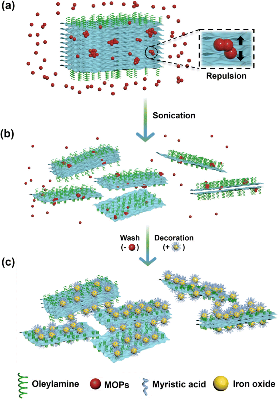 | ||
| Fig. 1 Mechanism of redox exfoliation of TMDs and their decoration with FexOy. (a) MOPs (red) assemble into polyoxometalates and adsorb on the bulk material during reduction. (b) Bulk materials are exfoliated to layered nanostructures of varying thickness. (c) FexOy (yellow) with myristic acid (blue) on their surfaces are coupled with exfoliated nanosheets. | ||
Structural characterization of 2D layered structures
In Fig. 2, panels (a1) (pre-exfoliated VSe2) to (a5) (VSe2 RCF 1000–Se) and panels (d1) (pre-exfoliated SnSe2) to (d5) (SnSe2 RCF 1000) show representative TEM images illustrating the size change from pre-exfoliated bulk materials to the thinnest nanostructures. Specifically, we added “–Se” as a suffix to identify VSe2 samples that were converted to single-phase selenium during exfoliation. Overall, increasing exfoliation results in a thickness decrease evident from the contrast difference in the TEM images; the lighter contrast regions correspond to thinner layered structures. The 2D layer thickness was further confirmed by atomic force microscopy (AFM), as shown in Fig. S1 and S2† Non-exfoliated VSe2 has a relatively large thickness of ∼150 nm that decreased to ∼20 nm with an increasing degree of exfoliation. Due to the potential aggregation of the layered structures during the sample preparation and drying process as seen in TEM images, we acquired the height profiles for the thinnest portions of each sample. Fig. 2(b) and (e) provide the XRD patterns for MX2 with different exfoliation levels. Among the VSe2 samples, a change in the phase occurs during the exfoliation process; pre-exfoliated VSe2 and VSe2 RCF 150 exhibit clear peaks corresponding to the 1T-VSe2 crystal structure. With an increasing degree of exfoliation, however, the VSe2 RCF 300–Se XRD pattern is dominated by peaks corresponding to elemental Se, and the VSe2 peaks are nearly gone. VSe2 RCF 500–Se and VSe2 RCF 1000–Se exhibit only elemental Se peaks. This suggests that the redox exfoliation process induces partial degradation of the initial 1T-phase VSe2. We also note that the 1T-phase VSe2 is thermodynamically metastable,31 which may be a factor in its degradation. As shown in Fig. 2(c) and S3,† the Raman spectra also indicated a structural transition between VSe2 RCF 150 to VSe2 RCF 300–Se consistent with the XRD results. For the thicker samples of layered metal dichalcogenides, the Raman spectrum showed an in-plane E2g peak at 145 cm−1 and out-of-plane A1g peak at 230 cm−1 confirming the fingerprint of 1T-VSe2 in non-exfoliated and RCF 150 samples.22,32 The broad but low intensity peak for all the samples at wavenumbers from 940 cm−1 to 990 cm−1 may be due to fluorescence. The dominant narrow peak at 520 cm−1 observed in all Raman spectra represents the silicon substrate that was also used in AFM measurements. | ||
| Fig. 2 Characterization of VSe2 and SnSe2 nanosheets. (a) Panels (a1)–(a5) show representative TEM images for different levels of exfoliation of VSe2; (b) XRD patterns and (c) Raman spectra for the VSe2 samples as labeled. (d) Panels (d1)–(d5) provide representative TEM images for different levels of exfoliation of SnSe2; (e) XRD patterns and (f) Raman spectra for SnSe2 samples as labeled. | ||
Similarly, in Fig. 2(e), the XRD pattern also shows a crystallinity change between the dual phase SnSe2–SnSe bulk material to predominantly SnSe2 with a smaller amount of residual SnSe. Panel (d1) shows a TEM image of bulk SnSe2–SnSe with darker contrast and overlapping multiple layered structures. The continuous exfoliation resulted in thinner layered structures (panel (d2)) until single nano-flakes were evident (panel (d5)). These results were also confirmed by AFM (Fig. S2†), from bulk-like SnSe2 with ∼600 nm thickness to single nanoflakes with a thickness of ∼10 nm. The XRD patterns in Fig. 2(e) show that the pre-exfoliation sample and SnSe2 RCF 150 exhibit peaks corresponding to both SnSe2 and SnSe. The secondary crystal phase, SnSe, is less evident with an increased level of exfoliation, leaving mainly SnSe2 present at RCF 500 (panel (d4)) and RCF 1000 (panel (d5)). In the Raman spectra shown in Fig. 2(f) and S4,† the peaks located at 100 cm−1 and 180 cm−1 are fingerprints of SnSe2, representing in-plane Eg and out-of-plane vibrational A1g mode, respectively, consistent with previous studies.33 The Raman signal with sub-peaks at 71 cm−1 and 151 cm−1 reveals the presence of SnSe.34 At the same time, two minor or weak Raman peaks were present at 1400 cm−1 and 1600 cm−1. These peaks are attributed to the ligands on the nanostructures' surfaces.35 However, the Raman intensity of the organic groups is negligible compared to that of the metallic peak (Fig. S4c†).
We took advantage of the resulting hydrophobic surface with dilute ligand coverage to attach iron oxide dots (FexOy) to these materials, inducing a magnetic response. Fig. 3 provides TEM images of FexOy-decorated VSe2 and SnSe2–SnSe nanostructures obtained by simple heating of mixed VSe2 or SnSe2–SnSe with pre-synthesized ligand-coated FexOy, resulting in ferromagnetic behavior (Fig. 4). Fig. S5† provides HRTEM images that represent FexOy distributed on the layer surfaces. The size of FexOy was approximately 4 nm in diameter (Fig. S6a†). Because of their small size, they cannot be definitively identified as Fe3O4, γ-Fe2O3, or a mixture thereof from the XRD pattern shown in Fig. S6b.† Detailed phase identification is beyond the scope of this work and does not impact our overall conclusions. Fig. S7† shows the physical state of ligand-coated FexOy, which adhered to the bottom of the vial, indicating that the ligands fully covered the surface of the particles. The FTIR spectrum shows –C–H stretches at 2920 cm−1 and 2851 cm−1 and C–H scissoring at 1465 cm−1 and 1378 cm−1 due to the presence of organic ligands on the surface. Fig. S8† shows the physical state of FexOy nanoparticles prepared without myristic acid, with a typical diameter near 10 nm. The corresponding FTIR spectrum showed weak peaks indicating the presence of relatively little organic material bound to the nanoparticle surface. By comparing these two FTIR spectra, it can be concluded that although oleylamine and myristic acid play a synergetic role in forming quantum dot-sized nanoparticles, myristic acid primarily remains on the surface of FexOy after synthesis.
 | ||
| Fig. 3 Characterization of VSe2 and SnSe2 nanosheets decorated with FexOy. (a) Panels (a1)–(a5) show representative TEM images of samples with different levels of exfoliation of VSe2 decorated with FexOy; (b) panels (b1)–(b4) provide STEM-EDX images of VSe2 (RCF 150)–FexOy and corresponding elemental mapping. (c) Panels (c1)–(c5) show TEM images of samples with different levels of exfoliation of SnSe2 decorated with FexOy; (d) panels (d1)–(d4) show STEM-EDX images of SnSe2 (RCF 150)–FexOy and corresponding elemental mapping. Inset HRTEM images have a scale bar of 10 nm. Additional zoomed-in TEM images of all nanosheets decorated with FexOy are shown in Fig. S5.† | ||
 | ||
| Fig. 4 Magnetization curves for various samples. (a) VSe2 and (b) SnSe2 measured at 8 K. VSe2 decorated with FexOy measured at (c) 8 K and (d) 300 K. SnSe2 decorated with FexOy measured at (e) 8 K and (f) 300 K. | ||
The elemental mapping by STEM-EDS shown in Fig. 3, panel (b) and panel (d), confirmed that iron was well dispersed on the VSe2 and SnSe2–SnSe nanolayer sheets. Although FexOy were attached to both materials, the FexOy coverage was lower on the SnSe2–SnSe nanolayer surface compared to the VSe2 layer surface.
Magnetic characterization of 2D layered structures
The magnetization curves measured for each of these pre-exfoliated and exfoliated samples exhibited a systematic change in the magnetic response. Fig. 4(a) and (b) shows the magnetization curves of the undecorated materials at 8 K; the pre-exfoliated VSe2 shows paramagnetic behavior with a magnetism of 1 emu g−1 at an external magnetic field of 30 kOe. Exfoliated VSe2 (RCF 150) has a significant increase in magnetization compared with the pre-exfoliated material, showing the highest degree of magnetization among the exfoliated samples, reaching 2.15 emu g−1 at 30 kOe. The enhanced magnetism may be related to intrinsic properties of these 2D materials. Mechanical strain generated during the exfoliation process can modulate magnetic properties.36 Specifically, changes in the V–Se distance may promote accumulation of unpaired electrons around these atoms, thereby enhancing magnetic response.37On further increasing the degree of exfoliation, the magnetization decreased accordingly. VSe2 RCF 1000–Se, which in fact is mainly elemental selenium, exhibited a magnetization of 0.58 emu g−1 at 30 kOe. During the exfoliation process, the thinnest exfoliated VSe2, which is primarily elemental Se, exhibits a relatively high magnetization of 0.58 emu g−1. This could be attributed to the presence of residual metallic VSe2, which is nearly undetectable in the XRD pattern. Additionally, structural defects formed during the liquid-phase exfoliation process may contribute to an enhanced weak magnetic response.3
SnSe2, a typical non-magnetic material,29 exhibits weaker magnetic response compared with VSe2, but begins to show an “s” shape that arises from magnetization saturation in superparamagnetic materials (Fig. 4(b)). Interestingly, SnSe2 RCF 150 exhibits similar magnetic response compared with bulk SnSe2 but the magnetization increased with the increasing level of exfoliation. SnSe2 RCF 1000, among all these samples, reaches the highest magnetization under an external magnetic field of 30 kOe. During the exfoliation process, magnetism may be altered by the introduction of defects or vacancies, either at Sn or Se sites. These vacancies and defects can modify the local electronic structure and contribute to enhanced magnetic behavior.3,22 Experimentally, magnetism in 2D layered materials can be induced by extrinsic defects, e.g., Se vacancies can enhance the ferromagnetism of solution-processed VSe2.22 Overall, on comparing Fig. 4(a) and (b), SnSe2 alone exhibits much lower magnetization than VSe2. This is consistent with expected behavior, as undoped SnSe2 is non-magnetic.29 Multiple theoretical studies predict ferromagnetic behavior in single-layer VSe2 (ref. 38 and 39) but details of the magnetic response in VSe2 and its origins are not fully understood.22 Doping has been reported to induce or enhance magnetic response in both of these materials.40
The “s”-shaped magnetization curves for all FexOy-decorated 2D structures indicating superparamagnetic response associated with FexOy are shown in Fig. 4(c)–(f).41 VSe2 decorated with FexOy shows a greater increase in saturation magnetization (Fig. 4(c) and (d)) than SnSe2 because FexOy adhered to it at higher density, as shown in Fig. S5, panels (a1) to (a5),† compared to the magnetization response for SnSe2 decorated with FexOy (Fig. 4(e) and (f)), with lower FexOy density (Fig. S5, panels (b1) to (b5)†). Although FexOy nanoparticles were attached to both materials, the FexOy coverage was lower on the SnSe2–SnSe surface compared to the VSe2 surface. These findings are consistent with the EDX elemental mapping, which confirms the uniform distribution of iron on both nanostructures. (Fig. 3, panel (b) and panel (d)). However, pure FexOy only exhibited a saturation magnetization of around 13 emu g−1 at 8 K (Fig. S9†), which is far less than that of VSe2 decorated with FexOy, 32 emu g−1 at 8 K. The low magnetic response of pure FexOy can be attributed to its small size and ligand coverage that creates a magnetically inactive surface layer that occupies a significant fraction of the particle volume.42,43 The decoration of FexOy on the nanolayer surface may assist the removal of the ligand during coupling. The heating temperature used for coupling is high enough to drive some ligand desorption, allowing FexOy to make close contact with the layered material. This close coupling results in higher magnetization in nanolayer VSe2 decorated with FexOy than in pure FexOy. The enhancement of the magnetic signal of the decorated nanosheets is not only attributed to the coverage of iron oxide nanoparticles, but also arises from magnetic dipole interaction modulation between iron oxide and the layered nanostructures.44
During the exfoliation process, larger particles are reduced to much thinner 2D layered structures, which possess a larger surface area. Thinner nanostructures collected at higher RCF thus increase the FexOy![[thin space (1/6-em)]](https://www.rsc.org/images/entities/char_2009.gif) :MX2 ratio per hybrid particle, resulting in a larger magnetic response during the decoration process. For example, exfoliated samples of VSe2 decorated with FexOy generally exhibit higher magnetic responses than those with lower level of exfoliation (Fig. 4(c) and (d)). This may also apply to the non-metallic VSe2 RCF 300–Se sample decorated with iron oxide, which shows a similar magnetic response to VSe2 RCF 150 decorated with iron oxide due to its higher surface area. For the FexOy-decorated RCF 1000 sample from VSe2 (actually Se) we could not measure any magnetization. This was unexpected, because in the TEM images, FexOy are visible on the layered material. This may simply be due to small sample size and higher organic content in this smallest size fraction.
:MX2 ratio per hybrid particle, resulting in a larger magnetic response during the decoration process. For example, exfoliated samples of VSe2 decorated with FexOy generally exhibit higher magnetic responses than those with lower level of exfoliation (Fig. 4(c) and (d)). This may also apply to the non-metallic VSe2 RCF 300–Se sample decorated with iron oxide, which shows a similar magnetic response to VSe2 RCF 150 decorated with iron oxide due to its higher surface area. For the FexOy-decorated RCF 1000 sample from VSe2 (actually Se) we could not measure any magnetization. This was unexpected, because in the TEM images, FexOy are visible on the layered material. This may simply be due to small sample size and higher organic content in this smallest size fraction.
As shown in Fig. 4(e) and S10,† the FexOy-decorated SnSe2 RCF 500 exhibited the largest coercivity at 8 K, at about 0.22 kOe, and the sharpest “s”-shaped response among the SnSe2 samples decorated with FexOy. However, SnSe2 coupled with FexOy reached only 2.8 emu g−1 maximum magnetization measured at 8 K, which is far less than that of VSe2 coupled with FexOy or even pure FexOy. Also, among the samples of SnSe2 coupled with FexOy, although SnSe2 RCF 500–FexOy exhibited the highest coercivity and sharpest “s” shape, SnSe2 RCF 150–FexOy exhibited higher magnetization at fields above 21 kOe. Similar to VSe2 RCF 1000–FexOy, SnSe2 RCF 1000–FexOy exhibits minimal magnetic response. Compared to other doped magnetic semiconductors, doped SnSe2 exhibits a coexistence of ferromagnetic and antiferromagnetic interactions, resulting in unsaturated magnetization even under a 30 kOe magnetic field.40
Overall, comparing the M–H (Fig. 4) and M–T (Fig. S11†) curves for all samples, including undecorated layered nanostructures, magnetic FexOy decorated nanostructures and pure FexOy nanoparticles (Fig. S9 and S12†), showed that the magnetic signal in the decorated samples is mainly attributable to the magnetic FexOy nanoparticles. The decorated layered nanostructures exhibit the same temperature dependence as pure iron oxide, but higher overall magnetization. Thus, coupling with VSe2 amplifies, but does not fundamentally alter, the magnetization behavior. This observation provides valuable insight into the role of 2D layered nanostructures in altering interactions among the FexOy nanoparticles. Amplified magnetization was only observed when FexOy particles were coupled to/through VSe2 and not when they were in even closer contact with one another (as a dried powder) alone or when they were coupled to/through SnSe2. This suggests that not only the high surface area but also the electronic structure of the 2D material is important. These sites enable the coupling of uniform and stable colloidal nanostructures, further enhancing their potential for a wide range of applications.
Conclusion
In summary, we have developed a general route combining a colloidal synthesis and redox exfoliation method to produce metal dichalcogenide nanosheets. These were then coupled to pre-synthesized FexOy by simple heating to desorb sufficient ligands to allow FexOy to make close contact with the 2D material. We studied the magnetic and optical properties of these structures after fractionation into samples of different exfoliation levels by centrifugation at different speeds. The phase and composition of VSe2 changed with decreasing size (increasing RCF in centrifugation) until metallic Se remained. In contrast, SnSe2–SnSe mainly showed a decrease in crystallinity in exfoliated samples of smaller size. Magnetic coupling of FexOy to the VSe2 fractions generated a higher magnetization response than iron oxide alone, reflecting the effect of coupling of FexOy to the VSe2 layers. The SnSe2 decorated with FexOy did not exhibit enhanced magnetization but exhibited higher coercivity than FexOy alone. This study suggests more general potential for 2D materials synthesized by colloidal synthesis and redox exfoliation to be decorated with pre-synthesized nanoparticles, which could be plasmonic nanoparticles or quantum dots as well as superparamagnetic iron oxide, opening up new avenues for exploring interaction between 0D and 2D materials.Experimental section
Chemicals and materials
Vanadyl(IV) acetylacetonate (VO(acac)2, 99%), iron(III) acetylacetonate (Fe(acac)3, 99+%) selenium (Se, 99+%), cumyl hydroperoxide, 80% and hydroquinone, 99.5% were purchased from Acros Organics. Tin(II) acetylacetonate (Sn(acac)2, min. 98%) was purchased from Strem Chemicals. Molybdenum(IV) sulfide (99%, metals basis) and 1-octadecene (ODE, 90%) were purchased from Alfa Aesar. Acetonitrile (99.9%, extra dry over molecular sieve) was purchased from Thermo Scientific. All chemicals were used as received without further purification.Pre-treatment of MoS2 to generate molecular metal oxide precursors (MOPs)
MoS2 was pre-cleaned by refluxing in ethanol/acetone(1:1) for 24 hours, followed by vacuum filtration to remove surface impurities. Pre-cleaned MoS2 was then oxidized to MOPs by dispersing 32 mg MoS2 per 1 mL acetonitrile followed by adding 12 μL cumene hydroperoxide per 1 mL MoS2 dispersion and stirring in a three-neck flask at 40 °C for 24 hours. The light-yellow colored supernatant containing MOPs was obtained by centrifuging the resulting products at 5000 RCF for 10 min to remove remaining MoS2.
Synthesis of VSe2 and SnSe2
SnSe2–SnSe and VSe2 were synthesized based on a previously reported method.21 In summary, to prepare VSe2, 2 mmol of VO(acac)2, 4 mmol Se and 30 mL OAm were added to a three-neck flask. To prepare SnSe2–SnSe, 1 mmol of Sn(acac)2 and 2 mmol Se mixed with 15 mL OAm were added to a three-neck flask. In each case, the mixture was heated to 110 °C under argon flow for 30 min to remove oxygen. Then the flask was wrapped with glass wool to minimize heat loss during the reaction. The mixture was heated at a rate of 4.5 °C min−1 to 300 °C and then heated at a rate of 1.5 °C min−1 320 °C. Then the mixture was held at 320 °C for about 30 min. The reaction product was removed from the heating mantle and allowed to cool to room temperature. The product was collected by centrifugation. Samples were washed with ethanol and hexane three times and centrifuged at 8000 rpm to further remove unreacted precursors and ligands.Synthesis of FexOy nanoparticles
One mmol of Fe(acac)3, 0.88 mmol myristic acid, and 1 mL OAm and 18 mL ODE were added to a three-neck flask. The mixture was heated to 110 °C under argon flow for 30 min to remove oxygen. Then the flask was wrapped with glass wool to minimize heat loss during the reaction and further heated to 280 °C for 60 min at rate of 2.8 °C min−1. The product nanoparticles were collected by centrifugation after cooling to room temperature. The product was collected and washed with ethanol and toluene three times and centrifuged at 10000 rpm to further remove unreacted precursors and ligands. The final product was dispersed in 10 mL of toluene for further use.
VSe2 and SnSe2–SnSe exfoliation
Characterization
TEM images were acquired using a JEOL JEM 2010 microscope at 200 kV. STEM-EDX images were acquired using a JEOL F200 cold field emission TEM/STEM at 200 kV, with dual 100 nm SDD EDX detectors and a OneView IS CMOS camera for in situ/operando imaging at high speeds by STEMx 4D STEM. XRD patterns were acquired using a Rigaku Ultima IV diffractometer with a Cu Kα X-ray source. Magnetization hysteresis loops were obtained using a Physical Property Measurement System (PPMS) – Quantum Design Evercool II. Atomic force microscopy height images were recorded using an OmegaScope-R scanning probe microscope (AIST-NT Inc.) with silicon AFM probes (kn ∼ 42 N m−1, TESPA-V2, BRUKER) in tapping mode at 0.2 Hz scanning speed. Images were processed using Gwyddion software. Micro Raman experiments were carried out with a Horiba LabRAM HR confocal Raman spectrometer with a 532 nm excitation wavelength, 600 grooves per mm grating, 100× LWD objective (NA = 0.90) and a thermoelectrically cooled CCD detector (Synapse, HORIBA scientific). Incident laser power was kept at 0.37 mW for all measurements. Each spectrum was obtained by averaging 10 acquisitions over 10 s.Data availability
The data supporting this article have been included as part of the ESI.†Conflicts of interest
There are no conflicts to declare.Acknowledgements
The authors acknowledge support from the Air Force Office of Scientific Research (Program Officer: Dr Brett Pokines), Grant # FA9550-20-1-0428. STEM-EDX measurements were performed by Kevin Mcllwrath from JEOL, using a TEM at the University of Pennsylvania, courtesy of Eric Stack/Doug Yates.References
- H. Yang, F. Wang, H. Zhang, L. Guo, L. Hu, L. Wang, D.-J. Xue and X. Xu, J. Am. Chem. Soc., 2020, 142, 4438–4444 CrossRef CAS PubMed.
- J. Jang, P. K. Srivastava, M. Joe, S.-G. Jung, T. Park, Y. Kim and C. Lee, ACS Nano, 2024, 19, 999–1006 CrossRef PubMed.
- R. Chua, J. Yang, X. He, X. Yu, W. Yu, F. Bussolotti, P. K. J. Wong, K. P. Loh, M. B. Breese and K. E. J. Goh, Adv. Mater., 2020, 32, 2000693 CrossRef CAS PubMed.
- Q. Guo, X.-Z. Qi, L. Zhang, M. Gao, S. Hu, W. Zhou, W. Zang, X. Zhao, J. Wang and B. Yan, Nature, 2023, 613, 53–59 CrossRef CAS PubMed.
- S. Yu, X. Wu, Y. Wang, X. Guo and L. Tong, Adv. Mater., 2017, 29, 1606128 CrossRef PubMed.
- F. Zhou, I. Abdelwahab, K. Leng, K. P. Loh and W. Ji, Adv. Mater., 2019, 31, 1904155 CrossRef CAS PubMed.
- D. Kim, H. J. Jung, I. J. Park, B. W. Larson, S. P. Dunfield, C. Xiao, J. Kim, J. Tong, P. Boonmongkolras and S. G. Ji, Science, 2020, 368, 155–160 CrossRef CAS PubMed.
- Y. Yang, S. C. Liu, X. Wang, Z. Li, Y. Zhang, G. Zhang, D. J. Xue and J. S. Hu, Adv. Funct. Mater., 2019, 29, 1900411 CrossRef.
- J. Ping, Z. Fan, M. Sindoro, Y. Ying and H. Zhang, Adv. Funct. Mater., 2017, 27, 1605817 CrossRef.
- Z. L. Lei and B. Guo, Adv. Sci., 2022, 9, 2102924 CrossRef CAS PubMed.
- S. A. Han, J. Lee, J. Lin, S.-W. Kim and J. H. Kim, Nano Energy, 2019, 57, 680–691 CrossRef CAS.
- H. Cai, Y. Guo, H. Gao and W. Guo, Nano Energy, 2019, 56, 33–39 CrossRef CAS.
- R. Yang, R. Xu, W. Dou, M. Benner, Q. Zhang and J. Liu, Nano Energy, 2021, 83, 105849 CrossRef CAS.
- Z. Fang, L. Peng, H. Lv, Y. Zhu, C. Yan, S. Wang, P. Kalyani, X. Wu and G. Yu, ACS Nano, 2017, 11, 9550–9557 CrossRef CAS PubMed.
- X. Cao, Y. Hong, N. Zhang, Q. Chen, J. Masud, M. A. Zaeem and M. Nath, ACS Catal., 2018, 8, 8273–8289 CrossRef CAS.
- X. Zhou, L. Gan, W. Tian, Q. Zhang, S. Jin, H. Li, Y. Bando, D. Golberg and T. Zhai, Adv. Mater., 2015, 27, 8035–8041 CrossRef CAS PubMed.
- N. Huo and G. Konstantatos, Adv. Mater., 2018, 30, 1801164 CrossRef PubMed.
- S. Jiang, J. Shan and K. F. Mak, Nat. Mater., 2018, 17, 406–410 CrossRef CAS PubMed.
- C. Gong, L. Li, Z. Li, H. Ji, A. Stern, Y. Xia, T. Cao, W. Bao, C. Wang and Y. Wang, Nature, 2017, 546, 265–269 CrossRef CAS PubMed.
- Z. Zhao, W. Li, Y. Zeng, X. Huang, C. Yun, B. Zhang and Y. Hou, Small Struct., 2021, 2, 2100077 CrossRef CAS.
- L.-Y. Hu, L.-F. Yu, H. Yang, X. Xu, F. Wang and X.-H. Xu, Rare Met., 2021, 40, 2501–2507 CrossRef CAS.
- W. Yu, J. Li, T. S. Herng, Z. Wang, X. Zhao, X. Chi, W. Fu, I. Abdelwahab, J. Zhou and J. Dan, Adv. Mater., 2019, 31, 1903779 CrossRef CAS PubMed.
- F. Yang, P. Hu, F. F. Yang, B. Chen, F. Yin, R. Sun, K. Hao, F. Zhu, K. Wang and Z. Yin, Adv. Sci., 2023, 2300952 CrossRef CAS PubMed.
- S. J. Yun, D. L. Duong, D. M. Ha, K. Singh, T. L. Phan, W. Choi, Y. M. Kim and Y. H. Lee, Adv. Sci., 2020, 7, 1903076 CrossRef CAS PubMed.
- D. Shen, B. Zhao, Z. Zhang, H. Zhang, X. Yang, Z. Huang, B. Li, R. Song, Y. Jin and R. Wu, ACS Nano, 2022, 16, 10623–10631 CrossRef CAS PubMed.
- G. Mei, W. Tan, X. Cui, C. Wang, Q. Yuan, Y. Li, C. Lou, X. Hou, M. Zhao, Y. Liu, W. Ji, X. Zhang, M. Feng and L. Cao, Mater. Today Phys., 2023, 38, 101251 CrossRef CAS.
- S. Ahmed, X. Ding, P. P. Murmu, N. Bao, R. Liu, J. Kennedy, L. Wang, J. Ding, T. Wu and A. Vinu, Small, 2020, 16, 1903173 CrossRef CAS PubMed.
- M. Habib, Z. Muhammad, R. Khan, C. Wu, Z. Ur Rehman, Y. Zhou, H. Liu and L. Song, Nanotechnology, 2018, 29, 115701 CrossRef PubMed.
- J.-h. Luo, B. Li, J.-m. Zhang, M.-z. Zhong, Q.-l. Xia, Y.-z. Nie and G.-h. Guo, J. Magn. Magn. Mater., 2019, 486, 165269 CrossRef CAS.
- S. Chae, S. S. Chae, M. Choi, H. min Park, H. Chang, J.-O. Lee and T. I. Lee, Nano Energy, 2019, 56, 65–73 CrossRef CAS.
- D. Li, X. Wang, C.-m. Kan, D. He, Z. Li, Q. Hao, H. Zhao, C. Wu, C. Jin and X. Cui, ACS Appl. Mater. Interfaces, 2020, 12, 25143–25149 CrossRef CAS PubMed.
- J. Feng, R. A. Susilo, B. Lin, W. Deng, Y. Wang, B. Li, K. Jiang, Z. Chen, X. Xing and Z. Shi, Adv. Electron. Mater., 2020, 6, 1901427 CrossRef CAS.
- Y. Zhang, Y. Shi, M. Wu, K. Zhang, B. Man and M. Liu, Nanomaterials, 2018, 8, 515 CrossRef PubMed.
- F. Li, H. Wang, R. Huang, W. Chen and H. Zhang, Adv. Funct. Mater., 2022, 32, 2200516 CrossRef CAS.
- Y. El Mendili, F. Grasset, N. Randrianantoandro, N. Nerambourg, J.-M. Greneche and J.-F. o. Bardeau, J. Phys. Chem. C, 2015, 119, 10662–10668 CrossRef CAS.
- W. Ci, H. Yang, W. Xue, R. Yang, B. Lv, P. Wang, R.-W. Li and X.-H. Xu, Nano Res., 2022, 15, 7597–7603 CrossRef CAS.
- M. Bonilla, S. Kolekar, Y. Ma, H. C. Diaz, V. Kalappattil, R. Das, T. Eggers, H. R. Gutierrez, M.-H. Phan and M. Batzill, Nat. Nanotechnol., 2018, 13, 289–293 CrossRef CAS PubMed.
- Y. Ma, Y. Dai, M. Guo, C. Niu, Y. Zhu and B. Huang, ACS Nano, 2012, 6, 1695–1701 CrossRef CAS PubMed.
- F. Li, K. Tu and Z. Chen, J. Phys. Chem. C, 2014, 118, 21264–21274 CrossRef CAS.
- H. Huang, A. Rahman, J. Wang, Y. Lu, R. Akiyama and S. Hasegawa, J. Appl. Phys., 2021, 130, 223903 CrossRef CAS.
- G. Villalpando, A. M. Ferrenti, R. Singha, X. Song, G. Cheng, N. Yao and L. M. Schoop, ACS Nano, 2022, 16, 13814–13820 CrossRef CAS PubMed.
- L. Qiao, Z. Fu, J. Li, J. Ghosen, M. Zeng, J. Stebbins, P. N. Prasad and M. T. Swihart, ACS Nano, 2017, 11, 6370–6381 CrossRef CAS PubMed.
- X. Liu, H. Jiang, J. Ye, C. Zhao, S. Gao, C. Wu, C. Li, J. Li and X. Wang, Adv. Funct. Mater., 2016, 26, 8694–8706 CrossRef CAS.
- M. Sakurai, T. Ueta and C. Joachim, Adv. Electron. Mater., 2023, 9, 2300347 CrossRef CAS.
Footnote |
| † Electronic supplementary information (ESI) available. See DOI: https://doi.org/10.1039/d5na00536a |
| This journal is © The Royal Society of Chemistry 2025 |