
 Open Access Article
 This Open Access Article is licensed under a
 Creative Commons Attribution 3.0 Unported Licence
Raman spectroscopy of 2D MoS2 on Ti3C2 MXene: the substrate effect†
Ethan
Pollack
,
Qiaohui
Zhou
,
Elham
Loni
,
Kenneth
Agbakansi
,
Ahmad
Majed
,
Fei
Wang
,
Ali
Soleymani
,
Melena
Busse
,
Michael
Naguib
 and
Xin
Lu
*
and
Xin
Lu
*
Department of Physics and Engineering Physics, Tulane University, New Orleans, Louisiana 70118, USA. E-mail: xlu5@tulane.edu
First published on 10th April 2025
Abstract
We use Raman spectroscopy to study the substrate effect of Ti3C2 MXene on the lattice vibrational modes of MoS2. We observed redshifts in the fingerprint peaks of MoS2, and explained the shifts based on their vibrational nature. The shift in the in-plane E12g mode is attributed to the strain effect, and the softened A1g mode associated with the out-of-plane vibration is caused by electron doping. In addition to monolayer MoS2, we show that the modulation from Ti3C2 MXene is also present in few-layer and bulk MoS2. Furthermore, we demonstrate that the laser-induced shift occurs even at low excitation power. Our results indicate that a detailed power-dependent measurement is indispensable for extracting the pure substrate effect from Raman spectroscopy.
Introduction
MXenes refer to a group of two-dimensional (2D) transition metal carbides, carbonitrides, and nitrides. With the chemical formula of Mn+1XnTx (M is a transition metal; X is carbon/nitrogen/oxygen; T denotes surface terminations), the family of MXene includes a variety of compositions and diverse properties,1 and hence holds great promise in energy storage,2 catalysis,3 electronics,4 and sensing.5,6 In recent years, the stacking of MXenes with other 2D materials, such as semiconducting transition metal dichalcogenides (TMDs), has attracted growing interest in nanoelectronics7 and catalysis. For instance, spray-coated Ti3C2 MXene films can work as metal contacts and be integrated into MoS2 transistor circuits for large-scale 2D electronics.8 Due to the larger interlayer spacing, vertically aligned MoS2 on Ti3C2 has been shown to be an improved catalyst in the hydrogen evolution reaction.9 Similarly, in tribology, the hybrid Ti3C2–MoS2 coatings result in super-lubricious behavior and demonstrate even better lubricity performance than MoS2.10 Despite the various applications of such hybrids, a detailed study on the interfacial interaction between Ti3C2 MXene and MoS2 is still lacking. In particular, how the presence of the Ti3C2 MXene film affects the lattice vibrations and structure of MoS2 remains largely unexplored.With the intensive research on TMDs in the past decade, influence of the environment, including the substrate effect and the modulation from the adjacent material, has been extensively studied via optical spectroscopy.11–16 In this work, we use Raman spectroscopy as a nondestructive and rapid tool to probe the interfacial interaction between Ti3C2 MXene and MoS2. The Ti3C2 MXene flakes were exfoliated from Ti3C2 MXene free-standing paper (see Methods). The monolayer MoS2 samples were prepared by mechanical exfoliation from a bulk crystal (2D semiconductor). We fabricated the MoS2–Ti3C2 stack using the polydimethylsiloxane-based dry-transfer method17 or the pick-up technique,18 followed by thermal annealing. Samples prepared using the pick-up technique have a hexagonal boron nitride (h-BN) layer on top for additional protection, but we note that the modulation from Ti3C2 MXene does not depend on the top h-BN layer. Fig. 1a shows a schematic diagram of the as-stacked structure with a monolayer (1L) MoS2 flake placed on the Ti3C2 MXene multilayer. Another 1L MoS2 flake is placed on the Si/SiO2 substrate as a reference. In order to simulate the structures used in electronic and catalytic applications, the Ti3C2 MXene flakes we prepared are thick (Fig. 1b). The 1L MoS2 (∼0.7 nm) appears green/blue on the 285 nm SiO2 oxide layer (not shown in Fig. 1b), consistent with previous studies,19,20 but it “disappears” on the Ti3C2 MXene multilayer due to the optical interference effect.11
 | ||
| Fig. 1 Fabrication of the MoS2–Ti3C2 MXene stack. (a) Schematic illustration of 1L MoS2 on the Ti3C2 MXene flake and the Si/SiO2 substrate. (b) An optical image of the MoS2–Ti3C2 MXene heterostructure. | ||
Results and discussion
Thickness-dependent Raman spectra of MoS2
Before discussing the interfacial interaction from Ti3C2 MXene on the lattice vibrational modes in MoS2, we first measured the Raman spectra of MoS2 on the Si/SiO2 substrate. Fig. 2a demonstrates the non-resonant Raman spectra of 1-4L and bulk MoS2 by using a 532 nm laser. We focus on the fingerprint peaks, A1g and E12g modes. The A1g peak, which involves the out-of-plane displacements of S atoms in each layer, blue-shifts from ∼405 cm−1 in 1L to ∼409 cm−1 in bulk (Fig. 2a and b). As shown in the atomic displacements (Fig. 2e), when the thickness increases, the adjacent S atoms vibrate out-of-phase. Within the classical model for coupled oscillators, the interlayer van der Waals (vdW) interaction causes larger effective forces in thicker flakes, thus stiffening the A1g mode.21,22 The vdW model, which includes the influence of interlayer coupling on the intralayer vibration,23 has been introduced to explain the Davydov splitting in bulk and bilayer layered materials.24,25 We applied the vdW model to the A1g mode in 2L MoS2 by following the equation ωc2 = ω02 + Δω2, where ω0 is the frequency of the two uncoupled oscillators when the two neighboring sulfur atoms vibrate in-phase (A2U, Raman-inactive), ωc is the frequency when neighboring sulfur atoms vibrate out-of-phase (A1g, Fig. 2e right) and Δω is the coupling frequency between the two entities. In the first-order approximation, Δω can be considered the energy of the interlayer breathing (LB) mode, whose energy is 40.0 cm−1 in our 2L MoS2 (Fig. S1†). With ωc = 406.3 cm−1 and Δω = 40.0 cm−1 in 2L, we obtain ω0 = 404.3 cm−1, which indicates that the Raman-inactive A2u mode is red-shifted compared to the A1g mode in 1L (with symmetry of in odd layer numbers). This result is intuitive with the classical model since the equivalent force constant from two springs in series would be smaller than either one of the oscillators.
 | ||
| Fig. 2 Layer-dependent Raman spectroscopy of MoS2 on the Si/SiO2 substrate. (a) Raman spectra of 1-4L and bulk MoS2 in the range of 375 cm−1 to 415 cm−1. (b–d) Thickness-dependent shift of the A1g mode (b), E12g mode (c), and the energy difference of A1g and E12g modes (d). (e) Displacement representations of A1g and E12g modes in 1L and 2L MoS2. | ||
While the thickness effect explains the shift of the A1g mode, due to its in-plane vibrational nature, the E12g mode should be less sensitive to the thickness (Fig. 2e left). As a result, one would expect a smaller blue-shift or no-shift of the E12g mode with increasing thickness. The anomalous redshift (Fig. 2a and c) was once thought to originate from the dielectric effect. Nevertheless, the dielectric effect was ruled out by Lin et al.26 They placed exfoliated MoS2 in different solvents with dielectric constants ranging from 1.89 to 32.6 but observed no systematic Raman shifts. Later, Luo et al. attributed the red-shift of the E12g mode with increasing thickness to the surface effect, which refers to the larger Mo–S force constants at the surface of atomically thin MoS2 due to the loss of neighboring adjacent layers.22 The larger force constant increases the Raman shift of the E12g mode in thinner layers, causing the peak to blue-shift.27–29 The energy difference between the A1g and E12g modes (Pos(A1g) − Pos(E12g)) has been shown to correlate with the thickness.21 Our measured results show that the difference is ∼19 cm−1 in 1L MoS2 and reaches ∼25 cm−1 in bulk MoS2 (Fig. 2d), which is consistent with earlier results.21,27–29 The consistency indicates that unintentional strain30,31 and doping effects32,33 are absent in our exfoliated samples (compared to samples on Si/SiO2 only).
Raman and PL spectra of the 1L MoS2–Ti3C2 MXene stack
We plotted the Raman spectra of h-BN capped, 1L MoS2 on Ti3C2 MXene and on a Si/SiO2 substrate. As shown in Fig. 3a, the A1g and E12g modes from 1L MoS2 on Si/SiO2 are located at 406.5 cm−1 and 386.5 cm−1, respectively, with the energy difference being 20 cm−1. Compared to the Raman shifts in Fig. 2d, the larger energy difference (20 cm−1vs. 19 cm−1) is mainly due to the blue-shifted A1g mode (406.5 cm−1vs. ∼405 cm−1). The stiffened A1g mode resembles the thickness effect in few-layer MoS2, where the interlayer vdW interaction increases the effective force constant. Here, the thickness effect results from interlayer interaction with the top h-BN layer which also has a hexagonal lattice. Note that both samples (on Ti3C2 MXene and on Si/SiO2) are capped with h-BN, so the comparison is still valid. | ||
| Fig. 3 Comparison of 1L MoS2 on Ti3C2 MXene and 1L MoS2 on Si/SiO2. (a) Raman spectra of 1L MoS2 on Ti3C2 MXene and 1L MoS2 on Si/SiO2. Dots represent the experimental data and lines correspond to the Lorentzian fitting. (b) Photoluminescence (PL) spectra of 1L MoS2 on Ti3C2 MXene in comparison with 1L MoS2 on Si/SiO2. | ||
Compared with MoS2 on Si/SiO2, the A1g and E12g modes of MoS2 on Ti3C2 MXene red-shift by 3.3 cm−1 and 2.9 cm−1, respectively. To analyze the shifts, we started by first ruling out other possible factors. Since the redshifts persist after thermal annealing, we do not think adsorption on the surface of MoS2 plays a major role. Meanwhile, even if the interaction between MoS2 and Ti3C2 MXene introduces new resonances, the energies of both phonon modes are constant across a wide range of excitation lasers.34 Therefore, we further ruled out the resonance effect. The charge transfers between Ti3C2 MXene and MoS2 could result in a doping effect in MoS2. However, Chakraborty et al. demonstrated that the doping effect has a negligible influence on the E12g mode,32 which does not match with our observed features. As a result, we believe that the possible cause of softened peaks, especially the E12g mode, is strain. It is hard to completely get rid of strain in layered materials particularly when there is a lattice mismatch. In addition, the sample preparation process, whether through the pick-up technique or the polydimethylsiloxane-based dry-transfer method, may introduce even larger strain into the flakes. Rather than exhibiting uniaxial strain, when the layered material is stretched or compressed in one specific direction, the strain that MoS2 experiences on the Ti3C2 MXene multilayer more closely resembles to the biaxial strain with no selection on the in-plane direction. Lloyd et al. demonstrated that the Raman peaks red-shift linearly at a rate of 1.7 cm−1/% for the A1g mode and 5.2 cm−1/% for the E12g mode.31 As the E12g mode corresponds to an in-plane vibration and the atoms in A1g mode vibrate out-of-plane (Fig. 2e), it would be more appropriate to use the E12g mode to determine the in-plane strain. According to the linear rates, a redshift of 3.3 cm−1 from the E12g mode indicates that the local strain is about ∼0.6%, which should simultaneously soften the A1g mode by ∼1.0 cm−1. Nevertheless, the observed redshift in Fig. 3a is 2.9 cm−1 (>1.0 cm−1) for the A1g mode. On the other hand, the red-shifted A1g mode could be attributed to the electron doping effect which hardly affects the E12g mode because of symmetry.32 If the remaining shift of ∼1.9 cm−1 is entirely due to the doping effect, it corresponds to an electron density of 5–6 × 1012 cm−2, which would lead to an increase in the line width by a factor of 1.5.32 Note that the doped electrons could come from trapped charges at the interface, as discussed in earlier reports.11,35 We extracted the full width at half maximum and found that while the line widths of the E12g mode are similar, the A1g peak is broadened from 4.4 cm−1 on Si/SiO2 to 6.6 cm−1 on Ti3C2 MXene. The broadened line width is consistent with the electron doping effect.
We further examined the modulation of photoluminescence (PL) response by Ti3C2 MXene. As expected, 1L MoS2 on Si/SiO2 exhibits A exciton and B exciton peaks at ∼1.85 eV and ∼2.02 eV, respectively. The emission from 1L MoS2 on Ti3C2 MXene is suppressed. Meanwhile, the A excitonic peak is red-shifted by ∼50 meV. We first ruled out the effect from Coulomb engineering since the dielectric constant of Ti3C2 MXene36 is on the same order as that of SiO2. According to Lloyd et al., the excitonic peaks in MoS2 shift linearly at a rate of −99 ± 6 meV/%.31 Based on the strain determined from the E12g mode, we expect a redshift of 59 meV from the A exciton, which is larger than the observed value. Moreover, the electron doping effect would result in an additional redshift on top of the strain-induced shift.37 The inconsistency between the shifts of the E12g mode and the A excitonic complex indicates that one needs to be careful with the determination of strain status, which we will discuss further in the later text.
Raman spectra of few-layer MoS2 on Ti3C2 MXene
We extended our study to few-layer and bulk MoS2 and plotted the fingerprint peaks in Fig. 4. Similar to 1L MoS2, both A1g and E12g modes soften. In addition, the low-frequency interlayer shear (S) mode also red-shifts. Compared to the intralayer in-plane mode (E12g), a smaller shift is observed in the interlayer in-plane vibration (S mode). In 3L (bulk), the S mode red-shifts by 0.4 (0.5) cm−1, while the E12g mode is down-shifted by 2.0 (1.1) cm−1. Our results indicate that while in-plane strain modifies the interatomic distance and shifts the intralayer vibrational modes, it has a lower effect on the interlayer vibrations where the whole layers move as a single unit. Our observation is also consistent with an earlier report on strain-dependent low-frequency modes in MoS2.38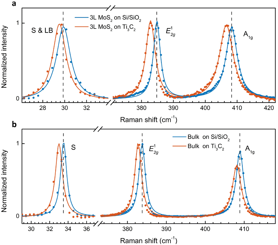 | ||
| Fig. 4 Raman spectra of 3L (a) and bulk (b) MoS2 on Ti3C2 MXene in comparison with the counterparts on Si/SiO2. | ||
The A1g mode in 3L and bulk also red-shifts by a slightly smaller magnitude compared to the E12g mode (1.7 cm−1vs. 2.0 cm−1 in 3L; 0.8 cm−1vs. 1.1 cm−1 in bulk). Note that the shift rate varies as a function of thickness. Experimentally, Hui et al. demonstrated that the shift ratio of E12g to A1g is ∼1.5 in 3L under biaxial strain.39 If we use the E12g mode to determine the strain value, the strain-induced shift of the A1g mode should be 1.3 cm−1, smaller than the observed shift of 1.7 cm−1. The additional redshift of 0.4 cm−1 could be attributed to the electron doping effect, similar to the analysis for 1L. Although the line width of the A1g peak shows negligible change, different from that in 1L, the doping-induced redshift of 0.4 cm−1 in 3L is much smaller than that in 1L (1.9 cm−1). As a result, the line width is hardly affected due to the smaller doping density. The doping effect in 3L MoS2 is also confirmed from the PL spectra (Fig. S2†).
Discussion on the possible laser heating effect
The laser power we used for the above measurements was 0.5 mW, which is not large for MoS2. Nonetheless, we conducted excitation power-dependent measurements on another sample with laser power ranging from 0.05 mW to 0.7 mW. As shown in Fig. 5, the E12g mode exhibits a constant peak position for 1L MoS2 on Si/SiO2, while the maximum redshift from the A1g peak is ∼0.2 cm−1, which is within the resolution of our measurements. This indicates that the laser heating effect is negligible. However, it is surprising to see that both peaks red-shift substantially as a function of power for 1L MoS2 on Ti3C2 MXene. Considering that the thermal conductivity of Ti3C2 MXene is higher than that of SiO2,40,41 heat dissipation should be effective via the Ti3C2 MXene layer. Nevertheless, the laser-induced redshifts indicate that the Ti3C2 MXene layer absorbs more heat upon laser illumination, resulting in a smaller temperature gradient and thus less effective heat transfer. We note that the power-induced shifts in both Raman peaks and PL emission are reversible (Fig. S3†), which further supports the heating effect. | ||
| Fig. 5 Raman peak positions as a function of excitation power. (a and b) Peak positions of the E12g (a) and A1g (b) modes. Dots represent experimental data and lines correspond to a linear fitting. | ||
As both A1g and E12g modes soften linearly without saturation, the absence of nonlinear effects indicates that the laser-induced shifts are linear below 0.7 mW.42 Therefore, we used ω(P) = ω0+ χp(P) to fit the power-dependent peak positions. Here, P is the excitation power, ω0 is the intrinsic peak position without heating effects, and χp is the power coefficient. For 1L MoS2 on Ti3C2 MXene, we found that χp = −3.0 cm−1 and ω0 = 386.1 cm−1 for the E12g mode, and χp = −4.2 cm−1 and ω0 = 406.0 cm−1 for the A1g mode (Fig. 5, red). The extracted power coefficients are much larger than those from Si/SiO2-supported (Fig. 5, blue) and sapphire-supported MoS2,42 but smaller than the values observed for suspended monolayer MoS2.42 After subtracting the heat-induced shift, we still obtained a redshift of 0.4 cm−1 for the E12g mode in 1L MoS2, which corresponds to 0.08% strain. Such a small in-plane strain causes a negligible shift in the A1g mode, which implies that the 0.8 cm−1 shift (corrected after subtracting the heating effect) for the A1g mode is mainly due to the electron doping effect. We note that using the lowest excitation power is not necessarily the best method for measurements since destructive interference from the substrate may lower the Raman intensity and affect the signal-to-noise ratio.11 Instead, performing a detailed power-dependent measurement in the low and moderate range should be appropriate to subtract the laser heating effect. In addition to 1L MoS2, we further conducted power-dependent Raman scattering and PL measurements on 3L MoS2 (Fig. S4 and S5†), which also corroborate the laser heating effect. Additionally, the temperature-dependent shifts of E12g and A1g modes from 150 K to 300 K are shown in Fig. S6,† where both peaks shift linearly, consistent with the power-dependent measurements.
Conclusions
In summary, our work demonstrates the substrate effect of Ti3C2 MXene on MoS2 in Raman spectroscopy. Compared to MoS2 on Si/SiO2, we observed redshifts of the fingerprint peaks from MoS2 on Ti3C2 MXene and explained these shifts based on the vibrational nature of each peak. The in-plane E12g mode is more sensitive to strain which arises from both sample fabrication and lattice mismatch, but a small variation in strain hardly shifts the out-of-plane A1g mode. We attributed the down-shifted A1g mode to the electron doping effect, which is also confirmed by the suppressed and red-shifted PL emission. In addition to the monolayer, we showed that the modulation from Ti3C2 MXene is also present in few-layer and bulk MoS2.Furthermore, we demonstrate that laser excitation power plays a vital role in determining the external perturbations and the magnitude of the heat-induced redshifts varies depending on the underlying substrate. As Raman spectroscopy has been widely used as a nondestructive tool to identify strain and doping effects,43–45 our results show that a careful power-dependent measurement is essential to subtract the laser-induced shifts and extract the pure modulation from the substrate.
Our work contributes to the understanding of interfacial interaction between Ti3C2 MXene and MoS2 and also provides some insights into the application of MoS2–Ti3C2 heterostructures. While the local heating effect from Ti3C2 MXene could potentially deteriorate the performance of MoS2–Ti3C2 MXene in nanoelectronics, the Ti3C2 MXene-induced strain and doping, on the other hand, may improve the performance of MoS2 as an electrocatalyst in the hydrogen evolution reaction.46
Methods
Synthesis of Ti3C2 MXene free-standing paper
A solution of 9 M hydrochloric acid (HCl) and 7.5 M potassium fluoride (KF) was prepared as the etching solution. 4 g of Ti3AlC2 was added slowly to 80 mL of the solution and stirred at 35 °C for 48 h using magnetic stirring in an oil bath for uniform heating. Subsequently, the solution was washed until the pH level was near neutral. The supernatant was discarded, leaving purified MXene as sediment. DI water was added to it, followed by shaking, and vacuum-filtration.For delamination, 1 g of Ti3C2 MXene was added to 35 mL of 5 M LiCl, shaken manually for a minute, and left to soak for 24 h at room temperature. The mixture was centrifuged, and the supernatant was decanted to remove concentrated LiCl. Fresh DI water was added for washing followed by centrifugation and discarding the supernatant. The washing process was repeated three times. After washing, DI water was added, and the mixture was bath sonicated for 1 h followed by centrifugation at 5000 rpm for 1 h. The supernatant was collected and DI water was again added, followed by repeated sonication and centrifugation, until a clear supernatant was obtained. The collected supernatants were combined, shaken and vacuum-filtered to make a free-standing MXene paper. The Ti3C2 MXene multilayers were produced by mechanical exfoliation from the MXene paper. The Raman spectrum of Ti3C2 MXene paper is shown in Fig. S7,† and the Energy Dispersive Spectroscopy (EDS) mapping image of the exfoliated flakes is shown in Fig. S8.†
Raman and PL spectroscopy measurements
We carried out the optical measurement by using a home-built setup. The measurements were conducted in a backscattering configuration, excited with a 532 nm laser. The excitation power was kept at 0.5 mW for Fig. 2–4 and varied between 0.05 mW and 0.7 mW for the laser heating effect study (Fig. 5). To reach a low-frequency Raman shift of ∼10 cm−1, we used volume Bragg grating filters (OptiGrate) to block the laser line. The backscattered signal was collected through a 100× objective and dispersed by an 1800 g mm−1 (Raman) or 300 g mm−1 (PL) grating before being detected by a liquid nitrogen-cooled charge coupled device (Princeton Instruments, PyLoN 1340 × 400 pixels CCD). The spectral resolution of our Raman spectroscopy measurements is ∼0.7 cm−1. Except for the temperature-dependent measurements, all spectra were taken at room temperature.Data availability
The data that support the findings of this work are available in the manuscript and its ESI.†Author contributions
Conceived and designed the experiments: X. L., Q. Z. and M. N. Sample fabrication: E. P., E. L., K. A., A. M., F. W., A. S. and M. B. Data acquisition: E. P., Q. Z. and K. A. Data analysis: X. L., E. P., Q. Z. and M. N. Writing – original draft: X. L., E. P. and Q. Z. Writing – review & editing: X. L., E. P., Q. Z. M.N. and E. L. All authors reviewed the manuscript.Conflicts of interest
There are no conflicts to declare.Acknowledgements
Acknowledgment is made to the donors of the American Chemical Society Petroleum Research Fund for partial support of this research. X. L. acknowledges support from the Tulane University startup fund. A. M., E. L. and M. N. were supported by the National Science Foundation under Grant No. DMR-2048164.References
- B. Anasori and M. Naguib, MRS Bull., 2023, 48, 238–244 CrossRef CAS.
- M. R. Lukatskaya, O. Mashtalir, C. E. Ren, Y. Dall'Agnese, P. Rozier, P. L. Taberna, M. Naguib, P. Simon, M. W. Barsoum and Y. Gogotsi, Science, 2013, 341, 1502–1505 CrossRef CAS PubMed.
- J. Zhang, Y. Zhao, X. Guo, C. Chen, C.-L. Dong, R.-S. Liu, C.-P. Han, Y. Li, Y. Gogotsi and G. Wang, Nat. Catal., 2018, 1, 985–992 CrossRef CAS.
- Z. Wang, H. Kim and H. N. Alshareef, Adv. Mater., 2018, 30, 1706656 CrossRef PubMed.
- Y. Ma, N. Liu, L. Li, X. Hu, Z. Zou, J. Wang, S. Luo and Y. Gao, Nat. Commun., 2017, 8, 1207 CrossRef PubMed.
- B. Xu, M. Zhu, W. Zhang, X. Zhen, Z. Pei, Q. Xue, C. Zhi and P. Shi, Adv. Mater., 2016, 28, 3333–3339 CrossRef CAS PubMed.
- H. Kim, Z. Wang and H. N. Alshareef, Nano Energy, 2019, 60, 179–197 CrossRef CAS.
- X. Xu, T. Guo, M. K. Hota, H. Kim, D. Zheng, C. Liu, M. N. Hedhili, R. S. Alsaadi, X. Zhang and H. N. Alshareef, Adv. Mater., 2022, 34, 2107370 CrossRef CAS PubMed.
- N. H. Attanayake, S. C. Abeyweera, A. C. Thenuwara, B. Anasori, Y. Gogotsi, Y. Sun and D. R. Strongin, J. Mater. Chem. A, 2018, 6, 16882–16889 RSC.
- A. Macknojia, A. Ayyagari, D. Zambrano, A. Rosenkranz, E. V. Shevchenko and D. Berman, ACS Nano, 2023, 17, 2421–2430 CrossRef CAS PubMed.
- M. Buscema, G. A. Steele, H. S. Van Der Zant and A. Castellanos-Gomez, Nano Res., 2014, 7, 561–571 CrossRef.
- S. Tongay, W. Fan, J. Kang, J. Park, U. Koldemir, J. Suh, D. S. Narang, K. Liu, J. Ji and J. Li, Nano Lett., 2014, 14, 3185–3190 CrossRef CAS PubMed.
- C. H. Lui, Z. Ye, C. Ji, K.-C. Chiu, C.-T. Chou, T. I. Andersen, C. Means-Shively, H. Anderson, J.-M. Wu and T. Kidd, Phys. Rev. B:Condens. Matter Mater. Phys., 2015, 91, 165403 CrossRef.
- H. Fang, C. Battaglia, C. Carraro, S. Nemsak, B. Ozdol, J. S. Kang, H. A. Bechtel, S. B. Desai, F. Kronast and A. A. Unal, Proc. Natl. Acad. Sci. U.S.A., 2014, 111, 6198–6202 CrossRef CAS PubMed.
- K.-G. Zhou, F. Withers, Y. Cao, S. Hu, G. Yu and C. Casiraghi, ACS Nano, 2014, 8, 9914–9924 CrossRef CAS PubMed.
- H. Li, J.-B. Wu, F. Ran, M.-L. Lin, X.-L. Liu, Y. Zhao, X. Lu, Q. Xiong, J. Zhang and W. Huang, ACS Nano, 2017, 11, 11714–11723 CrossRef CAS PubMed.
- A. Castellanos-Gomez, M. Buscema, R. Molenaar, V. Singh, L. Janssen, H. S. Van Der Zant and G. A. Steele, 2D Mater., 2014, 1, 011002 CrossRef CAS.
- F. Pizzocchero, L. Gammelgaard, B. S. Jessen, J. M. Caridad, L. Wang, J. Hone, P. Bøggild and T. J. Booth, Nat. Commun., 2016, 7, 11894 CrossRef CAS PubMed.
- H. Zhang, Y. Ma, Y. Wan, X. Rong, Z. Xie, W. Wang and L. Dai, Sci. Rep., 2015, 5, 8440 CrossRef CAS PubMed.
- X. Lu, M. I. B. Utama, J. Zhang, Y. Zhao and Q. Xiong, Nanoscale, 2013, 5, 8904–8908 RSC.
- C. Lee, H. Yan, L. E. Brus, T. F. Heinz, J. Hone and S. Ryu, ACS Nano, 2010, 4, 2695–2700 CrossRef CAS PubMed.
- X. Luo, Y. Zhao, J. Zhang, Q. Xiong and S. Y. Quek, Phys. Rev. B:Condens. Matter Mater. Phys., 2013, 88, 075320 CrossRef.
- Q.-H. Tan, X. Zhang, X.-D. Luo, J. Zhang and P.-H. Tan, J. Semicond., 2017, 38, 031006 CrossRef.
- T. Wieting and J. Verble, Phys. Rev. B:Condens. Matter Mater. Phys., 1972, 5, 1473 CrossRef.
- P. N. Ghosh and C. Maiti, Phys. Rev. B:Condens. Matter Mater. Phys., 1983, 28, 2237 CrossRef CAS.
- Y. Lin, X. Ling, L. Yu, S. Huang, A. L. Hsu, Y.-H. Lee, J. Kong, M. S. Dresselhaus and T. Palacios, Nano Lett., 2014, 14, 5569–5576 CrossRef CAS PubMed.
- X. Lu, X. Luo, J. Zhang, S. Y. Quek and Q. Xiong, Nano Res., 2016, 9, 3559–3597 CrossRef CAS.
- X. Zhang, X.-F. Qiao, W. Shi, J.-B. Wu, D.-S. Jiang and P.-H. Tan, Chem. Soc. Rev., 2015, 44, 2757–2785 RSC.
- X. Zhang, Q.-H. Tan, J.-B. Wu, W. Shi and P.-H. Tan, Nanoscale, 2016, 8, 6435–6450 RSC.
- H. J. Conley, B. Wang, J. I. Ziegler, R. F. Haglund Jr, S. T. Pantelides and K. I. Bolotin, Nano Lett., 2013, 13, 3626–3630 CrossRef CAS PubMed.
- D. Lloyd, X. Liu, J. W. Christopher, L. Cantley, A. Wadehra, B. L. Kim, B. B. Goldberg, A. K. Swan and J. S. Bunch, Nano Lett., 2016, 16, 5836–5841 CrossRef CAS PubMed.
- B. Chakraborty, A. Bera, D. Muthu, S. Bhowmick, U. V. Waghmare and A. Sood, Phys. Rev. B:Condens. Matter Mater. Phys., 2012, 85, 161403 CrossRef.
- X. Lu, M. I. B. Utama, X. Wang, W. Xu, W. Zhao, M. H. S. Owen and Q. Xiong, Small, 2017, 13, 1701039 CrossRef PubMed.
- J.-U. Lee, J. Park, Y.-W. Son and H. Cheong, Nanoscale, 2015, 7, 3229–3236 RSC.
- Y. Li, Z. Qi, M. Liu, Y. Wang, X. Cheng, G. Zhang and L. Sheng, Nanoscale, 2014, 6, 15248–15254 RSC.
- G. Berdiyorov, AIP Adv., 2016, 6, 055105 CrossRef.
- K. F. Mak, K. He, C. Lee, G. H. Lee, J. Hone, T. F. Heinz and J. Shan, Nat. Mater., 2013, 12, 207–211 CrossRef CAS PubMed.
- J.-U. Lee, S. Woo, J. Park, H. C. Park, Y.-W. Son and H. Cheong, Nat. Commun., 2017, 8, 1370 CrossRef PubMed.
- Y. Y. Hui, X. Liu, W. Jie, N. Y. Chan, J. Hao, Y.-T. Hsu, L.-J. Li, W. Guo and S. P. Lau, ACS Nano, 2013, 7, 7126–7131 CrossRef CAS PubMed.
- S. Callard, G. Tallarida, A. Borghesi and L. Zanotti, J. Non-Cryst. Solids, 1999, 245, 203–209 CrossRef CAS.
- P. Yasaei, Z. Hemmat, C. J. Foss, S. J. Li, L. Hong, A. Behranginia, L. Majidi, R. F. Klie, M. W. Barsoum and Z. Aksamija, Adv. Mater., 2018, 30, 1801629 CrossRef PubMed.
- R. Yan, J. R. Simpson, S. Bertolazzi, J. Brivio, M. Watson, X. Wu, A. Kis, T. Luo, A. R. Hight Walker and H. G. Xing, ACS Nano, 2014, 8, 986–993 CrossRef CAS PubMed.
- M. Velicky, A. Rodriguez, M. Bousa, A. V. Krayev, M. Vondracek, J. Honolka, M. Ahmadi, G. E. Donnelly, F. Huang and H. D. Abruna, J. Phys. Chem. Lett., 2020, 11, 6112–6118 CrossRef CAS PubMed.
- M. O'Brien, N. Scheuschner, J. Maultzsch, G. S. Duesberg and N. McEvoy, Phys. Status Solidi B, 2017, 254, 1700218 CrossRef.
- Y. Wang, J. Balgley, E. Gerber, M. Gray, N. Kumar, X. Lu, J.-Q. Yan, A. Fereidouni, R. Basnet and S. J. Yun, Nano Lett., 2020, 20, 8446–8452 CrossRef CAS PubMed.
- S. Bolar, S. Shit, N. C. Murmu, P. Samanta and T. Kuila, ACS Appl. Mater. Interfaces, 2021, 13, 765–780 CrossRef CAS PubMed.
Footnote |
| † Electronic supplementary information (ESI) available. See DOI: https://doi.org/10.1039/d5na00096c |
| This journal is © The Royal Society of Chemistry 2025 |