DOI:
10.1039/D4NA01048E
(Paper)
Nanoscale Adv., 2025,
7, 1989-2002
A comparative study of the hot electron energy loss rate in zinc- and cadmium compound quasi-two-dimensional materials
Received
18th December 2024
, Accepted 26th January 2025
First published on 17th February 2025
Abstract
In this paper, a comparative study of the electron energy loss rate (ELR) in zinc-based chalcogenide (ZnS, ZnSe, and ZnTe) and cadmium-based chalcogenide (CdS, CdSe, and CdTe) quantum wells owing to interaction with optical phonons in a quantising magnetic field is carried out by employing the electronic temperature model. The dependence of the electron ELR on the material slab thickness, quantizing magnetic field, surface electronic concentration, and electronic temperature in ZnS, ZnSe, and ZnTe as well as in CdS, CdSe, and CdTe materials is obtained and compared in detail. Our findings offer valuable information for the advancement of electronic devices.
1. Introduction
As material technology continues to advance, the investigation of low-dimensional electron systems plays a crucial role in semiconductor physics. The way electrons behave in these systems is influenced by how they interact with other electrons, impurities, and phonons. Among them, the electron–phonon interaction is a significant mechanism that impacts the electrical transport characteristics in polar semiconductors.1–3 This interaction in confined 2D systems has received significant interest recently due to its fundamental role in the relaxation of carriers under conditions with hot electrons.4–6 Recently, interest has increased dramatically in the fascinating subject of hot electron relaxation in 2D systems. This phenomenon has captured the attention of researchers and scientists, leading to enthusiastic experimental and theoretical investigations.7,8 Understanding the reasons for energy loss is crucial due to its technological significance, given that the majority of semiconductor devices function under high-field conditions. When a strong electric field is applied, the temperature of the electron gas rises above that of the surrounding lattice. Then, the electron and lattice reach equilibrium by emitting various types of phonons, depending on the temperature region.9 At temperatures below a certain threshold (below 50 K), the main method by which temperature decreases is through emitting acoustic phonons via deformation potential coupling. Conversely, at more elevated temperatures (above 50 K), the primary method by which electrons lose heat is through emitting optical phonons.10–12 Therefore, the investigation of energy loss mechanisms in hot carriers can be utilized as a probe to explore the mechanisms of e–p interaction in 2D nanostructures.
Semiconductor materials with exceptional properties at the nanostructure level have garnered significant interest for use in various devices such as energy storage devices, photovoltaic solar cell technologies, electronic devices, light-emitting diodes, field-effect transistors, sensors, and more.13,14 Semiconductors have a band gap that falls between that of insulators and metals. They are mainly categorized into three groups: inorganic semiconductors, for instance, metal oxides; organic semiconductors, for instance, conjugated polymers; and organic–inorganic semiconductors, for instance, nanoparticle-polymer composites. In this context, inorganic semiconductors were discovered as a promising group of materials due to their superior carrier mobility and high stability. Organic semiconductors are inexpensive, flexible, and lightweight. Hybrid inorganic–organic semiconductors benefit from the synergistic interplay between inorganic and organic semiconductors, offering the potential for the high processability of organic semiconductors and the excellent carrier mobility of inorganic semiconductors. The continued progress of nanotechnology is expected to result in important advancements in the semiconductor industry.
It is possible to fabricate semiconductor nanostructures via self-organization employing heteroepitaxial growth, a process in which material 1 is grown on a substrate of a different material, material 2. During heteroepitaxial growth, the two materials' lattice constants frequently differ. The categorization of semiconductor nanostructures is based on nanocrystalline materials, where the electrons are restricted to areas with three, two, or one dimension when the nanostructure's relative dimension is similar to the de Broglie wavelength. The de Broglie wavelength of free carriers in semiconductor CdSe is approximately 10 nm. Semiconductor crystal nanostructures with a z-direction below this critical value, such as quantum wells (QWs), layer structures, and thin films, are categorized as 2D nanostructures.15,16 QW nanostructures have garnered significant attention, due to their unique mechanical, electrical, and optic characteristics, as well as their potential uses across various industries.17 The focus on nanostructures arises because particles moving within small crystals experience quantization, known as the quantum confinement effect. It is known that today we possess advanced techniques for creating QW nanostructures. They are laser ablation, ion implantation, and molecular beam epitaxy. Lately, advanced nanofabrication techniques have led to the development of freestanding QW nanostructures, offering the potential to observe the confinement effects in a quantum plane.18 We are employing the freestanding QW nanostructure with a square-confined potential in this work, because in addition to the effects of the quantizing magnetic field, the electronic effective temperature, and the surface electronic concentration on the hot electron ELR, the well-width or material slab thickness also greatly influences the hot electron ELR. Almost all of the physical properties, including dielectric, magnetic, thermal, optical, structural, and more of QW nanostructures are greatly affected by the size reduction due to the quantum size effects and surface effects. Due to their incredibly small dimensions, these nanostructures display characteristics that are fundamentally distinct from, and frequently better than, those of their traditional equivalent. In recent times, there has been significant focus on investigating the quantum size effect in semiconductors with decreased dimensions (on nanometer size) because of their utility in magnetic sensors, single electron devices, catalysis, memory devices, optoelectronic devices, resonant tunneling devices, and other applications.19–24
Nowadays, wide-bandgap semiconductors are gaining a lot of attention in technology due to their prospective applications in high-temperature, high-powder devices as well as the demand for optic materials with activity in the blue green spectrum. Among such materials, ZnTe, ZnSe, and ZnS are members of the IIB–VIA compound family of wide-bandgap semiconductors, crystallising at room temperature and pressure in a cubic zinc blende structure.25–27 As blue-lasing materials, they have drawn a lot of interest and could be applied in the creation of optical waveguides and modulated heterostructures.28 When doped with Mn, they have also shown to be very intriguing diluted semiconductors.29 When combined with other elements such as BCC iron, cobalt, manganese, and nickel, they may even be utilised as microelectronic magnetic materials.30 In addition to silicon (Si) and III–V compounds like GaAs, II–VI compounds like compound semiconductors based on zinc (Zn) and cadmium (Cd) can all be used to create solar cells.31 Cadmium chalcogenides (CdS, CdSe, and CdTe) have garnered significant attention in recent times due to their exceptional characteristics, including the changeable range of light absorption and effective charge separation.32 CdTe, CdSe, and CdS are materials with a direct bandgap. The bulk bandgaps of CdTe, CdSe, and CdS are 1.49, 1.74, and 2.4 eV, respectively.33 Among them, the p-type semiconductor is CdTe, whereas the n-type ones are CdS and CdSe. CdTe is the most alluring of these semiconductors due to its benefits:31,33 Firstly, at room temperature, the direct-bandgap semiconductor CdTe has a band gap of 1.49 eV. This is near the optimal value for solar cells as determined theoretically. Secondly, since a layer as thin as 2 μm absorbs about 90% of incident light due to CdTe's high absorption coefficient, less semiconductor material is required overall compared to Si, which absorbs about 10 μm. As a result, a low-cost material that has shown the greatest potential for highly efficient solar cells in photovoltaic systems is CdTe.
The comprehension of mechanisms causing energy loss is crucial due to its technological significance since the majority of semiconductor devices are currently used under high field conditions. The use of a quantized magnetic field in a 2D nanostructure adds an intriguing dimension to the relaxation of hot electrons. It is widely accepted that the existence of a magnetic-field applied perpendicular to a 2D nanostructure layer results in a significant change in the e–ph interaction resulting from the quantization of the carrier's energy in the 2D plane. In the presence of a magnetic-field that causes quantization, the energy levels of carriers that interact with phonons are significantly changed, resulting in a modification of the rate at which energy is released.34 In the literature, there have been some investigations of hot electron ELR in nanostructures in a quantized magnetic field.9,11,35–37 However, in these reports, the authors have mainly focussed on GaAs material, and simultaneously, the effects of surface electronic concentration and 2D material slab thickness on the hot electron ELR have not yet been considered in detail. Except for a recent calculation by J. S. Bhat, B. G. Mulimani, and R. A. Nesargi,11 where hot electron ELR owing to acoustic phonon interaction based on deformation potential was computed for the four materials GaAs, GaN, InAs, and InSb. Their results displayed that the electron ELR depends on the electronic effective TE and the quantizing BQ. Concurrently, their results also represented that the electron ELR in various materials is very different. Consequently, their results provide useful insights into the nanoscale domain for the advancement of optoelectronic devices, because InAs, InSb, GaAs, and GaN compound materials are popularly used in optoelectronic device fabrication.
It is well-known that, in addition to InAs, InSb, GaAs, and GaN compound semiconductors, II–VI compounds like compound semiconductors based on zinc (Zn) and cadmium (Cd) such as zinc chalcogenides (ZnS, ZnSe, and ZnTe) and cadmium chalcogenides (CdS, CdSe, and CdTe) also are extensively utilized in optoelectronic device fabrication in the nanoscale regime, especially in solar cell fabrication. This is also mentioned above and shown clearly in ref. 31. In these optoelectronic devices, the excited electrons experience relaxation via optical or acoustic phonon emission. Simultaneously, when nanostructure devices operate under high field settings, their efficiency is impacted directly by the energy relaxation rate.11 Thus, to enhance the efficiency of nanostructure optoelectronic devices, conducting a comparative study of hot electron ELR in zinc- and cadmium-compound two-dimensional materials, such as ZnS, ZnSe, ZnTe, CdS, CdSe, and CdTe is necessary and of scientific and technological interest.
In this work, a comparative study of the hot electron ELR in zinc-based chalcogenides (ZnS, ZnSe, and ZnTe) and cadmium based chalcogenides (CdS, CdSe, and CdTe) owing to interaction with optical phonons in a quantizing BQ is carried out by employing the electronic temperature model. In Section 2, we provide the basic formalisms of the electronic temperature and Q2D electronic system models. Section 3 presents the analytical calculation results for the hot electron ELR in Zn X and Cd X (X = Se, Te, and S) 2D nanostructure materials owing to interaction with optical phonons in a quantizing B. Section 4 presents the outcomes of the numerical computations displayed for zinc-based chalcogenide (ZnS, ZnSe, and ZnTe) and cadmium-based chalcogenide (CdS, CdSe, and CdTe) semiconductors. Finally, conclusions are presented in Section 5.
2. Basic formalism and analytical results
2.1. Electron temperature model
In this study, the electron temperature (TE) model7,8 is applied to calculated the electron ELR. The electrons in this particular model are characterized by a Fermi–Dirac distribution function with an electronic temperature (which is denoted as  ) that is greater than the lattice temperature (which is denoted as
  ). In this case, the average energy loss rate,
  , takes the form of7–9
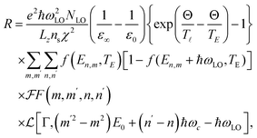
| |  | (1) |
where q = (q⊥, qz) is the wave-vector of phonons, ℏωq is the phonon energy, Nq is the Bose distribution function, and Ne is the number of electrons. The factor, ∂Nq/∂t, takes the form of9| |  | (2) |
where the electron scattering rate due to optical phonon absorption or emission is represented by PA or PE, respectively, and the Fermi–Dirac distribution function at temperature TE of the electron in the initial (i)/final (f) state is represented by f(Ei(f), TE). Then, the electron scattering rate is described by the following Fermi golden rule:| |  | (3) |
where the Hamiltonian for the e–optical-p interaction is denoted by He−p.
2.2. Quasi-two dimensional electron system model
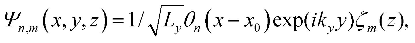
In this research, we consider a 2D electron–phonon system in a QW, which is made of zinc-based chalcogenide (ZnS, ZnSe, and ZnTe) and cadmium-based chalcogenide (CdS, CdSe, and CdTe) semiconductors. Here, the magnetic field B is in the system's z-direction, and carriers move freely in the system's (x, y)-plane. Then, the 2D electron's corresponding eigenvalue (En,m) and eigenfunction (Ψn,m) are given by38| |  | (4) |
| |  | (5) |
where, the y-axis wave vector is represented as ky, the normalization length is represented as Ly, and the harmonic oscillator function is represented as θn(x − x0) with x0 = −χ2ky. Here χ = {ℏc/(|e|B)}1/2 and  are the cyclotron-radius and -frequency, n = 0, 1, 2, 3, 4, … denotes the Landau levels (LLs), m = 1, 2, 3, 4, … represents the electric sub-band levels, and
  is the energy of the lowest electric subband, with Lz referring to the well-width or material slab thickness. In the case of 2D electrons in zinc-based chalcogenides (ZnS, ZnSe, and ZnTe) and cadmium-based chalcogenides (CdS, CdSe, and CdTe) semiconductors are confined via V(z)-potential:39–41
| |  | (6) |
then, the wave-function ζm(z) of 2D-electrons in the nanostructure along the QW's z-axis has the form:| |  | (7) |
2.3. Electron–optical phonon interaction in a quantizing magnetic field
In this study, we consider the coupling of LO phonons to an electron in a 2D nanostructure in a quantizing B. Then, the Fröhlich Hamiltonian describes the interaction Hamiltonian (Hel–ph) for an electron that interacts with LO-phonons as follows:42| |  | (8) |
where| |  | (9) |
here the creation  and annihilation (bq) operators of an optical phonon with wave vector (q), position vector (r), and energy (ℏωLO) are mentioned. The el–ph coupling constant in this 2D electron system is denoted by λ. Based on the electron temperature model, the expression for the electron ELR caused by optical phonons in a 2D nanostructure is derived as follows:
| |  | (10) |
where e, NLO, ns, and Lz are the electron's charge, the LO-phonon's Bose distribution function, the material's surface concentration, and the material slab thickness, respectively. Besides, q⊥ = (qx, qy) and Θ = ℏωLO/kB. The high  and static
  frequency dielectric constants are also mentioned. The factor |Jn,n′(q⊥)|2 is delineated by
| |  | (11) |
where n1 = max(n′, n) while n2 = min(n′, n), and  represents the Laguerre polynomials. In addition, the factor
 , represents the following overlap integral
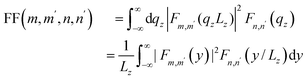
| | 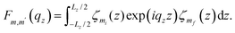 | (12) |
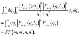
To obtain the electron ELR's explicit expression in eqn (10), we have to carry out a detailed evaluation of the following integral
| |  | (13) |
The evaluation process is as follows:
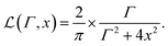
From eqn (13), we can see that the delta Dirac function is not dependent on q⊥ and qz. Therefore, it can be approximated by a Lorentz function with the Γ width as follows:
| |  | (14) |
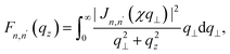
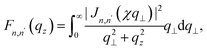
Setting Fn,n′(qz) using the following integral
| |  | (15) |
we have
| |  | (16) |
Then, the electron ELR's expression in
eqn (10) can be rewritten as
| |  | (17) |
where
| |  | (18) |
with
| |  | (19) |
Noting that the integral,
Fn,n′(
qz),
| |  | (20) |
can be evaluated based on the following Gauss–Laguerre expression
| |  | (21) |
here
xi (
i = 1, …,
k) represents the zeroes of the Laguerre polynomials
LX(
X):
LX(
X) = 0, and
ωi is given by
| |  | (22) |
and then
| |  | (23) |
wherefore, we obtain
| |  | (24) |
Moreover, the integral , in eqn (18)
| |  | (25) |
can be evaluated based on the following Gauss–Hermite integral:
| |  | (26) |
where
yi (
i = 1, …,
k) represents the zeroes of the Hermite polynomials

:

, and
ωi is given by
| |  | (27) |
and then,
| |  | (28) |
Finally, we obtain
| |  | (29) |
Appropriate computational methods will be applied to the analytically computed outcomes mentioned above to obtain the numerical analysis results and visual representations. The reliable results for the comparative study of hot electron ELR in zinc- and cadmium-compound two-dimensional materials, influenced by optical phonons in a quantizing BQ, will be presented in the subsequent section.
3. Numerical results and discussion
The numerical evaluation outcomes for the comparative study of hot electron ELR in zinc- and cadmium-compound 2D materials presented in this section are intended to encompass: (i) comparing the quantizing BQ dependence of the electron ELR between Zn X and Cd X materials (where X = Te, S, and Se) when interacting with optical phonons. (ii) Comparing the surface concentration dependence of the electron ELR between Zn X and Cd X when interacting with optical phonons. (iii) comparing the quantizing BQ dependence of the electron ELR between Zn X and Cd X when interacting with optical phonons at various effective temperatures, namely, TE = 150 K, TE = 200 K, and TE = 300 K. (iv) Comparing the electronic effective temperature dependence of the electron ELR between Zn X and Cd X when interacting with optical phonons at various slab thicknesses, namely, Dz = 10 nm, Dz = 12 nm, and Dz = 14 nm. (v) Comparing the electronic effective temperature dependence of the electron ELR between Zn X and Cd X when interacting with optical phonons. (vi) Comparing the material slab thickness dependence of the electron ELR between Zn X and Cd X when interacting with optical phonons at various effective temperatures, namely, TE = 100 K, TE = 200 K, and TE = 300 K. (vii) Comparing the material slab thickness dependence of the electron ELR between Zn X and Cd X when interacting with optical phonons. The detailed outcomes are shown in the figures below Table 1.
Table 1 The parameters of zinc- and cadmium-compound Q2D materials (ZnSe, ZnTe, ZnS, CdSe, CdTe, and CdS) used in calculations:43
| Parameters |
ZnSe |
ZnTe |
ZnS |
CdSe |
CdTe |
CdS |
 ( × m0) ( × m0) |
0.14 |
0.13 |
0.34 |
0.12 |
0.09 |
0.14 |
|
ϵ
0
|
7.60 |
9.67 |
8.00 |
10.16 |
10.20 |
8.45 |
|
ϵ
∞
|
5.40 |
7.28 |
5.10 |
6.20 |
7.10 |
5.32 |
|
ℏω
LO (meV) |
31.40 |
25.60 |
43.20 |
25.90 |
21.00 |
37.30 |
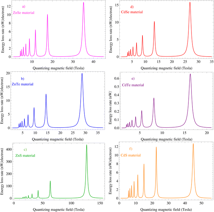
The graphical representations in Fig. 1 show the numerical evaluation outcomes of comparing the quantizing BQ dependence of the electron ELR between Zn X and Cd X materials (X = Te, S, and Se) when interacting with optical phonons. Here, the lattice temperature, T![[small script l]](https://www.rsc.org/images/entities/char_e146.gif) = 4.2 K, the electronic effective temperature, TE = 77 K, the surface concentration, Ns = 2 × 10¹⁵ m−2, and the material slab thickness, Lz = 7 nm. The data presented in Fig. 1a–f correspond to ZnSe, ZnTe, ZnS, CdSe, CdTe, and CdS materials. Via the optical phonon emission, a confined electron in ZnSe, ZnTe, ZnS, CdSe, CdTe, and CdS materials can transfer resonantly between LLs, result in the emergence of resonance peaks. More specifically, the resonance condition nℏωc = ℏωLO, or in other words,
= 4.2 K, the electronic effective temperature, TE = 77 K, the surface concentration, Ns = 2 × 10¹⁵ m−2, and the material slab thickness, Lz = 7 nm. The data presented in Fig. 1a–f correspond to ZnSe, ZnTe, ZnS, CdSe, CdTe, and CdS materials. Via the optical phonon emission, a confined electron in ZnSe, ZnTe, ZnS, CdSe, CdTe, and CdS materials can transfer resonantly between LLs, result in the emergence of resonance peaks. More specifically, the resonance condition nℏωc = ℏωLO, or in other words,  is satisfied. In the case where n = 1, the resonance peak in the electron ELR graph occurs for ZnSe, ZnTe, ZnS, CdSe, CdTe, and CdS materials at the following quantizing magnetic fields: BQ = 35.22 T, BQ = 28.72 T, BQ = 126.74 T, BQ = 26.82 T, BQ = 16.31 T, and BQ = 45.06 T, respectively. Similarly, in the case where n = 2, the resonance peak in the electron ELR graph occurs for ZnSe, ZnTe, ZnS, CdSe, CdTe, and CdS materials at the following quantizing magnetic fields: BQ = 17.61 T, BQ = 14.36 T, BQ = 63.37 T, BQ = 13.41 T, BQ = 8.15 T, and BQ = 22.53 T, respectively; this pattern continues for higher levels when n = 3 and so on. In general, when a quantizing BQ is present, a confined electron transitions resonantly between the LLs by emission or absorption of suitable optical phonon energy in zinc-based chalcogenides (ZnS, ZnSe, and ZnTe) and cadmium-based chalcogenides (CdS, CdSe, and CdTe). In this process of magneto-phonon resonance (MPR) effect, the energy discrepancy between the final and initial electronic states is equal to the energy of the optical phonon. The associated relaxation time in Zn X and Cd X materials (X = Te, S, and Se) will be reduced, and the scattering rate in these materials will increase, resulting in the appearance of resonance peaks in the electron ELR graph as a function of the quantizing magnetic field. In the figures, the rate of electron scattering changes depending on the energy range of optical phonons in ZnSe, ZnTe, ZnS, CdSe, CdTe, and CdS materials. Under a specific magnetic field, the energy of the optical phonon aligns perfectly for a transition between LLs, resulting in a maximum relaxation rate. It is fascinating to observe the discrepancies in the electron ELR across various materials in zinc-based chalcogenide (ZnS, ZnSe, and ZnTe) and cadmium-based chalcogenide (CdS, CdSe, and CdTe) 2D materials in this study. In the figure, the electron ELR graphs show that the amplitudes of the MPR oscillations in ZnSe, ZnTe, ZnS, CdSe, CdTe, and CdS materials increase with increasing magnetic-fields. The resonance peaks in the electron ELR graphs in Zn X and Cd X materials (X = Te, S, and Se) correspond to the resonance relaxation between the inter-LLs of electrons. Simultaneously, the results obtained from the electron ELR graphs also indicate that the resonance peaks in the curves at a higher magnetic field are wider and have a larger MPR oscillation amplitude. The increasing behavior of the amplitudes of the MPR oscillation in ZnSe, ZnTe, ZnS, CdSe, CdTe, and CdS materials with increasing magnetic fields is mainly attributed to the magnetic length, which is given by
  , decreasing when the magnetic field becomes stronger.
 |
| | Fig. 1 Comparison of the quantizing magnetic field dependence of the electron ELR between Zn X and Cd X materials (X = Se, Te, and S) when interacting with optical phonons. Here, the lattice temperature, T = 4.2 K, the electronic effective temperature, TE = 77 K, the surface concentration, Ns = 2 × 10¹⁵ m−2, and the material slab thickness, Dz = 7 nm. | |
Fig. 2 demonstrates the influence of the electronic effective temperature (TE) on the quantizing BQ dependence of the electron ELR in Zn X and Cd X materials (X = Te, S, and Se) when interacting with optical phonons. Here, the lattice temperature is set to T = 4.2 K, the surface concentration is Ns = 2 × 10¹⁵ m−2, and the material slab thickness is Dz = 7 nm for calculations. The data presented in Fig. 1a–c correspond to ZnSe, ZnTe, and ZnS materials, and Fig. 1d–f correspond to CdSe, CdTe, and CdS materials. The purpose of these graphical representations is to see the interesting discrepancies in the influence of the electronic effective temperature on the quantizing BQ dependence of the electron ELR in Zn X (Fig. 1 a–c) and Cd X (Fig. 1d–f) materials (X = Te, S, and Se) when interacting with optical phonons. The graphical representations show that there are discrepancies in the influence of the electronic effective temperature on the BQ dependence of the electron ELR when comparing Zn X materials (X = Te, S, and Se) with each other, and Cd X materials (X = Te, S, and Se) with each other, and Zn X with Cd X materials. Namely, the discrepancy is not only in the peak strength but also in the peak width, as shown specifically in Fig. 2. At the effective temperatures, TE = 150, 200, and 300 K, the different materials exhibit different peak strengths and peak widths. The data in Fig. 2, on the other hand, show that a general feature of the Zn X and Cd X materials (where X = Te, S, and Se) is that there is an increase in the peak width and peak strength due to scattering optical phonons as the electronic effective temperature rises. This means that as the electronic effective temperature in Zn X and Cd X increases, the magneto-phonon oscillation's amplitude also increases. At high electronic effective temperatures, the peaks are wider and have a greater amplitude. However, the rate of increase differs for the Zn X and Cd X materials (where X = Te, S, and Se). This difference will be demonstrated clearly by the data in Fig. 3. Simultaneously, the obtained outcomes indicate that the positions of the MPR oscillation resonance peaks in ZnSe, ZnTe, ZnS, CdSe, CdTe, and CdS materials are not impacted by increasing electronic effective temperatures from TE = 150 K to TE = 300 K. Information obtained from these investigations may be helpful in the creation of optoelectronic devices.
 |
| | Fig. 2 Comparison of the quantizing magnetic field dependence of the electron ELR between Zn X and Cd X materials (X = Te, S, and Se) when interacting with optical phonons at various effective temperatures, TE = 150 K, TE = 200 K, and TE = 300 K. Here, the lattice temperature, T = 4.2 K, the surface concentration, Ns = 2 × 10¹⁵ m−2, and the material slab thickness, Dz = 7 nm. | |
 |
| | Fig. 3 Comparison of the electronic effective temperature dependence of the electron ELR between Zn X and Cd X materials (X = Te, S, and Se) when interacting with optical phonons. Here, the lattice temperature, T = 4.2 K, the material slab thickness, Dz = 10 nm, the surface concentration, Ns = 2 × 10¹⁵ m−2, and the quantizing magnetic field, BQ, is taken at the value which satisfies the MPR condition with n = 1, as shown in the discussion of Fig. 1. | |
To clarify the considerable difference in the electronic effective temperature dependence of the electron ELR between Zn X and Cd X materials (X = Te, S, and Se) when interacting with optical phonons, we demonstrate the numerical result in Fig. 3a. Here, the lattice temperature, T = 4.2 K, the material slab thickness, Dz = 10 nm, the surface concentration, Ns = 2 × 10¹⁵ m−2, and the quantizing magnetic field, BQ, is taken at the value which satisfies the MPR condition with n = 1, as shown in the discussion of Fig. 1. The data obtained in Fig. 3 demonstrate that the electronic ELR in ZnSe, ZnTe, ZnS materials, and CdSe, CdTe, and CdS materials increases visibly with increasing electronic effective temperature. In particular, in this study, the data obtained clearly show that among the six types of Zn X and Cd X materials (X = Te, S, and Se), the electronic effective temperature dependence of the electronic ELR for the ZnS material is the strongest, followed by that for the CdS, ZnSe, CdSe, and ZnTe, while that for the CdTe is the weakest i.e., the electronic ELR shows the largest value and fastest increase for ZnS, followed by CdS, ZnSe, CdSe, and ZnTe, while it shows the smallest value and slowest increase for CdTe. To elaborate further, when comparing between zinc chalcogenides (ZnS, ZnSe, and ZnTe), the electronic ELR shows the largest value and fastest increase for ZnS, followed by ZnSe, while it shows the smallest value and slowest increase for ZnTe. When comparing between cadmium chalcogenides (CdS, CdSe, and CdTe), the electronic ELR exhibits the largest value and fastest increase for CdS, followed by CdSe, while it shows the smallest value and slowest increase for CdTe. Based on these findings, we can also show that among the six types of Zn X and Cd X materials (X = Te, S, and Se), the electronic effective temperature dependence of the electronic ELR is the strongest for the materials with X = S (ZnS and CdS), followed by those with X = Se (ZnSe and CdSe), and weakest for those with X = Te (ZnTe and CdTe). Simultaneously, according to these results, we demonstrate that the electronic effective temperature dependence of the electronic ELR for the Zn X material is always stronger than that for Cd X; specifically, the electronic ELR in ZnS is larger compared with that in CdS the electronic ELR in ZnSe is greater compared with that in CdSe, and the electronic ELR in ZnTe is larger compared with that in CdTe. Information obtained from these investigations may be helpful in the creation of optoelectronic devices. It should be noted that the purpose of Fig. 3b is to more clearly highlight the considerable discrepancy in the increase rate of the electronic ELR with the increase in the electronic effective temperature of ZnSe, ZnTe, CdSe, CdTe, and CdS materials when interacting with optical phonons.
Fig. 4 demonstrates the comparison of the electronic effective temperature dependence of the electronic ELR between Zn X and Cd X materials (X = Te, S, and Se) when interacting with optical phonons at various slab thicknesses, Dz = 10 nm, Dz = 12 nm, and Dz = 14 nm. Here, the lattice temperature, T = 4.2 K, and the surface concentration, Ns = 2 × 10¹⁵ m−2, and the quantizing magnetic field, BQ, is taken at the value which satisfies the MPR condition with n = 1, as shown in the discussion of Fig. 1. The numerical evaluation outcomes show that the electronic effective temperature dependence of the electronic ELR in Zn X and Cd X materials (X = Te, S, and Se) increases with as the slab thickness decreases. In other words, as the slab thickness decreases, the variation rate of the electronic ELR with the electronic effective temperature increases for all six abovementioned materials. Concurrently, this variation rate is relatively discrepant for ZnSe, ZnTe, and ZnS materials, and CdSe, CdTe, and CdS materials at slab thicknesses, Dz = 10 nm, Dz = 12 nm, and Dz = 14 nm. At low electronic effective temperatures, TE < 100 K, the influence of the material slab thickness on the electronic effective temperature dependence of the electronic ELR of ZnS and CdS materials is relatively small and insignificant when scattering optical phonons. In contrast, at higher electronic effective temperatures, the influence of the material slab thickness on the electronic effective temperature dependence of all the Zn X and Cd X materials (X = Te, S, and Se) is more obvious and significant, i.e., the variation rate of the electronic ELR with the electronic effective temperature in Zn X and Cd X increases considerably as the material slab thickness decreases from Dz = 14 nm to Dz = 10 nm at higher electronic effective temperatures.
 |
| | Fig. 4 Comparison of the electronic effective temperature dependence of the electron ELR between Zn X and Cd X materials (X = Te, S, and Se) when interacting with optical phonons at various slab thicknesses, Dz = 10 nm, Dz = 12 nm, and Dz = 14 nm. Here, the lattice temperature, T = 4.2 K, the surface concentration, Ns = 2 × 10¹⁵ m−2, and the quantizing magnetic field, BQ, is taken at the value which satisfies the MPR condition with n = 1, as shown in the discussion of Fig. 1. | |
To examine the impact of surface concentrations (Ns) on the electron ELR in Zn X and Cd X materials (X = Te, S, and Se), we present the comparative results of the quantizing magnetic field dependence of the electronic ELR between these materials when interacting with optical phonons at various surface concentrations, Ns = N0, Ns = 3N0, and Ns = 5N0 with N0 = 1015 m−2 in Fig. 5. Here, the lattice temperature, T = 4.2 K, the electronic effective temperature, TE = 300 K, and the material slab thickness, Dz = 7 nm. The obtained outcomes indicate that the positions of the MPR oscillation resonance peaks in ZnSe, ZnTe, ZnS, CdSe, CdTe, and CdS materials are not impacted by increasing surface concentrations from Ns = N0 to Ns = 5N0. On the other hand, the intensities of the MPR oscillation resonance peaks in all these six materials decrease with increasing surface concentrations. In other words, the amplitudes of the MPR oscillation in ZnSe, ZnTe, ZnS, CdSe, CdTe, and CdS materials diminish as surface concentrations increase. However, the rate of decrease in the amplitudes of the MPR oscillation with increasing surface concentrations is different for the ZnSe, ZnTe, ZnS, CdSe, CdTe, and CdS materials. This discrepancy is evidently demonstrated in Fig. 6 as shown below.
 |
| | Fig. 5 Comparison of the quantizing magnetic field dependence of the electron ELR between Zn X and Cd X materials (X = Te, S, and Se) when interacting with optical phonons at various surface concentrations (Ns), Ns = N0, Ns = 3N0, and Ns = 5N0 with N0 = 1015 m−2. Here, the lattice temperature, T = 4.2 K, the electronic effective temperature, TE = 300 K, and the material slab thickness, Dz = 7 nm. | |
 |
| | Fig. 6 Comparison of the surface concentration dependence of the electron ELR between Zn X and Cd X materials (X = Te, S, and Se) when interacting with optical phonons. Here, the lattice temperature, T = 4.2 K, the electronic effective temperature, TE = 77 K, the quantizing magnetic field, BQ, is taken at the value which satisfies the MPR condition with n = 1, as shown in the discussion of Fig. 1, and the material slab thickness, Dz = 7 nm. | |
Fig. 6a shows the obtained data of the numerical outcomes for the comparison of the surface concentration dependence of the electron ELR between Zn X and Cd X materials (X = Te, S, and Se) when interacting with optical phonons. Here, the lattice temperature, T = 4.2 K, the electronic effective temperature, TE = 77 K, the quantizing magnetic field, BQ, is taken at the value which satisfies the MPR condition with n = 1, as shown in the discussion of Fig. 1, and the material slab thickness, Dz = 7 nm. The objective of Fig. 6b is to more clearly show the significant difference in the rate of decrease in the electronic ELR as the surface concentration of ZnSe, ZnTe, CdSe, CdTe, and CdS increases as in Fig. 6a, this is difficult to observe. The results obtained in Fig. 6 demonstrate that the electronic ELRs in ZnSe, ZnTe, and ZnS, as well as in CdSe, CdTe, and CdS are decreased visibly with increasing surface concentrations. According to the data, ZnS has the strongest surface concentration dependence of the electronic ELR among the six abovementioned materials. This means that the electronic ELR shows the largest value and fastest decrease for ZnS, followed by CdS, ZnSe, CdSe, and ZnTe, while it shows the smallest value and slowest decreases for CdTe. When comparing zinc chalcogenides with each other, we realize that the electronic ELR shows the highest value and the most rapid decline for ZnS, followed by ZnSe, while the ZnTe exhibits the least electronic ELR. Concurrently, CdS shows the highest value and the fastest rate of decrease in the electronic ELR, followed by CdSe, while CdTe exhibits the lowest electronic ELR when comparing cadmium chalcogenides. Moreover, the obtained data also demonstrate that in the group of Zn X and Cd X materials (with X representing Se, Te, and S), the electronic ELR's dependence on surface concentration is most pronounced when X = S, followed by those with X = Se, while it is least for the materials with X = Te. Similar to the data presented in Fig. 3, based on these findings, ZnS exhibits a larger electronic ELR than CdS, ZnSe shows a greater electronic ELR than CdSe, and ZnTe demonstrates a larger electronic ELR than CdTe. Our findings can help in the manufacturing of optoelectronic devices, which might benefit from the knowledge gained from these discoveries.
The results of further computation of the comparison of the material slab thickness dependence of the electronic ELR between Zn X and Cd X materials (where X = Te, S, and Se) when interacting with optical phonons at various effective temperatures, TE = 100 K, TE = 200 K, and TE = 300 K, for given values of the lattice temperature, T, the surface concentration, Ns, and the quantizing magnetic field, BQ, have been presented in Fig. 7. The detailed outcomes show (i) the electronic ELRs in ZnSe, ZnTe, ZnS materials, and CdSe, CdTe, and CdS as a function of material slab thickness at various electronic effective temperatures; (ii) the strength of the MPR oscillation peak in the Zn X and Cd X materials is considerably enhanced with increasing electronic effective temperatures; (iii) the position of the MPR oscillation peak in all six abovementioned materials shifts to smaller slab thicknesses with increasing electronic effective temperatures. The higher the electronic effective temperature, the stronger the MPR oscillation peak shift. Therefore, the material slab thickness dependence of the electronic ELR in Zn X and Cd X materials is also affected visibly by the electronic effective temperatures when interacting with optical phonons. Concurrently, this influence becomes more pronounced at higher electronic effective temperatures. Research on the electronic ELR in QW heterostructures containing Zn X and Cd X cannot overlook the significant influence of the electronic effective temperature on the electronic ELR in these materials, especially when the slab thickness of these materials is sufficiently small.
 |
| | Fig. 7 Comparison of the material slab thickness dependence of the electronic ELR between Zn X and Cd X materials (X = Te, S, and Se) when interacting with optical phonons at various effective temperatures, TE = 100 K, TE = 200 K, and TE = 300 K. Here, the lattice temperature, T = 4.2 K, the surface concentration, Ns = 2 × 10¹⁵ m−2, and the quantizing magnetic field, BQ, is taken at the value which satisfies the MPR condition with n = 1, as shown in the discussion of Fig. 1. | |
Fig. 8 shows the comparison of the material slab thickness dependence of the electron ELR between Zn X and Cd X materials (X = Te, S, and Se) when interacting with optical phonons. Here, the lattice temperature, T = 4.2 K, the electronic effective temperature, TE = 77 K, the surface concentration, Ns = 2 × 10¹⁵ m−2, and the quantizing magnetic field, BQ, is taken at the value which satisfies the MPR condition with n = 1, as shown in the discussion of Fig. 1. The obtained data show the electronic ELR resulting from interactions with optical phonons in ZnSe, ZnTe, ZnS, CdSe, CdTe, and CdS as a function of the material slab thickness. Our obtained data also demonstrate that the electronic ELR depends strongly on material properties; however, when the slab thickness is large enough (Lz > 40 nm), this dependence is relatively small and not considerable. In contrast, the dependence of the electronic ELR on material properties caused by interaction with optical phonons becomes more pronounced at small enough slab thicknesses. It should be noted that the purpose of Fig. 8b is to supplement and clarify the graphical curves for ZnSe, ZnTe, CdSe, CdTe, and CdS materials, except ZnS, in Fig. 8a. This will help us to more clearly observe the slab thickness dependence of the electronic ELR in ZnSe, ZnTe, CdSe, CdTe, and CdS materials. Fig. 8 clearly shows that the material properties strongly affect the electronic ELR as well as the slab thickness dependences of the electronic ELR. This means that the material properties affect not only the MPR oscillation peak's position but also the amplitudes of the MPR oscillation. The MPR oscillation peak's position and the amplitude of the MPR oscillation are relatively different for different materials. Specifically, the slab thickness dependence of the electronic ELR is the strongest for ZnS, followed by CdS, ZnSe, CdSe, and ZnTe, with CdTe showing the weakest dependence. In other words, the electronic ELR exhibits the largest value and fastest variation for ZnS, followed by CdS, ZnSe, CdSe, and ZnTe, while the smallest value and slowest variation for CdTe. When considered separately, the electronic ELR for zinc chalcogenide materials has the highest value and diminishes the fastest in ZnS, followed by ZnSe, while it exhibits the lowest value and slowest decrease in ZnTe. Likewise, when measured independently, the electronic ELR for cadmium chalcogenides is highest in CdS and decreases the fastest, followed by CdSe, while CdTe shows the lowest value and slowest decrease. Specifically, based on these findings, we can observe that the combination of Zn and Cd with S (ZnS and CdS) results in the largest value and fastest variation of the ELR, whereas the combination with Te (ZnS and CdSe) gives the ELR the smallest value and slowest varies. The advancements achieved through these discoveries could be advantageous for the advancement of optoelectronic devices. Moreover, based on the data presented in Fig. 8, it can be observed that the MPR oscillation peak position is located at different slab thicknesses for the ZnSe, ZnTe, ZnS, CdSe, CdTe, and CdS materials. This is explained by the different phonon energies found in the six materials mentioned above. In addition, our findings specifically show that the electronic ELR for both the zinc chalcogenides and the cadmium chalcogenides decreases visibly with increasing material slab thickness. Concurrently, this rate of decrease is not similar for the ZnSe, ZnTe, ZnS, CdSe, CdTe, and CS materials. Furthermore, the data in Fig. 8 also demonstrate that the influence of material properties on the electronic ELR is negligible and can be ignored when the slab thickness is greater than 40 nm.
 |
| | Fig. 8 Comparison of the material slab thickness dependence of the electron ELR between Zn X and Cd X materials (X = Te, S, and Se) when interacting with optical phonons. Here, the lattice temperature, T = 4.2 K, the electronic effective temperature, TE = 77 K, the surface concentration, Ns = 2 × 10¹⁵ m−2, and the quantizing magnetic field, BQ, is taken at the value which satisfies the MPR condition with n = 1, as shown in the discussion of Fig. 1. | |
4. Conclusions
In summary, the electron energy loss rate in 2D materials of zinc-based chalcogenides (ZnS, ZnSe, and ZnTe) and cadmium-based chalcogenides (CdS, CdSe, and CdTe) owing to interaction with optical phonons in a quantising magnetic field has been precisely studied and carefully compared by using the electronic temperature model. The following are the main outcomes we achieved: (i) the amplitudes of the MPR oscillation in ZnSe, ZnTe, ZnS, CdSe, CdTe, and CdS materials increase with increasing magnetic-fields; the resonance peaks in the curves at a high magnetic field are wider and have a larger MPR oscillation amplitude; the increasing behavior of the amplitudes of the MPR oscillation in ZnSe, ZnTe, ZnS, CdSe, CdTe, and CdS materials with increasing magnetic fields is mainly attributed to the magnetic length, which is given by  , which decreases as the magnetic field strength increases. (ii) The electronic ELR in the zinc-based chalcogenides and cadmium-based chalcogenides visibly increases with increasing electronic effective temperature; there is an increase in the peak broadness and peak strength as the electronic effective temperature rises; however, the positions of the MPR oscillation resonance peaks in the zinc-based chalcogenides and cadmium-based chalcogenides are not affected by increasing electronic effective temperatures; at higher electronic effective temperatures, the peaks are wider and have a greater amplitude. (iii) The electronic effective temperature dependence of the electronic ELR in zinc-based chalcogenides and cadmium-based chalcogenides increases when material slab thickness diminishes; at low effective temperatures (smaller 100 K), the influence of the material slab thickness on the electronic effective temperature dependence of the electronic ELR in ZnS and CdS is small and negligible; in contrast, at higher electronic effective temperatures, the influence on the electronic effective temperature dependence of all six abovementioned materials is more obvious and significant, i.e., the variation rate of the electronic ELR with the electronic effective temperature appreciably increases as the material slab thickness decreases from 14 nm to 10 nm at higher electronic effective temperatures. (iv) The positions of the MPR oscillation resonance peaks in the zinc-based chalcogenides and cadmium-based chalcogenides are not impacted by the increasing surface concentrations from N0 to 5N0, whereas their intensities and amplitudes diminish as surface concentrations increase; the electronic ELRs in the zinc-based chalcogenides and cadmium-based chalcogenides decrease visibly as surface concentrations increase. (v) The electronic ELRs in the zinc-based chalcogenides and cadmium-based chalcogenides as a function of material slab thickness at various electronic effective temperatures show that the strengths of the MPR oscillation peaks are appreciably enhanced by the increasing electronic effective temperatures; concurrently, their positions shift to smaller slab thicknesses with increasing electronic effective temperatures; the higher the electronic effective temperatures, the greater the MPR oscillation peak shift; the slab thickness dependence of the electronic ELR is affected appreciably by the electronic effective temperatures; concurrently, this influence has become more pronounced at higher electronic effective temperatures and smaller slab thicknesses. (vi) The electronic ELR in the zinc chalcogenides and cadmium chalcogenides decreases visibly when material slab thickness increases; concurrently, this decrease rate is not similar for the ZnSe, ZnTe, ZnS, CdSe, CdTe, and CdS materials; the material slab thickness has an appreciable impact on the electronic ELR in both the zinc chalcogenides and cadmium chalcogenides, and this influence becomes more pronounced with smaller slab thicknesses. (v) The material properties affect strongly and thoroughly the electronic ELR, i.e., they affect not only the amplitude of the MPR oscillation but also its position and intensity; the dependence of the electronic ELRs on surface concentration, slab thickness, and electronic effective temperature is the strongest for the ZnS, followed by CdS, ZnSe, CdSe, and ZnTe, with the weakest dependence observed for CdTe; it means that the electronic ELR shows the largest value and fastest variation for ZnS, followed by that for the CdS, ZnSe, CdSe, and ZnTe, while it shows the smallest value and slowest variation for CdTe; when comparing zinc-based chalcogenides, the electronic ELR has the highest value and fastest variation in ZnS, followed by ZnSe, and the lowest value and slowest variation in ZnTe; similarly, when comparing cadmium-based chalcogenides, the electronic ELR has the highest value and fastest variation in CdS, followed by CdSe, and the lowest value and slowest variation in CdTe; the combination of Zn and Cd with S (ZnS and CdS) results in the largest value and fastest variation of the ELR, whereas the combination with Te (ZnTe and CdTe) leads to the smallest value and slowest variation of the ELR. The advancements achieved through these discoveries could be advantageous for optoelectronic device manufacturing.
Data availability
The data are available from the corresponding author on reasonable request.
Conflicts of interest
There are no conflicts to declare.
References
- H. T. P. Thuy and N. D. Hien, Opt Laser. Technol., 2025, 182, 112213 Search PubMed.
- H. V. Phuc, N. N. Hieu, L. Dinh and T. C. Phong, Opt. Commun., 2015, 335, 37–41 Search PubMed.
- T. C. Phong, L. N. Minh and N. D. Hien, Nanoscale Adv., 2024, 6, 832–845 RSC.
- J.-P. Cheng, B. D. McCombe, G. Brozak and W. Schaff, Phys. Rev. B, 1993, 48, 17243–17254 CrossRef CAS PubMed.
- S. S. Kubakaddi and H. V. Phuc, Semicond. Sci. Technol., 2020, 36, 025005 CrossRef.
- T. N. Bich, S. S. Kubakaddi, L. Dinh, N. N. Hieu and H. V. Phuc, Phys. Rev. B, 2021, 103, 235417 CrossRef CAS.
- B. K. Ridley, Rep. Prog. Phys., 1991, 54, 169 CrossRef.
- S. Das Sarma, J. K. Jain and R. Jalabert, Phys. Rev. B, 1990, 41, 3561–3571 CrossRef PubMed.
- J. S. Bhat, S. B. Kapatkar, S. S. Kubakaddi and B. G. Mulimani, Phys. Status Solidi, 1998, 209, 37–47 CrossRef CAS.
- Z. C. Tao, C. S. Ting and M. Singh, Phys. Rev. Lett., 1993, 70, 2467–2470 CrossRef CAS PubMed.
- J. S. Bhat, R. A. Nesargi and B. G. Mulimani, J. Appl. Phys., 2009, 106, 033701 CrossRef.
- K. Kaasbjerg, K. S. Bhargavi and S. S. Kubakaddi, Phys. Rev. B, 2014, 90, 165436 CrossRef.
-
M. Kamalabadi, K. Dashtian, A. Afkhami, T. Madrakian and A. Ghoorchian, in Nanostructure Semiconductor Materials for Device Applications, ed. B. P. Swain, Springer Singapore, Singapore, 2022, pp. 57–86 Search PubMed.
- Y. Gu, Y. s. Liu, G. Yang, F. Xie, C. Zhu, Y. Yu, X. Zhang, N. Lu, Y. Wang and G. Chen, Nanoscale Adv., 2021, 3, 2649–2656 RSC.
-
O. D. Neikov and N. A. Yefimov, Handbook of Non-Ferrous Metal Powders (2nd edn), Elsevier, Oxford, 2019, pp. 271–311 Search PubMed.
- N. D. Hien, RSC Adv., 2022, 12, 22671–22677 RSC.
- H. K. Dan, P. T. Vinh and N. D. Hien, Nanoscale Adv., 2024, 6, 6253–6264 RSC.
- A. K. Viswanath, K. Hiruma, M. Yazawa, K. Ogawa and T. Katsuyama, Microw. Opt. Technol. Lett., 1994, 7, 94–103 CrossRef.
- G. C. John and V. A. Singh, Phys. Rev. B, 1996, 54, 4416–4419 CrossRef CAS PubMed.
- T. Itoh, Y. Iwabuchi and M. Kataoka, Phys. Status Solidi, 1988, 145, 567–577 CrossRef CAS.
- T.-N. Do, N. N. Hieu, N. A. Poklonski, N. T. Thanh Binh, C. Q. Nguyen and N. D. Hien, RSC Adv., 2021, 11, 28381–28387 RSC.
- R. Bhargava, D. Gallagher and T. Welker, J. Lumin., 1994, 60, 275–280 CrossRef.
- M. Butaev, V. Kozlovsky and Y. Skasyrsky, Opt Laser. Technol., 2023, 158, 108890 CrossRef CAS.
- B. Jabłoński and E. Weinert-Rczka, Opt Laser. Technol., 2021, 134, 106617 CrossRef.
- R. Khenata, A. Bouhemadou, M. Sahnoun, A. H. Reshak, H. Baltache and M. Rabah, Comput. Mater. Sci., 2006, 38, 29–38 CrossRef CAS.
- P. Li and T. He, J. Mater. Chem. A, 2021, 9, 23364–23381 RSC.
- M. Slyotov, T. Mazur, V. Prokopiv, O. Slyotov and M. Mazur, Mater. Today: Proc., 2022, 62, 5763–5766 CAS.
- M. A. Haase, J. Qiu, J. M. DePuydt and H. Cheng, Appl. Phys. Lett., 1991, 59, 1272–1274 CrossRef CAS.
- R. B. Bylsma, W. M. Becker, J. Kossut, U. Debska and D. Yoder-Short, Phys. Rev. B, 1986, 33, 8207–8215 CrossRef CAS PubMed.
- G. A. Prinz, B. T. Jonker, J. J. Krebs, J. M. Ferrari and F. Kovanic, Appl. Phys. Lett., 1986, 48, 1756–1758 CrossRef CAS.
-
J. Wang and M. Isshiki, in II–IV Semiconductors for Optoelectronics: CdS, CdSe, CdTe, ed. S. Kasap and P. Capper, Springer US, Boston, MA, 2007, pp. 829–842 Search PubMed.
- X. Xiang, L. Wang, J. Zhang, B. Cheng, J. Yu and W. Macyk, Adv. Photonics Res., 2022, 3, 2200065 CrossRef CAS.
- A. Çiriş, B. M. Başol, Y. Atasoy, T. Küçükömeroğlu, A. Karaca, M. Tomakin and E. Bacaksız, Mater. Sci. Semicond. Process., 2021, 128, 105750 CrossRef.
- K. V. Smirnov, N. G. Ptitsina, Y. B. Vakhtomin, A. A. Verevkin, G. N. Gol’tsman and E. M. Gershenzon, J. Exp. Theor. Phys. Lett., 2000, 71, 31 CrossRef CAS.
- H. Reinen, T. Berendschot, R. Kappert and H. Bluyssen, Solid State Commun., 1988, 65, 1495–1499 CrossRef.
- R. Fletcher, J. J. Harris, C. T. Foxon and R. Stoner, Phys. Rev. B, 1992, 45, 6659–6669 CrossRef.
- A. L. Vartanian, A. L. Asatryan and A. A. Kirakosyan, Phys. B, 2007, 389, 258–262 CrossRef CAS.
- C.-J. Zhang and K.-X. Guo, Phys. E Low-dimens. Syst. Nanostruct., 2007, 39, 103–108 CrossRef CAS.
- H. K. Dan, L. Dinh, H. D. Trien, T. C. Phong and N. D. Hien, Phys. E Low-dimens. Syst. Nanostruct., 2020, 120, 114043 CrossRef CAS.
- N. D. Hien, Phys. E Low-dimens. Syst. Nanostruct., 2019, 114, 113608 CrossRef.
- J. S. Bhat, B. G. Mulimani and S. S. Kubakaddi, Phys. Rev. B, 1994, 49, 16459–16466 CrossRef CAS PubMed.
- G.-Q. Hai and F. M. Peeters, Phys. Rev. B, 1999, 60, 8984–8991 CrossRef CAS.
- R. Zheng, M. Matsuura and T. Taguchi, Phys. Rev. B, 2000, 61, 9960–9963 CrossRef CAS.
|
| This journal is © The Royal Society of Chemistry 2025 |
Click here to see how this site uses Cookies. View our privacy policy here. 
 Open Access Article
 This Open Access Article is licensed under a Creative Commons Attribution-Non Commercial 3.0 Unported Licence
 *bc
*bc
 ) that is greater than the lattice temperature (which is denoted as
  ). In this case, the average energy loss rate,
  , takes the form of7–9


 are the cyclotron-radius and -frequency, n = 0, 1, 2, 3, 4, … denotes the Landau levels (LLs), m = 1, 2, 3, 4, … represents the electric sub-band levels, and
  is the energy of the lowest electric subband, with Lz referring to the well-width or material slab thickness. In the case of 2D electrons in zinc-based chalcogenides (ZnS, ZnSe, and ZnTe) and cadmium-based chalcogenides (CdS, CdSe, and CdTe) semiconductors are confined via V(z)-potential:39–41


 and annihilation (bq) operators of an optical phonon with wave vector (q), position vector (r), and energy (ℏωLO) are mentioned. The el–ph coupling constant in this 2D electron system is denoted by λ. Based on the electron temperature model, the expression for the electron ELR caused by optical phonons in a 2D nanostructure is derived as follows:
 and static
  frequency dielectric constants are also mentioned. The factor |Jn,n′(q⊥)|2 is delineated by
 represents the Laguerre polynomials. In addition, the factor
 , represents the following overlap integral


 , in eqn (18)

 :
:  , and ωi is given by


 ( × m0)
 is satisfied. In the case where n = 1, the resonance peak in the electron ELR graph occurs for ZnSe, ZnTe, ZnS, CdSe, CdTe, and CdS materials at the following quantizing magnetic fields: BQ = 35.22 T, BQ = 28.72 T, BQ = 126.74 T, BQ = 26.82 T, BQ = 16.31 T, and BQ = 45.06 T, respectively. Similarly, in the case where n = 2, the resonance peak in the electron ELR graph occurs for ZnSe, ZnTe, ZnS, CdSe, CdTe, and CdS materials at the following quantizing magnetic fields: BQ = 17.61 T, BQ = 14.36 T, BQ = 63.37 T, BQ = 13.41 T, BQ = 8.15 T, and BQ = 22.53 T, respectively; this pattern continues for higher levels when n = 3 and so on. In general, when a quantizing BQ is present, a confined electron transitions resonantly between the LLs by emission or absorption of suitable optical phonon energy in zinc-based chalcogenides (ZnS, ZnSe, and ZnTe) and cadmium-based chalcogenides (CdS, CdSe, and CdTe). In this process of magneto-phonon resonance (MPR) effect, the energy discrepancy between the final and initial electronic states is equal to the energy of the optical phonon. The associated relaxation time in Zn X and Cd X materials (X = Te, S, and Se) will be reduced, and the scattering rate in these materials will increase, resulting in the appearance of resonance peaks in the electron ELR graph as a function of the quantizing magnetic field. In the figures, the rate of electron scattering changes depending on the energy range of optical phonons in ZnSe, ZnTe, ZnS, CdSe, CdTe, and CdS materials. Under a specific magnetic field, the energy of the optical phonon aligns perfectly for a transition between LLs, resulting in a maximum relaxation rate. It is fascinating to observe the discrepancies in the electron ELR across various materials in zinc-based chalcogenide (ZnS, ZnSe, and ZnTe) and cadmium-based chalcogenide (CdS, CdSe, and CdTe) 2D materials in this study. In the figure, the electron ELR graphs show that the amplitudes of the MPR oscillations in ZnSe, ZnTe, ZnS, CdSe, CdTe, and CdS materials increase with increasing magnetic-fields. The resonance peaks in the electron ELR graphs in Zn X and Cd X materials (X = Te, S, and Se) correspond to the resonance relaxation between the inter-LLs of electrons. Simultaneously, the results obtained from the electron ELR graphs also indicate that the resonance peaks in the curves at a higher magnetic field are wider and have a larger MPR oscillation amplitude. The increasing behavior of the amplitudes of the MPR oscillation in ZnSe, ZnTe, ZnS, CdSe, CdTe, and CdS materials with increasing magnetic fields is mainly attributed to the magnetic length, which is given by
  , decreasing when the magnetic field becomes stronger.


 , which decreases as the magnetic field strength increases. (ii) The electronic ELR in the zinc-based chalcogenides and cadmium-based chalcogenides visibly increases with increasing electronic effective temperature; there is an increase in the peak broadness and peak strength as the electronic effective temperature rises; however, the positions of the MPR oscillation resonance peaks in the zinc-based chalcogenides and cadmium-based chalcogenides are not affected by increasing electronic effective temperatures; at higher electronic effective temperatures, the peaks are wider and have a greater amplitude. (iii) The electronic effective temperature dependence of the electronic ELR in zinc-based chalcogenides and cadmium-based chalcogenides increases when material slab thickness diminishes; at low effective temperatures (smaller 100 K), the influence of the material slab thickness on the electronic effective temperature dependence of the electronic ELR in ZnS and CdS is small and negligible; in contrast, at higher electronic effective temperatures, the influence on the electronic effective temperature dependence of all six abovementioned materials is more obvious and significant, i.e., the variation rate of the electronic ELR with the electronic effective temperature appreciably increases as the material slab thickness decreases from 14 nm to 10 nm at higher electronic effective temperatures. (iv) The positions of the MPR oscillation resonance peaks in the zinc-based chalcogenides and cadmium-based chalcogenides are not impacted by the increasing surface concentrations from N0 to 5N0, whereas their intensities and amplitudes diminish as surface concentrations increase; the electronic ELRs in the zinc-based chalcogenides and cadmium-based chalcogenides decrease visibly as surface concentrations increase. (v) The electronic ELRs in the zinc-based chalcogenides and cadmium-based chalcogenides as a function of material slab thickness at various electronic effective temperatures show that the strengths of the MPR oscillation peaks are appreciably enhanced by the increasing electronic effective temperatures; concurrently, their positions shift to smaller slab thicknesses with increasing electronic effective temperatures; the higher the electronic effective temperatures, the greater the MPR oscillation peak shift; the slab thickness dependence of the electronic ELR is affected appreciably by the electronic effective temperatures; concurrently, this influence has become more pronounced at higher electronic effective temperatures and smaller slab thicknesses. (vi) The electronic ELR in the zinc chalcogenides and cadmium chalcogenides decreases visibly when material slab thickness increases; concurrently, this decrease rate is not similar for the ZnSe, ZnTe, ZnS, CdSe, CdTe, and CdS materials; the material slab thickness has an appreciable impact on the electronic ELR in both the zinc chalcogenides and cadmium chalcogenides, and this influence becomes more pronounced with smaller slab thicknesses. (v) The material properties affect strongly and thoroughly the electronic ELR, i.e., they affect not only the amplitude of the MPR oscillation but also its position and intensity; the dependence of the electronic ELRs on surface concentration, slab thickness, and electronic effective temperature is the strongest for the ZnS, followed by CdS, ZnSe, CdSe, and ZnTe, with the weakest dependence observed for CdTe; it means that the electronic ELR shows the largest value and fastest variation for ZnS, followed by that for the CdS, ZnSe, CdSe, and ZnTe, while it shows the smallest value and slowest variation for CdTe; when comparing zinc-based chalcogenides, the electronic ELR has the highest value and fastest variation in ZnS, followed by ZnSe, and the lowest value and slowest variation in ZnTe; similarly, when comparing cadmium-based chalcogenides, the electronic ELR has the highest value and fastest variation in CdS, followed by CdSe, and the lowest value and slowest variation in CdTe; the combination of Zn and Cd with S (ZnS and CdS) results in the largest value and fastest variation of the ELR, whereas the combination with Te (ZnTe and CdTe) leads to the smallest value and slowest variation of the ELR. The advancements achieved through these discoveries could be advantageous for optoelectronic device manufacturing.