
 Open Access Article
 This Open Access Article is licensed under a Creative Commons Attribution-Non Commercial 3.0 Unported Licence
An ultra-violet and infrared dual-band photodetector using a Ga2O3 thin film and HgTe colloidal quantum dots†
Qiqi
Zheng
a,
Yu
Yang
b,
Liansheng
Li
b,
Qing-An
Xu
b,
Kenan
Zhang
c,
Xiaomeng
Xue
a,
Lisha
Ma
a,
Jianhao
Yu
d,
Wanjun
Li
*d and
Menglu
Chen
 *ace
*ace
aSchool of Optics and Photonics, Beijing Institute of Technology, Beijing 100081, China. E-mail: menglu@bit.edu.cn
bOptoelectronic Measurement and Intelligent Perception Zhongguancun Open Lab, Beijing 100190, China
cZhejiang Key Laboratory of 3D Micro/Nano Fabrication and Characterization, Westlake Institute for Optoelectronics, Zhejiang 311421, China
dCollege of Physics and Electronic Engineering, Chongqing Normal University, Chongqing 401331, China. E-mail: liwj@cqnu.edu.cn
eNational Key Laboratory of Materials for Integrated Circuits, Shanghai Institute of Microsystem and Information Technology, Chinese Academy of Sciences, Shanghai, 200050, China
First published on 17th February 2025
Abstract
Dual-band photodetection of ultraviolet (UV) and infrared (IR) light is an advanced technology aimed at simultaneously or selectively detecting signals from these two distinct wavelength bands. This technique offers broad application prospects, particularly in environments requiring multispectral information. In this work, a solar-blind UV photodetector made from an amorphous Ga2O3 (a-Ga2O3) thin film was combined with a short-wave infrared photodetector made from a HgTe colloidal quantum dot (CQD) film. The photodetector exhibited a high responsivity of up to 1808 A W−1, detectivity of 3.88 × 10¹⁴ Jones, and an external quantum efficiency of 8.8 × 10⁵% at UV wavelength as well as a responsivity of 0.25 A W−1, detectivity of 1.45 × 10¹⁰ Jones, and an external quantum efficiency of 15.5% at short-wave infrared wavelength. Furthermore, corona discharge detection using this photodetector was demonstrated.
1. Introduction
Dual-band optoelectronic devices that operate in the ultraviolet (UV) and infrared (IR) regions are critical for civilian and military applications such as solar cells,1 fire flame detection,2 corona detection,3 communications, and missile interception.4 UV-IR dual-band detectors can respond to corresponding bands simultaneously, which enhances target recognition and lowers false alarm rates.5For UV photodetection, ultra-wide bandgap semiconductor materials are being investigated. Currently, diamond,6 AlGaN,7 MgZnO,8 and Ga2O3 (ref. 9) are the widely used materials for ultrawide bandgap semiconductors. Among them, Ga2O3 has a direct bandgap of 4.5–5.2 eV and an absorption cut-off wavelength of less than 280 nm,10 and the corresponding PD has a very low background noise with a good signal-to-noise ratio and low error rate.11 Furthermore, it has very high breakdown field strength values of up to 8 MV cm−1,12 good transparency, and great thermal and chemical stability and is better suited for dual-band integration.13,14 Recently, He et al.15 realized MOCVD heteroepitaxial β-Ga2O3 and black phosphorus (BP) heterojunction solar-blind UV and IR dual-band photodetectors with considerable optical response in the respective bands. Chen et al.16 employed a p-type BP coupled with silicon-doped β-Ga2O3 to manufacture a dual-band junction field-effect phototransistor (JFEPT), which is an essential reference for the realization of high-performance UV-IR dual-band detectors. However, large-scale fabrication is still a challenge in photodetection using 2D materials.
Colloidal quantum dots (CQDs),17 as a promising material for the development of high-performance broadband photoconductive devices, provide a good platform for infrared technology owing to their tunable band gap and easy solution processing.18,19 Among others, HgTe CQDs have demonstrated the widest spectral tunability so far from the shortwave infrared (SWIR) to the terahertz region20,21 and have been widely used in dual-band PD preparation owing to their high integration, high photoelectric conversion efficiency, and fast response.22 Zhang et al.23 created a CMOS multispectral imager with spectral response from the ultraviolet and visible to the SWIR region, resulting in high-resolution monochromatic and merged multispectral images, and He et al.3 developed a combination of ultrasonic, infrared, and ultraviolet portable on-line partial discharge detection system using image alignment and fusion techniques, which has a wide range of applications in the early detection of power equipment problems.
In this work, we parallelly combined Ga2O3 and HgTe CQD thin films on interdigital electrodes to create dual-band photodetectors and investigated their optoelectronic characteristics. The a-Ga2O3 solar-blind photodetector (SBPD) was prepared by sequentially sputtering the Ga2O3 film and ITO electrodes using RF magnetron sputtering at room temperature, which exhibited a high responsivity of 1808 A W−1, detectivity of 3.88 × 10¹⁴ Jones, and external quantum efficiency of 8.8 × 10⁵%. The HgTe CQD was then spin-coated on ITO electrodes, which showed a responsivity of 0.25 A W−1, detectivity of 1.45 × 10¹⁰ Jones, and external quantum efficiency of 15.5%. Furthermore, the capability of this dual-band coupled photodetector to detect corona discharge was investigated.
2. Experimental section
2.1 a-Ga2O3 SBPD
First, amorphous Ga2O3 thin films were deposited on (0001) sapphire (c-Al2O3) substrates via RF magnetron sputtering at room temperature. The Ga2O3 material is a commercial ceramic target with a purity of 4 N (99.99%). Prior to sputtering, the chamber background pressure was 5 × 10⁻⁴ Pa and the high-purity Ar (99.99%) flow rate was 40 sccm. During sputtering, the vacuum was maintained at 1.0 Pa, and the power and time of sputtering were 150 W and 1.5 h, respectively. Subsequently, a simple mask process combined with RF magnetron sputtering was performed to deposit indium tin oxide (ITO) transparent electrodes under an Ar2 atmosphere and with a power of 120 W for 10 minutes. The effective photosensitive area of the devices was 0.00234 cm2, with electrode dimensions of 30 μm (spacing and width) and 1 mm (length).2.2 HgTe CQD photoconductor
![[thin space (1/6-em)]](https://www.rsc.org/images/entities/char_2009.gif) :1:50 by volume) for 10 s, rinsed with IPA, and dried. The effective device area is 0.5 mm2, where the 50 pairs of interdigitated electrodes have a finger width of 10 μm, a gap of 10 μm, and a finger length of 1 mm.
:1:50 by volume) for 10 s, rinsed with IPA, and dried. The effective device area is 0.5 mm2, where the 50 pairs of interdigitated electrodes have a finger width of 10 μm, a gap of 10 μm, and a finger length of 1 mm.
2.3 Material and device characterization
3. Results and discussion
Ga2O3 SBPD and HgTe CQD photoconductive devices were combined parallelly to achieve dual-band photodetection. Among them, the cutoff wavelengths of the Ga2O3 thin film and HgTe CQD film are approximately 40000 cm−1 and 5000 cm−1, respectively, as shown in Fig. 1a, allowing for dual absorption in the solar-blind UV and short-wave infrared regions. To evaluate the optical band gap (Eg) of the Ga2O3 film, (αhν)2 was plotted with hν11 to produce a Tauc plot of the sample (Fig. 1b). The predicted optical band gap of Ga2O3 is 4.82 eV. Additionally, no characteristic diffraction peaks associated with the structure of the Ga2O3 crystal phase are detected (Fig. 1c), showing that the Ga2O3 film is an amorphous phase (a-Ga2O3).24 On the other hand, diffraction peaks are identified at 23.7°, 39.82°, and 46.74° for the HgTe CQD film (Fig. 1d), corresponding to the (1 1 1), (2 2 0), and (3 1 1) planes, respectively.25Fig. 1d shows the scanning electron microscope (SEM) images of the samples, demonstrating the smooth surface of the Ga2O3 film and the uniform distribution of grain sizes. Fig. 1e shows the transmission electron microscopy (TEM) image of HgTe colloidal quantum dots (CQDs), revealing that the quantum dot size is approximately less than 10 nm.
 | ||
| Fig. 1 Material characterization. (a) Absorption spectra of a-Ga2O3 and HgTe CQDs; (b) optical bandgap of a-Ga2O3 thin film; (c) XRD of a-Ga2O3 thin film and HgTe CQDs; (d) SEM images of a-Ga2O3; (e) TEM images of HgTe CQDs. | ||
Ga2O3-based photodetectors with ITO as the interdigital electrode have an effective photosensitive area of 0.234 mm2 with electrode dimensions of 30 μm (spacing and width) and 1 mm (length) under specific incident light irradiation, and hence the resistance of the semiconductor material will change accordingly, and the optoelectronic performance of the device mainly depends on the photoresistive properties of the semiconductor material.26,27 Thus, under various light intensities, the I–V characteristics of the solar-blind DUV photodetector based on a totally transparent a-Ga2O3 film were evaluated (Fig. 2a). The photocurrent of the device progressively increases from 21 μA to 67 μA as the light intensity is increased from 5 to 500 μW cm−2 with 10 V bias and 254 nm, demonstrating a notable photoresponse to 254 nm UVC light. The linearity of the I–V curves from −0.1 to 0.1 V (Fig. S1†) indicates that the ITO electrode and the a-Ga2O3 film have good ohmic contact.28 Furthermore, through the power law relationship29I = αPθ, where α is a constant, P is the incident optical power, and θ is an exponent representing the dependence of the device on the incident optical power, the fit shows that there is a dependence of the exponent θ = 0.23 between the photocurrent change and the optical intensity (as shown in Fig. 2b), which is a large deviation from the ideal value (θ = 1), which is thought to be due to the fact that the a-Ga2O3 film has a number of defects, which affect carrier transport and increase carrier energy loss.30
 | ||
| Fig. 2 Optoelectronic properties of the a-Ga2O3 SBPD. (a) I–V characteristic curves of the a-Ga2O3 film-based SBPD; (b) photocurrent and fitting curve; (c) photo-to-dark current ratio; (d) responsivity; (e) detectivity and (f) EQE versus light intensity; (g) wavelength-dependent photocurrent curve of the device at a bias voltage of 10 V; (h) transient light response curve at 500 μW cm−2 and 10 V bias; (i) response time of the device under 254 nm with different light intensities. | ||
To quantitatively compare the performance of SBPDs based on a-Ga2O3 thin films under different 254 nm light intensities, we performed a thorough analysis of several key parameters, including photo-dark current ratio (PDCR), responsivity (R), detectivity (D*), external quantum efficiency (EQE), and device stability. Among these, the photo-dark current ratio
| PDCR = Ip/Id | (1) |
| R = Ip/(S × P) | (2) |
 | (3) |
| EQE = hcR/eλ | (4) |
To better understand the photoelectric properties of the a-Ga2O3 solar-blind UV detector, the photocurrent curves of the SBPD at different wavelengths at 10 V were examined (Fig. 2g), and the device's photocurrent increases and then decreases as the wavelength increases, with a peak at 260 nm. This means that the device has excellent solar-blind UV sensitivity and spectral selectivity. Repeatability and stability are also crucial characteristics of the solar-blind UV photodetector. To assess device stability, transient photoresponse curves were plotted at 10 V bias and 254 nm (500 μW cm−2) with a 10 second switching cycle, as illustrated in Fig. 2h. The amplitude of the device's photocurrent remains constant after numerous switching cycles, demonstrating that the SBPD is highly stable and reproducible. Fig. S2† depicts the devices' time-dependent photoresponse curves (I–t curves) at 10 V bias voltage and varying light intensities. Under 254 nm light switching, the device shows an apparent photoresponse feature in which increased light intensity stimulates the creation of more photogenerated carriers in the photosensitive layer, resulting in a rise in photocurrent.40 Additionally, the response speed is a significant factor that characterizes the PD's performance when exposed to transitory light. The photocurrent rises and falls corresponding to the light applied to and removed from the device. The rise time (τr) is the period from 10% to 90% of the maximum photocurrent, whereas the fall time (τd) is from 90% to 10% of the maximum photocurrent.41,42Fig. 2i depicts the relationship between response speed and light intensity at a fixed bias voltage. The Ga2O3 material exhibits an inverse trend in response speed as the light intensity increases, with the device's τr/τd decreasing from 5.6/7.47 s to 0.69/6.2 s, due to the presence of oxygen vacancies and dislocations, which act as trap states.43
The dual-band photodetector not only performs well in the solar-blind band, but it also exhibits good optical response in the SWIR range. The I–V curves of the HgTe CQD detector at various distances were measured under a 600 °C blackbody light source, as illustrated in Fig. 3a. As the distance increases, the optical power gradually drops, increasing device resistance and producing fewer photogenerated carriers, resulting in a decreased photocurrent.44 Besides, the photoconductor has the highest on/off ratio (photocurrent/dark current ratio) of 2.22 when it is closest to the blackbody.
 | ||
| Fig. 3 HgTe CQD photodetector. (a) Current density–voltage curves and on/off ratio (inset graph) of the HgTe CQD photoconductor at different distances from the blackbody; (b) responsivity and detectivity and EQE (c) of the HgTe CQD photoconductor; (d) time-dependent light response curve of the device with different distances; (e) response speed; (f) response spectra normalized with DTGS and as-measured spectral response (inset graph) of the HgTe CQD photoconductor at 300 K. | ||
We also estimated R, EQE and D* with the conductor area S = 0.5 mm2 using eqn (2)–(4), as shown in Fig. 3b and c. The HgTe CQD detector demonstrated a R, EQE and D* of 0.25 A W−1, 15.5% and 1.45 × 10¹⁰ at 3 V bias, respectively. Fig. 3d shows the time-dependent photoresponse curves (I–t curves) of the devices at 1 V bias voltage with various distances, demonstrating a clear photoresponse signature. The device's response speed was characterized, showing a τr/τd of 720/292 μs (Fig. 3e). Fig. 3f displays the response spectra at 300 K before and after normalization with DTGS. The HgTe CQD photoconductor has a photoresponse of 2.0 μm (5000 cm−1).
Corona discharges can damage components, resulting in transmission system failures, fires, and other unexpected hazards.45 If the detector can detect signals such as electromagnetic radiation created during corona discharge consistently, effectively, and precisely, it can assist tiny and simple detectors in inspecting and maintaining high-voltage transmission lines from a safety standpoint. The corona detection system in this study is optimized utilizing a dual-band coupled optoelectronic device. Magnetron sputtering and spin-coating on an Al2O3 substrate resulted in coupled devices comprising the HgTe CQD photoconductor and a-Ga2O3 thin film-based SBPD, and the schematic diagram is shown in Fig. 4a. Fig. 4b displays a model of corona detection using a dual-band photodetector. The arc simulator is employed as a corona source in a high-voltage discharge simulation system because its spectrum corresponds to the high-voltage arc standard spectrum.46 The system identifies the device's UV and IR detecting capabilities for corona. When it comes to UV detection, the device is tested using a Keithley 2450 for corona discharge detection at various distances. The arc simulator is regarded as a point light source because of its adequately small power generation area, and the incident light intensity E that is irradiated on the a-Ga2O3 SBPD can be expressed as47
| E = Plight/(dLED)2, | (5) |
| N = λPl/hc | (6) |
| Pl = (Plight × S)/(dLED)2. | (7) |
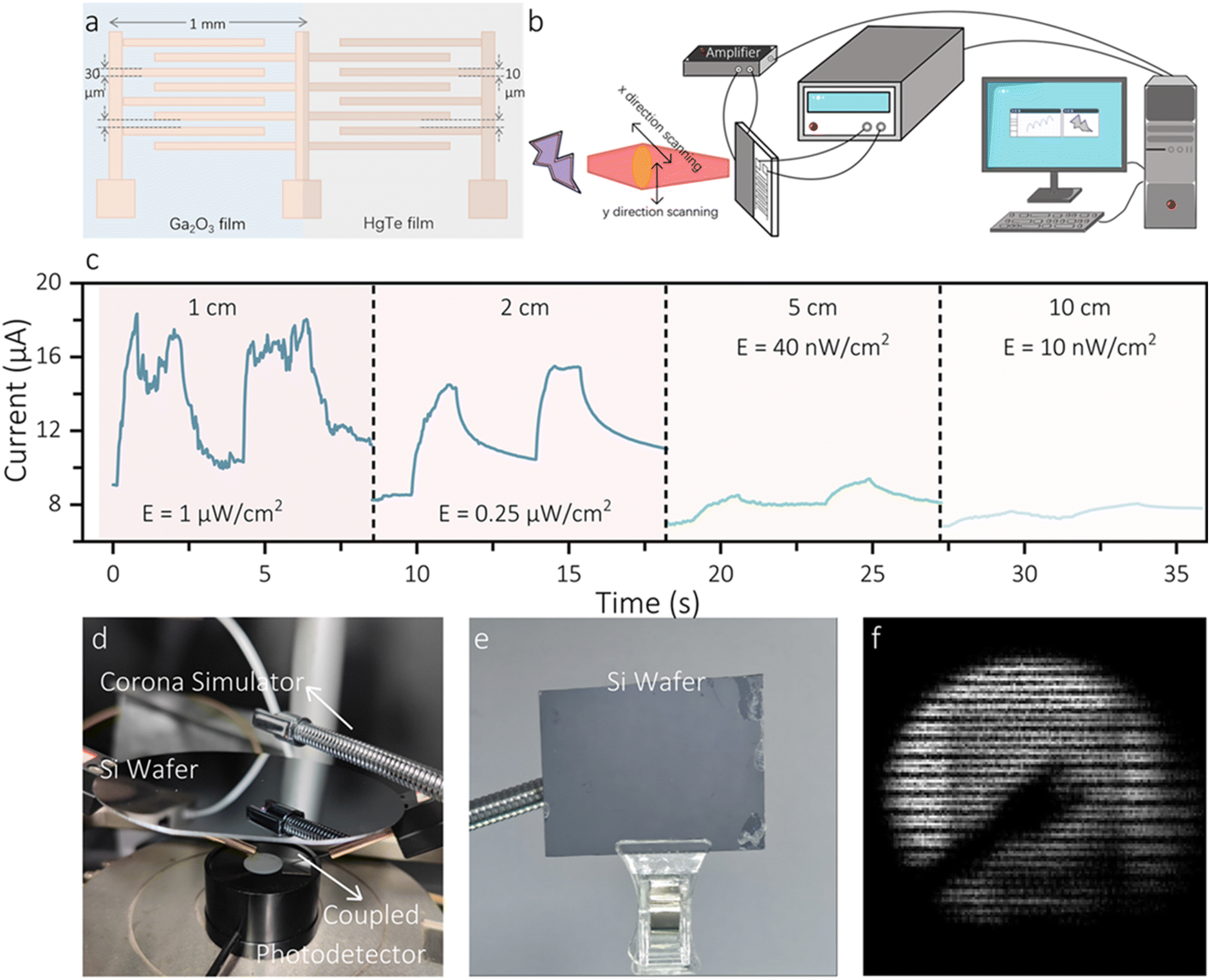 | ||
| Fig. 4 Dual-band coupled photodetector for corona detection. (a) Schematic of the coupled photoconductor; (b) schematic of the detection process; (c) corona discharge detection results at different distances; (d) corona detection by the SBPD under Si wafer; visible (e) and SWIR (f) images of the arc simulator. | ||
As the distance between the simulator and the SBPD rises, the quantity of photons drops, and at a distance of 10 cm, the number of photons is roughly 3 × 10⁷ photons per s.
In practice, considering that corona detection can be significantly influenced by environmental factors, particularly when electromagnetic signal propagation is blocked, as in Fig. 4d, an opaque silicon wafer is used to block the signal released by the corona simulator, and the device at this point no longer has any photoresponse to the high-voltage corona, as shown in Fig. S4,† implying that the UV detection capability is completely eliminated. Instead, the reflected light of the object from the external light (such as a tungsten lamp or sunlight) is projected onto the CQD device through the lens. The opaque silicon wafer in the visible image is found to be transparent in the SWIR region as shown in Fig. 4e and f. This is an effective solution to the problem of missed detection owing to barriers between the detector and the high voltage line, and it is anticipated to be one of the options for corona discharge detection in the future.
4. Conclusions
In this study, we coupled a HgTe CQD photoconductive device and an a-Ga2O3 SBPD to fabricate photodetectors with dual-band detection capability. At a light intensity of 5 μW cm−2, the constructed SBPD had an ultra-high responsivity of 1808 A W−1, and D* and EQE were up to 3.88 × 10¹⁴ and 8.8 × 10⁵%, respectively. The HgTe CQD photoconductor achieved a detectivity of 1.45 × 10¹⁰ and a response time of 720/292 μs. Furthermore, we used the dual-band coupled optoelectronic device in corona detection and demonstrated high-voltage corona detection.Data availability
Data will be made available on request.Author contributions
All authors commented on the manuscript. All authors have given approval to the final version of the manuscript. Q. Z. finished the photodetector fabrication and characterization as well as drafting the manuscript, and J. Y. assisted in the characterization of the photodetectors. Y. Y., L. L. and A. X. finished data analysis. K. Z. and X. X. finished the CQD synthesis. L. M. finished imaging experiment. W. L. and M. C. worked on conceptualization, study design and data analysis.Conflicts of interest
The authors declare no competing financial interests.Acknowledgements
This work is supported by Optoelectronic Measurement and Intelligent Perception Zhongguancun Open Lab LabSOMP-2024-01, National Natural Science Foundation of China (No. 62475012); State Key Laboratory of Materials for Integrated Circuits (No. SKLJC-K2024-07); Beijing National Laboratory for Condensed Matter Physics (No. 2023BNLCMPKF012); and Westlake Institute for Optoelectronics (No. 2024GD003).References
- D. Lee, S. Jeong, S. Moon, M. Yang, S. Kim, D. Kim, S. Lee, I. Lee, D. Jeon, J. Park, J. Kim and S. Baek, ACS Nano, 2024, 18(51), 34741–34749 CrossRef CAS PubMed.
- G. Ariyawansa, M. B. M. Rinzan, M. Alevli, M. Strassburg, N. Dietz, A. G. U. Perera, S. G. Matsik, A. Asghak, I. T. Ferguson, H. Luo, A. Bezinger and H. C. Liu, Appl. Phys. Lett., 2006, 89, 9 Search PubMed.
- J. He, X. S. Xing, X. B. Song, S. Y. Li, C. Zhang and W. Wang, Proceedings of the 3rd ICITEE, 2020, pp. 202–207 Search PubMed.
- W. Zheng, R. Lin, J. X. Ran, Z. J. Zhang, X. Ji and F. Huang, ACS Nano, 2018, 12, 425–431 CrossRef CAS PubMed.
- C. H. Zeng, W. K. Lin, Y. H. Sun, Q. Cui, X. Zhang, S. J. Li, B. S. Zhang and M. Kong, Optoelectronics Letters, 2019, 15, 170–173 CrossRef.
- Z. F. Zhang, C. N. Lin, X. Yang, J. H. Zang, K. Y. Li, Y. C. Lu, Y. Z. Li, L. Dong and C. X. Shan, J. Mater. Chem. C, 2022, 10, 6488–6496 RSC.
- M. R. Chen, S. H. Chang, T. C. Chen, C. H. Hsu, H. L. Kao and J. I. Chyi, Phys. Status Solidi A, 2010, 207, 224–228 CrossRef CAS.
- J. H. Kim, C. Y. Han, K. H. Lee, K. S. An, W. Song, J. Kim, M. S. Oh, Y. R. Do and H. Yang, Chem. Mater., 2015, 27, 197–204 CrossRef CAS.
- Y. Qin, L. H. Li, Z. Yu, F. Wu, D. Dong, W. Guo, Z. F. Zhang, J. H. Yuan, K. H. Xue, X. S. Miao and S. B. Long, Adv. Sci., 2021, 8, 2101106 CrossRef CAS PubMed.
- C. Xie, X. Lu, Y. Liang, H. Chen, L. Wang, C. Wu, W. H. Yang and L. B. Luo, J. Mater. Sci. Technol., 2021, 72, 189–196 CrossRef CAS.
- S. R. Zhou, Q. Q. Zheng, C. X. Yu, Z. H. Huang, L. R. Chen, H. Zhang, H. L. Li, Y. Q. Xiong, C. Y. Kong, L. J. Ye and W. J. Li, Mater, 2022, 16, 295 CrossRef PubMed.
- H. Yang, Y. Liu, X. G. Luo, Y. Li, D. S. Wuu, K. Y. He and Z. C. Feng, Superlattices Microstruct., 2019, 131, 21–29 CrossRef CAS.
- W. Y. Kong, G. A. Wu, K. Y. Wang, T. F. Zhang, Y. F. Zou, D. D. Wang and L. B. Luo, Adv. Mater., 2016, 28, 10725–10731 CrossRef CAS PubMed.
- A. Almalki, L. Madani, N. Sengouga, S. Alhassan, S. Alotaibi, A. Alhassni, A. Almunyif, J. S. Chauhan, M. Henini, H. V. A. Galeti, Y. G. Gobato, M. P. F. Godoy, M. B. Andrade, S. Souto, H. Zhou, B. Y. Wang, M. Xiao, Y. Qin and Y. H. Zhang, Mater. Today Electron., 2023, 4, 100042 CrossRef.
- T. He, C. Li, X. Zhang, Y. J. Ma, X. Cao, X. Y. Shi, C. Shi, J. S. Li, L. Song, C. H. Zeng, K. Zhang, X. P. Zhang and B. S. Zhang, Phys. Status Solidi A, 2020, 217, 1900861 CrossRef CAS.
- T. Chen, J. R. Zhang, X. D. Zhang, C. Chen, L. Zhang and Y. Hu, IEEE Sens. J., 2023, 23, 15504–15511 CAS.
- X. Zhao, X. Tang, T. P. Li and M. L. Chen, Infrared Phys. Technol., 2023, 133, 104788 CrossRef CAS.
- S. G. Kumar and K. K. Rao, Energy Environ. Sci., 2014, 7, 45–102 RSC.
- X. M. Xue, M. L. Chen, Y. N. Luo, T. L. Qin, X. Tang and Q. Hao, Light: Sci. Appl., 2023, 12, 2 CrossRef CAS PubMed.
- Y. Luo, S. Zhang, X. Tang and M. L. Chen, J. Mater. Chem. C, 2022, 10, 8218–8225 RSC.
- X. M. Xue, Q. Hao and M. L. Chen, Light: Sci. Appl., 2024, 13, 89 CrossRef CAS PubMed.
- Y. Y. Qiu, N. Q. Yan, H. F. Yao and M. L. Chen, Infrared Phys. Technol., 2023, 135, 104980 CrossRef CAS.
- S. Zhang, C. Bi, Y. M. Tan, Y. N. Luo, Y. F. Liu, J. Cao, M. L. Chen, Q. Hao and X. Tang, ACS Nano, 2022, 16, 18822–18829 CrossRef CAS PubMed.
- X. D. Li, F. Y. Xu, X. Wang, J. S. Luo, K. Ding, L. Y. Ye, H. L. Li, Y. Q. Xiong, P. Yu, C. Y. Kong, L. J. Ye, H. Zhang and W. J. Li, Phys. Status Solidi RRL, 2024, 18, 2200512 CrossRef CAS.
- Z. K. Liu, P. Wang, R. Dong, W. Gong, J. J. Li, D. C. Dai, H. Yan and Y. Z. Zhang, Coatings, 2022, 12, 1033 CrossRef CAS.
- J. Bae, D. W. Jeon, J. H. Park and J. Kim, J. Vac. Sci. Technol., A, 2021, 39, 033410 CrossRef CAS.
- H. T. Zhou, L. J. Cong, J. G. Ma, B. S. Li, M. Z. Chen, H. Y. Xu and Y. C. Liu, J. Mater. Chem. C, 2019, 7, 13149–13155 RSC.
- Z. H. Huang, S. R. Zhou, L. R. Chen, Q. Q. Zheng, H. L. Li, Y. Q. Xiong, L. J. Ye, C. Y. Kong, S. Q. Fan, H. Zhang and W. J. Li, Crystals, 2022, 12, 1427 CrossRef CAS.
- S. R. Zhou, H. Zhang, X. Peng, H. W. Liu, H. L. Li, Y. Q. Xiong, W. J. Li, P. A. Yang, L. J. Ye and C. Y. Kong, Adv. Photonics Res., 2022, 3, 2202192 Search PubMed.
- L. Wang, J. S. Jie, Z. B. Shao, Q. Zhang, X. H. Zhang, Y. M. Wang, S. Zheng and S. Lee, Adv. Funct. Mater., 2015, 25, 2910–2919 CrossRef CAS.
- Y. Qin, L. H. Li, X. L. Zhao, G. S. Tompa, H. Dong, G. Z. Jian, Q. M. He, P. J. Tan, X. H. Hou, Z. F. Zhang, S. J. Yu, H. D. Sun, G. W. Xu, X. S. Miao, K. H. Xue, S. B. Long and M. Liu, ACS Photonics, 2020, 7, 812–820 CrossRef CAS.
- J. Wang, Y. Q. Xiong, L. J. Ye, W. J. Li, G. P. Qin, H. B. Ruan, H. Zhang, L. Fang, C. Y. Kong and H. L. Li, Opt. Mater., 2021, 112, 110808 CrossRef CAS.
- C. T. Wei, J. P. Xu, S. B. Shi, R. Cao, J. Chen, H. Dong, X. S. Zhang, S. G. Yin and L. Li, J. Mater. Chem. C, 2019, 7, 9369–9379 RSC.
- Q. Q. Zheng, L. R. Chen, X. D. Li, K. Ding, D. Pang, H. L. Li, Y. Q. Xiong, H. B. Ruan, L. Fang, W. J. Li, L. J. Ye, H. Zhang and C. Y. Kong, Sci. China: Technol. Sci., 2023, 66, 2707–2715 CrossRef CAS.
- K. H. Li, X. K. Yang, F. F. Yang, J. G. He, G. Z. Zhang, S. L. Jiang, C. Chen and J. Tang, Mater. Today Electron., 2022, 2, 100011 CrossRef.
- X. C. Liang, C. Hou, Z. H. Wu, Z. T. Wu and G. A. Tai, Nanotechnology, 2023, 34, 205701 CrossRef CAS PubMed.
- Z. H. Wu, C. Shifan, Z. T. Wu, Y. Liu, W. Shao, X. C. Liang, C. Hou and G. A. Tai, Nano Res., 2024, 17, 3053–3060 CrossRef CAS.
- Y. Liu, G. A. Tai, C. Hou, Z. T. Wu and X. C. Liang, ACS Appl. Mater. Interfaces, 2023, 15, 14566–14574 CAS.
- G. A. Tai, B. Liu, C. Hou, Z. T. Wu and X. C. Liang, Nanotechnology, 2021, 32, 505606 CrossRef CAS PubMed.
- S. Oh, C. K. Kim and J. Kim, ACS Photonics, 2017, 5, 1123–1128 CrossRef.
- L. Chen, B. Y. Wang, J. Q. Dong, F. L. Gao, H. W. Zheng, M. He and X. F. Wang, Nano Energy, 2020, 78, 105260 CrossRef CAS.
- Y. L. Yu, Y. Hu, J. H. Yang and Z. M. Wei, Mater. Today Electron., 2022, 2, 100013 CrossRef.
- Y. H. Wang, S. Y. Li, J. Cao, Y. C. Jiang, Y. Zhang, W. H. Tang and Z. P. Wu, Mater. Des., 2022, 221, 110917 CrossRef CAS.
- X. M. Xue, Y. N. Luo, Q. Hao, J. Cao, X. Tang, Y. F. Liu and M. L. Chen, ACS Photonics, 2023, 10, 4290–4298 CrossRef CAS.
- M. M. Yaacob, M. A. Alsaedi, J. R. Rashed, A. M. Dakhil and S. F. Atyah, Photonic Sens., 2014, 4, 325–337 CrossRef.
- H. W. Liu, S. R. Zhou, H. Zhang, L. J. Ye, Y. Q. Xiong, P. Yu, W. J. Li, X. Yang, H. L. Li and K. C. Yang, J. Phys. D: Appl. Phys., 2022, 55, 305104 CrossRef CAS.
- Y. Q. Yu, L. B. Luo, M. Z. Wang, B. Wang, L. H. Zeng, C. Y. Wu, J. S. Jie, J. W. Liu, L. Wang and S. H. Yu, Nano Res., 2015, 8, 1098–1107 CrossRef CAS.
- M. Rabia, A. M. Elsayed and M. A. Alnuwaiser, Micromachines, 2023, 14, 1573 CrossRef PubMed.
- Y. Q. Yu, L. B. Luo, M. Z. Wang, B. Wang, L. H. Zeng, C. Y. Wu, J. S. Jie, J. W. Liu, L. Wang and S. H. Yu, Nano Res., 2015, 8, 1098–1107 CrossRef CAS.
Footnote |
| † Electronic supplementary information (ESI) available. See DOI: https://doi.org/10.1039/d4na00978a |
| This journal is © The Royal Society of Chemistry 2025 |