
 Open Access Article
 This Open Access Article is licensed under a Creative Commons Attribution-Non Commercial 3.0 Unported Licence
Performance enhancement of InSnZnO thin-film transistors by modifying the dielectric–semiconductor interface with colloidal quantum dots†
Sijie
Chen
a,
Haoran
Chen
b,
Chenghui
Xia
 *b and
Zhenhua
Sun
*a
*b and
Zhenhua
Sun
*a
aKey Laboratory of Optoelectronic Devices and Systems of Ministry of Education and Guangdong Province, State Key Laboratory of Radio Frequency Heterogeneous Integration, College of Physics and Optoelectronic Engineering, Shenzhen University, Shenzhen 518060, China. E-mail: szh@szu.edu.cn
bSchool of Materials Science and Engineering, Ocean University of China, Qingdao, Shandong 266404, China. E-mail: c.xia@ouc.edu.cn
First published on 27th December 2024
Abstract
Thin film transistors (TFTs) with InSnZnO (ITZO) and Al2O3 as the semiconductor and dielectric layers, respectively, were investigated, aiming to elevate the device performance. Chemically synthesized CuInS2/ZnS core/shell colloidal quantum dots (QDs) were used to passivate the semiconductor/dielectric interface. Compared with the pristine device, the device with the integrated QDs demonstrates remarkably improved electrical performance, including a higher electron mobility and a lower leakage current. Moreover, the integration of QDs largely mitigates hysteresis in the bidirectional transfer characteristics of the device. Improved negative bias stress stability is also observed in the device with QDs. The performance enhancement is ascribed to the reduction of the trap states induced by the defects in Al2O3, and the screening of electrical dipoles at the Al2O3/ITZO interface. This work proposes a new strategy to passivate the semiconductor/dielectric interface, which not only improves TFT performance, but also holds potential for optoelectronic applications.
Introduction
Thin film transistors (TFTs) are fundamental components in a wide array of electronic applications, including display technologies, sensors, and flexible electronics. The continuous advancement of TFT technology necessitates the exploration of novel materials and structures to enhance device performance and reliability. Indium tin zinc oxide (ITZO) offers several advantages that make it a compelling choice of semiconductor for TFTs. Firstly, ITZO TFTs exhibit high carrier mobility, facilitated by the direct spatial overlap between the 5s orbitals of Sn and In, which enhances the movement of electron carriers and improves device performance.1 Secondly, ITZO possesses a wide bandgap, enabling high transparency within the visible light range, which makes it suitable as a transparent semiconductor layer in displays and other optoelectronic devices.2–4 Furthermore, ITZO TFTs can be seamlessly integrated into the commercially successful IGZO TFT production lines without incurring additional costs, thus facilitating commercialization.2 However, achieving low-voltage operation in portable and wearable electronic devices, which is crucial due to limited battery capacity, remains a challenge for oxide semiconductor TFTs. The key strategy for maintaining good device performance, such as high field-effect mobility and stability, while reducing operating voltage, is the incorporation of high-k gate dielectrics.5–7 High-k dielectric materials, including Al2O3,8,9 Ta2O5,10 HfO2,11, and ZrO2,12, and their stacking13 provide high capacitance, allowing TFTs to operate at lower voltages and thereby reducing power consumption in logic circuits.14,15 Moreover, high-k dielectrics offer a larger physical thickness at the same effective oxide thickness (EOT) compared to traditional SiO2, effectively suppressing tunnelling effects and reducing leakage current.16,17 The high-k dielectrics are normally grown at relative low temperatures, inducing defects and doping.18 For example, an Al2O3 dielectric layer grown by low temperature atomic layer deposition (ALD) usually has oxygen vacancies (VO) and high levels of impurities, such as H, C and OH− residues.19–22The overall performance and lifespan of TFTs are also influenced by their stability and reliability. Factors such as device structure, dielectric materials, and manufacturing processes play critical roles in the electrical performance and stability of oxide semiconductor TFTs. Reliability tests for evaluating TFTs include threshold voltage shifts caused by hysteresis effects, observed in both organic thin film transistors (OTFTs) and metal oxide semiconductor field effect transistors (MOSFETs). Maintaining good bias stability under positive bias stress (PBS) and negative bias stress (NBS) is essential for oxide semiconductor TFTs. Bias instability and hysteresis effects are generally attributed to charge trapping at the semiconductor/dielectric interface or the generation of defects/traps in the semiconductor layer.23,24 Oxygen-related defects, such as oxygen vacancies and weakly bonded oxygen, are closely linked to these instabilities.24,25 Additionally, water and oxygen molecules absorbed from the air can create traps in the channel layer.26 Methods such as thermal annealing,2 doping,27,28 and dual channel layers29–31 are commonly used to reduce defects and improve stability issues.
To address stability issues caused by interface defects, we propose using quantum dots to passivate the interface. Here, we report ITZO TFTs based on an Al2O3 dielectric layer with a CuInS2/ZnS core/shell quantum dots (CIS/ZnS QDs) passivation layer. The low-cost spin-coating method was used to prepare quantum dot films in a top-gate configuration TFT. The results show that compared to pure ITZO TFTs, those passivated with quantum dots exhibit higher mobility, less electrical hysteresis, and improved bias stability. These performance enhancements reveal that the colloidal QDs can effectively improve the interface between ITZO and Al2O3. In light of the diverse range of QD types, this approach holds significant potential for advancing low-power, high-performance portable and wearable electronic and optoelectronic devices.
Experimental
CIS/ZnS QD synthesis and characterization
The CIS/ZnS QDs used in the study were prepared by topotactic Cu+ to In3+ cation exchange in template Cu2−xS nanocrystals followed by heteroepitaxial overgrowth of a ZnS shell according to the previously reported procedures.32 The detailed synthesis process is described in the ESI.† As can be seen in Fig. 1a, the product QDs are rather monodisperse and display a pyramidal shape with an average size of ∼11.1 nm. High-resolution transmission electron microscopy (TEM) images show that the QDs exhibit clear lattice fringes. The corresponding fast Fourier transform analysis of a single nanocrystal confirms that the particle has a hexagonal wurtzite crystal structure, which is highly consistent with the results of the selected area electron diffraction patterns shown in Fig. 1c and d. The diffraction pattern slightly shifts to higher angles which is likely due to a strong lattice stress caused by an ultra-thick ZnS shell (∼ten monolayers of ZnS).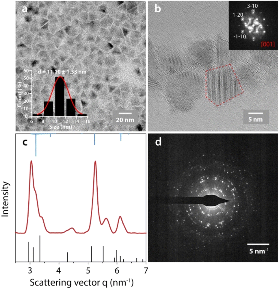 | ||
| Fig. 1 Structure characterization of the product CIS/ZnS core/shell nanocrystals. (a) Conventional TEM image of CIS/ZnS quantum dots. (b) High-resolution TEM image and the corresponding Fourier transform pattern of CIS/ZnS QDs. The Fourier transform pattern is indexed to the [001] projection of hexagonal wurtzite CuInS2. (c) One dimensional electron diffraction pattern obtained by the azimuthal integration of the two-dimensional electron diffraction pattern shown on the right side. The black line represents the diffraction peak of hexagonal wurtzite CIS (PDF No. 97-016-3489) and the blue line represents the diffraction peak of hexagonal wurtzite ZnS (PDF No. 97-004-2819). (d) Selected area electron diffraction pattern of the product CIS/ZnS nanocrystals. | ||
Device fabrication and characterization
The ITZO TFTs studied here have a top-gate–bottom contact structure, as shown in Fig. 2a. Specifically, on a clean glass substrate, gold source and drain electrodes were deposited by thermal evaporation through a shadow mask, defining a source–drain channel with a width/length ratio of 2/0.4 mm. Then a 12 nm-thick ITZO thin film was deposited via radio-frequency (RF) magnetron sputtering (RF power = 60 W, pressure = 0.4 Pa, and O2![[thin space (1/6-em)]](https://www.rsc.org/images/entities/char_2009.gif) :Ar = 5:12) using ceramic targets (In2O3:SnO2:ZnO = 1:2:1 at%). Next, the ITZO film was annealed at 350 °C for 2 min using a rapid thermal process (RTP) oven. After that, the colloidal QD solution was spin-coated atop at a spinning speed of 3000 rpm for 30 seconds, forming a QD film with a thickness of about 12 nm. Then a 22 nm-thick Al2O3 film was grown at 150 °C by the atomic layer deposition (ALD) method, using trimethylaluminum (TMA) and H2O as precursors. Finally, an Al film was thermally evaporated on the Al2O3 film as the gate electrode. For comparison, a device without the QDs was also fabricated using the same process but with the QD film deposition step omitted. Hereafter, the ITZO TFT with QDs is referred to as the w-QD device, and the one without QDs is referred to as the w/o-QD device. The SEM images of the Al2O3 film and the QD film surfaces were characterized and are shown in Fig. 2b and c, respectively. The Al2O3 film demonstrates a flat, smooth and uniform surface. In contrast, the surface of the QD film is very rough. There are stripe-like structures in the QD film, with lengths of hundreds of nanometers and widths of tens of nanometers, which are attributed to the aggregation of quantum dots. They exhibit the different dielectric/semiconductor interfaces of the w-QD and w/o-QD devices.
:Ar = 5:12) using ceramic targets (In2O3:SnO2:ZnO = 1:2:1 at%). Next, the ITZO film was annealed at 350 °C for 2 min using a rapid thermal process (RTP) oven. After that, the colloidal QD solution was spin-coated atop at a spinning speed of 3000 rpm for 30 seconds, forming a QD film with a thickness of about 12 nm. Then a 22 nm-thick Al2O3 film was grown at 150 °C by the atomic layer deposition (ALD) method, using trimethylaluminum (TMA) and H2O as precursors. Finally, an Al film was thermally evaporated on the Al2O3 film as the gate electrode. For comparison, a device without the QDs was also fabricated using the same process but with the QD film deposition step omitted. Hereafter, the ITZO TFT with QDs is referred to as the w-QD device, and the one without QDs is referred to as the w/o-QD device. The SEM images of the Al2O3 film and the QD film surfaces were characterized and are shown in Fig. 2b and c, respectively. The Al2O3 film demonstrates a flat, smooth and uniform surface. In contrast, the surface of the QD film is very rough. There are stripe-like structures in the QD film, with lengths of hundreds of nanometers and widths of tens of nanometers, which are attributed to the aggregation of quantum dots. They exhibit the different dielectric/semiconductor interfaces of the w-QD and w/o-QD devices.
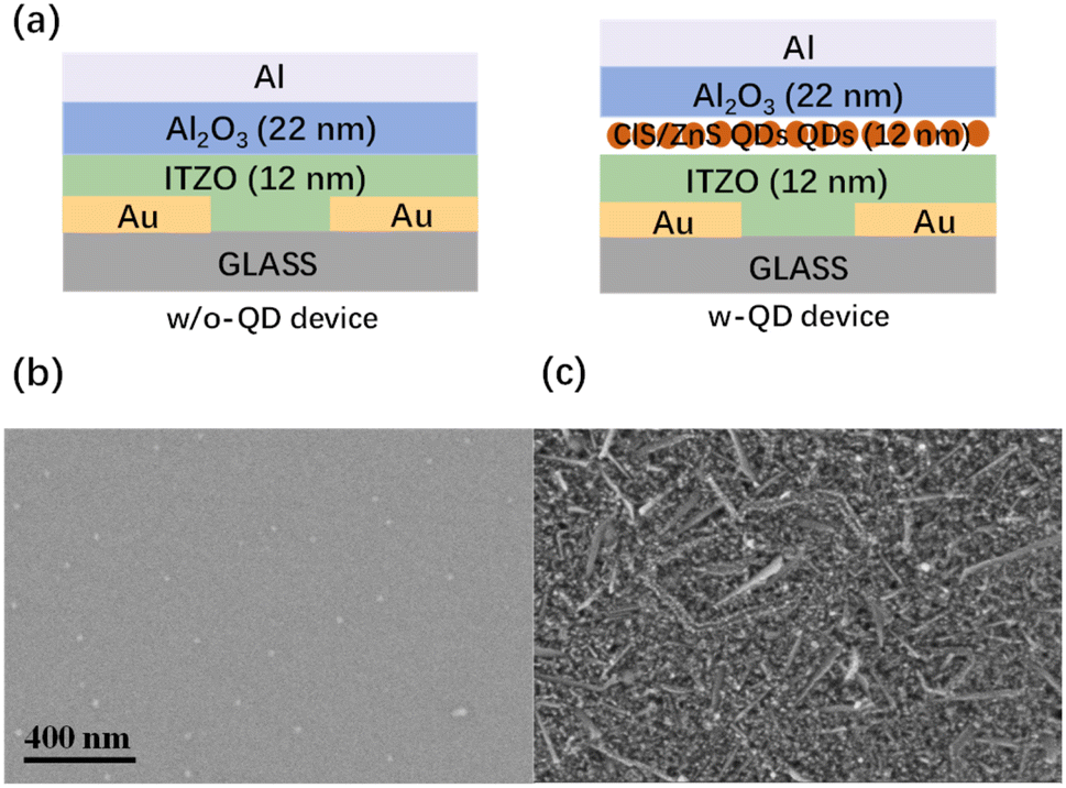 | ||
| Fig. 2 (a) Schematic of the device structures. SEM images of Al2O3 (b) and QDs films (c). | ||
The electrical characterization of the devices was performed using a combination of a probe station and a Keysight B2902B instrument in an inert gas glove box (nitrogen purity >99.99%). The capacitance measurement was conducted using a Keysight E4990A impedance analyzer.
Results and discussion
Electrical characterization was first conducted to investigate the effect of QDs on the device performance. Fig. 3a shows the representative transfer characteristics of the two types of devices under linear (VDS = 0.5 V) and saturation (VDS = 5 V) conditions. The ITZO TFTs exhibit a typical n-channel conduction behaviour. The w-QD device demonstrates a higher current than the w/o-QD device. Fig. 3b shows the leakage current (IGS) of the two different devices. With the integration of the QDs, the leakage current gets apparently suppressed. Fig. 3c shows the output characteristics of the two devices. They verify the good ohmic contact between the electrode and ITZO, as well as the improvement of the channel current with the integration of the QDs, which is consistent with the transfer characteristics. Eight w-QD devices and six w/o-QD devices were fabricated and characterized. The results corroborate the overall improvement in the device with the integration of the QDs. Two capacitors with different structures, Al/Al2O3/Al and Al/Al2O3-QDs/Al, were fabricated. Their capacitance–voltage characteristics were measured, and their dielectric constants were calculated, as shown in Fig. S1.† The dielectric constant of the Al2O3 and Al2O3-QDs hybrid films were ascertained to be 5.59 and 7.37, respectively. On this basis, the electron mobilities of these devices are extracted and shown in Fig. 3d. It can be seen that compared to the w/o-QD device, the w-QD device exhibits higher linear and saturation mobilities. Please note that the mobilities observed in our devices are lower than those reported for some ITZO TFTs,2,18,27,31,33–37 which may be due to the suboptimal quality of the ITZO films. However, given that all devices were fabricated using the same procedure, the comparison between the devices with and without QD passivation remains valid and meaningful. | ||
| Fig. 3 Comparisons of the electrical characteristics of the w-QD and w/o-QD devices. (a) transfer characteristics; (b) leakage currents; (c) output characteristics; (d) electron mobilities. The statistical mobility data are obtained from eight w-QD and six w/o-QD devices. | ||
To realize a reliable logic function, a TFT is supposed to work stably under different bias conditions including sweep direction and duration. To investigate the influence of QDs on the stability of ITZO TFTs, we conducted two tests. First, we performed repeated tests on both devices across different gate voltage ranges. The gate-source voltage (VGS) was set to undergo bidirectional sweeps from negative to positive and back to negative. The sweep ranges included ten sets of tests, spanning from −1 V to 1 V, −2 V to 2 V, −3 V to 3 V, and so on, up to −10 V to 10 V. For the linear state, the VDS was set to 0.5 V, and for the saturation state, VDS was set to 10 V. The resulting transfer characteristic curves of the w/o-QD and w-QD devices are shown in Fig. 4a and b. Regarding threshold voltage stability, the w/o-QD device in the saturation state exhibits a gradual rightward shift in the threshold voltage as the VGS sweep range increases. In contrast, the w-QD device maintains a stable threshold voltage, indicating that QD passivation can effectively enhance threshold voltage stability. The memory window, an important indicator of the hysteresis effect, was quantitatively evaluated by selecting the difference between the two VGS values corresponding to IDS = 1.0 × 10⁻⁸ A. The memory windows obtained are plotted along with the sweeping range in Fig. 4c and d. The results indicate that for the w/o-QD device, regardless of whether it is in the linear or saturation state, when the VGS sweep range exceeds −5 V to 5 V, the memory window increases linearly, reaching 4.7 V (linear) and 2.0 V (saturation) at the maximum VGS sweep range (−10 V to 10 V). Conversely, for the w-QD device, under all test conditions, the maximum memory window is only about 0.1 V.
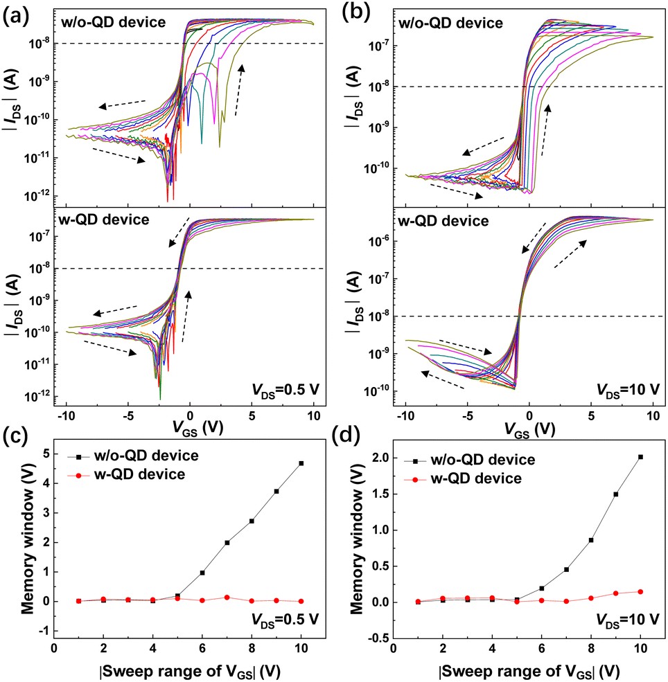 | ||
| Fig. 4 Linear (a) and saturation (b) transfer characteristics of the w/o-QD and w-QD devices. The dashed lines indicate the level of IDS at which the memory window value is extracted; memory windows extracted from the linear (c) and saturation (d) transfer curves. | ||
The counterclockwise hysteresis window observed suggests the presence of deep traps resembling receptors near the Al2O3/ITZO interface. As the scanning process starts, trapped electrons accumulate at the Al2O3/ITZO interface and screen the external electric field, causing a positive shift in the threshold voltage. As the scanning process reversed, the accumulated electrons started to release, inducing a negative shift in the threshold voltage.38,39 Together, they generate a counterclockwise hysteresis. Further studies indicate that electrical dipoles in the channel/dielectric layer also contribute to the hysteresis observed in TFTs.40 Thus, it is inferred that the Al2O3/QDs/ITZO interface can reduce trap density, likely due to a reduction in carbon-related impurities.2,41 Meanwhile, the existence of the QD layer can screen the electrical dipoles at the Al2O3/ITZO interface, significantly mitigating the hysteresis effect during bidirectional scanning.
Secondly, negative bias stress (NBS) and positive bias stress (PBS) tests were performed on both w/o-QD and w-QD devices. During these tests, the transfer characteristics of the devices were measured after applying a gate bias stress of −10 V for NBS and 10 V for PBS, each applied for varying durations. Fig. 5a and b display the resulting transfer characteristics of the w/o-QD (top) and w-QD (bottom) devices following NBS and PBS operations, respectively. Despite the current reduction phenomenon, both PBS tests of the w/o-QD device and w-QD device demonstrate good electrical performance, which can be ascribed to that the ionic bonding properties of Al2O3 that lead to the reduction of electronic traps.42 Nevertheless, under NBS stability testing, it can be clearly observed that the current of the w/o-QD device gradually decreases with the accumulation of bias time. While the w-QD device can resist the negative bias effect after introducing QDs, maintaining the stability of the IDS current, which proves that the introduction of QDs can significantly improve the stability of the device. It has been shown that NBS elevates the Fermi level in ITZO, leading to a leftward shift of the threshold voltage in the transfer characteristics.2 However, our devices exhibit a different response. As shown in Fig. 5a, the NBS induces an increase in the subthreshold slope, rather than a shift in the threshold voltage. Since the subthreshold slope is positively related to the density of trapped charge carriers at the dielectric/semiconductor interface,43,44 we speculate that a large number of traps are present at the Al2O3/ITZO interface, rather than in the ITZO bulk. The introduction of quantum dots at this interface helps to mitigate the effect of these interface traps. This conclusion is further supported by the elimination of hysteresis in the transfer curves of the QD-passivated devices (Fig. 4) and is likely responsible for the improvement in mobility observed in Fig. 3.
 | ||
| Fig. 5 Transfer characteristics of TFTs after NBS (a) and PBS (b). The transfer curves were recorded after applying gate bias stresses denoted in the figures. | ||
Conclusions
In this study, two types of TFTs using ITZO as the semiconductor and Al2O3 as the dielectric layer are fabricated and systemically investigated: one with CuInS2/ZnS core/shell QDs integrated into the Al2O3/ITZO interface and one without. Through testing, it was found that the QD integration can significantly increase the on-current, decrease the leakage current, and finally improve electron mobility. Furthermore, compared with the counterpart, TFTs with QDs show transfer characteristics with less hysteresis and improved NBS stability. The overall performance enhancement can be ascribed to the passivation effect of the QDs at the Al2O3/ITZO interface, which can eliminate the trap states in the Al2O3 and screen the electric dipoles.Data availability
The datasets used and/or analysed during the current study are available from the corresponding author on reasonable request.Author contributions
Sijie Chen: investigation, methodology, data curation, writing – original draft. Haoran Chen: investigation, methodology, data curation. Chenghui Xia: conceptualization, methodology, supervision, funding acquisition, writing – review and editing. Zhenhua Sun: conceptualization, data curation, methodology, supervision, funding acquisition, writing – review and editing.Conflicts of interest
There are no conflicts to declare.Acknowledgements
The authors acknowledge the financial support from the Natural Science Foundation of Shenzhen (grant no. JCYJ20210324095400002 and JCYJ20240813142459010), the Shenzhen Science and Technology Program (Shenzhen Key Laboratory of Ultrafast Laser Micro/Nano Manufacturing ZDSYS20220606100405013), the Department of Science and Technology of Guangdong (grant no. 2020B010169003), the TaiShan Scholars of Shandong China (grant no. tsqn202306113), and the Excellent Youth Science Fund Project Shandong China (grant no. 2024HWYQ-037).References
- J.-Y. Noh, H. Kim, H.-H. Nahm, Y.-S. Kim, D. Hwan Kim, B.-D. Ahn, J.-H. Lim, G. Hee Kim, J.-H. Lee and J. Song, J. Appl. Phys., 2013, 113, 183706 CrossRef.
- Y.-S. Shiah, K. Sim, Y. Shi, K. Abe, S. Ueda, M. Sasase, J. Kim and H. Hosono, Nat. Electron., 2021, 4, 800–807 CrossRef CAS.
- J. Shi, J. Zhang, L. Yang, M. Qu, D. C. Qi and K. H. Zhang, Adv. Mater., 2021, 33, 2006230 CrossRef CAS PubMed.
- E. Fortunato, P. Barquinha and R. Martins, Adv. Mater., 2012, 24, 2945–2986 CrossRef CAS PubMed.
- A. Liu, H. Zhu, H. Sun, Y. Xu and Y. Y. Noh, Adv. Mater., 2018, 30, 1706364 CrossRef PubMed.
- L. Zhu, G. He, W. Li, B. Yang, E. Fortunato and R. Martins, Adv. Electron. Mater., 2018, 4, 1800100 CrossRef.
- Y. Zhang, G. He, W. Wang, B. Yang, C. Zhang and Y. Xia, J. Mater. Sci. Technol., 2020, 50, 1–12 CrossRef CAS.
- P. Ma, L. Du, Y. Wang, R. Jiang, Q. Xin, Y. Li and A. Song, Appl. Phys. Lett., 2018, 112, 023501 CrossRef.
- W. Cai, H. Li and Z. Zang, IEEE Electron Device Lett., 2021, 42, 525–528 CAS.
- C. Brox-Nilsen, J. Jin, Y. Luo, P. Bao and A. M. Song, IEEE Trans. Electron Devices, 2013, 60, 3424–3429 CAS.
- P. Ma, J. Sun, G. Liang, Y. Li, Q. Xin, Y. Li and A. Song, Appl. Phys. Lett., 2018, 113, 063501 CrossRef.
- J. Zhang, M. Jia, M. G. Sales, Y. Zhao, G. Lin, P. Cui, C. Santiwipharat, C. Ni, S. McDonnell and Y. Zeng, ACS Appl. Electron. Mater., 2021, 3, 5483–5495 CrossRef CAS.
- M. Li, Q. Zhuang, S. Lu, Z. Zang and W. Cai, Appl. Phys. Lett., 2023, 122, 162104 CrossRef CAS.
- J. Ko, J. Kim, S. Y. Park, E. Lee, K. Kim, K. H. Lim and Y. S. Kim, J. Mater. Chem. C, 2014, 2, 1050–1056 RSC.
- J. Zhang, Y. Liu, L. Guo, N. Liu, H. Xiao, C. Chen and G. Wu, J. Mater. Sci. Technol., 2015, 31, 171–174 CrossRef CAS.
- X. Zhu, J. Zhu, A. Li, Z. Liu and N. Ming, J. Mater. Sci. Technol., 2009, 25, 289–313 CAS.
- G. He and L. Zhang, J. Mater. Sci. Technol., 2007, 23, 433–448 CAS.
- F. Chen, M. Zhang, Y. Wan, X. Xu, M. Wong and H.-S. Kwok, J. Semicond., 2023, 44, 091602 CrossRef CAS.
- J. Raja, C. P. T. Nguyen, C. Lee, N. Balaji, S. Chatterjee, K. Jang, H. Kim and J. Yi, IEEE Electron Device Lett., 2016, 37, 1272–1275 CAS.
- S. K. Kim, S. W. Lee, C. S. Hwang, Y. S. Min, J. Y. Won and J. Jeong, J. Electrochem. Soc., 2006, 153, F69–F76 CrossRef CAS.
- M. D. Groner, F. H. Fabreguette, J. W. Elam and S. M. George, Chem. Mater., 2004, 16, 639–645 CrossRef CAS.
- A. C. Dillon, A. W. Ott, J. D. Way and S. M. George, Surf. Sci., 1995, 322, 230–242 CrossRef CAS.
- D. Knipp, R. A. Street, A. Völkel and J. Ho, J. Appl. Phys., 2003, 93, 347–355 CrossRef CAS.
- K. Ide, K. Nomura, H. Hosono and T. Kamiya, Phys. Status Solidi A, 2019, 216, 1800372 CrossRef.
- Y. J. Chen, Y. H. Tai and C. Y. Chang, IEEE Trans. Electron Devices, 2016, 63, 1565–1571 CAS.
- W. Zhong, L. Y. Kang, S. B. Deng, L. Lu, R. H. Yao, L. F. Lan, H. S. Kwok and R. S. Chen, IEEE Trans. Electron Devices, 2021, 68, 4956–4961 CAS.
- H. Zhang, L. Liang, X. Wang, Z. Wu and H. Cao, IEEE Trans. Electron Devices, 2022, 69, 152–155 CAS.
- W. Cai, M. Li, H. Li, Q. Qian and Z. Zang, Appl. Phys. Lett., 2022, 121, 062108 CrossRef CAS.
- J. Jin, X. Y. Lin, J. W. Zhang, J. H. Lee, Z. Y. Xiao, S. Lee and J. Kim, Adv. Electron. Mater., 2023, 9, 2201117 CrossRef CAS.
- Z. Xiao, J. Jin, J. Lee, G. Choi, X. Y. Lin, J. W. Zhang and J. Kim, Phys. Status Solidi A, 2024, 221, 2300544 CrossRef CAS.
- L. Liang, H. Zhang, T. Li, W. Li, J. Gao, H. Zhang, M. Guo, S. Gao, Z. He, F. Liu, C. Ning, H. Cao, G. Yuan and C. Liu, Adv. Sci., 2023, 10, 2300373 CrossRef CAS PubMed.
- C. Xia, P. Tamarat, L. Hou, S. Busatto, J. D. Meeldijk, C. de Mello Donega and B. Lounis, ACS Nano, 2021, 15, 17573–17581 CrossRef CAS PubMed.
- W. Zhong, L. Kang, S. Deng, L. Lu, R. Yao, L. Lan, H. S. Kwok and R. Chen, IEEE Trans. Electron Devices, 2021, 68, 4956–4961 CAS.
- W. Zhong, R. Yao, Y. Liu, L. Lan and R. Chen, IEEE Trans. Electron Devices, 2020, 67, 3157–3162 CAS.
- X. Sun, J.-H. Han, Z. Xiao, S. Chen, T. Jin, T. Noh, S. Park, J. Kim, J. Jin and Y. Kim, ACS Appl. Electron. Mater., 2024, 6, 2442–2448 CrossRef CAS.
- Z. Xiao, J. Jin, J. Lee, G. Choi, X. Lin, J. Zhang and J. Kim, Phys. Status Solidi A, 2024, 221, 2300544 CrossRef CAS.
- J. Jin, X. Y. Lin, J. W. Zhang, J. H. Lee, Z. Y. Xiao, S. Lee and J. Kim, Adv. Electron. Mater., 2023, 9, 2201117 CrossRef CAS.
- N. Kaushik, D. M. A. Mackenzie, K. Thakar, N. Goyal, B. Mukherjee, P. Boggild, D. H. Petersen and S. Lodha, npj 2D Mater. Appl., 2017, 1, 34 CrossRef.
- S. William, M. F. Mabrook and D. M. Taylor, Appl. Phys. Lett., 2009, 95, 093309 CrossRef.
- Z. Ye, Y. Yuan, H. Xu, Y. Liu, J. Luo and M. Wong, IEEE Trans. Electron Devices, 2017, 64, 438–446 CAS.
- X. Chen, R. K. Wu, J. X. Wan, H. W. Wu, H. Wu and C. Liu, Vacuum, 2023, 215, 112315 CrossRef CAS.
- J. Lee, J. Jin, S. Maeng, G. Choi, H. Kim and J. Kim, ACS Appl. Electron. Mater., 2022, 4, 1800–1806 CrossRef CAS.
- A. Rolland, J. Richard, J. P. Kleider and D. Mencaraglia, J. Electrochem. Soc., 1993, 140, 3679 CrossRef CAS.
- J. Li, W. Tang, Q. Wang, W. Sun, Q. Zhang, X. Guo, X. Wang and F. Yan, Mater. Sci. Eng., R, 2018, 127, 1–36 CrossRef.
Footnote |
| † Electronic supplementary information (ESI) available. See DOI: https://doi.org/10.1039/d4na00967c |
| This journal is © The Royal Society of Chemistry 2025 |