
 Open Access Article
 This Open Access Article is licensed under a Creative Commons Attribution-Non Commercial 3.0 Unported Licence
A triradical-containing trinuclear Pd(II) complex: spin-polarized electronic transmission, analog resistive switching and neuromorphic advancements†
Prasenjit
Sarkar‡
 a,
Litty Thomas
Manamel‡
b,
Puranjay
Saha‡
b,
Chinmay
Jana
a,
Amrit
Sarmah
cd,
Kannan Udaya
Mohanan
e,
Bikas C.
Das
*b and
Chandan
Mukherjee
*a
a,
Litty Thomas
Manamel‡
b,
Puranjay
Saha‡
b,
Chinmay
Jana
a,
Amrit
Sarmah
cd,
Kannan Udaya
Mohanan
e,
Bikas C.
Das
*b and
Chandan
Mukherjee
*a
aDepartment of Chemistry, Indian Institute of Technology Guwahati, Guwahati, 781039, Assam, India. E-mail: cmukherjee@iitg.ac.in
beNDR Laboratory, School of Physics, IISER Thiruvananthapuram, Vithura, Trivandrum 695551, Kerala, India. E-mail: bikas@iisertvm.ac.in
cDepartment of Molecular Modelling, Institute of Organic Chemistry and Biochemistry ASCR, v.v.i. Flemingovo nám. 2, CZ-166 10 Prague 6, Czech Republic
dRegional Centre of Advanced Technologies and Materials, Faculty of Science, Palacký University Olomouc, 78371 Olomouc, Czech Republic
eSchool of Electrical Engineering and Computer Science, University of Ottawa, Ottawa, ON K1N 6N5, Canada
First published on 23rd October 2024
Abstract
Neuromorphic computation has emerged as a potential alternative to subvert the von Neumann bottleneck issue in conventional computing. In this context, the development of resistive switching-based memristor devices mimicking various synaptic functionalities has engendered paramount attention. Here, we report a triradical-containing trinuclear Pd(II) cluster with a cyclohexane-like framework constituted by the Pd–Se coordination motif displaying facile memristor property with neuromorphic functionality as a thin-film device. The metal–ligand complex (complex 1) possessed an St = 1/2 ground state by experiencing a spin-frustrated-type magnetic coupling phenomenon amongst the three ligand-based organic radicals (SR = 1/2), coordinated to the Pd(II) ions. Three reversible one-electron reduction waves countered with a one-electron and one two-electron reversible oxidation waves were noticed in the cyclic voltammogram of the complex, confirming electrons accepting and releasing capacity of the complex at low potentials, i.e., within +0.2 V to −1.1 V. Employing the radical-containing complex 1 as the active thin-film sandwiched between two orthogonal electrodes, resistive switching based memristor property with biological synaptic actions were successfully emulated. Intriguingly, the artificial neural network (ANN) simulated efficient pattern recognition demonstrated using the recorded potentiation and depression curves from the device, which is a step ahead for the hardware realization of neuromorphic computing. The performance of the ANN on MNIST data with reduced image resolution has further been evaluated. Density functional theory (DFT)-based theoretical calculation predicted that the spin-polarized electronic transmission substantiated the memristive property in the neutral complex 1.
New conceptsThis manuscript showcases significant advancements in memory resistive switching and neuromorphic functionality using a trinuclear Pd(II)3 inorganic metal complex (1) formed by combining diamagnetic Pd(II) metal ions and the organic material called a ligand. The salient feature of the produced complex is the presence of three 2-iminobenzosemiquinonate radical-based unpaired electrons with alternating up-down-up spin alignment. The programmed voltage sweeps and pulses in standard cross-bar two-terminal ITO/1·PMMA(1![[thin space (1/6-em)]](https://www.rsc.org/images/entities/char_2009.gif) :1)/Al or Cu devices evinced bias-dependent multiple conducting states and the potentiation/depression (P/D) behavior of synaptic connection strength and, thus, consolidated the neuromorphic applicability of complex 1. Furthermore, an artificial neural network (ANN) implemented with a supervised learning algorithm for pattern recognition, tested on MNIST data with reduced image resolution, highlighted the applicability of these complex-incorporated devices in neuromorphic software and hardware. Unlike the ion migration in the conventional memristors, the three radicals in the metal complex selectively trap charge carriers based on their spin orientations (either spin up or spin down), which eventually alters the resistance state of the complex. Consequently, a spin-polarized transmission engendered the complex's memristive nature. Thus, the paradigm of 2-iminobenzosemiquinonate radicals-based material as a memristor and its utility for neuromorphic computation is uncovered for the first time. :1)/Al or Cu devices evinced bias-dependent multiple conducting states and the potentiation/depression (P/D) behavior of synaptic connection strength and, thus, consolidated the neuromorphic applicability of complex 1. Furthermore, an artificial neural network (ANN) implemented with a supervised learning algorithm for pattern recognition, tested on MNIST data with reduced image resolution, highlighted the applicability of these complex-incorporated devices in neuromorphic software and hardware. Unlike the ion migration in the conventional memristors, the three radicals in the metal complex selectively trap charge carriers based on their spin orientations (either spin up or spin down), which eventually alters the resistance state of the complex. Consequently, a spin-polarized transmission engendered the complex's memristive nature. Thus, the paradigm of 2-iminobenzosemiquinonate radicals-based material as a memristor and its utility for neuromorphic computation is uncovered for the first time.
|
Introduction
In the conventional computing platform, the von Neumann bottleneck due to random data shuttling between the separate central processing and memory units leads to high energy consumption, which is further intensified by the memory wall problem due to increasing disparity between the speeds of those units.1 Moreover, with the rapid expansion of the Internet of Things (IoT), Artificial Intelligence (AI), cloud computing, and massive data processing, traditional computation demands significant upgradation and advancement for moving towards a better and more energy-efficient platform similar to in-memory computing as our brain does.2,3 Indeed, over the last few decades, a remarkable improvement in the computation performance and storage capacity has been achieved by the successive incorporation of the increasing number of transistors in the chips with reduced size. However, further miniaturization of existing technologies encounters massive challenges limited by reduced capacitance and higher leakage currents. Thus, developing alternative smart and advanced materials to implement better, more cost-effective, and energy-efficient technology has drawn paramount attention in the multidisciplinary research community.4–7The human brain consists of billions of neurons that communicate with each other through trillions of synapses and simultaneously process and store information seamlessly in the brain, consuming a substantially low energy of about 1–100 fJ per synaptic event.8 Thus, neuromorphic computing, similar to brain functions emulation, has emerged as a potential non-von Neumann architecture. In this context, memristor (memory and resistor) technology that resembles the delicate functions of biological synapses like excitatory postsynaptic current (EPSC), paired-pulse facilitation (PPF), short- and long-term potentiation (STP & LTP), short- and long-term depression (STD & LTD), and spike-timing-dependent plasticity (STDP)5,6 has evolved as one of the promising candidates. Typically, a memristor device has a capacitor-like architecture where a thin film layer of active material is sandwiched between two electrodes and shows resistive switching between two or more stable discrete conducting states by tuning the movement of electric charge (q) that passes through it.9,10
Since long, several materials have been investigated to engender high-performing resistive-switching or memristor devices.7 Metal oxides, quantum dots, two-dimensional vdW materials, various perovskites, organic semiconductors, and polymers are the front runners in this endeavour.8–11 Nonetheless, the limitations of metal oxide-based materials are high voltage/current and large set/onset voltage, while organic materials experience comparatively poor reproducibility, low stability, and retention for memristor applications. However, advantages like low-temperature and solution processing, cost-effectiveness, large area thin-film growth, flexibility, and, most notably, environment friendliness as well as bio-compatibility are becoming the future direction of upcoming leapfrogging technologies, making various functionalized organic molecules very useful.12–14 In this regard, a few inorganic transition metal complexes, where metal ions are directly bonded with organic moieties called ligands, have been investigated and recognized as promising active materials for memristor devices and related applications.15,16
Transition metal complexes with non-innocent ligands, i.e., organic moieties that change redox-state in the presence of metal ions and air, have drawn remarkable attention because of the presence of ligand-based stable-unpaired electrons (organic radicals) that undergo reversible oxidation and reduction processes at the low potential range. Thus, a different state of the molecules can be attained by applying a low voltage. Furthermore, the ligand-based radical centres can act as electron-trapping sites, causing an overall change in the resistance state of the corresponding metal complexes. A spin-polarized electronic current could also be engendered in the complexes depending on the number and the orientation pattern, i.e., spin up or spin down, of the ligand-based unpaired electrons. Herein, for the first time, we introduce a 2-iminobenzosemiquinonate-based triradical-containing trinuclear, neutral PdII3 complex {[PdII(LSe(ISQ˙−))3]0, 1} for the investigation on the resistive switching property and neuromorphic functionality. Complex 1 contained three ligand-based unpaired electrons with alternating spin up-spin down-spin up orientations. Therefore, the generation of spin-polarized electronic current is quite likely in the presence of the applied external voltage. Indeed, robust and consistent non-volatile resistive switching (RS) property was exhibited by the ITO/1·PMMA (1:1)/Al devices. Synaptic functionalities like bias-dependent multiple conducting states and potentiation/depression (P/D) behaviour of synaptic connection strength were demonstrated by applying programmed voltage sweeps and pulses. The observed potentiation and depression are synonymous with learning and forgetting in psychological activities performed by the human brain.17 In addition, the simulated perceptron neural network results using the experimental potentiation/depression curve showed the test accuracy above 92% following a supervised learning algorithm for pattern recognition job, a step forward for hardware implementation of neuromorphic computing.6,18 Herein, the performance of the ANN on MNIST data with reduced image resolution has been successfully examined. Therefore, in this report, we put forward complex 1 as a promising active resistive switching material for developing robust memristor devices with associated neuromorphic functionality.
Results and discussions
Synthesis and characterization of complex 1
The ligand H4LSe(AP) was reproduced as per our previous report,19 and the synthesis scheme is given in the ESI† (Scheme S1). The ligand provided the trinuclear PdII3 complex (1) in 85% yield upon reacting with 2 equivalent amounts of Pd(OAc)2 in the presence of triethylamine under air in CH3CN solvent (Fig. 1(A)). During the reaction, the Se–Se bond cleavage of the pristine ligand engendered pincer ONSe ligating units. The detailed synthesis procedure is presented in the Experimental section. Electrospray ionization mass spectrum (ESI-MS) in the positive mode in CH3CN provided a 100% molecular ion peak at m/z = 1441.02 amu (Fig. S2, ESI†). The isotope distribution pattern of the observed mass corresponded to [C60H72N3O3Se3Pd3 + H]+ formulation, which complied well with the molecular composition of the complex (C60H72N3O3Se3Pd3). Thus, consolidated the formation of complex 1. | ||
| Fig. 1 (A) Schematic representation of the complexation reaction. (B) X-ray molecular structure of Complex 1 (ball-and-stick). (C) C–C, C–N, and C–O bond distances of 2-amidophenolate moiety in three different oxidation states. (D) Experimental and simulated μeffvs. T plots. (E) X-band spectrum of complex 1. EPR measurement conditions: X-band microwave frequency (GHz): 9.439, modulation frequency (KHz): 100, amplitude (G) = 10.0, Temperature (K) = 77. (F) Cyclic voltammogram of complex 1 measured at different scan rates in CH2Cl2. | ||
X-ray single crystal diffraction analysis on complex 1 was carried out at 100 K to determine the molecular structure and composition complex 1. The ball-and-stick molecular structure is given in Fig. 1(B) and the ORTEP diagram with atom labelling scheme is presented in Fig. S4 (ESI†). Selected bond distances and bond angles are provided in Table S1 (ESI†). In the crystal structure of the complex, an asymmetric unit was composed to two trinuclear molecules. The bond distances, bond angles, and molecular structure of the two molecules are almost similar. Hence, the geometry of only one molecule will be discussed herein.
Each Pd atom in complex 1 (Fig. 1(B)) was four-coordinate with almost square planar geometry (Table S1, ESI†). Three of the four coordination sites were occupied by one oxygen, one nitrogen, and one selenium atom from a discrete tridentate ONSe ligand unit that was generated by the Se–Se bond scission during the complexation reaction (vide supra). A selenium atom from another pincer ONSe ligand unit occupied the fourth coordination site. Thus, each Se atom bridged between the two adjacent Pd atoms and finally provided a cyclohexane-like geometry where each alternating corner was occupied either by a Pd or a Se atom (Fig. 1(B), green color shaded part). All three pincer ONSe ligating units were situated to the same side of the ring and engendered a cavity within the molecule (Fig. 1(B)). The significant Pd–Pd distance of 3.56 Å refuted any interaction or bonding between the atoms.
The non-innocent nature of the 2-amidophenolate ligating unit is well established and well known to be present in the metal ions-coordination sites of various transition metal complexes as its fully reduced 2-amidophenolate {[LAP]2−}, one-electron oxidized 2-iminobenzosemiquinonate {[LISQ˙]1−}, and two-electron oxidized 2-iminobenzoquinone forms {[LIBQ]0} (Fig. 1(C)).20–22 The identification of the oxidation state of the coordinated amidophenolate units is feasible by examining the C–N, C–O, and C–C bond distances of the C6 phenyl ring. In 2-amidophenolate form, the C–N and C–O are single bonds with 1.37 and 1.35 Å respective bond distances (Fig. 1(C)). The C–C bond distances remain within 1.39 ± 0.1 Å range as expected for those of the aromatic C–C bonds. In the two-electron oxidized form {[LIBQ]0}, the C–N and C–O bonds shrink to 1.30 and 1.24 Å due to the double bond character. Additionally, a quinoidal distortion, i.e., alternating short-long-short bonds followed by three long C–C bonds, is observed in the C6 ring (Fig. 1(C)). The C–N and C–O bonds in the one-electron oxidized 2-iminobenzosemiquinonate unit {[LISQ˙]1−}are in between of single and double bond values, and further, the quinoidal distortion is also prominent. In complex 1, the average C–N = 1.357(6) Å and C–O = 1.300(6) Å bond distances and the observed quinoidal distortion in the tert-butyl groups-containing phenyl rings (Table S1, ESI†) unambiguously established that the coordinating 2-amidophenolate units were in the one-electron oxidized [LISQ˙]1− form (Fig. 1(B), red and blue colors shaded part). The average C–Se = 1.932(6) Å bond distance corroborated well with the previously reported selenide (PhSe−) form.20 Thus, the Pd-coordinated pincer ligand units were dinegative in charge. According to the X-ray crystallographic analysis, complex 1 was neutral in charge, referring to the oxidation state of Pd as +II. Congruously, the average Pd–N = 1.999(4) Å, and Pd–O = 2.044(3) Å bond distances noticed in the complex complied well with the previously reported Pd(II)-complexes of similar coordination motifs.23,24 Thus, the X-ray crystallographic measurement buttressed the presence of three organic ligand-based 2-iminobenzosemiquinonate {[LISQ˙]1−} radicals in the neutral trinuclear Pd(II) complex.
Pd(II) ions have an outer shell 4d8 electronic configuration. In square planar complexes, all the eight d electrons are paired and engender diamagnetic Pd(II) centres [SPd(II) = 0]. In complex 1, Pd(II) ions thus did not contribute to the paramagnetism. However, each coordinating pincer ligand comprised of one unpaired electron (SR = spin of a radical = 1/2) and, therefore, expected to impart paramagnetism in the complex. The three unpaired electrons (spins) can result in either an St = 3/2, symbolically [(↑↑↑)] or St = 1/2, symbolically [(↑↓↑)] ground state electronic configuration experiencing ferromagnetic coupling amongst the spins or antiferromagnetic coupling between the two adjacent SR = 1/2 spins emulating a spin frustration situation.
To realize the magnetic coupling nature, variable-temperature magnetic susceptibility measurements on solid complex 1 were carried out in the 2–300 K temperature range at an external applied-magnetic field of 0.1 T (Fig. 1(D)). At 300 K, the magnetic moment, μeff = 2.71μB was slightly lower than the calculated value of μeff = 3.0μB for three non-interacting ligand-based radical anions with g = 2.00. The μeff value decreased gradually with the diminishing temperature reaching 1.67μB at 50 K. This feature indicated that the antiferromagnetic coupling prevailed amongst the spins in complex 1. The μeff value at 50 K corresponded to an St = 1/2 ground state and, therefore, suggested (↑↓↑) as the electronic configuration (Fig. 1(B)), (red color shaded parts are of the same spin, while the blue color shaded part with the opposite spin orientation). A sharp decrease below 20 K indicated an intermolecular antiferromagnetic coupling in the solid phase of the complex. Hence, considering an intramolecular antiferromagnetic coupling (θ), the simulation of the experimental data provided the following parameters: gR = 2.00; J12 = J13 = −43.0 cm−1, J23 = −30 cm−1, θ = −9.02 K: where J is the coupling constant, and the negative value indicates the antiferromagnetic coupling; subscript refers to the electron number.
The X-band EPR spectrum of the complex, which was recorded at 77 K in CH2Cl2 (Fig. 1(E)), provided an almost isotropic signal at g = 2.019. Thus, it further consolidated the presence of the ligand-based radical and reassured (↑↓↑) as the electronic ground state. A slightly higher g value than the expected g = 2.00 for a pure organic radical indicated a subtle delocalization of the unpaired electron with the Pd(II) centres in complex 1.
The redox behaviour of complex 1 was examined by cyclic voltammetry in CH2Cl2. The cyclic voltammogram (CV) of the complex showed two oxidation waves and three closely spaced reduction waves in the potential range of +0.4 to −1.20 V vs. Fc+/Fc couple (Fig. 1(F)). The peak positions of the redox processes remained unaltered with the change in the voltage scan rate, suggesting the reversibility of all the processes. The current height of the second oxidation process, which occurred at Eox1/2 = +0.168 V, was almost double to that of the other redox processes referring to a two-electron oxidation process. Hence, the complex could undergo three electrons reversible oxidations and three electrons reversible reductions. The redox potentials for the oxidation (Eox1/2 = +0.005 and +0.168 V) and reduction processes (Ered1/2 = −0.827, −0.938, and −1.035 V) were commensurate well with the ligand-based redox phenomena.20,24,25 Thus, the reductions generated [LAP]1− moieties from [LISQ˙]1−, while the oxidations led to successive [LIBQ]0 species formation from [LISQ˙]1−. The successive decrement in ligand-to-ligand charge transfer (LLCT) bands in 800-to-1300 nm region along with the formation of a band at around 665 nm on oxidation of 1 to 13+ further supported for [LIBQ]0 moieties formation (Fig. S3, ESI†).25
Electronic structure calculations
Theoretical calculations based on density functional theory (DFT) was conducted to gain insights into the electronic behavior of the complex. Theoretical calculations are valuable for providing logical explanations for the memristive nature of the complex. Fig. 2(A) illustrates the optimized structure of the complex along with relevant technical parameters such as frontier molecular orbitals (FMOs) and spin-density distribution. The DFT-optimized structure of complex 1 exhibited reasonable agreement with the experimentally determined structural parameters. A comparison of the relevant structural parameters between the experimental and calculated values is provided in the ESI† (Table S1).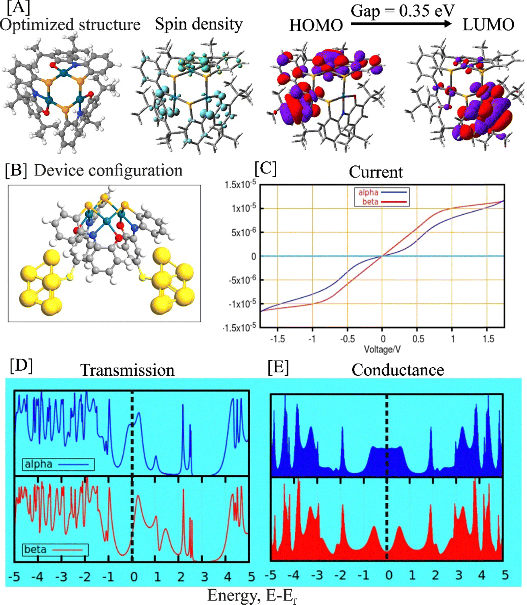 | ||
| Fig. 2 (A) The DFT optimized structure of the neutral complex (complex 1) along with the spin-density and FMOs at ωB97XD/cc-pVDZ level. (B) Device configuration for the computed transmission characteristics of complex 1 with gold electrodes. The relative variations in: (C) current; (D) electronic transmission; and (E) conductance. The different color plots represent computed parameters for different electronic spins. | ||
The spin-density distribution plot of the complex offered an intuitive understanding of the locations of unpaired electrons within the system. The visual representation of the spin-density map (Fig. 2(A)) displayed two distinct colored regions primarily localized on the ligand centers. The green and cyan colors represented the potential locations of the two different unpaired electronic spins in the system. The broken-symmetry calculations indicated a higher probability of antiferromagnetic coupling between these two different electronic spins. Consequently, the mutual antiferromagnetic interactions between the unpaired electronic could give rise to a possible doublet electronic state in the overall system.
Similarly, the HOMO–LUMO isodensity maps also demonstrated a higher likelihood of ligand-centered redox behavior in complex 1. Additionally, it is essential to note that a smaller HOMO–LUMO gap facilitated easier ligand-based redox processes in the system. We have also calculated the one- and three-electron oxidized species of complex 1. The corresponding HOMO–LUMO gaps for the one- and three-electron oxidized complexes were found to be 0.24 eV and 0.91 eV, respectively. It was observed that the first one-electron oxidation diminished the chemical hardness of the system, thus enhancing the redox capabilities. The HOMO–LUMO gap and chemical hardness are closely related, as the latter measures the resistance of the system to changes in electron density and quantifies the energy required for electron addition or removal. A smaller HOMO–LUMO gap typically corresponds to lower chemical hardness. This implies that a system with a smaller gap requires less energy for electron removal or addition, making it more susceptible to chemical reactions and exhibiting lower chemical hardness. As the HOMO–LUMO gap decreased, one-electron oxidation suited for complex 1. However, the significantly high HOMO–LUMO gap for the three-electron oxidized species restricted further oxidation in the system.
Electronic transport calculations
We have performed density functional non-equilibrium Green's function (DFT-NEGF)25-based calculations to understand the electronic transport through complex 1 that was considered to be placed between two gold electrodes. The structure of the model system and some relevant calculated parameters are reported in Fig. 2(B)–(D). For the convenience of our calculations, we have not considered the terminal tert-butyl groups in complex 1 for our model junction, as depicted in Fig. 2(B).We have observed spin-polarized electronic transmission occurring through the junction and have detected significant variations in the electronic transmissions for α- and β-electrons (blue and red colors, respectively) near the Fermi level. Understanding these changes in electronic behavior near the Fermi level is crucial as they can be experimentally validated.26 Moreover, the electronic conductance pattern exhibited substantial differences between the two spin channels, particularly with a notable increase in electronic conductance for α-electrons compared to β-electrons at the Fermi level. This spin-polarized electronic transmission played a vital role in achieving the memristive behavior of complexes,27 and our theoretical calculations demonstrated valuable insights into the underlying mechanisms.
Memristive complexes operate through a mechanism where charge carriers, such as electrons, become trapped within specific regions or sites in the material.28 Our density functional theory (DFT) calculations indicated the presence of unpaired electron densities in complex 1, which acted as a defect or radical site. These sites can potentially trap external charge carriers based on their spin orientations,28 thereby leading to changes in the resistance state of the complex.
The appearance of the spin-polarized current suggested the likelihood of charge carriers, particularly electrons, being trapped in specific regions or sites within the material.29 This advocated the existence of localized areas or regions in the complex with spin-dependent energy levels or potential landscapes. The unpaired electron densities acted as traps, selectively favoring the capture of electrons with a specific spin orientation. By modulating the spin polarization of the electronic transmission, the complex can selectively trap charge carriers based on their spin orientation, resulting in alterations of its resistance state. This spin-dependent trapping mechanism materialized from the interplay between localized spin-dependent trap states and the spin-resolved density of states in the complex.30
The calculated current–voltage (I–V) plot provided essential insights into the behavior of the complex under external electrical perturbations. The presence of a hysteresis loop in the I–V plots for spin-polarized electronic current is a crucial aspect of understanding memristive behavior.31 It provides valuable information on how the resistance of the complex changes in response to applied voltage. The observed hysteresis loop signified the non-volatile nature of the resistance states, as the complex retained its resistance state even when the power was turned off, thus preserving stored information.
The observed current–voltage behavior is significant for resetting or switching the resistance state, which occurs by releasing trapped charge carriers. External stimuli or adjusted bias conditions facilitate this controlled release process, utilizing spin-dependent mechanisms. By manipulating the spin polarization of the electronic transmission and applying tailored biases or external fields, the complex can selectively release trapped charge carriers based on their spin orientation. The spin-dependent trapping and release of charge carriers in memristive complexes involved intricate interactions between localized spin-dependent trap states, spin-polarized electronic transmission, and external stimuli. The ability to selectively trap and release charge carriers based on their spin orientation enables precise modulation of the resistance state, resulting in the memristive behavior observed in the complex.
Furthermore, the shape and area enclosed by the hysteresis loop represent the energy dissipated during resistance switching. A smaller loop in the complex implies lower energy consumption, making it more energy-efficient. Therefore, the hysteresis loop observed in the I–V plots for spin-polarized electronic transmission was a key feature of memristive behavior. It indicated resistance switching, the presence of bistable and multi-level resistance states, retention of resistance states, non-volatility, and energy efficiency. Ultimately, the theoretical prediction of the electronic spin-dependent memristor properties of complex 1 represents a novel research direction, setting it apart from conventional inorganic memristors where diffusion of ions with inherent nonlinearity persists.
Current–voltage (I–V) characteristics and resistive switching (RS) property
Next, thin-film devices of complex 1 were fabricated by sandwiching the complex between two orthogonal electrodes of ITO and aluminium (Al) (or copper, Cu) (inset of Fig. 3(A)) to study the conventional memristor performance. Fig. 3(A) shows a recorded I–V curve in a loop by sweeping bias voltage from 0 V to +Vmax, to −Vmax and back to 0 V, where Vmax is +3.5 V or +2.5 V for Al or Cu top electrode, respectively. This clearly reflected a sweep direction-dependent conductivity difference with a pinched hysteresis, which is a feature commonly known as resistive switching (RS) for memristor and related applications.32,33 Consistent and highly reproducible RS was observed in the complex 1 device as evidenced by the I–V characteristics obtained by varying Vmax step-by-step from ±2.0 V to ±3.6 V, as represented in Fig. 3(B). This reproducibility was also seen in the device with the Cu top electrode (Fig. S6 in the ESI†). Most interestingly, these I–V curves showed a gradual transition from the off (high resistive state, HRS) to on (low resistive state, LRS) states, thereby strongly indicating electroforming-free operation. Further, it revealed that the conductivity difference between the off and on conducting states increased gradually with the increase of Vmax. To emphasize this, we plotted the HRS and LRS currents at the applied bias voltage of −1.0 V of Al top electrode device for all the Vmax values used and found the conductance difference diverging or increasing significantly, as shown in Fig. 3(C). To claim high-performance memristors, endurance and retention are crucial. Fig. 3(D) and (E) illustrate the endurance and retention results, showing stability over 1300 cycles and 35 minutes, respectively, with no noticeable faults. The high and low resistive states (HRS and LRS) remained distinct and stable throughout the tests, which is emphasized statistically through cumulative probability and Weibull distribution plots, as shown in Fig. S9 in the ESI.† In particular, the extracted Weibull shape factors (Table S3 in the ESI†) show higher values, which indicate prolonged durability, reliability, and lifespan of ISET and IRESET currents. Additionally, various control experiments were conducted to confirm the performance stability of complex 1, accounting for device-to-device and cycle-to-cycle variations as illustrated in Section S1 in the ESI.† These experiments also evaluated the potential application of the devices as resistive random-access memory (ReRAM) with both Al and Cu top electrodes (Fig. S10 in the ESI†). Additionally, we have summarized the performance of complex 1 as a memristor material in Table S4 of ESI,† providing a comparison with previously reported results for various molecular metal complexes found in the literature. This memristor property and data storage capability of a device is essential and is the prerequisite to robustly mimic biological synaptic actions. The above memristor results and the simple cross-bar sandwiched structure are useful for fabricating larger memristor arrays, using bottom electrodes as bit lines and top electrodes as word lines, with the help of microfabrication techniques.34 | ||
| Fig. 3 (A) Current–voltage (I–V) characteristics recorded in a loop for an ITO/(complex 1: PMMA)/M thin film device with arrows denoting the sweep direction. The inset shows a schematic of the device under test with top electrode M as either aluminium (Al) or copper (Cu). The current for the Al electrode device is scaled up by a factor of 40 for comparison with the Cu device. (B) I–V sweeps in a loop of varying ±Vmax showing distinct Ion (low resistive state, LRS) and Ioff (high resistive state, HRS). (C) Variation of LRS and HRS recorded at −1.0 V for the applied ±Vmax starting from 2.0 V to 3.6 V. (D) Endurance for more than 1.3 × 10³ cycles. (E) Retention of states for more than 35 min without any noticeable faults. | ||
Electrical characterizations for mimicking synaptic plasticity
The correlation between a biological synapse, which occurs between a pre-neuron and a post-neuron, and our thin film memristor device, with complex 1 pinched between two metal electrodes, is shown schematically in Fig. 4(A). In biological synapses, the electrical signal transmission strength depends on the amount of neurotransmitter released at the synaptic cleft from the presynaptic vesicles and received by the postsynaptic receptors. This indicates that an almost continuous tuning of a postsynaptic signal is possible. To mimic the synaptic actions, we first recorded the excitatory post-synaptic current (EPSC) and paired-pulse facilitation (PPF) responses, followed by plotting of the PPF index by varying the time interval (dt) between the paired-pulse at the presynaptic terminal as shown in Fig. S11 in the ESI.† This indicated primary synaptic functionalities of our complex 1 memristor device. Next, we recorded temporal current (I) responses by applying consecutive voltage (V) scans, starting from 0 V to +3.0 V, and repeated the test by simply flipping the applied voltage polarity to check the capability of the memristor device for mimicking brain functions as shown in Fig. 4(B). Interestingly, the device exhibited a gradual increase in current after passing every positive voltage scan, which reversed upon applying negative polarity bias scans. This is primarily known as the potentiation (P) and depression (D) of a synaptic weight in terms of channel conductance in our case. This result strongly emphasized the suitability of our memristor device for mimicking more complex brain functions simply by tuning the pulse parameters (vide infra). Accordingly, we performed temporal electrical measurements to record the synaptic weight potentiation and depression (P/D) curve using 1000 consecutive incoming write (W) pulses, followed by 1000 erase (E) pulses at the presynaptic terminal, while the other terminal was used to record the postsynaptic signal or synaptic connection strength using a repetitive reading (R) pulses as shown in Fig. 4(C). The postsynaptic current was observed facilitating gradually after applying the excitatory presynaptic pulses sequentially, as shown in Fig. 4(D), although the amplitude of the input voltage pulse remained the same. Thus, herein, we have also observed potentiation and the results were found to be coherent with the learning experience in psychology. Similarly, our devices exhibited memory loss or depression, as evidenced in psychological forgetting events when consecutive inhibitory pulses were administered at the presynaptic terminal. Memory loss or depression was observed as the decrement in the postsynaptic current, as projected in Fig. 4(D). Hence, these results consolidated the capability of the devices to mimic synaptic actions and find applications in the future for the hardware implementation of neuromorphic computing.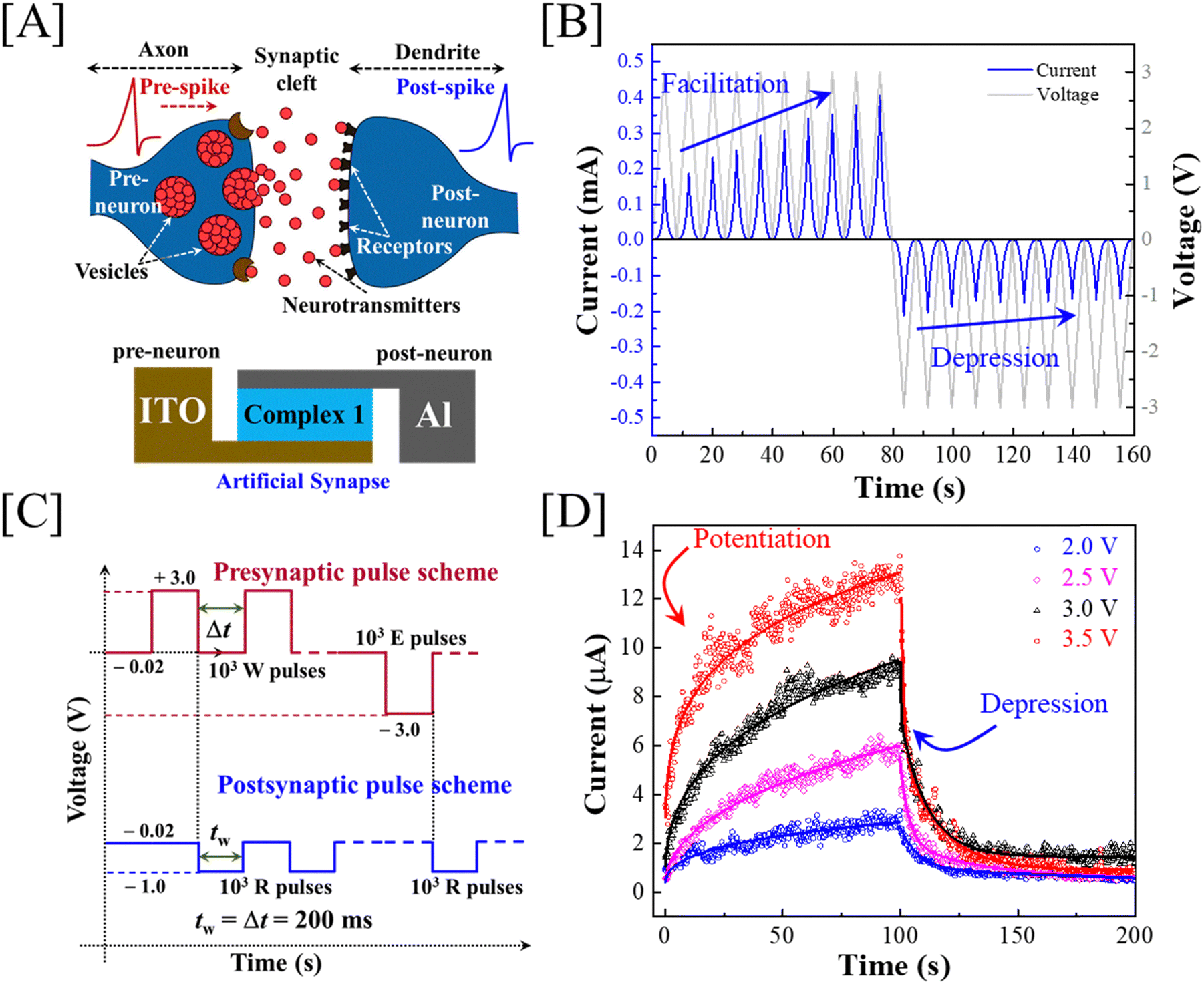 | ||
| Fig. 4 (A) Schematic representation depicting an analogy between a biological synapse and the memristor of complex 1. (B) Temporal current and voltage characteristics demonstrating the potentiation and depression of synaptic weight upon applying consecutive voltage scans. (C) (Top panel) Programmed pulse scheme to record the potentiation (P) and depression (D) curves by applying 1000 write pulses (+3.0 V, 200 ms) and 1000 erase pulses (−3,0 V, 200 ms) at the presynaptic terminal, respectively. A delay of 200 ms is maintained between two consecutive pulses. (Bottom panel) Scheme of postsynaptic reading pulses (−1.0 V, 200 ms) to record the current response. (D) Potentiation (P) and depression (D) curves of synaptic weight change were recorded with the pulsing scheme of (C) by varying the W/E pulse amplitudes as indicated by the legends. | ||
Artificial neural network-based pattern recognition performance
A perceptron neural network with the input layer and output layer directly connected to each other was simulated using the conductance data extracted from the P/D characteristic of presynaptic pulse voltage ±2.0 V (Fig. 4(D)) using an off-chip training procedure.35 A supervised learning algorithm was adopted to identify handwritten digits from the Modified National Institute of Standards and Technology (MNIST) dataset.36 All the simulations were performed using the Pytorch deep learning package.37 The artificial neural network (ANN) has 784 input neurons, which corresponded to the linearized MNIST images with 28 × 28 pixel resolution and greyscale composition. The output of the ANN had 10 neurons, which corresponded to the 10 digits from “0” to “9”. Fig. 5(A) shows the schematic of the perceptron-based ANN which was used for the simulations. Briefly, the pixel values of the MNIST images were first linearized into 784 input neurons, which then underwent vector-matrix multiplication (VMM) with the corresponding synaptic weights and were summed at each of the output neurons.38 For each output neuron, the summed-up input signal was then transformed using a non-linear activation function called the rectified linear unit (ReLU) function. The output thus generated from each of the output neurons was then compared with the image labels during training. The difference between the actual label value and the predicted value was computed using a cost function or loss function. Here, we used the mean cross-entropy loss function as the cost function. The gradient of the as-computed loss function with respect to the synaptic weights was then used to adjust the weight values using a learning methodology referred to as the stochastic gradient descent (SGD) algorithm.39 This whole process of computing the gradients and adjusting the weights based on SGD is called as the backpropagation process. This process was repeated for the whole set of training data (60000 images) after dividing the dataset into multiple batches of data for efficient data handling using a graphical processing unit (GPU). Here, we used a batch size of 32. Each full pass of the training data was referred to as a single epoch. After every epoch, the performance of the ANN was tested using unseen data referred to as the test data (10000 images). The final accuracy of the ANN was computed using the number of correct predictions from the test data. After several epochs of training, we observed that the final test accuracy achieved a reasonably high value. Once the full training process was completed in the purely software-based simulations, the trained weight values were mapped to the device conductance values extracted from the LTP/LTD measurements using a post-training quantization process and subsequent differential pair weight mapping.40,41 The differential pair weight mapping method uses a pair of positive (G+) and negative (G−) conductance values to map the effective conductance to the hardware sense synapse array. The mapped weights were then used to evaluate the test performance of the ANN model. This is referred to as the inference process.
 | ||
| Fig. 5 (A) Schematic of the perceptron-based ANN used for MNIST pattern recognition. (B) Weight map of the output neurons for epochs 1, 5, and 100, respectively. (C) Pattern recognition test accuracy variation with the number of training epochs for both the synaptic device-based and software-based perceptron networks. (D) Effect of MNIST image resolution on the test accuracy. Inset shows the sample images for the digit “5” for various MNIST image resolutions. | ||
Fig. 5(B) shows the evolution of the weight map for each of the output neurons for different epochs. It can be clearly seen that as the training epochs increased, the output neurons were patently distinguishing the distinct features of each of the digits from “0” to “9”. This was a lucid example of the learning behaviour of the synaptic device-based ANN system. A similar trend was also realized for the test accuracy variation with the number of training epochs as shown in Fig. 5(C). The test accuracy increased steadily with the number of epochs, indicating a strong learning behaviour that assisted the ANN in learning distinct features of the input image, thereby distinguishing them from each other. Interestingly, the device-based ANN (92.18%) performed at par with the purely software-based (92.44%) ANN implementation. This can be attributed to the highly optimized nature of the synaptic device and the novel weight mapping method adopted for the hardware ANN implementation.
Furthermore, we have evaluated the performance of the ANN on MNIST data with reduced image resolution. This is a highly significant evaluation method where the effective data storage requirement for the training data can be reduced during hardware implementation. Such low-memory ANN training can be useful in many practical use-case scenarios like IoT sensors, traffic cameras, etc.Fig. 5(D) shows the effect of image resolution downscaling on the ANN test accuracy, and the inset represents the image samples for the digit “5” for various image resolutions. We observed that the device-based ANN retained a test accuracy above 70% until an image resolution of 8 × 8, which was indicative of the low memory requirement of the simulated ANN. Thus, the fabricated synaptic device was best suited for neuromorphic hardware realization.
Conclusions
To conclude, we have successfully synthesized and characterized a triradical-containing trinuclear Pd(II) complex with an St = 1/2 electronic ground state experiencing spin-frustrating-type magnetic coupling amongst the three ligand-based unpaired electrons. These electrons can easily be oxidized or reduced, as evidenced by low oxidation and reduction potentials in the cyclic voltammogram. The complex exhibited memristive properties and can be further used as a sandwich material between two electrodes for neuromorphic computing, hardware realization, and artificial neural network learning. The DFT-based theoretical calculation predicted that the appearance of spin-polarized current due to the presence of an unequal number of organic ligand-based radicals in opposite spins was responsible for the memristor behaviour of the complex.Experimental section
Chemicals and materials
All the used chemicals and solvents were purchased from commercial sources as supplied. Selenium powder, iron powder, 3,5-di-tert-butylcatechol, 2-fluoro-nitrobenzene Pd(OAc)2, ammonium chloride, polymethyl methacrylate (PMMA, average Mw 97000) and dichloromethane (DCM, anhydrous ≥99.8%) were purchased from Sigma Aldrich and used as received without further purification. Other used solvents were obtained from Merck (India). Mass spectra were measured in HPLC grade acetonitrile and methanol solvent. For device fabrication, ITO (∼150 nm) coated on glass substrates having sheet resistance 15 ohm sq−1 were purchased from Optical Filters Ltd, UK. Aluminum (Al) and copper (Cu) pellets (Purity, 99.999%) were purchased from Kurt J. Lesker Company, UK and used to deposit top electrodes with a metal shadow mask using the e-beam or thermal evaporation technique (KJLC PRO Line PVD-75 system).
Physical methods
X-ray crystallographic data were collected at 100 K using Super Nova, Single source at offset, Eos diffractometer. The data refinement and cell reductions were carried out by CrysAlisPro.42 Structures were solved by direct methods using SHELXS-97 and refined by the full matrix least squares method using SHELXL-2018/3.43 All the non-hydrogen atoms were refined anisotropically. SQUEEZE44 operations were performed using WinGX programme to remove disordered solvent molecules. IR spectra were recorded on a PerkinElmer Instrument from 4000 cm−1 to 400 cm−1 at normal temperature as KBr pellets. 1H-, and 13C-NMR spectra of the ligand were recorded in Varian 400 and in BRUKER 600 MHz NMR machines. Cyclic voltammograms (CVs) of the complex were being recorded in dichloromethane solutions containing 0.10 M [(nBu)4N]ClO4 as supporting electrolyte at a glassy carbon working electrode, a platinum wire counter electrode, and a Ag/AgCl reference electrode. The experiments were performed at different scan rates. Ferrocene was used as the internal standard, and potentials are referenced versus the ferrocenium/ferrocene (Fc+/Fc) couple. The cross-sectional SEM image was recorded by field-emission scanning electron microscopy (FE-SEM) using an FEI Nova NanoSEM 450 Field Emission microscope.Device fabrication
Solutions of complex 1 were prepared in dichloromethane (DCM) with a concentration of 5 mg mL−1. PMMA solution was prepared by dissolving 15 mg of PMMA in 1 mL of DCM and stirred for about 30 minutes (until PMMA is completely dissolved in DCM). For device fabrication, sample solution and PMMA solution in DCM were taken in equal volume ratio and the resultant blend solution was stirred for about 1 hour and subsequently used for thin film formation of the active layer. Standard cross-bar two-terminal devices were fabricated wherein ITO-coated glass served as substrates. An ITO strip of width ∼3 mm and ∼150 nm thick was etched chemically employing the standard reported wet etching technique using Zn dust and 1 M HCl, and this acted as the bottom electrode. Subsequently, the patterned glass substrates were subjected to a standard step-by-step cleaning protocol, which involved sequential ultra-sonication in a soap solution, deionized (DI) water, acetone, and ethanol for 10 minutes, with each step repeated three times. Finally, the substrates were rinsed thoroughly in DI water and dried using an air gun. Before thin film formation, the substrates were treated in UV-ozone cleaner for 15 minutes with an emissivity of 95% to eliminate unwanted organic contaminants and stored in a clean and dry environment. The active layer was prepared by spin coating the blend solution containing the sample and PMMA at 1000 rpm for 1 minute, followed by a drying step at 2000 rpm for 30 s. The obtained thin film of thickness ∼100 nm (cross-sectional SEM image in ESI,† Fig. S5) was annealed at 120 °C for 1 hour over a hotplate under ambient conditions, followed by annealing at 80 °C overnight inside a vacuum oven at a 10−2 torr pressure. Then, 60 nm thick and 1.0 mm wide aluminium (Al) or copper (Cu) electrodes were deposited using KJLC PVD-75 PROLine system (e-beam method) at a chamber pressure <3 × 10⁻⁶ torr with a deposition rate of 1 Å s−1 through a metal shadow mask, and these served as top electrodes. Therefore, an active area of the fabricated device, defined as the overlapping area between the top (Al or Cu) and bottom electrode (ITO), was about 3 mm2. The device schematics is as shown in the inset of Fig. 3(A).Electrical characterization for resistive switching (RS) and mimicking synapse
Current–voltage (I–V) measurements were performed using a Keithley 4200-SCS Parameter Analyzer by connecting the bottom ITO electrode to the ground potential. I–V data was obtained for the devices by sweeping bias across 0 V in loops. The voltage was swept to +Vmax (starting at 0 V) then to −Vmax and back to 0 V in steps of 10 mV, the executed I–V measurement is generally termed as a voltage list sweep. To draw further insights into the RS property, the maximum bias voltage (Vmax) was varied from 2.4 V to 3.6 V for the device with Al top electrode (1.0 to 3.0 V for the Cu top electrode device) at both the polarities for successive voltage sweeps. The RS property in the fabricated devices possessed the signature of an artificial synapse. Not only that the I–V characteristics were also recorded for both the voltage sweep directions.To measure the ReRAM device fabricated with either an Al (or Cu) top electrode, a write (W) voltage pulse with an amplitude of +2.0 V (+1.0 V) and a duration of 100 ms was applied to switch the device to the low resistance state (LRS). This was followed by five read (R) pulses of −0.1 V (+0.1 V), each lasting 100 ms with an interval of 100 ms between pulses to probe the LRS state. An erase (E) voltage pulse of −2.0 V (−1.0 V) for 100 ms was then applied to switch the device back to the high resistance state (HRS), followed by another set of five read pulses to complete the “W/R/E/R” cycle. For retention measurements of the LRS conductivity, a write (W) voltage pulse of +2.0 V (+1.0 V) for 100 ms was used to set the LRS for devices with an Al (or Cu) top electrode. The state was then probed using read (R) pulses of −0.1 V (+0.1 V), each lasting 100 ms with a 1-second interval between pulses. To probe the retention of the HRS conductivity, an erase (E) pulse of −2.0 V (−1.0 V) for 100 ms was applied, followed by conductivity measurements using read pulses of −0.1 V (+0.1 V), each lasting 100 ms with a 1-second interval between pulses.
To demonstrate the synaptic functionality of the device, temporal current and voltage characteristics were obtained by performing standard two-terminal I–V measurements as mentioned above for multiple cycles wherein the Vmax was set to 3.0 V to avoid potential damage due to voltage stress. The devices were then subjected to a pulse train as shown in Fig. 4(C), comprising of 1000 presynaptic excitatory voltage pulses and 1000 presynaptic inhibitory voltage pulses having amplitude and pulse width of +3.0 V, 200 ms and −3.0 V, 200 ms respectively. The current measured after the application of a presynaptic excitatory voltage pulse is termed as excitatory postsynaptic current (EPSC) and that after an inhibitory voltage pulse is termed as inhibitory postsynaptic current (IPSC). To probe the EPSC and IPSC response, a postsynaptic pulse of −1.0 V, 200 ms was used after every incoming input pulse. Similar EPSC and IPSC responses were recorded for varying presynaptic pulse amplitudes.
Computational details
The computational simulations are performed using the Gaussian 1645 package. The optimizations are done at the ωB97XD46/cc-PVDZ level. The advantage of using long-range corrected RS-functionals is the range separation parameter ω, provides a better description of the charge transfer prospect in the calculations.46 We used all-electron basis sets (cc-PVDZ), including transition metal atoms, for consistent calculations. Electronic transport was analyzed using the Artaios code,47,48 a post-processing tool combining nonequilibrium Green's function (NEGF) with DFT for Gaussian calculations. Gold electrodes were represented by a triangular-shaped non-periodic Gold(111) surface with 9 atoms connected to the system via a thiol (–SH) bridge. Previous reports indicate that the choice of anchoring units has minimal impact on the fundamental electronic transmission through a molecular junction.49 Additional information about the Artaios code and its theoretical background can be found elsewhere.47Synthesis of [C60H72N3O3Se3Pd3], complex 1
To a suspension of H4LSe(AP) (0.150 g, 0.20 mmol) in acetonitrile (7 mL), Pd(OAc)2 (0.090 g, 0.40 mmol) and Et3N (0.1 mL) were added with continuous stirring. The color of the solution instantly turned into deep brown. It was continued to stir at room temperature for 5 h. A brown precipitate appeared. It was filtered and washed with acetonitrile. X-ray standard single crystals were grown from a mixture of chloroform–acetonitrile solvents (1:1). Yield: 0.164 g, 85%. FTIR (KBr pellet cm−1): 3433, 3051, 2955, 2905, 2866, 1632, 1584, 1517, 1450, 1448, 1407, 1385, 1362, 1341, 1322, 1303, 1273, 1250, 1202, 1173, 1027, 993, 912, 877, 822, 775, 745, 716, 659, 644, 599, 541. [C60H72N3O3Se3Pd3 + H]+: calcd, 1441.05; found, 1441.02; anal. calcd for C60H72N3O3Se3Pd3·CHCl3·0.6H2O: C, 46.66; H, 4.76; N, 2.67, found: C, 46.58; H, 4.62; N, 2.51.
Author contributions
The manuscript was written through contributions of all authors and all authors have approved the final version of the manuscript.Data svailability
The data that support the findings of this study are available from the corresponding author upon reasonable request.Conflicts of interest
The authors declare no conflict of interest.Acknowledgements
PS and CJ are indebted to IIT Guwahati for the doctoral fellowship. CM appreciates funding from the Science and Engineering Research Board (SERB), the Government of India, with the grant number CRG/2021/000441. BCD acknowledged the funding support from SERB, grant number CRG/2021/000567.References
- L. F. Abbott and W. G. Regehr, Nature, 2004, 431, 796–803 CrossRef CAS PubMed.
- H. Yu, H. Wei, J. Gong, H. Han, M. Ma, Y. Wang and W. Xu, Small, 2021, 17, 2000041 CrossRef CAS PubMed.
- S. Choi, S. H. Tan, Z. Li, Y. Kim, C. Choi, P.-Y. Chen, H. Yeon, S. Yu and J. Kim, Nat. Mater., 2018, 17, 335–340 CrossRef CAS.
- A. Mukherjee, S. Sagar, S. Parveen and B. C. Das, Appl. Phys. Lett., 2021, 119, 253502 CrossRef CAS.
- J. Zhu, T. Zhang, Y. Yang and R. A. Huang, Appl. Phys. Rev., 2020, 7, 011312 CAS.
- S. Sagar, K. U. Mohanan, S. Cho, L. A. Majewski and B. C. Das, Sci. Rep., 2022, 12, 3808 CrossRef CAS PubMed.
- H. Chen, Y. Cai, Y. Han and H. Huang, Angew. Chem., Int. Ed., 2024, 63, e202313634 CrossRef CAS PubMed.
- Y. van de Burgt, A. Melianas, S. T. Keene, G. Malliaras and A. Salleo, Nat. Electron., 2018, 1, 386–397 CrossRef.
- L. Yuan, S. Liu, W. Chen, F. Fan and G. Liu, Adv. Electron. Mater., 2021, 7, 2100432 CrossRef CAS.
- L. T. Manamel, S. C. Madam, S. Sagar and B. C. Das, Nanotechnology, 2021, 32, 35LT02 CrossRef CAS PubMed.
- D. Kuzum, S. M. Yu and P. S. H. Wong, Nanotechnology, 2013, 24, 382001 CrossRef PubMed.
- T. Lim, S. Lee, J. Lee, H. Choi, B. Jung, S. Baek and J. Jang, Adv. Funct. Mater., 2023, 33, 2212367 CrossRef CAS.
- B. C. Das, S. K. Batabyal and A. J. Pal, Adv. Mater., 2007, 19, 4172–4176 CrossRef CAS.
- K. A. Rokade, D. D. Kumbhar, S. L. Patil, S. S. Sutar, K. V. More, P. B. Dandge, R. K. Kamat and T. D. Dongale, Adv. Mater., 2024, 36, 2312484 CrossRef CAS.
- S. Parveen, L. T. Manamel, A. Mukherjee, S. Sagar and B. C. Das, Adv. Mater. Interfaces, 2022, 9, 2200562 CrossRef CAS.
- V. K. Sangwan, H.-S. Lee, H. Bergeron, I. Balla, M. E. Beck, K.-S. Chen and M. C. Hersam, Nature, 2018, 554, 500–504 CrossRef CAS PubMed.
- S. Goswami, D. Deb, A. Tempez, M. Chaigneau, S. P. Rath, M. Lal, Ariando, R. S. Williams, S. Goswami and T. Venkatesan, Adv. Mater., 2020, 32, 2004370 CrossRef CAS PubMed.
- S. Sinha, E. M. Sahad E, R. Mondal, S. Das, L. T. Manamel, P. Brandão, B. de Bruin, B. C. Das and N. D. Paul, J. Am. Chem. Soc., 2022, 144, 20442–20451 CrossRef CAS PubMed.
- P. Sarkar, T. J. Konch, T. Kamilya, K. Raidongia, S. Acharya and C. Mukherjee, Chem. Commun., 2020, 56, 15220–15223 RSC.
- P. Sarkar, A. Sarmah and C. Mukherjee, Dalton Trans., 2022, 51, 16723–16732 RSC.
- M. K. Mondal and C. Mukherjee, Dalton Trans., 2016, 45, 13532–13540 RSC.
- A. Rajput, A. K. Sharma, S. K. Barman, A. Saha and R. Mukherjee, Coord. Chem. Rev., 2020, 414, 213240 CrossRef CAS.
- P. Chaudhuri, C. N. Verani, E. Bill, E. Bothe, T. Weyhermüller and K. Wieghardt, J. Am. Chem. Soc., 2001, 123, 2213–2223 CrossRef CAS PubMed.
- S. Kokatam, T. Weyhermüller, E. Bothe, P. Chaudhuri and K. Wieghardt, Inorg. Chem., 2005, 44, 3709–3717 CrossRef CAS.
- M. D. Ganji and F. Nourozi, Phys. E, 2008, 40, 2606–2613 CrossRef CAS.
- R. Warren, A. Privitera, P. Kaienburg, A. E. Lauritzen, O. Thimm, J. Nelson and M. K. Riede, Nat. Commun., 2019, 10, 5538 CrossRef CAS.
- Y. V. Pershin and M. Di Ventra, Phys. Rev. B: Condens. Matter Mater. Phys., 2008, 78, 113309 CrossRef.
- L. A. Pastur, V. V. Slavin and A. V. Yanovsky, Low Temp. Phys., 2020, 46, 724–733 CrossRef CAS.
- P. H. Pereira, A. T. Bezerra, P. F. Farinas, M. Z. Maialle, M. H. Degani and N. Studart, J. Phys. D: Appl. Phys., 2017, 50, 135105 CrossRef.
- L. Wang, C. Yang, J. Wen, S. Gai and Y. Peng, J. Mater. Sci.: Mater. Electron., 2015, 26, 4618–4628 CrossRef CAS.
- Y. Li and M. Xu, Mechanics of Time-Dependent Materials, 2007, vol. 11, pp. 1–14 Search PubMed.
- P. Saha, E. M. Sahad, S. Sathyanarayana and B. C. Das, ACS Nano, 2024, 18, 1137–1148 CrossRef CAS.
- A. Thomas, P. Saha, E. M. Sahad, K. N. Krishnan and B. C. Das, ACS Appl. Mater. Interfaces, 2024, 16, 20693–20704 CAS.
- Y. Yu, M. Xian, D. Fieser, W. Zhou and A. Hu, J. Mater. Chem. C, 2024, 12, 3770–3810 RSC.
- K. U. Mohanan, S. Cho and B.-G. Park, Nanoscale Res. Lett., 2022, 17, 63 CrossRef.
- Y. Lecun, L. Bottou, Y. Bengio and P. Haffner, Proc. IEEE, 1998, 86, 2278–2324 CrossRef.
- B. Steiner, Z. DeVito, S. Chintala, S. Gross, A. Paske, F. Massa, A. Lerer, G. Chanan, Z. Lin and E. Yang, Pytorch: An imperative style, high-performance deep learning library. 2019.
- K. Udaya Mohanan, S. Cho and B.-G. Park, Appl. Intell., 2023, 53, 6288–6306 CrossRef.
- S. Ruder, arXiv, 2016, preprint, arXiv:1609.04747 DOI:10.48550/arXiv.1609.04747.
- V. Joshi, M. Le Gallo, S. Haefeli, I. Boybat, S. R. Nandakumar, C. Piveteau, M. Dazzi, B. Rajendran, A. Sebastian and E. Eleftheriou, Nat. Commun., 2020, 11, 2473 CrossRef CAS PubMed.
- M. Prezioso, F. Merrikh-Bayat, B. D. Hoskins, G. C. Adam, K. K. Likharev and D. B. Strukov, Nature, 2015, 521, 61–64 CrossRef CAS PubMed.
- O. D. L. CrysAlisPro, Version 1, 171. 33. 34d [release 27-02-2009 CrysAlis 171. NET] Search PubMed.
- G. M. Sheldrick, Acta Crystallogr., Sect. C: Struct. Chem., 2015, 71, 3–8 Search PubMed.
- L. J. Farrugia, J. Appl. Crystallogr., 2012, 45, 849–854 CrossRef CAS.
- M. J. Frisch, G. W. Trucks, H. B. Schlegel, G. E. Scuseria, M. A. Robb, J. R. Cheeseman, G. Scalmani, V. Barone, B. Mennucci, G. A. Petersson, H. Nakatsuji, M. Caricato, X. Li, H. P. Hratchian, A. F. Izmaylov, J. Bloino, G. Zheng, J. L. Sonnenberg, M. Hada, M. Ehara, K. Toyota, R. Fukuda, J. Hasegawa, M. Ishida, T. Nakajima, Y. Honda, O. Kitao, H. Nakai, T. Vreven, J. A. Montgomery Jr., J. E. Peralta, F. Ogliaro, M. Bearpark, J. J. Heyd, E. Brothers, K. N. Kudin, V. N. Staroverov, R. Kobayashi, J. Normand, K. Raghavachari, A. Rendell, J. C. Burant, S. S. Iyengar, J. Tomasi, M. Cossi, N. Rega, J. M. Millam, M. Klene, J. E. Knox, J. B. Cross, V. Bakken, C. Adamo, J. Jaramillo, R. Gomperts, R. E. Stratmann, O. Yazyev, A. J. Austin, R. Cammi, C. Pomelli, J. W. Ochterski, R. L. Martin, K. Morokuma, V. G. Zakrzewski, G. A. Voth, P. Salvador, J. J. Dannenberg, S. Dapprich, A. D. Daniels, O. Farkas, J. B. Foresman, J. V. Ortiz, J. Cioslowski and D. J. Fox, Gaussian 09, revision C.01, Gaussian, Inc., Wallingford, CT, 2010 Search PubMed.
- J.-D. Chai and M. Head-Gordon, Phys. Chem. Chem. Phys., 2008, 10, 6615–6620 RSC.
- M. Deffner, L. Groß, T. Steenbock, B. Voigt, G. Solomon and C. Herrmann, Artaios—a code for postprocessing quantum chemical electronic structure calculations, Universität Hamburg, 2010 Search PubMed.
- C. Herrmann, G. C. Solomon, J. E. Subotnik, V. Mujica and M. A. Ratner, J. Chem. Phys., 2010, 132, 024103 CrossRef PubMed.
- Y. Tsuji, A. Staykov and K. Yoshizawa, J. Am. Chem. Soc., 2011, 133, 5955–5965 CrossRef CAS PubMed.
Footnotes |
| † Electronic supplementary information (ESI) available: Characterization data of complex 1, Thickness measurement of complex 1, I–V sweeps in a loop of varying ±Vmax, I–V characteristics in 10 consecutive loops in positive and negative bias sweep direction, I–V characteristics in multiple loops for four different devices, ReRAM applicability of the devices, X-ray crystallographic parameters, and optimized coordinates of complex 1. CCDC 2283578. For ESI and crystallographic data in CIF or other electronic format see DOI: https://doi.org/10.1039/d4mh00928b |
| ‡ Authors contributed equally to this work. |
| This journal is © The Royal Society of Chemistry 2025 |