
 Open Access Article
 This Open Access Article is licensed under a Creative Commons Attribution-Non Commercial 3.0 Unported Licence
Spectroscopic matching in semitransparent solar cells with I–Br mixed halide perovskite and DMD electrode
Olfa
Selmi
a,
Antonella
Lorusso
bc,
Marco
Mazzeo
bc,
Jaume-Adrià
Alberola-Borràs
 a,
Rosario
Vidal
a,
Eva M.
Barea
a,
Rafael S.
Sánchez
a,
Iván
Mora-Seró
*a and
Sofia
Masi
*a
a,
Rosario
Vidal
a,
Eva M.
Barea
a,
Rafael S.
Sánchez
a,
Iván
Mora-Seró
*a and
Sofia
Masi
*a
aInstitute of Advanced Materials (INAM), Universidad Jaume I, Av. Sos Baynat s/n, 12071 Castelló, Spain. E-mail: sero@uji.es; masi@uji.es
bDepartment of Mathematics and Physics “Ennio De Giorgi”, University of Salento, Via per Arnesano, 73100, Lecce, Italy
cCNR NANOTEC-Institute of Nanotechnology, 73100 Lecce, Italy
First published on 16th September 2025
Abstract
Balancing light transmittance and power conversion efficiency (PCE) remains a major challenge for semi-transparent perovskite solar cells (ST-PSCs), particularly for applications in building integration and agrivoltaics. In this work, dielectric–metal–dielectric (DMD) electrodes based on WO3/Ag/WO3 as a high-performance alternative to conventional semi-transparent gold (Au) contacts were integrated into bromide-rich formamidinium lead halide perovskites, with a systematic study across halide compositions from pure bromide to pure iodide. The DMD electrodes consistently enhanced photovoltaic performance and optical quality, achieving an average visible transmittance (AVT) of 43.63%, light utilization efficiency (LUE) of 3.05%, and a PCE of 7% for FAPbBr3-based cells. An optimal composition with 47% bromide yielded a balanced performance with 24% of average visible transmittance (AVT), 2.12% LUE and ∼9% PCE. Rather than simply increasing bromide content to widen the bandgap and enhance transparency, this study shows that there is an optimal spectral alignment that maximizes transmittance, photocurrent extraction and color. In addition, replacing Au with WO3/Ag/WO3 significantly reduces the environmental footprint, as confirmed by life cycle assessment. This study highlights a photonic design approach to advancing efficient, sustainable, and visually appealing ST-PSCs for next-generation energy applications.
Hybrid organic–inorganic perovskite materials have gained emphasis in worldwide photovoltaic (PV) research, particularly due to their impressive power conversion efficiencies (PCEs) above 26% as well as their potential to become a candidate for inexpensive mass production.1–4 The bandgap of perovskite materials can be tuned by altering their composition, allowing for the optimization of light absorption across the solar spectrum.5,6 The peculiarity of the semitransparent solar cell (ST-PSC) is that it should efficiently convert the absorbed light into electrical energy while allowing a significant portion of light to pass through. To achieve that, a balance between optical transparency and electrical efficiency must be maintained.7 ST-PSCs have sparked significant interest owing to their versatile applications across various domains, including building-integrated photovoltaics (BIPVs), tandem devices, skylights, and wearable electronics.8,9 These applications demonstrate the versatility and potential of ST-PSC to integrate renewable energy generation into various aspects of daily life, infrastructures, and technology. A direct and practical way to enhance transparency is by deliberately reducing the thickness of the perovskite film to around 200 nm.10 However, this approach has two major drawbacks: first, it decreases device performance, resulting in lower open-circuit voltage (Voc) and short-circuit current density (Jsc) due to the extreme thinness of the film; second, it introduces challenges in the fabrication of thin films during industrial production.11 Moreover, various strategies have been explored to enhance the AVT, including reducing the perovskite coverage on the substrate and utilizing low-reflecting electrodes, such as low-dimensional materials or highly doped transparent semiconductors. However, these approaches are typically costly, environmentally unfriendly, and can lead to instability or damage to the perovskite layer. Additionally, transparent conducting oxides (TCOs), including indium tin oxide (ITO) and fluorine-doped tin oxide (FTO), have been integrated into optoelectronic devices as transparent electrodes due to their excellent optoelectronic properties and reliable reproducibility.12,13 However, TCOs are not ideal for use as top electrodes because their fabrication requires vacuum processing and high-temperature post-treatment (over 300 °C), which can damage the perovskite layer.14 Moreover, TCOs generally exhibit lower conductivity compared to metal electrodes and have poor mechanical properties, making them unsuitable for such kind of optoelectronic devices.15
Nonetheless, achieving both high transparency and high efficiency in these materials remains a challenging task for semi-transparent perovskite solar cells.16 It has been demonstrated that incorporating dielectric–metal–dielectric (DMD) low reflecting contacts in ST-PSCs offers a superior alternative to solely reducing the thickness of the perovskite film. Instead of employing a conventional metal film, the DMD structure has emerged as a preferred choice for integrating into ST-PSCs, offering advantages in both device transmission and efficiency.17,18 Moreover, the dielectric layers can protect the metal layer from oxidation and other environmental degradation, enhancing the durability and operational stability of the solar cells. An ideal transparent electrode must exhibit high transparency, strong chemical stability, efficient charge collection, low sheet resistance, and low cost. The DMD electrodes allow a balance between optical transparency and electrical conductivity.19 This is critical for ST-PSCs where both high light transmission and efficient charge collection are required.20 The semitransparent nature of DMD electrodes helps in optimizing the light absorption in the active layer of the solar cell, which is essential for achieving high PCE along with high transmittance. Recent developments in semitransparent solar cell architectures have increasingly adopted DMD multilayer electrodes due to their superior combination of optical transparency and electrical conductivity. Several works demonstrated a MoO3/Ag/WO3 DMD structure achieving ∼73% AVT and low sheet resistance (∼7 Ω sq−1), making it highly suitable for semitransparent perovskite solar cells.17,21 Expanded on this approach by combining modeling and experiments in order to optimize optical performance in WO3/Ag/WO3 and electrodes. Their strategy achieved >90% average transmittance across 300–800 nm and boosted device photocurrent and PCE by 45% and 12%, respectively, compared to standard ITO/Ag contacts. MoO3/Ag/WO3 structures enabling transparency tuning without significantly sacrificing performance, especially suitable for neutral-color windows and LED technologies.22 These diverse approaches emphasize the growing role of DMD engineering in enabling efficient, scalable, and visually integrated solar technologies. In this study, the WO3 was selected as the intermediate layer between the hole transport layer and the metal layer. Since the electrical characteristics of DMD electrodes are primarily influenced by the metal layer, Ag has been used due to its high conductivity.17 As well as, WO3/Ag/WO3 configuration demonstrated superior transmittance compared to the MoO3/Ag/MoO3 configuration, particularly within the 600–800 nm wavelength range.23,24 Additionally, the upper dielectric layer WO3 with its high refractive index minimizes light reflection from the electrode, thereby increasing overall transparency. The selection of WO3/Ag/WO3 is based on its low sheet resistance of around 10 Ω sq−1,24,25 the efficient hole extraction facilitated by the WO3 work function of 4.8 eV (ref. 26) and the lower diffusion rate of Ag through the dielectric compared to other metals like gold (Au) or copper (Cu), which contributes to improved device stability.27
In a previous work, an unmixed FAPbI3-based perovskite device with a WO3/Ag/WO3 electrode achieved a PCE of 16.2% and an AVT of 22.5%, resulting in an LUE of 3.7%.17 This work highlights the focus on pure iodide perovskites; however, studies on the universal applicability of the DMD in mixed halide perovskites with varying anion compositions, i.e., different band gaps, are still underrepresented. In response to these challenges, this study explores the use of DMD electrodes in solar cells with I–Br mixed halide perovskite as active layers. A characterization at 0° and 45° light inclination angles was conducted, comparing DMD and gold as top electrodes and utilizing various perovskite compositions as active materials. Notably, when using DMD contact, FAPbI3 achieved a PCE of 14.7%, an AVT of 5.84%, and an LUE of 0.85%. Although the AVT of FAPbI3 is relatively low, FAPbBr3 based devices achieved a high AVT of 43.63%, a PCE of 7% and an LUE of 3.05%. Nevertheless, the chromaticity coordinates (a* and b*) of the pure bromide perovskite deviate more significantly from neutrality compared to those of the mixed halide perovskite. To address this trade-off between transparency, efficiency, and color neutrality, a bromide content of 47% was identified as the optimal composition to balance these parameters, resulting in an AVT of up to 24%, an LUE of 2.12%, and a PCE of approximately 9% with chromaticity coordinate closer to neutrality, ensuring a natural and visually pleasing appearance, which is suitable for building-integrated photovoltaics. This demonstrates that aligning the optical properties of the perovskite with those of the DMD yields the most favorable outcomes. The most interesting aspect of this study is the improved efficiency of solar cells when using DMD contacts compared to conventional semi-transparent gold contacts. This is mainly attributed to an increase in the short-circuit current density. The improvement of the light harvesting is in fact due to the higher transmittance and the low refractive index of DMD. Additionally, the chromaticity coordinates for the fully semitransparent devices using DMD were closer to neutrality compared to those of the pure perovskite films, while at the same time, current and aesthetic parameters are increased to real building-relevant values. Moreover, the sustainability of the DMD electrode has been studied, resulting in a prominent advantage compared with the Au electrode.
1. Results
1.1. Concept of semi-transparent electrode engineering by spectroscopic ellipsometry
The development of DMD transparent electrode is intended to overcome the known challenges of established semi-transparent approaches while at the same time increasing the aesthetic parameters of the ST-PSCs to a market-acceptable level. The DMD electrode is engineered by preliminary procedures consisting of the deposition of a dielectric layer on glass that is glass/WO3 (D), dielectric and metal layers on glass that is glass/WO3/Ag (DM), and finally the dielectric–metal–dielectric layers on glass that is glass/WO3/Ag/WO3 (DMD). The transmittance spectra are shown in Fig. 1a, where the DMD transmittance reaches a maximum value of 82% exceeding the transmittance of the single D in the wavelength range from 450 nm to 500 nm.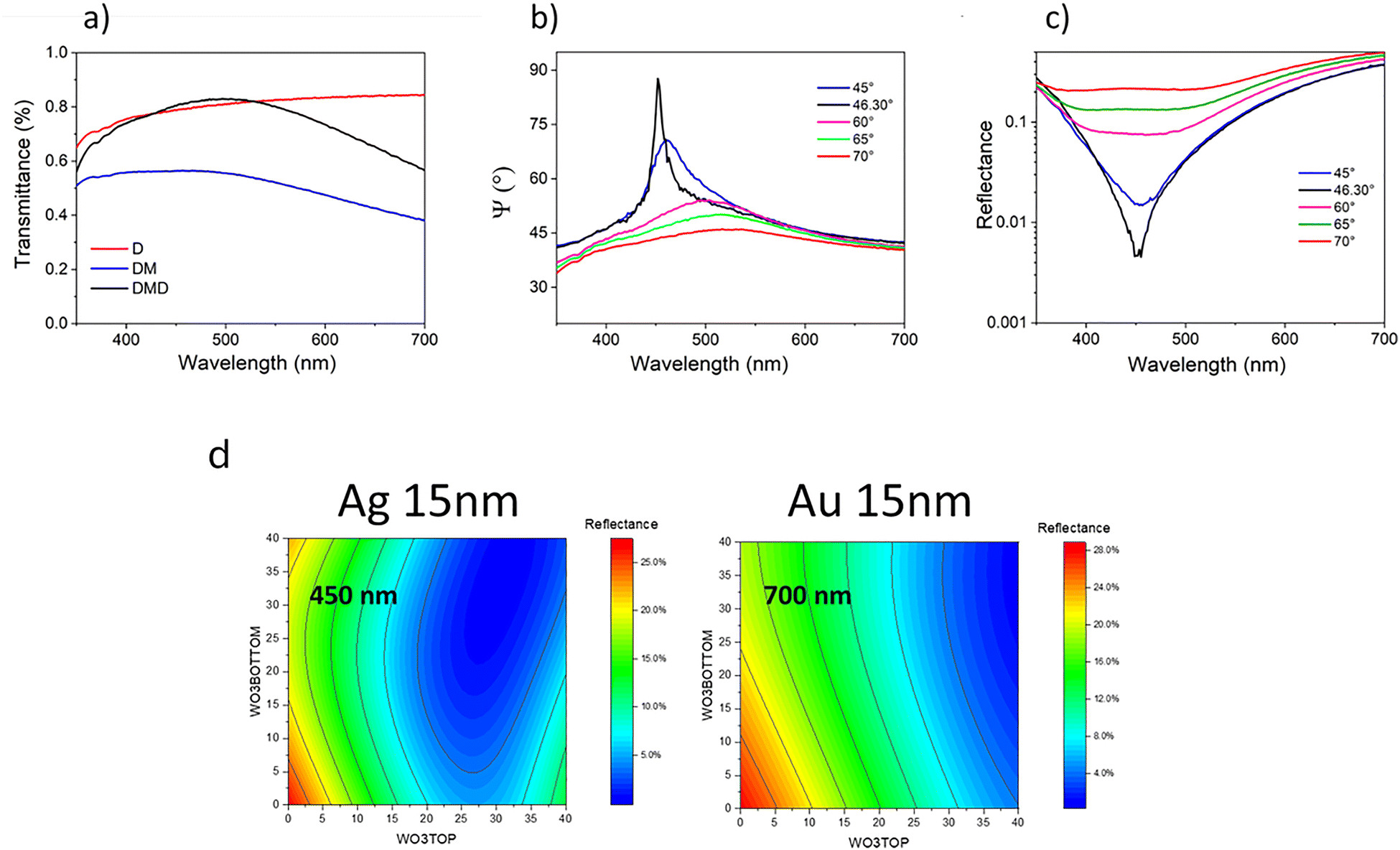 | ||
| Fig. 1 (a) Transmittance spectra of produced D, DM, and DMD structures, acquired at normal incidence as a function of the incident wavelength. (b) Ellipsometric data of the Ψ phase of DMD40 at different angles of the incident light. (c)Total reflectance of DMD40 at different angles of the incident light. (d) The simulation maps of reflectance for different thicknesses of bottom and top dielectric layers using silver (Ag) and gold (Au), respectively. | ||
Moreover, the optical dispersion data are obtained using CompleteEASE spectroscopic ellipsometry and applied in a theoretical model to determine the optimal thickness of the DMD architecture for minimizing reflectance. In a previous paper, we demonstrated that the dielectric thickness of 40 nm, named DMD40, shows that the ellipsometric phase approaches 90° at the incident angle of the light corresponding to 46.30° and at a specific wavelength of 450 nm, see Fig. 1b.17 This feature affects the transversal electric, TE or s, and magnetic, TM or p, modes of the reflected light, since  , with the consequence that the reflected s mode vanishes, as well as a very low p mode, guarantying an almost zero total reflectance, and in turn high transmittance, see Fig. 1c. The antireflection conditions of DMD40 have been used to realize the cathode for the ST-PSCs.
In contrast, the introduction of a gold layer in the DMD structure results in minimal reflectance at 700 nm, which falls outside the visible spectral range, while the Ag layer determines the antireflection conditions in the visible range, particularly around 450 nm. The simulation maps of reflectance for different thicknesses of bottom and top dielectric layers are reported in Fig. 1d. The reason for this behavior lies in the real part of the refractive index of Au that becomes negligible at wavelengths larger than 650 nm, while it is negligible in the whole visible spectrum for Ag, due to the plasmon frequency.
1.2. Semitransparent perovskite solar cells and aesthetic parameters
In this work, the perovskite is prepared by mixing precursor materials, e.g., CsI, FAI, PbI2, and PbBr2, in a desired molar ratio to obtain mixed anion halide perovskite, see Fig. 2a. By increasing the bromide content, a blue shift was observed. This blue shift indicates a wider band gap of the perovskite film and greater transparency.28–31 This consequently allows more light to pass through the perovskite film. The pure iodide perovskite composition exhibits a dark brown color, transitioning to red with the increase of bromide concentration and turning orange for pure bromide, wherein the band-gap shifts from Eg = 1.54 eV (FAPbI3) to Eg = 2.27 eV (FAPbBr3), as illustrated in Fig. 2a and Tauc plot in Fig. S1. | ||
| Fig. 2 (a) UV-Visible absorption spectra of mixed halide FAPbI3−xBrx perovskites thin films with different bromide concentration, (b) corresponding X-ray diffraction (XRD) patterns, (c) zoomed-in XRD pattern highlighting a shift in the peak position (110) with increasing Br content and (d) normalized photoluminescence spectra of mixed halide FAPbI3−xBrx perovskites thin films with different bromide concentration. | ||
To quantitatively define transparency, the AVT was determined by integrating the area under the transmittance curve in the range from 300 nm to 900 nm, see Fig. S2. In this study, the thickness of the perovskite film remains constant, ∼350 nm, see Fig. S3, while we manipulate transparency by adjusting the I: Br ratio. It is noteworthy that an increase in bromide content widens the halide perovskite bandgap, consequently leading to an increase in the AVT from <1% for FAPbI3 to 57.43% for pure bromide films, see Table S1.17
The photoluminescence (PL) and the X-ray diffractions (XRD) are shown in Fig. 2b–d, corroborating the typical formation of the halide perovskite materials.
By increasing the bromide content within the perovskite, a notable enhancement in intensity occurred, see Fig. 2b, alongside a shift in the peak associated to the (110) diffraction towards larger angles, see Fig. 2c. This shift is attributed to the alteration in crystal structure from tetragonal to cubic.32,33 The blue shift in the photoluminescence spectra, see Fig. 2d, with increasing bromide concentration in perovskite films, indicates changes in the bandgap and electronic structure of the material in line with the transmittance spectra.34 As expected.
Morphological characterizations are shown in Fig. S4 and S5, demonstrating low and comparable surface roughness by atomic force microscopy (AFM) for all the samples and uniform coverage by top-view scanning electron microscopy (SEM) images, respectively.
As commented above, in this study, we use WO3/Ag/WO3 as low reflecting electrode to exploit a photonic approach to improve the current generation and in turn the efficiency along with the transparency; furthermore the DMD electrode has several benefits like: the bottom layer of WO3 of 40 nm acts as a seeding layer hindering the reaction between Ag and halide in perovskite film and ensuring a good surface coverage for the Ag thin film 15 nm, which facilitate the formation of a uniform and continuous layer; the top WO3 layer maintains the antireflection of silver and determines the transmission window of the DMD structure.35,36 To demonstrate the high quality of the photonic approach, DMD electrodes and different perovskites (with a thickness of 350 nm, measured by SEM cross section, see Fig. S3) are integrated into ST-PSCs with the device architecture glass/ITO/SnO2/perovskite/spiro-OMeTAD/DMD as illustrated in Fig. 3a (picture of the real device in Fig. 3b). The major advantage of the DMD electrode and characterization at different angles compared with a common metal electrode is given by the fact that the device transmittance is solely defined by the thickness of the employed dielectric and metal, and does not need to be controlled with the perovskite thickness.
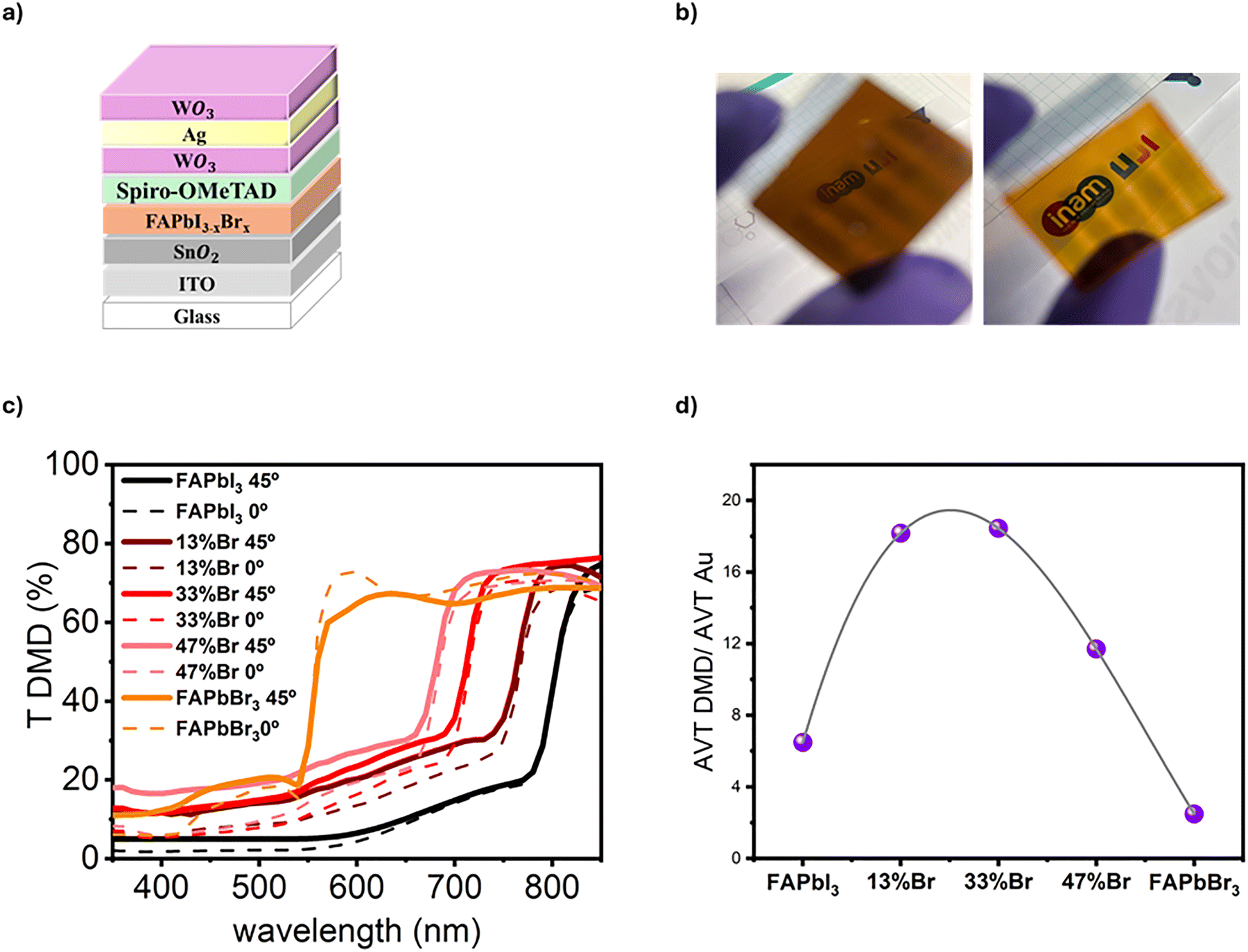 | ||
| Fig. 3 (a) Device architecture of the ST-PSC (glass/ITO/SnO2/perovskite layer/Spiro/WO3/Ag/WO3), (b) a photograph of the as-fabricated ST-PSC of FAPbI3−xBrx with 47% Br (left) and FAPbBr3 (right) showing a good transparency, (c) transmittance spectra of ST-PSC devices with DMD at normal incidence and 45° light inclination and (d) the ratio of ST-PSC devices transmittance between DMD and Au versus bromide composition at 45° light inclination. | ||
The transmittance spectra of the semi-transparent perovskite solar cells with DMD contact at 0° and 45° of light inclination are displayed in Fig. 3c, and the corresponding AVTs have been calculated and are provided in Tables S2 and S3. At normal inclination (0°), by altering the perovskite composition by increasing the bromide content, the AVT increased from 1.40% to 44.35% for FAPbI3 and FAPbBr3, respectively, see Table S2. More importantly, a continuous variation of the transmittance can be achieved by changing the inclination angle of the perovskite with the DMD on top, namely, the complete pixel. At 45° inclination, the AVT increases from 5.84% for the ST-PSC devices based on pure iodine film and maintain a similar value (∼44%) for the ST-PCS devices based on pure bromide film, but increasing significantly for mixed anion compositions, see Table S3, with an enhancement especially at short wavelength, the spectral region in which the bromine perovskite absorbs more. Fig. 3d illustrates the AVT ratio between DMD and gold semitransparent contact at 45° of light inclination. The increasing trend with values greater than 1 proves that devices with DMD electrodes exhibit superior transmittance compared to those with gold contact, which could be attributed to the high refractive index of Au, which prevents light from passing through.37 Notably, this improvement is most pronounced at 13% and 33% bromide concentration, where the ratio reaches approximately 18. This indicates that at these concentrations, the devices with DMD exhibit the greatest transmittance improvement over the Au (30 nm)-based devices, which confirms the higher transmittance and lower refractive index achieved by DMD. This enhancement is also attributed to the optimal balance between absorption and scattering losses and the optimal arrangement of bromide ions within the lattice, which enhances transmittance, suggesting a potentially useful composition for applications requiring high transmittance. Therefore, by changing the electrode, perovskite solar cells with band gaps over a wide range from Eg 1.54 eV (FAPbI3) to Eg = 2.27 eV (FAPbBr3) can easily be made as transparent as a bare film or even better, see Tables S1, S2 and S3. The latter highlights the reduction of the electrode reflectance up to its critical angle as well as the improved transmittance of the perovskite regardless of the thickness and composition. The increase of the AVT of the device's pixels compared to that observed at normal inclination may be attributed to the high transmittance and low reflectance exhibited by the electrode at this critical angle, see Fig. 1a and c. For comparison, the transmittance spectra for reference devices using 30 nm semitransparent Au are also provided in Fig. S6, and the detailed average visible transmittance is listed in Tables S4 and S5. These spectra show a decrease in the transmittance of the pixel with increasing angle of light incident (45°), which can be attributed to the higher back-reflected light.17
As we observed higher transmittance of the device at 45°, we performed the characterization of the solar cells at this inclination. At 45° of light inclination, the DMD-based device efficiencies are higher than the Au control devices. This is mainly attributed to an increase in the short-circuit current densities (Jsc). The improvement of light harvesting is, in fact, due to the decrease of the DMD electrode reflectance.
Consequently, the optical path within the perovskite active layer is effectively increased, enhancing light absorption and thereby directly increasing both Jsc and PCE.38,39 More importantly, with the increase of bromide concentration, the devices with the semi-transparent DMD contact exhibit relatively improved performance and improved current density Jsc. Fig. 4a shows in detail that the PCE DMD/PCE Au% % ratio is greater than 1 for solar cells with more bromide content (namely 47% bromide and pure bromide) in the perovskite composition. This enhancement can be attributed to the favorable optical matching between the DMD and bromide-rich perovskite. Fig. S7 provides the statistical characterization of photovoltaic parameters for devices made with different perovskite compositions and using both Au and DMD contacts at 45° of light inclination. As the concentration of bromide increases, the Voc rises, while conversely, the Jsc decreases as expected.40 Furthermore, the decrease of Jsc correlates directly with the blue shift of the absorption onset, in line with the increase of the band gap,41 as previously discussed. However, the (Jsc DMD/Jsc Au) ratio presented in Fig. 4b is higher than 1 with the increase of Br concentration, indicating that the current density (Jsc) increases when using the DMD contact compared to Au by increasing the Br content. On the contrary, the Voc and the FF show a similar value, with a ratio around 1 (see Fig. 4c and d). Fig. S8 presents the J/V curves of the devices with DMD contact at 0° and 45° of light inclination. This figure illustrates the rise in current density when light is inclined at a 45° angle, while maintaining the same open-circuit voltage (Voc). For FAPbI3, the current density increases from 15.8 mA cm−2 to 19.4 mA cm−2. Similarly, at a 13% Br concentration, the current density rises from 14.34 mA cm−2 to 15.7 mA cm−2. With 33% Br concentration, the current density increases from 12.6 mA cm−2 to 14.8 mA cm−2, and at 47% Br concentration, it increases from 11.1 mA cm−2 to 12.89 mA cm−2. Particularly, the notable enhancement of the current density achieved by the perovskite with pure bromide, from 4.5 mA cm−2 to 7.27 mA cm−2, can primarily be attributed to the increase in light harvesting due to the matching between the transmittance spectrum of the DMD contact in the region going from 400 nm to 600 nm, see Fig. 1a, and the absorption spectrum of the FAPbBr3 within the same region, see Fig. 2a. In the same way, Fig. 1b and c illustrates the decrease of the reflectance of DMD at 45° of light inclination, which is well correlated with the increase of the current density.
 | ||
| Fig. 4 Comparison of the PCE ratio between solar cells fabricated with DMD and Au contacts, including the relevant photovoltaic parameters Jsc, Voc, FF, at 45° of light inclination. | ||
The bromide content significantly affects the absorption spectrum of the perovskite, but the DMD electrode plays a pivotal role in enhancing light harvesting. The transmittance spectrum of the DMD electrode is specifically engineered to align optimally with the absorption spectrum of the mixed-halide perovskite layer. This precise alignment minimizes reflection losses and maximizes light entry into the active layer, thereby boosting particularly the short-circuit current density and improving the overall device efficiency.
To isolate the effect of the DMD electrode, a comparative experiment was conducted using a gold electrode. These devices (with Au contact) exhibited lower current density and lower PCE despite the same perovskite composition. This confirms that the performance enhancement observed with the DMD electrode is not solely due to changes in bromide content but is directly related to the improved optical properties of the DMD structure. As well as the devices with DMD contact exhibit higher transmittance compared to the devices with gold, which indicates the higher transmittance and the lower refractive index of DMD.
The photon-balance check curves for the devices with different perovskite anion compositions using DMD at 45° of light inclination are illustrated in Fig. S9. This figure demonstrates in detail that the enhancement in device transmittance is solely attributed to the antireflection condition achieved by the DMD electrode, as evidenced by the low diffused reflectance (R) shown in the photon-balance check curves. The incident photon to current efficiency (IPCE) is directly influenced by the amount of light absorbed.42 Indeed, the IPCE is the product of the light harvesting efficiency, the charge collection efficiency, and the charge separation efficiency.43 At 45° light inclination, the devices with DMD contact exhibit remarkable IPCE within the visible spectrum, demonstrating robust performance. This observation aligns closely with the findings from the transmittance (T) and absorption analyses. The T + R + IPCE spectra were measured, and the values are below 100% at every wavelength, confirming the consistency of the photon balance as well as the integrated Jsc values for all cells closely correlate with those obtained from J/V measurement, underscoring the reliability of the parameters obtained.44
Fig. S10(a)–(d) illustrates the PL spectra obtained under 100 s of continuous illumination with a laser excitation of 450 nm and a power of 10 mW cm−2. The peak position of the PL remained consistent for all perovskite compositions, indicating that there is no phase segregation. Notably, the absence of halide segregation suggests that ion migration is not occurring under these conditions, further confirming that these perovskite compositions are optically stable and resistant to light-induced halide segregation.
Therefore, excitation powers of 10, 20, 100 and 200 mW cm−2 were applied to the film with 47% bromide concentration, see Fig. S10(e), resulting in a slight red shift in the emission at a higher power of excitation (200 mW cm−2), which indicates the formation of I-rich domains.45,46
Additionally, recent research suggests47 that photoinduced halide segregation can cause a significant loss in current, a reduction in photovoltaic performance, and can accelerate the degradation of perovskite solar cells (PSCs).48 As a result, reducing the rate of halide segregation is a key strategy to enhance the kinetic stability of mixed-halide perovskites.49
The stability of the devices with varying perovskite compositions was evaluated with both gold and DMD under continuous illumination. Fig. S11 illustrates the steady-state current at maximum power point (JMPP), demonstrating excellent stability and indicating that the devices maintain consistent performance after continuous illumination under 1 sun (1000 W m−2) for 1000 seconds. This stability suggests that the devices do not degrade or lose efficiency under prolonged exposure to light, which is in correlation with the PL measurement (Fig. S10) under continuous illumination.
Semi-transparent solar cells are designed not only to generate electricity but also to allow some light to pass through, which can be aesthetically appealing for applications like windows or building facades. In addition to the AVT, it is essential to report crucial metrics for ST-PSC aesthetics, such as the chromaticity coordinate CIELAB (a*, b*) and light utilization efficiency (LUE).
The chromaticity coordinates (a* and b*) values are used to define the position in the color space, which is commonly adopted in the window industry.50,51 The a* coordinate indicates the green-to-red spectrum, while the b* coordinate represents the blue-to-yellow spectrum.47 When the values of both a* and b* are closer to 0, the color appears more neutral (absence of color), making it suitable for building integration as solar windows.52 The challenge here is to achieve good efficiency while maintaining a neutral color. Thus, a* and b* were determined through an analysis of the transmittance spectra. The values for the bare films are summarized in Table S1, and the values of the fully transparent devices with DMD contact at 0° and 45° inclination are calculated and detailed in both Tables S2 and S3, as well as the values for the devices with gold are summarized in Tables S4 and S5. The CIELAB a* and b* values for the devices with DMD are notably lower than those of the bare films. This difference is especially pronounced at 45° inclination, where the a* and b* values for mixed and not mixed halide perovskite with varying compositions show a significant decrease, especially for 47% bromide perovskite composition, as illustrated in Fig. 5a. This reduction suggests that these values are relatively closer to neutrality (see Fig. 5a). To assess the color neutrality of the active layers as well as the semitransparent devices, the color perception indices were calculated within the CIELu’v’1976 color space (see Tables S1–S4), designed to represent human visual color perception.53Fig. 5b further illustrates the CIELuv’ for the net perovskite films and devices incorporating DMD contact at 45° light incidence. The u′ and v′ parameters are quite similar for all devices with varying compositions, with values falling within the range [0.23–0.52], located in the white region.54
 | ||
| Fig. 5 (a) Chromaticity coordinates CIELAB (a*, b*), the rectangular region defines the coordinate range accepted for window Applications (−5 < a* < 1 and −5 < b* < 5),55 (b) uniform chromaticity coordinate (CIELu’v’1976) for the net perovskite films and devices with DMD contact at 45° light incidence. | ||
LUE for ST-PSCs is a critical parameter that measures how effectively these solar cells convert incident light into electrical energy while also allowing a portion of light to pass through.56 This parameter is particularly important for applications where both energy generation and transparency are desired, such as in building-integrated photovoltaics or agrivoltaics.57 It is determined by the product of AVT and PCE (LUE = PCE × AVT).57
Aimed at evaluating the performance of the ST-PSCs, the LUE values are calculated and summarized in Table 1. At a 45° light inclination, the devices achieved 0.85%, 2.16%, 2.35%, 2.13%, and 3.05% for FAPbI3, mixed halide perovskites with 10%, 33%, and 47% Br concentration, and FAPbBr3, respectively. This metric allows for comparing different technologies to their theoretical limits while also indicating overall system efficiency. For example, in applications such as windows or displays, it represents the combined efficiency of power generation and lighting. Specifically, it measures the amount of transmitted light relative to the incident lighting power. A device with high LUE could be used on windows to generate power without obstructing natural light, thereby reducing the need for artificial lighting during the day.58
| Semi-transparent perovskite solar cell | AVT % | PCE% | LUE% | a* | b* |
|---|---|---|---|---|---|
| FAPbI3 | 5.84 | 14.7 | 0.85 | 8.19 | 3.60 |
| 13%Br | 17.81 | 12.18 | 2.16 | 7.19 | 11.64 |
| 33%Br | 19.92 | 11.8 | 2.35 | 9.27 | 13.51 |
| 47%Br | 24.00 | 8.89 | 2.13 | 7.20 | 10.88 |
| FAPbBr3 | 43.63 | 7 | 3.05 | 26.97 | 37.80 |
Further research on more appropriate device architectures, as well as improved absorb quality, is expected to boost the performance of these solar cells employing DMD electrodes to values close to theoretical limits. Our research has achieved with the DMD contact one of the best PCE values with a higher AVT for the pure iodide, the mixed halide perovskite and the pure bromide. The values are summarized in Table 1. Finally, a power conversion efficiencies (PCEs) of 14.7% with a Voc of 1.01 V, FF of 74%, and a Jsc of 19.4 mA cm−2 and a 7% with a Voc of 1.3 V, FF of 80%, and a Jsc of 7.27 mA cm−2 are achieved, for FAPbI3 (AVT 5.84%) and FAPbBr3 (43.63 AVT %) respectively at 45°, where the integrated current from the IPCE measurements matches with the solar simulator data. This represents one of the best reported semitransparent perovskite solar cells with DMD electrode reported so far (record solar cells in literature for FAPbI3 is PCE of 16.2% and AVT 22.5%),17 however, characterized at different angles, unlike previously reported approaches.17
2.3. Life cycle assessment
Moreover, we are very conscious that we need to move into an economy that is renewable and circular and nature positive. Thus, the environmental impacts associated with the deposition process of an electrode comprised of a WO3/Ag/WO3 triple layer using vacuum evaporation, notable for its exceptional transparency, are evaluated using the life cycle assessment (LCA) methodology, conducted by EN-ISO standards (14040/14044) and the IEA PVPS guidelines.59 This evaluation is juxtaposed with that of depositing a gold electrode with low opacity, employing the same vacuum evaporation technique and the same surface. Two scenarios are determined for the treatment of the residues generated during the evaporation: residual landfill and recycling. Life cycle inventories, including raw materials, vacuum deposition, and waste treatment, as well as the evaluation of impacts with the method Environmental Footprint, EF 3.0, are presented in SI2 and Table S6.Transparency of perovskite solar cells is barely analyzed through LCA, with only one reference,60 which assumes, for LCA, a 15-nm silver electrode as a metallization paste composed of silver, organic compounds, and lead, as included in the Ecoinvent database.61 The environmental impacts of electrodes of different materials (gold, silver, aluminum, copper, carbon, etc.) are part of a number of life cycle analyses of PSCs. However, this is the first time that the environmental impact of electrode WO3/Ag/WO3 is studied.62 Upon the deposition of electrodes onto PSCs, it has been observed that the utilization of gold poses a more significant environmental detriment compared to silver.62,63 Gold electrodes have been identified as a noteworthy source of environmental impact in contrast to the entire device.62–67 In addition to its application in PSCs, the use of gold in other contexts as a conductive material holds significant environmental implications, primarily attributable to its extraction through mining processes.68 In the present work, the focus is uniquely set on the deposition of the electrode.
The replacement of gold material with silver and tungsten materials yields a highly beneficial environmental impact, as illustrated in Fig. 6. The DMD electrode, compared to the gold electrode, reduces the impact due to gold substitution in most of the impact categories, although it requires higher electrical energy consumption for vacuum deposition. For the climate change (GW) category, the impact of the DMD electrode relative to the gold electrode is only 15%, which is an environmental improvement of 85%, see Fig. 6a. This improvement is due to the reduction in material impact. In the gold electrode, the impact of materials is 95% of the total, while electricity consumption is only 5%. On the contrary, in the DMD electrode, where the electrical consumption during deposition increases 2.3 times, the impact of materials is 14% and the impact of electricity rises to 86%. The landfilling impact is negligible for both electrodes.
 | ||
| Fig. 6 Comparative environmental assessment of vacuum deposition of WO3/Ag/WO3 and gold electrodes. (a) Global warming potential for the two electrodes for landfilling and recycling, (b) relative impacts, absolute values are in the Table S7, for both electrodes for several impact categories calculated with the method EF 3.0 for the impact categories: global warming (GW), ozone depletion (OD), ionising radiation (IR), photochemical ozone formation (POF), particulate matter (PM), human toxicity non-cancer (HTnC), human toxicity cancer (HTC), acidification (Ac), eutrophication – freshwater (EuF), eutrophication – marine (EuM), eutrophication – terrestrial (EuT), ecotoxicity – freshwater (EcF), land use (LU), water use (WU), resource – fossils (ADf), resource – minerals and metals (ADm). | ||
DMD electrodes exhibit a significant reduction of environmental impacts over the gold electrode due mostly to the reduction of the impact of DMD electrode materials over most of the impact categories, as shown in Fig. 6b. In contrast, the higher electricity consumption in deposition does not compensate for the reduced impact of materials only in the ozone depletion (OD) and water use (WU) categories. In addition, it should be noted that the environmental impact of electricity consumption will be reduced as the electricity mix incorporates a higher percentage of renewable energies.
Material losses during the deposition process are highly significant, approximately 99%. Efforts to recycle these losses offer significant environmental benefits, as depicted in Fig. 6a, with negative values, particularly for the gold electrode. Regarding climate change, the impact of the recycling scenario is 24% less compared to landfill disposal. The calculation of the recycling benefit has been based on average inventories for the treatment of electrical and electronic waste in Europe.69 Although it could be higher if specific recycling were applied solely to waste from the vacuum deposition process.
2. Conclusions
In this work, a DMD electrode to overcome the known challenges of established semitransparent approaches while at the same time increasing the aesthetic parameters of the solar cells to a market-acceptable level is introduced. It is shown that the AVTs increase with the inclination angle in a wide range of perovskite bandgap for FAPbI3 and FAPbBr3 and mixed anion perovskite compositions. Solar cells fabricated based on DMD electrodes and bromide perovskite achieve PCEs as high as 7%, being one of the most efficient semitransparent bromide-based perovskite solar cells reported so far. The best compromise in terms of aesthetics parameters and solar cells efficiency is reached with 47% bromide content achieving an AVT of up to 24%, LUE of 2.12% and a PCE of approximately 9%, as well as this composition also yields chromaticity coordinates values closer to neutrality, demonstrating the matching of the optical properties of the perovskite and the DMD lead to the best results. In addition, the environmental impacts of the DMD electrode are reduced in the most relevant categories, such as global warming, with a reduction of 85%. Further research effort is particularly required to understand and improve LUE (3.05%). Fine tuning of the composition as well as the thickness of the device's layers is expected to be a promising approach toward more transparent devices in the bandgap regime that is more suitable for building integration. In addition, a focus needs to be set on more suitable device architectures and interface modifications specifically developed for bromide perovskite absorbers. Both approaches are expected to boost both transparency and performance of those materials, which, together with the significantly enhanced CIELab coordinates, might enable a future market-competitive semitransparent solar cell.3. Methods
3.1. Materials
No additional purification processes were employed for any of the materials utilized. Formamidinium iodide (FAI, 98% purity, sourced from GreatCell Solar), lead iodide (PbI2, >98% purity, obtained from TCI), formamidinium bromide (FABr, 98% purity, sourced from Great Cell Solar), lead Bromide (PbBr2, >98% purity, obtained from TCI), N,N-dimethylformamide (DMF, anhydrous, 99.9% purity), dimethyl sulfoxide (DMSO, anhydrous, 99.9% purity), chlorobenzene (CB, anhydrous, 99.8% purity), 4-tert-butylpyridine (tBP, 96% purity), acetonitrile (MeCN, anhydrous, 99.8% purity), lithium bis(trifluoromethylsulfonyl)imide (Li-TFSI, 99.95% purity), 2,2′,7,7′-tetrakis[N,N-di(4-methoxyphenyl)amino]-9,9′-spirobifluorene (Spiro-MeOTAD, 99% purity, sourced from Feiming Chemical Limited), Additionally, the SnO2 colloid precursor were sourced from Alfa Aesar (15% in H2O colloidal dispersion). Indium tin oxide (ITO)-coated glass substrates (Pilkington TEC-15, with a sheet resistance of approximately 15 Ω sq−1) were utilized for the fabrication of the perovskite solar cells (PSCs).3.2. Solar cells fabrication
ITO-coated glass was chemically etched using zinc powder and 6 M HCl to create the desired pattern on the ITO surface. The etched substrates were then thoroughly cleaned in an ultrasonic bath, sequentially using soap-water, ethanol, acetone, and isopropanol, each for 15 minutes. Afterward, the substrates were dried with nitrogen gas and exposed to UV-Ozone treatment for 20 minutes. The SnO2 electron transport layer (ETL) was deposited by spin-coating a 2.65 wt% colloidal SnO2 solution in deionized water at 3000 rpm for 40 seconds. The coated substrates were then annealed at 150 °C for 30 minutes. After depositing the electron transporting layer (ETL), the substrates were introduced into a nitrogen-filled glovebox for the deposition of the perovskite layers. The perovskite precursor solution was prepared by mixing the precursor (FAI, PbI2, PbBr2) in 800 μL DMF and 200 μL DMSO. For all the prepared solutions, 10% of CsI was added. The solution was heated at 60 °C for 4 hours. The FAPbI3−xBrx perovskite solution was spin-coated on top of the SnO2 layer at 3000 rpm for 30 s, and 100 μL of chlorobenzene was used as an antisolvent during the spin coating process. Then, the spin-coated perovskite film was annealed at 100 °C for 10 min. Subsequently, a solution of Spiro-OMeTAD (72.3 mg mL−1 in chlorobenzene) was prepared, followed by the addition of 28.8 μL of tert-butylpyridine and 17.5 μL of bis(trifluoromethane)sulfonimide lithium salt (520 mg mL−1 in acetonitrile). The Spiro-OMeTAD solution was deposited by spin coating at 4000 rpm for 35 s. Finally, 30 nm of the gold counter electrode or WO3 (40 nm)/Ag (15 nm)/WO3 (40 nm) were deposited using a thermal evaporator. The names used in the paper for the samples are as follows: FAPbI3, 10%Br, 33%Br, 47%Br and FAPbBr3.The current–voltage (J–V) curves are measured using a Keithley 2612 source meter under AM 1.5 G (1000 W m−2) provided by a Solar Simulator Abet, Xenon short-arc lamp Ushio 150 W, in air at a temperature around 25 °C and without encapsulation. The photovoltaic performance at different angles is measured by changing the inclination of the device by means of a support with different orientations. The angles are measured by the means of a graduated goniometer and a tip parallel to the normal direction of the plane device: (0°, 45° are the angles between the source light direction and the normal axis of the device). All measurements, including the current at maximum power point, were carried out under atmospheric conditions (air, 25 °C, relative humidity of 30%).
The transmittance spectra were obtained using a UV/Vis absorption spectrophotometer (Varian, Cary300) in the wavelength range of 200–850 nm. The absolute reflectance has been measured with an integrated sphere, Labsphere DRA-CA-30I, situated inside the spectrophotometer's sample compartment.
The X-ray diffraction (XRD) pattern is registered by a diffractometer (Bruker AXS, D8 Advance) equipped with a primary monochromator of Ge. Measurements were taken using Cu Kα radiation (wavelength of I = 1.5406 Å) over a 2θ range between 5° and 70° with a step size of 0.02°.
Incident photon to current efficiency (IPCE) measurements were performed with a QEPVSI-b Oriel measurement system, by using a Xenon lamp with a monochromator Oriel Cornestone 130.
3.3. Scanning electron microscopy (SEM)
The topographical images were obtained using a field emission scanning electron microscope (FEG-SEM, JEOL 3100F) operating at 5 kV. These images were acquired from films deposited onto the ITO substrate surface.3.4. The atomic force microscopy (AFM)
The morphology and surface roughness of the perovskite film were assessed using AFM (Concept Scientific Instrument) in resiscope mode. The scanning area encompassed 10 × 10 μm2.3.5. Steady state photoluminescence (PL)
Employing a 405 nm laser diode (Thorlabs S1FC405) operating at 1.08 mW, we excited the samples deposited on quartz. To eliminate the excitation laser from the signal, a long-pass filter (LP532) was applied. Subsequently, the PL was channeled through a fiber linked to an Ocean Optics USB4000 spectrometer. Each measurement utilized an integration time of 500 ms. The evolution of the PL spectra over time under continuous illumination in air of the glass/perovskite substrates, as well as their dependence with the excitation power, were registered using a 405 nm laser diode from Shanghai Laser & Optics Century Co. (model VLM405TA-100R) as excitation light source, a CCD detector (Andor-iDUS DV420A-OE) and a spectrograph (Kymera-193I-B2) setup for optical detection. A long-pass filter (Thorlabs FGL495) was employed at the entrance of the detector to prevent its oversaturation due to the excitation light, and the resulting PL spectra were corrected by the transmittance of the filter.Author contributions
S. M. and I. M. S. conceived the idea and oversaw the project. O. S. carried out device fabrication and characterization. A. L. and M. M. characterized the semi-transparent electrode engineering by spectroscopic ellipsometry, J. A. B. and R. V. characterized the environmental impacts of the electrodes with an analysis through life cycle assessment. E. M. B. carried out the AFM experiments. R. S. S. registered the evolution of the PL spectra over time and their dependence on the excitation power. I. M. S. contributed to data analysis. S. M. and O. S. characterized the devices, analysed the data, and wrote the manuscript. All the authors are involved in the discussion on data analysis and contributed to manuscript preparation.Conflicts of interest
There are no conflicts to declare.Data availability
Data for this article, are available at Zenodo at https://doi.org/10.5281/zenodo.14331665.The data supporting this article have been included as part of the SI. The data included in the supplementary information are: tauc plot of FAPbI3−xBrx films with different bromide content, transmittance spectra of Glass/ITO/ FAPbI3−xBrx with different bromide concentration, cross-section and top view SEM images; atomic force microscopy (AFM) images of the perovskite films and the roughness of the different perovskite composition. The average visible transmittance (AVT), uniform chromaticity coordinate (CIELu’v’1976) and CIEL a* and b* coordinate for the different samples. Photovoltaics parameters for solar cells and internal-photon-to-current-efficiency (IPCE); photon-balance check measurements (T + R + IPCE) for devices. Photoluminescence measurements for the different films compositions. Results of the environmental impacts of gold and semi-transparent WO3/Ag/WO3 electrodes vacuum evaporated for the landfilling and recycling scenarios. See DOI: https://doi.org/10.1039/d5ma00972c.
Acknowledgements
This work was supported by Ministry of University and Research (MUR)” through the program “Project PON ARS01_01137 SE4I—Smart Energy Efficiency & Environment for Industry”, by Ministry of Science and Innovation of Spain MCIN/AEI/10.13039/501100011033/under Project ConFLEX (PID2023-151880OB-C33). O. S. acknowledges financial support from Comunidad Valenciana through the program GRISOLIA (CIGRIS/2022/122). E. M. B. acknowledges financial support from UJI with the project UJI-B2022-08-EPCESBI. S. M. acknowledges financial support from UJI with the project UJI-2023-01. The authors thank 'Servei Central d’Instrumentació Científica (SCIC) de la Universitat Jaume I.Notes and references
- P. J. Dale and M. A. Scarpulla, Sol. Energy Mater. Sol. Cells, 2023, 251, 112097 CrossRef CAS.
- Z. Lin, J. Lin, Z. Zhu, T. Yan, M. Zhang, H. Yao and X. Ouyang, Adv. Funct. Mater., 2025, 35, 2502170 CrossRef.
- Z. Lin, Y. Wu and X. Ouyang, Angew. Chem., Int. Ed., 2025, 64, e202424472 CrossRef CAS.
- R. Wang, J. Lin, Z. Lin, X. Zhang, Y. Wu, Y. Xiao and X. Ouyang, Chem. Eng. J., 2025, 508, 161053 CrossRef CAS.
- R. J. Sutton, et al. , Adv. Energy Mater., 2016, 6, 1502458 CrossRef.
- M. H. Miah, M. U. Khandaker, M. B. Rahman, M. Nur-E-Alam and M. A. Islam, RSC Adv., 2024, 14, 15876–15906 RSC.
- J. Lou, J. Feng, S. Liu and Y. Qin, Solar RRL, 2023, 7, 2200708 CrossRef CAS.
- G. Giuliano, A. Bonasera, G. Arrabito and B. Pignataro, Solar RRL, 2021, 5, 2100702 CrossRef CAS.
- B. Shi, L. Duan, Y. Zhao, J. Luo and X. Zhang, Adv. Mater., 2020, 32, 1806474 CrossRef CAS.
- C. Roldan-Carmona, et al. , Energy Environ. Sci., 2014, 7, 2968–2973 RSC.
- L. Yuan, et al. , J. Mater. Chem. A, 2018, 6, 19696–19702 RSC.
- P. Qin, et al. , Sci. China: Chem., 2017, 60, 472–489 CrossRef CAS.
- J. Werner, et al. , ACS Appl. Mater. Interfaces, 2016, 8, 17260–17267 CrossRef CAS.
- B. Dou, et al. , J. Phys. Chem. Lett., 2017, 8, 4960–4966 CrossRef CAS.
- C. He, et al. , Solar RRL, 2023, 7, 2300126 CrossRef CAS.
- L. Yuan, et al. , J. Mater. Chem. A, 2018, 6, 19696–19702 RSC.
- A. Lorusso, et al. , ACS Energy Lett., 2024, 9, 1923–1931 CrossRef CAS.
- J. Zhao, et al. , Adv. Energy Mater., 2017, 7, 1602599 CrossRef.
- D. C. Lim, et al. , Res. Appl., 2018, 26, 188–195 CAS.
- S. Bag and M. F. Durstock, Nano Energy, 2016, 30, 542–548 CrossRef CAS.
- X. Xie, C. Wu, S. Sun, X. Xu, W. Xu, G. Qin and L. Xiao, Energy Technol., 2020, 8, 1900868 CrossRef CAS.
- Ç. Çetinkaya, et al. , Sci. Rep., 2022, 12, 8822 CrossRef.
- D.-T. Nguyen, et al. , J. Appl. Phys., 2012, 112 Search PubMed.
- K. Hong, et al. , J. Phys. Chem. C, 2011, 115, 3453–3459 CrossRef CAS.
- Y. Wang, et al. , Mater. Lett., 2017, 188, 107–110 CrossRef CAS.
- C. Tao, et al. , Appl. Phys. Lett., 2009, 94, 043311 CrossRef.
- L. Cattin, G. Louarn, M. Morsli and J. C. Bernède, Nanomaterials, 2021, 11, 393 CrossRef CAS PubMed.
- J. C. Yu, et al. , Adv. Sci., 2022, 9, 2201487 CrossRef CAS.
- J. H. Noh, S. H. Im, J. H. Heo, T. N. Mandal and S. Il Seok, Nano Lett., 2013, 13, 1764–1769 CrossRef CAS PubMed.
- J. Werner, et al. , Sol. Energy Mater. Sol. Cells, 2015, 141, 407–413 CrossRef CAS.
- B. Suarez, et al. , J. Phys. Chem. Lett., 2014, 5, 1628–1635 CrossRef CAS PubMed.
- M. Martynow, D. Głowienka, Y. Galagan and J. Guthmuller, ACS Omega, 2020, 5, 26946–26953 CrossRef CAS.
- M. I. Dar, et al. , Adv. Mater., 2015, 27, 7221–7228 CrossRef.
- S. Kim, et al. , Sol. Energy Mater. Sol. Cells, 2019, 203, 110197 CrossRef.
- G. M. Kim and T. Tatsuma, J. Phys. Chem. C, 2016, 120, 28933–28938 CrossRef.
- S. Pang, et al. , Sol. Energy Mater. Sol. Cells, 2017, 170, 278–286 CrossRef.
- S. Rahmany and L. Etgar, ACS Energy Lett., 2020, 5, 1519–1531 CrossRef.
- S.-H. Lim, et al. , Nano Energy, 2021, 82, 105703 CrossRef.
- S. Rahmany, M. Layani, S. Magdassi and L. Etgar, Sustainable Energy Fuels, 2017, 1, 2120–2127 RSC.
- J. H. Noh, S. H. Im, J. H. Heo, T. N. Mandal and S. Il Seok, Nano Lett., 2013, 13, 1764–1769 CrossRef.
- C. Li, et al. , Adv. Energy Mater., 2019, 9, 1803135 CrossRef.
- W. Xu, et al. , Adv. Funct. Mater., 2018, 28, 1802320 CrossRef.
- S.-H. Lim, et al. , Nano Energy, 2021, 82, 105703 CrossRef.
- C. J. Traverse, R. Pandey, M. C. Barr and R. R. Lunt, Nat. Energy, 2017, 2, 849–860 CrossRef.
- Y. Guo, X. Yin, J. Liu and W. Que, Matter, 2022, 7, 2015–2030 CrossRef.
- N. Aihemaiti and P. Siying, ACS Energy Lett., 2025, 10, 907–914 CrossRef.
- E. T. Hoke, et al. , Chem. Sci., 2015, 6.1, 613–617 RSC.
- K. Datta, et al. , ACS Appl. Energy Mater., 2021, 4.7, 6650–6658 CrossRef.
- G. Zhang, W. Qianwen, G. Mehri, L. Guangsheng, W. Juan, Z. Binjian, L. Jingjing, Y. Yu, J. Baohua and W. Xiaoming, Small Sci., 2024, 4(7), 2400028 CrossRef PubMed.
- C. Yang, D. Liu, M. Bates, M. C. Barr and R. R. Lunt, Joule, 2019, 3, 1803–1809 CrossRef.
- T. Liu, et al. , Adv. Energy Mater., 2023, 13, 2200402 CrossRef.
- G. Giuliano, A. Bonasera, G. Arrabito and B. Pignataro, Solar RRL, 2021, 5, 2100702 CrossRef.
- G. E. Eperon, V. M. Burlakov, A. Goriely and H. J. Snaith, ACS Nano, 2014, 20148, 591–598 CrossRef.
- https://userimages.githubusercontent.com/42009457/100605471-d133b780-32bc-11eb-863e-7af97bfcd83b.jpg .
- C. Yang, D. Liu, M. Bates, M. C. Barr and R. R. Lunt, Joule, 2019, 3, 1803–1809 CrossRef.
- C. J. Traverse, R. Pandey, M. C. Barr and R. R. Lunt, Nat. Energy, 2017, 2, 849–860 CrossRef.
- Y. Li, et al. , Adv. Mater., 2019, 31, 1903173 CrossRef PubMed.
- B. E. Treml and T. Hanrath, ACS Energy Lett., 2016, 1, 391–394 CrossRef.
- R. Frischknecht, P. Stolz, G. Heath, M. Raugei, P. Sinha and M. de Wild-Scholten, 2020.
- R. Zahedi, S. F. Moosavian and A. Aslani, Energy Sci. Eng., 2025, 10, 4640–4661 CrossRef.
- Ecoinvent Centre, Ecoinvent Database v3.8. https://ecoinvent.org/database/(2021), 2021.
- R. Vidal, J. Alberola-Borràs, N. Sánchez-Pantoja and I. Mora-Seró, Adv. Energy Sustainability Res., 2021, 2, 2000088 CrossRef.
- M. Monteiro Lunardi, A. Wing Yi Ho-Baillie, J. P. Alvarez-Gaitan, S. Moore and R. Corkish, Prog. Photovoltaics Res. Appl., 2017, 25, 679–695 CrossRef.
- J.-A. Alberola-Borràs, et al. , Sol. Energy Mater. Sol. Cells, 2018, 179, 169–177 CrossRef.
- J. Zhang, X. Gao, Y. Deng, Y. Zha and C. Yuan, Sol. Energy Mater. Sol. Cells, 2017, 166, 9–17 CrossRef.
- J.-A. Alberola-Borràs, et al. , iScience, 2018, 9, 542–551 CrossRef PubMed.
- J. Gong, S. B. Darling and F. You, Energy Environ. Sci., 2015, 8, 1953–1968 RSC.
- S. H. Farjana, N. Huda, M. A. P. Mahmud and C. Lang, J. Clean Prod., 2019, 228, 867–881 CrossRef.
- Bleu Safran & ESR. End-of-Life Management LCI of Constituent Materials of Electrical and Electronic Equipment (EEE) within the Framework of the French WEEE Take-Back Scheme. https://weee-lci.ecosystem.eco/resource/sources/a7bee5bf-0449-4d85-9779-8f795e2dc022/modellingReport.pdf?version=01.01.000, 2018.
| This journal is © The Royal Society of Chemistry 2025 |