
 Open Access Article
 This Open Access Article is licensed under a Creative Commons Attribution-Non Commercial 3.0 Unported Licence
Molecular interaction-induced thermoelectric performance enhancement of graphene thin films with an agglomerated conductive polymer†
Keito
Uchida‡
a,
Shunya
Sakane‡
 *b,
Takashi
Shimizu
a,
Akito
Ayukawa
b,
Haruhiko
Udono
b and
Hideki
Tanaka
*a
*b,
Takashi
Shimizu
a,
Akito
Ayukawa
b,
Haruhiko
Udono
b and
Hideki
Tanaka
*a
aFaculty of Science and Engineering, Chuo University, 1-13-27, Kasuga, Bunkyo-ku, Tokyo, 112-8551, Japan. E-mail: htanaka@kc.chuo-u.ac.jp
bGraduate School of Science and Engineering, Ibaraki University, 4-12-1, Nakanarusawa-cho, Hitachi, Ibaraki 316-8511, Japan. E-mail: shunya.sakane.sz12@vc.ibaraki.ac.jp
First published on 5th June 2025
Abstract
Graphene-based materials are anticipated to be used as thermoelectric conversion devices due to their flexibility and low toxicity, in addition to their high thermoelectric performance. In this study, we demonstrated an enhancement in the thermoelectric power factor of graphene thin films with agglomerated PEDOT:PSS through π–π interactions. The graphene/PEDOT:PSS thin films were prepared by a spin-coating method. Atomic force microscopy, X-ray diffraction and Raman spectroscopy revealed that PEDOT:PSS agglomerated on graphene thin films through π–π interactions. The fabricated sample exhibited a 1.6 times higher power factor compared to graphene single-phase thin films. The local π–π interactions with PEDOT:PSS contribute to the electron transfer from graphene to PEDOT and the enhanced crystallinity of graphene throughout the thin film, resulting in a high power factor. This study contributes to the development of graphene-based thermoelectric materials.
1 Introduction
Thermoelectric materials are attracting attention as a clean energy source that directly converts thermal energy into electrical energy. The performance of thermoelectric materials is expressed by the dimensionless figure of merit ZT as shown below:where S, σ, T, and κ are the Seebeck coefficient (V K−1), electrical conductivity (S m−1), absolute temperature (K), and thermal conductivity (W m−1 K−1), respectively. A high power factor S2σ and a low κ are required to realize high thermoelectric performance. Conventional inorganic thermoelectric materials such as Sb2Te3, Bi2Te3, and PbTe and other compounds containing Te have shown high ZT.1–3 Recently, Te-free compounds such as Mg3(SbBi)2, Cu2Se, and Ag2Se have shown high thermoelectric performance comparable to that of the above Te-containing materials and are expected to become alternative materials.4–13 Materials such as Si, Mg2Si, and FeSi2, which are composed of ubiquitous elemental materials, are also considered promising alternatives.14–17
On the other hand, carbon-based materials such as diamond, carbon nanotubes, and graphene attract attention because they are composed of carbon, which is abundant in nature, and have excellent mechanical properties that make them widely applicable as wearable materials.18–24 In particular, graphene, with its two-dimensional structure of carbon atoms arranged in a honeycomb lattice, has two fundamental unit vectors in reciprocal space with its unit cell. The two points at the corners of the Brillouin zone, corresponding to these unit vectors, are known as Dirac points. Near these Dirac points, graphene exhibits a unique electronic structure called the Dirac cone,23,25–27 which contributes to its high mobility of 60![[thin space (1/6-em)]](https://www.rsc.org/images/entities/char_2009.gif) 000 cm2 V−1 S−1.28 In contrast, the Seebeck coefficient of graphene monolayers is extremely low because the Fermi level is located near Dirac points and both electrons and holes contribute to electrical conduction.29,30 However, controlling the Fermi level by applying an electric field to the graphene monolayer allows for the selective control of the carrier conduction type and a consequent improvement of S. As a result, high S2σ values of 360 μW cm−1 K−2 (p-type) and 190 μW cm−1 K−2 (n-type) have been reported for a micron-scale graphene monolayer.31–33 Graphene multilayers prepared by chemical vapor deposition (CVD) are capable of centimeter-scale thin film fabrication and have been reported to exhibit high S2σ values of 69.3 μW cm−1 K−2 (p-type) and 32.9 μW cm−1 K−2 (n-type).34
000 cm2 V−1 S−1.28 In contrast, the Seebeck coefficient of graphene monolayers is extremely low because the Fermi level is located near Dirac points and both electrons and holes contribute to electrical conduction.29,30 However, controlling the Fermi level by applying an electric field to the graphene monolayer allows for the selective control of the carrier conduction type and a consequent improvement of S. As a result, high S2σ values of 360 μW cm−1 K−2 (p-type) and 190 μW cm−1 K−2 (n-type) have been reported for a micron-scale graphene monolayer.31–33 Graphene multilayers prepared by chemical vapor deposition (CVD) are capable of centimeter-scale thin film fabrication and have been reported to exhibit high S2σ values of 69.3 μW cm−1 K−2 (p-type) and 32.9 μW cm−1 K−2 (n-type).34
For practical applications, a high S2σ is required without the application of an electric field. In a previous report, graphene thin films can be prepared through spin-coating using graphene ink, which has also demonstrated a relatively high S of 41 μV K−1 without the application of an electric field, resulting in an S2σ of 0.187 μW cm−1 K−2 (p-type).35 To improve the thermoelectric properties of graphene thin films, compositing them with aromatic ring compounds such as poly(3,4-ethylenedioxythiophene):poly(styrene sulfonate) (PEDOT:PSS) is effective because it improves crystallinity and enables electron transfer through π–π interactions. In fact, the π–π interaction has been demonstrated in various graphene composites such as rGO and graphene quantum dots (GQDs)/PEDOT:PSS.36–42
In this study, graphene/PEDOT:PSS thin films were fabricated by a spin-coating method with the aim of obtaining high S2σ through π–π interactions. We experimentally demonstrated a high S2σ derived from π–π interactions and thoroughly investigated the S2σ enhancement mechanism. This study would contribute to the development of thermoelectric performance enhancement in graphene-based materials.
2. Experimental
Graphene/PEDOT:PSS thin films (GPn) were fabricated by spin-coating graphene ink (n layers), followed by PEDOT:PSS ink, as shown in Fig. 1(a). The details of spin-coating are shown below. Graphene ink (900960, Sigma-Aldrich) and PEDOT:PSS ink (102671187, Sigma-Aldrich) were first sonicated using a sonication machine (AS ONE Ultrasonic Cleaner). In addition, 10 × 10 mm glass substrates (DAICO MFG Co., Ltd, Labo-USQ) were cleaned for 15 minutes using a UV ozone cleaner (UV253 MINI, Filgen, Inc.). Then, 33 μL of graphene ink was dropped onto a glass substrate set on a spin coater (MIKASA, MS-B100) and spin-coated at 2000 rpm for 30 seconds. This operation was performed n (=1, 2, 3, and 4) times. 100 μL of PEDOT:PSS was dropped onto it and spin-coated at 2000 rpm for 30 seconds. These processes of spin coating of graphene and PEDOT:PSS were repeated. Finally, the thin films were annealed on a hot plate (AS ONE, CHPS-170DF) at 300 °C for 20 minutes in air. Graphene and PEDOT:PSS single-phase thin films were also prepared under similar conditions by spin-coating three times, which are denoted as G3 and P3.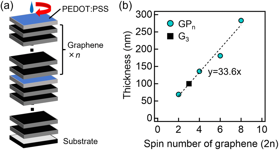 | ||
| Fig. 1 (a) Schematic diagram of the fabrication process of GPn and (b) the relationship between the number of graphene spin coating cycles (2n) and film thickness. In (b), the dashed line is a linear approximation line. | ||
The structures of these thin films were evaluated by X-ray diffraction (XRD) using an X-ray diffractometer (Rigaku, SmartLab), scanning electron microscopy (SEM)–energy dispersive X-ray spectroscopy (EDX) using a field emission SEM (Hitachi High-Technologies, S-5500), atomic force microscopy (AFM; Agilent Technologies), and Raman spectroscopy (Lambda Vision, Micro-RAM300/CHK-532-785-Gr1). For Raman spectroscopy, a 532 nm (30 mW) light source and a 50× objective lens were used. The electronic states were evaluated by X-ray photoelectron spectroscopy (XPS) with the characteristic X-ray source of Al Kα radiation (JEOL, JPS-9010).
σ was calculated from the sheet resistance measured by the van der Pauw method and film thickness measured using the cross-sectional SEM images of cut samples. S (=ΔV/ΔT) was calculated from the voltage difference (ΔV) and temperature difference (ΔT) measured with a self-made system and corrected with ZEM-3 (ADVANCE RIKO). Carrier concentration and mobility were measured by Hall effect measurements. Local electrical conductivity was measured by a 4-probe method with a probe distance of 100 μm.
3. Results and discussion
A cross-sectional SEM image of the GP3 sample is shown in Fig. S1 (ESI†). The upper and lower sides of the boundary indicated by the arrows are different from each other. The lower side is the glass substrate and the upper side is the thin film. The thickness of this thin film was approximately 180 nm. By plotting the film thickness of the prepared samples against the number of graphene spin-coating cycles (Fig. 1(b)), we found that the plots can be approximated by a straight line through the origin. The results indicate that almost the same amount of graphene is formed in each spin coating.The inset of Fig. 2(a) shows a photograph of the thin film surface in the GP3 sample, showing an agglomerated PEDOT:PSS area and an exposed graphene region on the thin film. The area around the agglomerated PEDOT:PSS was observed by surface SEM (Fig. 2(a)), showing that the agglomerated PEDOT:PSS area was less uneven, while the exposed graphene region was more uneven. Elemental mapping by SEM–EDX revealed that the agglomerated PEDOT:PSS contained a large amount of S (Fig. 2(b)), which is attributed to PEDOT:PSS. From the above results, PEDOT:PSS agglomerated on graphene layers.
 | ||
| Fig. 2 (a) SEM image and (b) EDX elemental mapping image (S) of the GP3 sample surface. The inset in (a) shows the surface image. Raman spectra of (c) PEDOT:PSS and (d) graphene region of the GP3 sample. AFM images of (e) PEDOT:PSS and (f) graphene region of the GP3 sample. | ||
The structures of the agglomerated PEDOT:PSS region and the exposed graphene region mentioned above were analyzed in more detail. Fig. 2(c) and (d) show the Raman spectra of the PEDOT:PSS and graphene regions of the GP3 sample, respectively. In the PEDOT:PSS region of the GP3 sample (Fig. 2(c)), a typical Raman band at 1449 cm−1 corresponding to the C![[double bond, length as m-dash]](https://www.rsc.org/images/entities/char_e001.gif) C symmetric stretching vibration of PEDOT was observed, where the peak position shifted to the higher wavenumber side compared to the peak position of 1447 cm−1 in P3 (Fig. S2, ESI†). This is due to the π–π interaction between graphene and PEDOT.36 Raman bands were also observed around 1520 cm−1 and 1600 cm−1 originating from the CC asymmetric and antisymmetric stretching vibrations of PEDOT,43 respectively, which are also observed in P3. On the other hand, in the graphene region (Fig. 2(d)), three typical Raman bands were observed: a G band at approximately 1578 cm−1 originating from the in-plane vibrational motion of sp2 hybridized carbon, and D and 2D bands at around 1346 cm−1 and 2683 cm−1, respectively, associated with overtones from the stretching motion of sp3 hybridized carbon.44,45 These Raman bands were also observed at similar wavenumbers in G3 (Fig. S2, ESI†).
C symmetric stretching vibration of PEDOT was observed, where the peak position shifted to the higher wavenumber side compared to the peak position of 1447 cm−1 in P3 (Fig. S2, ESI†). This is due to the π–π interaction between graphene and PEDOT.36 Raman bands were also observed around 1520 cm−1 and 1600 cm−1 originating from the CC asymmetric and antisymmetric stretching vibrations of PEDOT,43 respectively, which are also observed in P3. On the other hand, in the graphene region (Fig. 2(d)), three typical Raman bands were observed: a G band at approximately 1578 cm−1 originating from the in-plane vibrational motion of sp2 hybridized carbon, and D and 2D bands at around 1346 cm−1 and 2683 cm−1, respectively, associated with overtones from the stretching motion of sp3 hybridized carbon.44,45 These Raman bands were also observed at similar wavenumbers in G3 (Fig. S2, ESI†).
Fig. 2(e) and (f) show the AFM images of the PEDOT:PSS and graphene regions of the GP3 sample, respectively. The PEDOT:PSS region of the GP3 sample shows fibrous morphology, while P3 exhibits a random granular structure (Fig. S2, ESI†). This is because PEDOT:PSS typically has a coiled structure and random molecular arrangement, whereas due to the π–π interaction with graphene, PEDOT grows along the surface of graphene nanosheets, transforming the coiled structure into a linear one and its random molecular arrangement into an ordered arrangement.46 In the AFM images of both G3 and the graphene region of the GP3 sample, multiple sheet structures were observed.47 The RMS roughness of the graphene region of the GP3 sample was approximately 15 nm, which is comparable to that of G3 (∼20 nm).
Fig. 3(a) shows the XRD 2θ–ω scans of the GPn and G3 samples. For all samples, the glass substrate-derived peak at 21.7° and the 002 and 004 diffraction peaks of graphene at 26.4° and 54.5°, respectively, were observed. As shown in Fig. 3(a), the 002 diffraction peak intensity increased with the number of graphene spin-coating cycles. The plot of the 002 diffraction peak intensity, normalized by the glass substrate peak, against the number of graphene spin-coating cycles was approximated with a straight line through the origin (Fig. S3, ESI†). This indicates that the amount of graphene in the thin films increased proportionally with the number of spin coating cycles, which is consistent with the results shown in Fig. 1(b). Fig. 3(b) shows the full width at half maximum (FWHM) of the 002 diffraction peak of graphene. All GPn samples exhibited a reduced FWHM compared to G3. This suggests a smaller variation in the interlayer spacing of graphene, leading to high crystallinity, likely due to π–π interactions with PEDOT.44
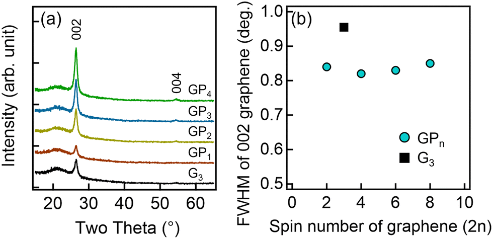 | ||
| Fig. 3 (a) XRD 2θ–ω scans for each thin film and (b) the dependence of the FWHM of the 002 graphene peak on the number of graphene spin coating cycles (2n). | ||
Fig. 4 shows the S (2p) XPS spectra of the PEDOT:PSS region in GP3 and P3 samples. Two peaks were observed at 166–170 eV and 162–166 eV attributed to sulfur in PSS and PEDOT, respectively. Notably, the PSS-derived peak intensity was lower for the GP3 sample compared to P3, indicating a reduction in the amount of PSS present at or near the surface detectable by XPS. This reduction can be caused by a reorganization within the PEDOT:PSS complex facilitated by the π–π interactions between graphene and PEDOT. The PEDOT-derived peak (162–166 eV) was fitted with two mixed Gaussian/Lorentzian functions, revealing peaks centered at 163.6 eV (neutral PEDOT) and 164.6 eV (oxidized PEDOT).48 These fitting results are summarized in Table 1. The GP3 sample exhibited a higher ratio of the neutral PEDOT component compared to P3, potentially due to the electron transfer from graphene to PEDOT:PSS. Furthermore, the PEDOT-derived peaks showed a slight shift towards lower binding energies in the GP3 sample, indicating the reduction of PEDOT, which is consistent with previous reports.49 Additionally, the peak corresponding to sulfur atoms in ionic PSS (component 3) decreased for the GP3 sample compared with P3. This is likely because PSS interacts less strongly with the PEDOT chains due to stronger PEDOT–graphene interactions.
 | ||
| Fig. 4 S (2p) XPS spectra of (a) GP3 and (b) P3 samples. The blue lines represent the sum of curves fitted with four components (dashed curves). | ||
| Sample | Component | Center (eV) | Area ratio (%) |
|---|---|---|---|
| GP3 | 1 | 163.6 | 18.8 |
| 2 | 164.6 | 44.4 | |
| 3 | 167.5 | 2.6 | |
| 4 | 168.3 | 34.2 | |
| P3 | 1 | 163.7 | 12.4 |
| 2 | 164.7 | 46.0 | |
| 3 | 167.8 | 18.9 | |
| 4 | 168.9 | 22.7 | |
The S, σ and S2σ values of the fabricated thin films plotted against the number of graphene spin-coating cycles are shown in Fig. 5(a)–(c), respectively. Fig. 5(a) shows that the GPn samples exhibited S values similar to those of graphene, except for GP1. In contrast, the σ values of the GPn samples were higher than those of G3. Notably, the GP3 sample exhibited a σ value approximately 1.7 times higher than that of G3. Additionally, GPn samples also exhibited higher S and σ than those of the PEDOT:PSS single-phase thin film (S ≈ 4 μV K−1, σ ≈ 46 S cm−1). Consequently, the S2σ value increased by about 1.6 times compared with G3, as shown in Fig. 5(c). To investigate the origin of this high S2σ, carrier concentration (p) and Hall mobility (μ) were measured by Hall effect measurements. As shown in Fig. 5(d), the GP3 sample exhibited higher p in contrast to its lower Hall mobility when compared to G3. This observation can be attributed to the electron transfer from graphene to PEDOT within the GP3 sample. This electron transfer is facilitated by the strong π–π interactions between the graphene and the conjugated polymer of PEDOT.36,39 However, a drop in σ was observed for the GP4 sample as shown in Fig. 5(b), which is due to a reduced effective interaction ratio between the PEDOT:PSS and the graphene layers with the increase of the number of graphene layers.
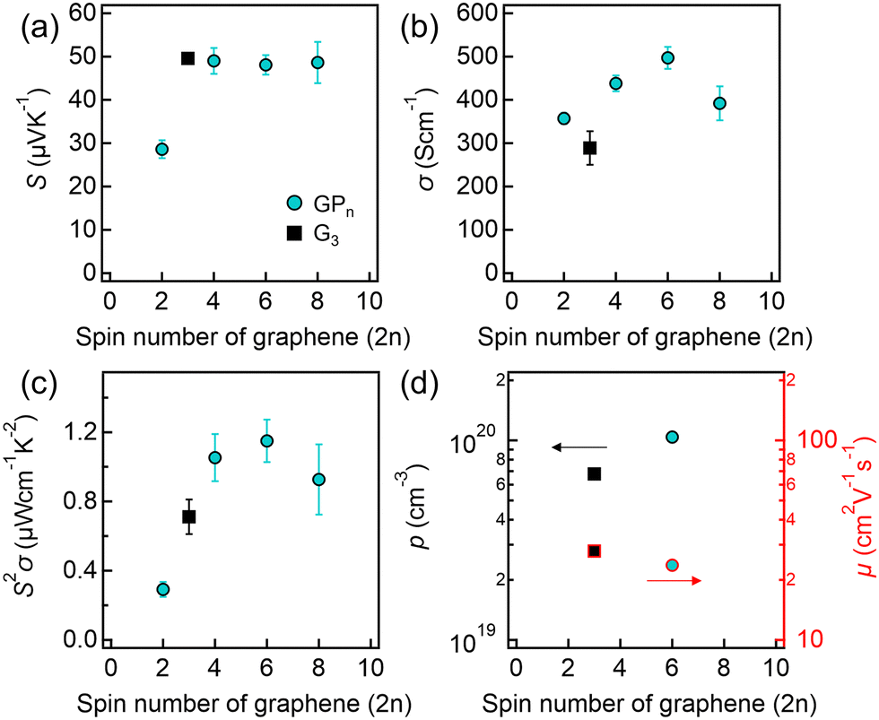 | ||
| Fig. 5 The dependences of (a) S, (b) σ, (c) S2σ, and (d) p (left axis) and μ (right axis) on the number of graphene spin coating cycles (2n) for each thin film. | ||
To investigate the carrier transport in detail, we measured the temperature dependence of the electrical properties of GP3 and G3. As shown in Fig. 6(a), the σ of both samples slightly increased as the temperature increased, indicating their semiconductor-like properties. In some previous reports, the carrier transport mechanism in reduced graphene oxide has been discussed using the Mott-variable range hopping (VRH) model and thermal activation.50 In the case of the three-dimensional Mott-VRH model, σ exhibits a T dependence given by σ ∝ exp(−(T0/T)−1/4), where T0 is the Mott characteristic temperature. However, the VRH model does not provide a good fit to the σ of GP3 and G3 because our samples show a nonlinear T−1/4 dependence of the logarithm of σ, as shown in Fig. 6(b).
 | ||
| Fig. 6 Temperature dependences of the electrical properties of GP3 and G3 samples: (a) σ vs. T, (b) σ vs. T−1/4, (c) p vs. T, and (d) μ vs. T. In (c), the dashed and dotted lines represent the fitting curves for GP3 and G3 samples, respectively. In (d), the dashed and dotted lines represent the temperature dependence of μ ∝ T−3/2 and μ ∝ T−1/2, respectively. | ||
Fig. 6(c) shows the T dependence of p. The p was fitted with the following equation based on a simple two-band model of bulk graphite:35,51
 | (1) |
The Hall mobilities of GP3 and G3 as a function of T are shown in Fig. 6(d). The μ values of both GP3 and G3 decreased as T increased. Considering that the dependence is similar for both samples, GP3 likely exhibits similar carrier scattering mechanisms to G3. This decrease in dependence might be considered to arise from acoustic phonon scattering. Although, in general, the large contribution of acoustic phonon scattering tends to be proportional to T−3/2 (dashed line), the experimental value exhibits a weaker dependence than T−1/2 (dotted line). Therefore, the carrier scattering mechanism must be extremely complicated because it might contain some other carrier scattering processes such as those caused by impurities, defects, interfaces, etc. Based on the above discussion, the high S2σ of GP3 originating from high σ is attributed to the enhancement of p by doping from PEDOT due to the π–π interactions.
Despite the agglomeration of PEDOT:PSS on graphene, the abovementioned thermoelectric properties were measured over the entire region. To understand the relationship between the electrical properties and the local structures, it is essential to measure local electrical properties. Here, the local electrical conductivity (σL) of the GP3 sample was measured using a 4-probe method. Fig. 7(a) shows the σL at various positions in the graphene region of the GP3 sample; in the PEDOT:PSS region, the contact resistance was too high to measure σL. Dotted and dashed lines indicate the average values of GP3 and G3, respectively. The σL of the graphene region in the GP3 sample was obviously higher than that of G3 in most areas. This indicates that the σL is high not only for graphene in contact with PEDOT:PSS, but also for the entire thin film, including the graphene region spatially distant from PEDOT:PSS. These results suggest that the local π–π interactions with PEDOT:PSS contribute to the electron transfer from graphene to PEDOT and the enhanced crystallinity of graphene throughout the thin film, resulting in high S2σ (Fig. 7(b)).
 | ||
| Fig. 7 (a) Local electrical conductivity (σL) in various graphene regions in GP3 and (b) schematic diagram of graphene doping from PEDOT:PSS via local π–π interactions. | ||
Finally, the S2σ of the GP3 sample fabricated in this study (1.2 μW cm−1 K2) was compared with those of previously reported PEDOT:PSS/graphene-based thin films (Table 2). The GP3 sample prepared in this study exhibited high S2σ comparable to a previous report (1.50 μW cm−1 K2) for PEDOT:PSS/rGO(20 wt%) prepared by the pad-dry-cure method.40 In this study, through the formation of agglomerated PEDOT:PSS, a relatively high S2σ was obtained despite the simplicity of the spin-coating method. Although the S2σ values of GPn samples were relatively low compared with other inorganic thermoelectric materials, we believe that our fabrication approach can contribute to the development of graphene-based thermoelectric materials.
| Sample | σ (S cm−1) | S (μV K−1) | S 2 σ (μW cm−1 K−2) | Ref. |
|---|---|---|---|---|
| This work | 497 | 48 | 1.2 | — |
| Graphene | 81 | 41 | 0.187 | 35 |
| PEDOT:PSS/graphene (70 wt%) | 96 | 17 | 0.029 | 41 |
| PEDOT:PSS/graphene (RTCVD) | 193 | 54 | 0.054 | 42 |
| PEDOT:PSS/rGO (2 wt%) | 32 | 59 | 0.11 | 38 |
| PEDOT:PSS/rGO (3 wt%) | 637 | 27 | 0.46 | 37 |
| PEDOT:PSS/rGO (16 wt%) | 51 | 61 | 0.050 | 36 |
| PEDOT:PSS/rGO (20 wt%) | 410 | 61 | 1.5 | 40 |
| PEDOT:PSS/GQD (13 wt%) | 72 | 15 | 0.015 | 39 |
4. Conclusions
In this study, we fabricated graphene/PEDOT:PSS thin films by a spin-coating method using graphene and PEDOT:PSS ink and evaluated their thermoelectric properties. In the thin films, PEDOT:PSS agglomerated on graphene thin films, which was observed by AFM and SEM–EDX. Raman spectroscopy and AFM analyses showed that the π–π interactions between graphene and PEDOT transform the coil structure into a linear structure and the random molecular arrangement into an ordered one. The π–π interactions stabilize the aromatic ring configuration and reduce variations in the graphene interlayer spacing. The S2σ of 1.2 μW cm−1 K−2 for the GP3 sample is 1.6 times higher than that of G3. The local π–π interactions with PEDOT:PSS contribute to the electron transfer from graphene to PEDOT and the enhanced crystallinity of graphene throughout the thin film, resulting in high S2σ.Author contributions
K. U.: data curation, investigation, and writing – original draft; S. S.: conceptualization, methodology, formal analysis, funding acquisition, visualization, writing – original draft, writing – review & editing; T. S.: investigation; A. A.: data curation; H. U.: writing – review & editing; H. T.: funding acquisition, supervision, writing – review & editing.Conflicts of interest
There are no conflicts to declare.Data availability
The data supporting this article have been included as part of the ESI.†Acknowledgements
This work was supported by the Grant-in-Aid for Early-Career Scientists (Grant Number 21K14479) from JSPS KAKENHI Japan and JST-ALCA-Next Japan (Grant Number JPMJAN24B3). We thank the Open Facility Center for Research, Ibaraki University for technical assistance. We thank Prof. H. Chang and K. Katayama at Chuo University for their support with XRD and Raman spectroscopy, respectively.References
- J. Mao, H. Zhu, Z. Ding, Z. Liu, G. A. Gamage, G. Chen and Z. Ren, Science, 2019, 365, 495–498 CrossRef CAS PubMed.
- I. J. Yoo, Y. Song, D. C. Lim, N. V. Myung, K. H. Lee, M. Oh, D. Lee, Y. D. Kim, S. Kim, Y. H. Choa, J. Y. Lee, K. H. Leea and J. H. Lim, J. Mater. Chem. A, 2013, 1, 5430–5435 RSC.
- F. Hao, P. Qiu, Y. Tang, S. Bai, T. Xing, H. S. Chu, Q. Zhang, P. Lu, T. Zhang, D. Ren, J. Chen, X. Shi and L. Chen, Energy Environ. Sci., 2016, 9, 3120–3127 RSC.
- A. Ayukawa, N. Kiridoshi, W. Yamamoto, A. Yasuhara, H. Udono and S. Sakane, Appl. Phys. Express, 2024, 17, 065501 CrossRef CAS.
- Y. Lu, Y. Ding, Y. Qiu, K. Cai, Q. Yao, H. Song, L. Tong, J. He and L. Chen, ACS Appl. Mater. Interfaces, 2019, 11, 12819–12829 CrossRef CAS PubMed.
- S. Sakane, T. Miura, K. Munakata, Y. Morikawa, S. Miwa, R. Yamanaka, T. Sugai, A. Ayukawa, H. Udono and H. Tanaka, Nanoscale Adv., 2024, 6, 3299–3305 RSC.
- S. Sakane, S. Miwa, T. Miura, K. Munakata, T. Ishibe, Y. Nakamura and H. Tanaka, ACS Omega, 2022, 7, 32101–32107 CrossRef CAS PubMed.
- J. Zhang, L. Song, A. Mamakhel, M. R. V. Jørgensen and B. B. Iversen, Chem. Mater., 2017, 29, 5371–5383 CrossRef CAS.
- Y. Pan, M. Yao, X. Hong, Y. Zhu, F. Fan, K. Imasato, Y. He, C. Hess, J. Fink, J. Yang, B. Büchner, C. Fu, G. J. Snyder and C. Felsera, Energy Environ. Sci., 2020, 13, 1717 RSC.
- X. Su, F. Fu, Y. Yan, G. Zheng, T. Liang, Q. Zhang, X. Cheng, D. Yang, H. Chi, X. Tang, Q. Zhang and C. Uher, Nat. Commun., 2014, 5, 4908 CrossRef CAS PubMed.
- Y. Ding, Y. Qiu, K. Cai, Q. Yao, S. Chen, L. Chen and J. He, Nat. Commun., 2019, 10, 841 CrossRef PubMed.
- C. Xiao, J. Xu, K. Li, J. Feng, J. Yang and Y. Xie, J. Am. Chem. Soc., 2012, 134, 4287–4293 CrossRef CAS PubMed.
- W. Mi, P. Qiu, T. Zhang, Y. Lv, X. Shi and L. Chen, Appl. Phys. Lett., 2014, 104, 133903 CrossRef.
- J. Tang, H. T. Wang, D. H. Lee, M. Fardy, Z. Huo, T. P. Russell and P. Yang, Nano Lett., 2010, 10, 4279–4283 CrossRef CAS PubMed.
- J. Tani and H. Kido, Physica B, 2005, 364, 218–224 CrossRef CAS.
- S. Sakane, T. Ishibe, T. Taniguchi, T. Hinakawa, R. Hosoda, K. Mizuta, M. M. Alam, K. Sawano and Y. Nakamura, Jpn. J. Appl. Phys., 2020, 59, SFFB01 CrossRef CAS.
- S. Sakane, T. Ishibe, T. Taniguchi, N. Naruse, Y. Mera, T. Fujita, M. M. Alam, K. Sawano, N. Mori and Y. Nakamura, Mater. Today Energy, 2019, 13, 56–63 CrossRef.
- J. L. Blackburn, A. J. Ferguson, C. Cho and J. C. Grunlan, Adv. Mater., 2018, 30, 1704386 CrossRef PubMed.
- Q. Y. Li, T. Feng, W. Okita, Y. Komori, H. Suzuki, T. Kato, T. Kaneko, T. Ikuta, X. Ruan and K. Takahashi, ACS Nano, 2019, 13, 9182–9189 CrossRef CAS PubMed.
- S. Sakane, T. Ishibe, Y. Yukawa and Y. Nakamura, Diamond Relat. Mater., 2023, 140, 110410 CrossRef CAS.
- X. Wang, H. Wang and B. Liu, Polymers, 2018, 10, 1196 CrossRef PubMed.
- Y. Xu, Z. Li and W. Duan, Small, 2014, 10(11), 2182–2199 CrossRef CAS PubMed.
- M. Sang, J. Shin, K. Kim and K. J. Yu, Nanomaterials, 2019, 9, 374 CrossRef CAS PubMed.
- P. Dollfus, V. H. Nguyen and J. Saint-Martin, J. Phys.: Condens. Matter, 2015, 27, 133204 CrossRef PubMed.
- A. Sharma, S. Sharma and S. Ajori, J. Mater. Sci., 2023, 58, 10222–10260 CrossRef CAS.
- A. H. C. Neto, F. Guinea, N. M. R. Peres, K. S. Novoselov and A. K. Geim, Rev. Mod. Phys., 2009, 81, 1 CrossRef.
- S. D. Sarma, S. Adam, E. H. Hwang and E. Rossi, Rev. Mod. Phys., 2011, 83, 2 Search PubMed.
- K. S. Novoselov, A. K. Geim, S. V. Morozov, D. Jiang, Y. Zhang, S. V. Dubonos, I. V. Grigorieva and A. A. Firsov, Science, 2004, 306, 666–669 CrossRef CAS PubMed.
- A. H. Reshak, S. A. Khan and S. Auluck, J. Mater. Chem. C, 2014, 2, 2346–2352 RSC.
- H. J. Goldsmid and J. W. Sharp, J. Electron. Mater., 1999, 28, 7 CrossRef.
- J. Duan, X. Wang, X. Lai, G. Li, K. Watanabe, T. Taniguchi, M. Zebarjadi and E. Y. Andrei, Proc. Natl. Acad. Sci. U. S. A., 2016, 113, 14272–14276 CrossRef CAS PubMed.
- Y. M. Zuev, W. Chang and P. Kim, Phys. Rev. Lett., 2009, 102, 96807 CrossRef PubMed.
- S. G. Nam, D. K. Ki and H. J. Lee, Phys. Rev. B: Condens. Matter Mater. Phys., 2010, 82, 245416 CrossRef.
- K. Kanahashi, M. Ishihara, M. Hasegawa, H. Ohta and T. Takenobu, npj 2D Mater. Appl., 2019, 3, 44 CrossRef.
- T. Juntunen, H. Jussila, M. Ruoho, S. Liu, G. Hu, T. Albrow-Owen, L. W. T. Ng, R. C. T. Howe, T. Hasan, Z. Sun and I. Tittonen, Adv. Funct. Mater., 2018, 28, 1800480 CrossRef.
- K. Xu, G. Chen and D. Qiu, J. Mater. Chem. A, 2013, 1, 12395–12399 RSC.
- D. Yoo, J. Kim and J. H. Kim, Nano Res., 2014, 7(5), 717–730 CrossRef CAS.
- G. H. Kim, D. H. Hwang and S. I. Woo, Phys. Chem. Chem. Phys., 2012, 14, 3530–3536 RSC.
- F. P. Du, N. N. Cao, Y. F. Zhang, P. Fu, Y. G. Wu, Z. D. Lin, R. Shi, A. Amini and C. Cheng, Sci. Rep., 2018, 8, 6441 CrossRef PubMed.
- N. A. Khoso, X. Jiao, X. G. Yu, S. Tian and J. Wang, RSC Adv., 2021, 11, 16675 RSC.
- J. Liu, G. Liu, J. Xu, C. Liu, W. Zhou, P. Liu, G. Nie, X. Duan and F. Jiang, ACS Appl. Energy Mater., 2020, 3, 6165–6171 CrossRef CAS.
- C. Park, D. Yoo, J. J. Lee, H. H. Choi and J. H. Kim, Org. Electron., 2016, 36, 166–170 CrossRef CAS.
- Y. Chen, J. Xu, Y. Yang, S. Li, W. Yang, T. Peng, X. L. Mao and Y. Zhao, J. Mater. Sci: Mater. Electron., 2015, 26, 8292–8300 CrossRef CAS.
- Y. Lu, Q. Yang, S. Wang, M. Liu, Y. Chen, Z. Zhao, A. R. Akbar, C. Xiong and G. H. Hu, Ionics, 2021, 27, 3615–3626 CrossRef CAS.
- N. Soin, S. S. Roy, C. O’Kane, J. A. D. McLaughlin, T. H. Limb and C. J. D. Hetherington, CrystEngComm, 2011, 13, 312–318 RSC.
- V. C. Tung, J. Kim, L. J. Cote and J. Huang, J. Am. Chem. Soc., 2011, 133, 9262–9265 CrossRef CAS PubMed.
- Z. M. Marković, M. D. Budimir, D. P. Kepić, I. D. Holclajtner-Antunović, M. T. Marinović-Cincović, M. D. Dramićanin, V. D. Spasojević, D. B. Peruško, Z. Špitalský, M. Mičušik, V. B. Pavlović and B. M. Todorović-Marković, RSC Adv., 2016, 6, 39275–39283 RSC.
- Y. Shirai, S. Takami, S. Lasmono, H. Iwai, T. Chikyow and Y. Wakayama, J. Polym. Sci., Part B: Polym. Phys., 2011, 49, 1762–1768 CrossRef CAS.
- J. H. Song, J. Jeong, J. Park, G. Park, I. Imae and J. Kwak, ACS Appl. Electron. Mater., 2024, 6, 6313–6321 CAS.
- Y. Wang, Y. Chen, S. D. Lacey, L. Xu, H. Xie, T. Li, V. A. Danner and L. Hu, Mater. Today, 2018, 21, 186–192 CrossRef CAS.
- K. Nagashio, T. Nishimura, K. Kita and A. Toriumi, Jpn. J. Appl. Phys., 2010, 49, 051304 CrossRef.
Footnotes |
| † Electronic supplementary information (ESI) available: Cross-sectional SEM images of GP3, Raman spectra and AFM images of graphene and PEDOT:PSS single-phase thin films are included. In addition, the intensity of the 002 XRD patterns of GPn and G3 samples is shown. See DOI: https://doi.org/10.1039/d5ma00454c |
| ‡ These authors contributed equally to this work. |
| This journal is © The Royal Society of Chemistry 2025 |