
 Open Access Article
 This Open Access Article is licensed under a
 Creative Commons Attribution 3.0 Unported Licence
GSAG:Ce scintillator: material optimization and intrinsic bottlenecks†
M.
Nikl
 *a,
J.
Pejchal
a,
J.
Ježek
b,
D.
Sedmidubský
b,
V.
Laguta
a,
V.
Babin
a,
A.
Beitlerová
a and
R.
Kučerková
a
*a,
J.
Pejchal
a,
J.
Ježek
b,
D.
Sedmidubský
b,
V.
Laguta
a,
V.
Babin
a,
A.
Beitlerová
a and
R.
Kučerková
a
aInstitute of Physics of the Czech Academy of Sciences, Cukrovarnicka 10/112, Prague, 16200, Czech Republic. E-mail: nikl@fzu.cz
bUniversity of Chemistry and Technology, Department of Inorganic Chemistry, Technická 5, Prague, 166 28, Czech Republic
First published on 13th May 2025
Abstract
Several Sc-admixed garnet single crystals of the general composition (Gd,Sc)3(Sc,Al)5O12:Ce and the well-established Gd3Ga2.7Al2.3O12:Ce (GGAG:Ce) one were grown using the micropulling down method. Their optical, luminescence and scintillation characteristics were measured and mutually compared to further optimize the former compositions and reveal the reason for their lower scintillation performance with respect to GGAG:Ce. Correlated experiments of time-resolved luminescence and scintillation spectroscopies further completed by thermoluminescence glow curve measurement and electron paramagnetic resonance (performed on Gd-free Sc-admixed garnets) indicate that Sc3+ is situated at the dodecahedral site of the garnet lattice as a dominant electron trap, creating a bottleneck in the scintillation mechanism of Sc-admixed garnets. This is mainly responsible for the degradation of scintillation efficiency in comparison with GGAG:Ce despite nearly the same effects of Sc and Ga in lowering the conduction band edge in these multicomponent garnets. Calculations of the electronic band structure confirm that the 3d energy levels of Sc3+ at the dodecahedral site are situated in the forbidden gap in Sc-admixed garnets.
1. Introduction
Single-crystal multicomponent garnet scintillators of the general formula (Gd,Y,Lu)3(Al,Ga)5O12:Ce were introduced in 2011,1,2 and Czochralski-grown crystals with the composition Gd3GaxAl5−xO12:Ce (x = 2.0–3.0), abbreviated as GGAG:Ce, reached the highest light yield of 58![[thin space (1/6-em)]](https://www.rsc.org/images/entities/char_2009.gif) 000 ph MeV−1 (x = 2.7) or best energy resolution of 4.2%@662 keV (x = 2.4).3 Luminescence and scintillation mechanisms, charge traps and different technological preparations have been studied in many laboratories worldwide.4–16 In analogy to simple YAG:Ce and LuAG:Ce garnets, in GGAG:Ce, Mg2+ and Ca2+ codoping was used to accelerate the scintillation response owing to the stabilization of Ce4+ at the expense of reduction of light yield.17–20 Despite such extended experimental efforts, electronic band structure calculations were absent for a long time and the first report appeared very recently,21 confirming that the down energy shift of the conduction band (CB) edge is mainly due to the Ga energy levels.
000 ph MeV−1 (x = 2.7) or best energy resolution of 4.2%@662 keV (x = 2.4).3 Luminescence and scintillation mechanisms, charge traps and different technological preparations have been studied in many laboratories worldwide.4–16 In analogy to simple YAG:Ce and LuAG:Ce garnets, in GGAG:Ce, Mg2+ and Ca2+ codoping was used to accelerate the scintillation response owing to the stabilization of Ce4+ at the expense of reduction of light yield.17–20 Despite such extended experimental efforts, electronic band structure calculations were absent for a long time and the first report appeared very recently,21 confirming that the down energy shift of the conduction band (CB) edge is mainly due to the Ga energy levels.
Despite its excellent scintillation performance, a GGAG-based single-crystal scintillator poses a problem from the viewpoint of production economy. Large crystals can be grown only using the Czochralski technique with a very expensive iridium crucible. This is because the presence of gallium excludes the use of a reduction atmosphere and cheaper molybdenum or tungsten crucibles.22,23 Thus, an alternative chemical composition was searched that provides a similar down energy shift of the CB bottom edge while enabling the use of cheaper crucibles. One such alternative could be Sc-admixed garnet, for which electronic band structure calculations have shown a substantial down energy shift of the CB bottom;24 moreover, it has been shown that the addition of an admixture of Sc into GGAG:Ce slightly decreases the ionization barrier for Ce3+ 5d1 state quenching.25 Kaurova et al.26 determined that the crystal growth via the Czochralski technique from the initial melt composition of Gd3Sc2Al3O12 results in a crystal composition of {Gd2.69Sc0.31}{Sc1.93Gd0.07}Al3O12, i.e., with pronounced occupation of the dodecahedral site by Sc and a minor occupation of the octahedral site by the Gd cation. The congruent composition for melt growth was determined to be Gd2.88Sc1.89Al3.23O12. Recently, the micropulling down (μ-PD) method was employed to prepare crystals of the Ce-doped congruent melting composition of Gd2.88Sc1.89Al3.23O12,27 and the Bridgman method was used to prepare crystals of the congruent and stoichiometric melt compositions,28 both from a molybdenum crucible under a reduction atmosphere. Their scintillation characteristics were reported to reach a maximum light yield of about 10000 ph MeV−1, which is about four times lower than that of μ-PD down grown crystals of GGAG:Ce in ref. 1. Very recently, a substantial light yield increase of up to 15000 ph MeV−1 was achieved in Gd3Sc2Al3O12:Ce (GSAG:Ce) crystals grown from a stoichiometric melt composition using the μ-PD method.29
This paper aims to search for further optimization of the scintillation characteristics of Gd-rich near-stoichiometric melt compositions of GSAG:Ce using the μ-PD crystal preparation method. By combining several optical and electron paramagnetic resonance (EPR) spectroscopies, we search for an explanation for its lower performance compared to that of the GGAG:Ce crystal prepared by applying the same technology. Furthermore, we perform quantum computation of the electronic band structure of various compositions of GSAG with different Sc concentrations to support the hypothesis of trapping migrating electrons in the transport stage of the scintillation mechanism derived from the experiment.
2. Experimental and calculation methods
2.1. Experimental methods
Crystals were grown by applying the μ-PD method; see the details in ref. 27 and 29 with radiofrequency inductive heating. The growth was performed using an Ir crucible with a die of 3 mm in diameter and a nozzle diameter of 0.5 mm under N2(4N) + 1% O2 atmosphere for the Gd3Ga2.7Al2.3O12:Ce crystal. The crucible was placed on an Ir afterheater with windows and an alumina pedestal. The hot zone around the crucible consisted of 3 layers of alumina shielding for thermal insulation. Other crystals were grown with a Mo crucible under an Ar + 5% H2 reducing atmosphere to further verify a more economical method of crystal growth from the melt.27–29 The gas flow was always kept at 0.5 L min−1. The pulling speed was 0.3 mm min−1. From crystal rods (see Fig. 1), plates of about 1 mm thick were cut and polished. Their chemical analysis was performed using the electron microanalyzer Jeol JX-8230 with energy-dispersive spectrometer Bruker QUANTAX 200 and using Esprit 2.2 software.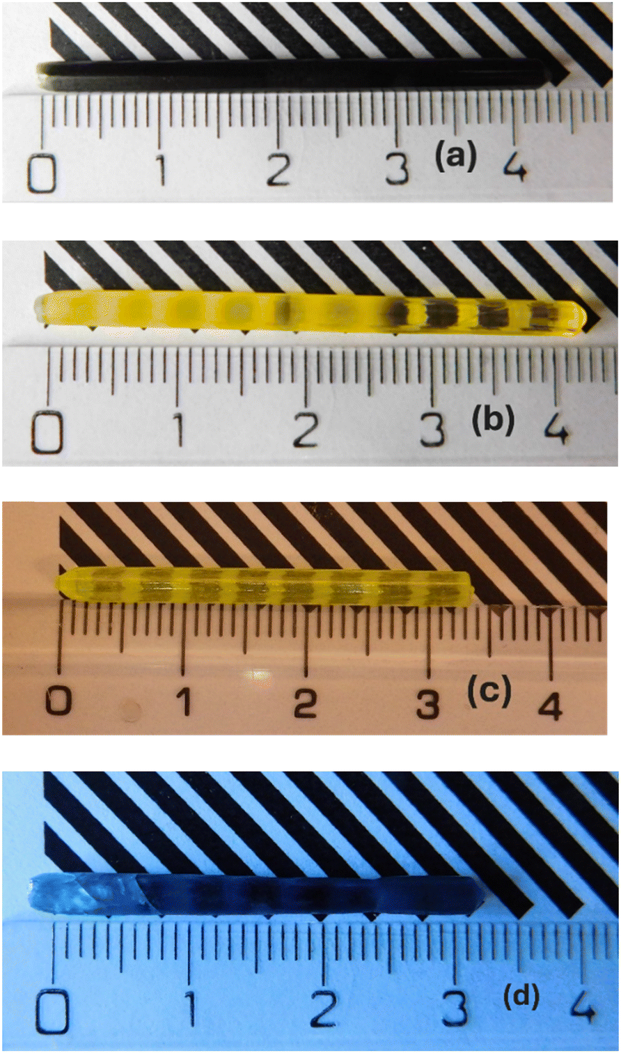 | ||
| Fig. 1 Photographs of some of the grown crystals: (a) Gd3Sc2 as grown; (b) Gd3Sc2 air-annealed (1200 °C/12 h); (c) Gd3Ga2.7 as grown; and (d) Y3Sc2Al3O12 as grown. | ||
Measurement of absorption spectra within 200–800 nm was performed by applying the UV/VIS/NIR spectrometer, Shimadzu 3101PC. The photoluminescence (PL) excitation (PLE) and emission spectra and PL decay curves were measured using custom-made spectrofluorometer 5000 M (Horiba Jobin Yvon) with excitation sources: (i) steady-state laser-driven xenon lamp (PL and PLE spectra, Energetiq EQ-99X LDLS–A Hamamatsu company) and (ii) nanosecond nanoLED pulsed light sources (IBH Scotland, fast PL decays). The detection part of 5000 M consists of a single-grating monochromator and photon counting detector TBX04 (IBH Scotland). The measured spectra were corrected for the spectral dependence of excitation energy (PLE) and the spectral dependence of detection sensitivity (PL). A convolution procedure was applied to the decay curves to determine true decay times using the SpectraSolve software package (Ames Photonics).
Radioluminescence (RL) spectra and afterglow were measured on 5000 M using an X-ray tube with a Mo anode (40 kV, 15 mA, Seifert GmbH) as an excitation source. Thermoluminescence (TSL) glow curves were measured at 5000 M in the range of 77–500 K using a Janis cryostat with a heating rate of 0. 1 K s−1 after excitation by applying the X-ray tube at 77 K. The scintillation light yield measurements were performed on the sample wrapped in reflective PTFE tape and optically coupled with silicon grease to a hybrid photomultiplier (HPMT) Photonis PP0475B with a built-in preamplifier. The excitation gamma source, radioisotope 137Cs (662 keV) and the amplifier shaping time of 1 μs were used in the measurement of pulse-height spectra. Scintillation decay curves were measured using the same 137Cs (662 keV) excitation and the Hamamatsu PMT U7600 and digital oscilloscope TDS3052 in the detection part. The convolution procedure was used similarly to that used for the PL decay evaluation.
The EPR spectra were measured using a commercial Bruker EMX plus spectrometer operating at the X-band (microwave frequency 9.25–9.5 GHz) within the temperature range of 10–290 K.
2.2. Electronic band structure calculations
They were performed using MedeA software30 with the implemented program VASP for electronic structure calculations. All calculations were based on the density functional theory (DFT) using the generalized gradient approximation (GGA)31 and the projector augmented wave (PAW)32 method. Specific pseudopotentials were set, Gd for Gd3+ and Sc_sv for Sc3+, as recommended by MedeA. In the self-consistent field method, the tetrahedron method with Blöchl corrections was used as the integration scheme over the first Brillouin zone. A typical k-mesh density of 0.25 Å−3 was applied. Owing to the strong correlation, we used LSDA + U with U = 7 eV for Gd-4f.33 The calculation was spin-polarized magnetic with a default planewave cutoff energy of 400 eV. As the initial atomic structure of Gd3Al5O12, we used a file from the ICSD database with a collection code of 23849.34 All other initial Sc-doped garnet structures were created by lowering symmetry from Ia-3d to Pcca and changing the relevant atomic sites to Sc so that the dopant was evenly distributed. In some cases, multiple configurations with the same Sc concentration were calculated, and only the structure with the lowest energy was used afterwards. Structural optimization was performed with the conjugate gradient update algorithm with a convergence of 0.03 eV Å−1. We optimized all atomic sites and lattice parameters so that the Pcca symmetry and lattice parameters were retained. All optimizations converged after circa 15 iterations because the initial system was very close to the optimized state. For the optimized structures, we calculated the density of states, where only the tetrahedron method was applied.3. Results and discussion
3.1. Crystal growth
Using micropulling down technology, the crystals with initial melt composition of Gd3Sc2Al3O12:Ce0.3 at% (further denoted as Gd3Sc2), Gd3.03Sc2Al3O12:Ce0.3 at% (further denoted as Gd3.03Sc2) and Gd3.09Sc2Al3O12:Ce0.3 at% (further denoted as Gd3.09Sc2) were grown using a molybdenum crucible and Ar + H2 reduction atmosphere. For comparison purposes, we grew Gd3Ga2.7Al2.3O12:Ce0.3 at% crystal (further denoted as Gd3Ga2.7) using the same technology but with an Ir crucible and N2 + 1% O2 atmosphere. Photographs of selected crystals are illustrated in Fig. 1, and the composition measured at the sample plates is in Table 1. Crystals grown from molybdenum crucible were annealed at 1200 °C/12 h in the air to remove their dark color due to unspecified color centres (see Fig. 1). To enable EPR measurements requiring Gd-free compositions, we grew isostructural Gd-free crystals with melt compositions of Y3Sc2Al3O12 and Y2.89Sc1.16Al3.95O12, see also Fig. 1. The Gd-free crystals showed cracks in the initial part owing to a non-optimized temperature profile beneath the crucible in the crystal growth process.| Sample | Gd2O3 | Sc2O3 | Al2O3 | Ce2O3 |
|---|---|---|---|---|
| Gd3Sc2 | 3.001 | 1.987 | 3.002 | 0.010 |
| Gd3.03Sc2 | 3.032 | 2.007 | 2.953 | 0.008 |
| Gd3.09Sc2 | 3.073 | 2.076 | 2.843 | 0.008 |
| Gd3Ga2.7 | 3.050 | 2.700 (Ga2O3) | 2.200 | 0.008 |
3.2. Absorption spectra
As depicted in Fig. 2, the absorption spectra of Gd3Sc2 and Gd3Ga2.7 samples are shown. Different relative amplitudes of 4f–5d1 (440–450 nm), 4f–5d2 (340 nm) and 4f–5d3,4,5 (220–240 nm) are noticed when both samples are compared, while their positions are almost the same. Long wavelength shift of 4f–5d1 absorption band by about 8 nm in Gd3Sc2 indicates a slightly enhanced crystal field at the dodecahedral site when the Ga cation is changed to the Sc one. As expected, the positions and amplitudes of the Gd3+ 4f–4f transitions at 275 nm and 305–312 nm are the same in both samples. Most importantly, the position of the host band edge onset around 210–215 nm is almost the same in both samples, which evidences very similar positioning of the conduction band bottom edge.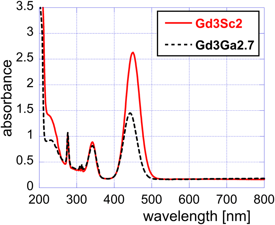 | ||
| Fig. 2 Absorption spectra of Gd3Sc2 and Gd3Ga2.7 samples annealed at 1200 °C for 12 hours in air. | ||
The absorption spectra of the Gd3.03Sc2 and Gd3.09Sc2 samples in Fig. S1 (ESI†) are closely similar to that of Gd3Sc2 in Fig. 2.
3.3. Radioluminescence spectra
The RL spectra maxima of the Gd3Sc2, Gd3.03Sc2 and Gd3.09Sc2 samples (cca 550 nm) have long wavelength shifted with respect to the Gd3Ga2.7 one (530 nm), as illustrated in Fig. 3, which is consistent with the 4f–5d1 band shift in the absorption spectra depicted in Fig. 2. The RL amplitudes of the Gd3Sc2, Gd3.03Sc2 and Gd3.09Sc2 samples are similar, about 2.5 times that of BGO, while that of Gd3Ga2.7 is much higher, about 8.3 times that of BGO, which indicates a much higher scintillation efficiency of the Gd3Ga2.7 sample. | ||
| Fig. 3 RL spectra of the sample set in absolute comparison with the BGO standard scintillator. | ||
3.4. Scintillation decays and afterglow
The scintillation decay of the Gd3Sc2 sample in Fig. 4 shows an even faster dominant decay component with a decay time of 90.1 ns 90.1 ns compared to the 111 ns of the Gd3Ga2.7, but its timing performance measured by the 1/e decay time (DT) is degraded by the presence of an intense rise component with a rise time of 70.6 ns. Even longer 1/e DT's is obtained for Gd3.03Sc2 (274 ns) and Gd3.09Sc2 (266 ns) samples (see Fig. S2a and b (ESI†) and Table 2). Such intensely rising components were also evidenced in GSAG:Ce crystals prepared by applying the Bridgman method.28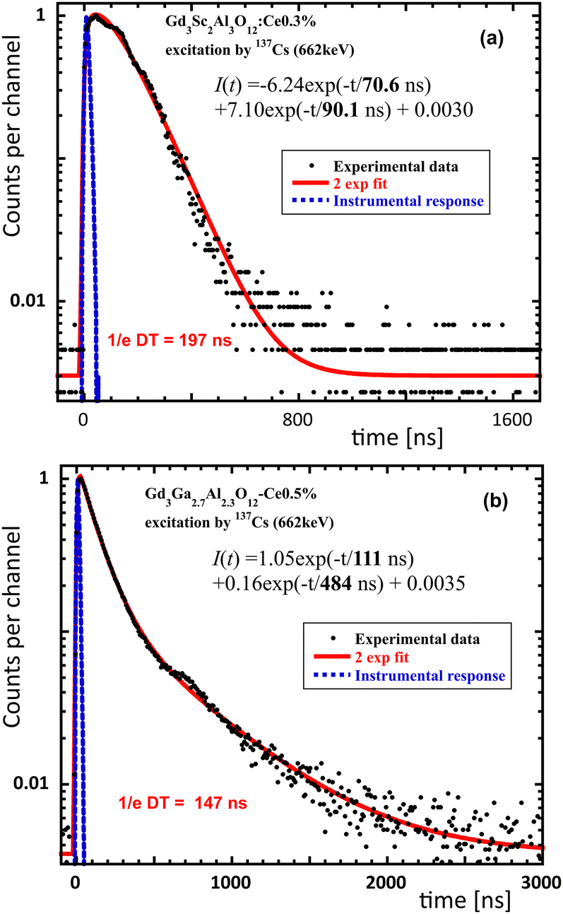 | ||
| Fig. 4 Scintillation decays of (a) Gd3Sc2 and (b) Gd3Ga2.7, spectrally unresolved. The red line is the convolution of the instrumental response and function I(t) in the figure. | ||
| Sample | LY (ph MeV−1) annealed 1200 °C | LY (ph MeV−1) annealed 1200 & 1500 °C | 1/e decay time (ns) |
|---|---|---|---|
| Gd3Sc2 | 15080 |
16810 |
197 |
| Gd3.03Sc2 | 15060 |
17320 |
274 |
| Gd3.09Sc2 | 14030 |
15360 |
266 |
| Gd3Ga2.7 | 42760 |
n/a | 147 |
| BGO standard | 7850 (no annealing) | n/a | n/a |
The afterglow of all the samples in Fig. 5 is very competitive, within 0.02–0.03% at 10 ms after the X-ray cut-off, and that of the BGO standard is about 0.01%.
 | ||
| Fig. 5 Afterglow of all samples and the BGO standard. Curves are horizontally shifted for clarity, and the X-ray cut-off is indicated. | ||
3.5. Photoluminescence decays
To determine the influence of the deteriorating processes of any kind acting at the excited state of the Ce3+ luminescence center at room temperature, PL decays are the best probe. As illustrated in Fig. 6, the PL decays of Gd3Sc2 and Gd3Ga2.7 are shown for direct comparison. The PL decays of Gd3.03Sc2 and Gd3.09Sc2 are very similar to that of Gd3Sc2, as shown in Fig. S3a and b (ESI†). | ||
| Fig. 6 PL decays at RT of (a) Gd3Sc2 and (b) Gd3Ga2.7 samples. Exc = 452 nm, Em = 550 nm (a) and 530 nm (b). The red solid line is the convolution of the instrumental response and the function I(t) in the figure. | ||
Considering the low temperature lifetimes of the 530 nm band in GGAG:Ce1 and the 550 nm band in GSAG:Ce27 around 55–60 ns and 65 ns, respectively, and the significantly faster decay of the Gd3Sc2 sample depicted in Fig. 6b, it can be concluded that the Ce3+ center in Gd3Sc2 is significantly quenched compared to the Gd3Ga2.7 host. The PLQY at RT, estimated from the mentioned decay times in the Gd3Sc2 sample, is about 49/65 = 0.75. The quenching process is due to the 5d1 excited state ionization.1,27 However, the difference in the range of a few tens of percent cannot explain the huge difference in scintillation efficiency derived from the RL spectra depicted in Fig. 3. It is also worth noting that the PL decays are faster compared to the scintillation ones in Fig. 4 and Fig. S2a and b (ESI†), indicating additional delay/slowdown in the transfer stage of the scintillation mechanism.
3.6. Scintillation light yield
Scintillation light yield (LY) was measured with a 1 μs shaping time so that only fast enough scintillation light generated within this time window is registered here. As illustrated in Table 2, the values are summarized in ph MeV−1 units. Furthermore, the 2nd annealing in the air at 1500 °C/12 h was applied, which has shown a clear positive effect on all the Gd3Sc2, Gd3.03Sc2 and Gd3.09Sc2 samples. We applied yet another 3rd annealing at 1550 °C/12 h, which did not show any effect.From all the data presented in Section 3.2–3.6, it can be observed that despite the similar decrease in CB bottom edge due to the Ga or Sc admixture in the garnet composition, which should deactivate some parts of the electron traps, the scintillation efficiency and the light yield are considerably lower in all the Sc-containing garnets compared to Gd3Ga2.7 prepared by applying the same μ-PD method. Somewhat more severe quenching observed in PL decays of Sc-containing garnets cannot explain such a huge difference, so the reason must involve a different mechanism of charge capture and nonradiative recombination processes in materials with Sc or Ga cations. This is discussed in Section 3.7.
3.7. Electron traps in Sc-containing garnets
In the Ce3+-doped scintillators, most holes generated in the conversion stage of the scintillation mechanism are immediately and effectively captured by the Ce3+ ions owing to their high concentration and high ability for hole capture, becoming temporarily Ce4+. The electrons, however, can be captured during the transfer stage of the scintillation mechanism at various electron traps, which delays their transport towards temporary Ce4+ to radiatively recombine here and yield scintillation photons. Thus, the study of electron traps in Ce-doped scintillation materials is of the utmost importance in revealing eventual bottlenecks and the limits of their performance.35For the study of charge carrier capture in the lattice, the TSL and EPR experiments can be effectively correlated to reveal the acting traps and understand their nature. In Gd-based compounds, however, EPR cannot be used as a superstrong EPR signal from paramagnetic Gd3+ obscures signals from any other centers. Moreover, spins from any defect are exchange-coupled to Gd3+ spins, creating a very non-informative broad EPR signal. Thus, we prepared structurally equivalent Y3Sc2Al3O12 and Y2.89Sc1.16Al3.95O12 single crystals for the EPR study of electron traps.
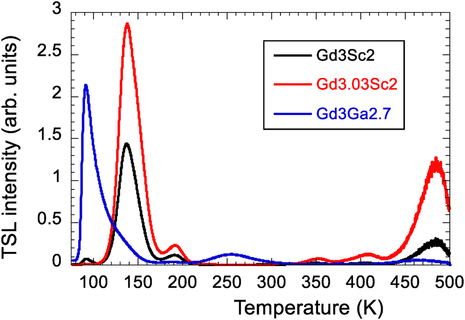 | ||
| Fig. 7 TSL glow curves of selected samples corrected for the temperature dependence of PL spectra. | ||
 | ||
| Fig. 8 Absorption spectra of Y3Sc2Al3O12 as grown and annealed in air at 1200 °C/12 h. | ||
The EPR experiment confirmed the presence of defects containing Sc2+ ions in the as-grown crystal (Fig. 9, panel a). The spectrum in the as-grown sample is nearly isotropic (it is almost the same in the crystal and in the ground crystal) and is described by a g-factor of 1.980. It also shows a well-resolved hyperfine (HF) structure with eight equidistant lines that clearly originate from the 45Sc isotope (nuclear spin I = 7/2, natural abundance = 100%, and hyperfine splitting A = 54 × 10−4 cm−1). Annealing the crystal in the air leads to the disappearance of the Sc2+ spectrum (Fig. 9, panel b). These facts indicate that the center is of an F+-type (an electron trapped at an oxygen vacancy), as observed previously in YAG38 and LuAG crystals.39 In contrast to the F+ center in YAG or LuAG, an electron in the Y2Sc2Al3O12 is trapped at an oxygen vacancy in the vicinity of the Sc ion, as the electron density is markedly localized at the Sc ion (it follows from the observed hyperfine interaction with the 45Sc nuclear spin). The center can thus be designed for the Sc2+-VO center. All these experimental facts suggest that the coloration of the as-grown Y3Sc2Al3O12 crystal is surely related to the presence of Sc2+-VO centers, which is consistent with the conclusion made in ref. 37 for the undoped GSAG crystal.
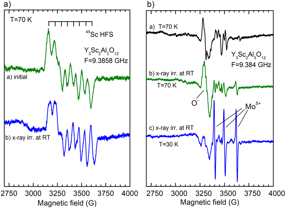 | ||
| Fig. 9 Panel (a): EPR spectra in the Y3Sc2Al3O12 as-grown crystal; panel (b): EPR spectra in the Y3Sc2Al3O12 crystal annealed in air. Panel (a) presents EPR spectra measured in the crystal before X-ray irradiation (a) and in the crystal after X-ray irradiation at room temperature (b). The as-grown crystal shows an HF structure from the 45Sc isotope (eight equidistant lines). Panel (b) presents EPR spectra measured in the crystal annealed in the air before X-ray irradiation (a) and after X-ray irradiation (b and c). In the annealed crystal, the spectrum with the 45Sc HF structure is absent. Instead, the spectra of the O− center and Mo5+ ions appear. | ||
X-ray irradiation of the as-grown crystal does not create any additional EPR-active defects (Fig. 9, panel a, spectrum b). In contrast, the X-ray irradiation of air-annealed crystal creates O− paramagnetic centers (Fig. 9, panel b, spectrum b). This is the most common defect created by X-ray or γ-ray irradiation in garnet crystals.38 The O− EPR spectrum is unusually strong in intensity in the Y2.89Sc1.16Al3.95O12 melt composition (Fig. 10), suggesting that O− centers can be created in the vicinity of Sc ions at antisite position by trapping a hole by an oxygen lattice ion (such Sc ion makes strong perturbation for host oxygen ion, thus increasing the thermal stability of the O− center). Besides, the EPR spectrum of Mo5+ ions appears as well (Fig. 9, panel b, spectrum c). The Mo ions come from the Mo crucible and, under irradiation, recharge to the Mo5+ valence state to compensate for (together with O− ions) the excess negative charge in the lattice introduced by annealing in the air. Their concentration is estimated in the range of 0.1–1 at. ppm.
 | ||
| Fig. 10 O− EPR spectrum measured in the X-ray irradiated (at 77 K) grinded Y2.89Sc1.16Al3.95O12 crystal. All spectra are measured at 75 K. | ||
4. Electronic band structure calculations
Following,26 we worked with the assumption that Sc can occupy only the octahedral and dodecahedral sites. We proposed and optimized superstructures with six different concentrations of evenly distributed Sc atoms on the octahedral and dodecahedral sites in Gd3Al5O12 (GAG). With the optimized structures, we calculated the density of states and compared the energies of the bands, revealing primarily the character of the Sc valence states.As depicted in Fig. 11 and 12, the density of states plots are presented, focusing on the valence and conduction bands. Partial DOS (PDOS) projected on the respective valence states of elements was multiplied by the number of equivalent Wyckoff positions to obtain the total PDOS per formula unit, i.e. for all equivalent atoms.
 | ||
| Fig. 11 Density of states of structures without Sc in the octahedral site. Total DOS is black, Gd-4f is purple, Gd-5d is blue, Sc-3d on the dodecahedral site is green and O-2p is red. | ||
 | ||
| Fig. 12 Density of states of structures with Sc in both the octahedral and dodecahedral sites. Total DOS is black, Gd-4f is purple, Gd-5d is blue, Sc-3d on the dodecahedral site is green, Sc-3d on the octahedral site is yellow and O-2p is red. The Gd-5d band is hidden under the Sc-3d line. | ||
By calculating the DOS of the optimized structures of these Sc-admixed garnets, our results support the hypothesis drawn from the experiments, which demonstrates that the energies of the Sc3+-3d states in dodecahedral sites are located in the bandgap under the conduction band minimum, creating electron traps. The shift of the Sc-3d levels deeper into the gap is imposed by weaker covalent bonding, making the Sc-3d orbitals less antibonding due to weaker metal–ligand orbital overlap, despite a slightly stronger crystal field of the dodecahedral position with a higher coordination number.
5. Conclusions
Using micropulling down technology, single crystals of the starting melt composition Gd3Sc2Al3O12:Ce0.3 at%, Gd3.03Sc2Al3O12:Ce0.3 at%, and Gd3.09Sc2Al3O12:Ce0.3 at% were grown from a molybdenum crucible under a reduction atmosphere and Gd3Ga2.7Al2.3O12:Ce0.3 at% crystal from an Ir crucible under N2 + 1%O2 atmosphere. Crystal compositions were determined by applying an electron microprobe method. Annealing in the air at 1200 °C/12 h and 1500 0C/12 h was applied to the former group in two steps. The optical, luminescence and scintillation characteristics were measured for all of them to compare characteristics between the Sc-admixed and Ga-admixed crystals. The highest light yield was obtained in the doubly air annealed Gd3.03Sc2Al3O12:Ce0.3 at% crystals, providing a value of 17320 ph MeV−1, while that of Gd3Ga2.7Al2.3O12:Ce0.3% was 42760 ph MeV−1. Similarly, the amplitudes of their RL spectra compared to BGO were about 2.5 and 8.3, respectively. Furthermore, the Y3Sc2Al3O12 and Y2.89Sc1.16Al3.95O12 crystals were grown similarly to the Sc-admixed Gd-based ones and used for the EPR experiment to determine the nature of the electron traps. Electronic band structure calculations were performed for several compositions of the Sc-admixed garnet structure.
The significantly lower scintillation performance of the Sc-admixed garnets compared with the well-established Gd3Ga2.7Al2.3O12:Ce0.3 at% multicomponent garnets is explained by the antisite Sc3+ ion at the dodecahedral position of Gd3+(ScGd) in the garnet structure, which forms a deep electron trap. Electron capture at Sc3+ was proved by EPR, creating the Sc2+-VO center in the as-grown Y3Sc2Al3O12 crystal, which is also responsible for absorption bands in the range of 600–900 nm. This center and its related absorption disappear after annealing in air at 1200 °C/12 h. An anomalously high concentration of O− centers is revealed in Y2.89Sc1.16Al3.95O12 annealed in air at 1200 °C/12 h by EPR compared to Y3Al5O12 or Lu3Al5O12 crystals. Such centers require charge compensation in the lattice, and the Sc2+ is the most probable option. Intense TSL glow curves above room temperature evidence the existence of deep electron traps in the Ce-doped Sc-admixed crystals, and the electronic band structure calculations show that the Sc3+ at the dodecahedral position forms the energy levels within the forbidden gap below the bottom of the conduction band, which provides further support for such an explanation.
Thus, despite a similar downshift of conduction band bottom edge in the Gd3Sc2Al3O12 and Gd3Ga2.7Al2.3O12 structures, which should deactivate shallow electron traps, such a new deep electron trap in the Sc-admixed garnets, the formation of which is an intrinsic feature in the crystal grown from the melt, significantly deteriorates its scintillation performance for the overall scintillation efficiency and light yield characteristics.
Author contributions
Martin Nikl: conceptualization, data curation, investigation, validation, visualization, writing – original draft, writing – review & editing, funding acquisition, supervision. Jan Pejchal: crystal growth, writing – review & editing. Jakub Ježek and David Sedmidubský: theoretical calculations, writing – original draft, writing – review & editing. Kučerková Romana: data curation, formal analysis, investigation, visualization. Valentin Laguta: EPR experiment, data curation, formal analysis, investigation, visualization, writing – original draft writing – review & editing. Vladimir Babin: TSL experiment, data curation, formal analysis, investigation, visualization, writing – review & editing. Alena Beitlerová, Romana Kučerková: data curation, formal analysis, investigation.Data availability
The data related to figures are available upon request from the corresponding author.Conflicts of interest
There are no conflicts of interest to declare.Acknowledgements
This research was supported by Czech Science Foundation project no. 21-17731S and by OP JAC financed by ESIF and MEYS (project LASCIMAT–CZ.02.01.01/00/23_020/0008525). Computational resources were provided by the e-INFRA CZ project (project ID no.: 90254), supported by the Ministry of Education, Youth and Sports of the Czech Republic. We acknowledge the help of K. Jurek and M. Jarošová, who performed chemical analysis of the samples.References
- K. Kamada, T. Yanagida, T. Endo, K. Tsutumi, Y. Fujimoto, A. Fukabori, A. Yoshikawa, J. Pejchal and M. Nikl, Cryst. Growth Des., 2011, 11, 4484–4490 CrossRef CAS.
- K. Kamada, T. Yanagida, J. Pejchal, M. Nikl, T. Endo, K. Tsutumi, Y. Fujimoto, A. Fukabori and A. Yoshikawa, J. Phys. D: Appl. Phys., 2011, 44, 505104 CrossRef.
- K. Kamada, S. Kurosawa, P. Prusa, M. Nikl, V. V. Kochurikhin, T. Endo, K. Tsutumi, H. Sato, Y. Yokota, K. Sugiyama and A. Yoshikawa, Opt. Mater., 2014, 36, 1942–1945 CrossRef CAS.
- O. Sidletskiy, V. Kononets, K. Lebbou, S. Neicheva, O. Voloshina, V. Bondar, V. Baumer, K. Belikov, A. Gektin and B. Grinyov, Mater. Res. Bull., 2012, 47, 3249–3252 CrossRef CAS.
- P. Dorenbos, J. Lumin., 2013, 134, 310–318 CrossRef CAS.
- J. M. Ogiegło, A. Katelnikovas, A. Zych, T. Justel, A. Meijerink and C. R. Ronda, J. Phys. Chem. A, 2013, 117, 2479–2484 CrossRef PubMed.
- K. Brylew, W. Drozdowski, A. J. Wojtowicz, K. Kamada and A. Yoshikawa, J. Lumin., 2014, 154, 452–457 CrossRef CAS.
- V. Laguta, Y. Zorenko, V. Gorbenko, A. Iskaliyeva, Y. Zagorodniy, O. Sidletskiy, P. Bilski, A. Twardak and M. Nikl, J. Phys. Chem. C, 2016, 120, 24400–24408 CrossRef CAS.
- I. I. Vrubel, R. G. Polozkov, I. A. Shelykh, V. M. Khanin, P. A. Rodnyi and C. R. Ronda, Cryst. Growth Des., 2017, 17, 1863–1869 CrossRef CAS.
- C. Wang, D. Ding, Y. Wu, H. Li, X. Chen, J. Shi, Q. Wang, L. Ye and G. Ren, Appl. Phys. A, 2017, 123, 1–6 CrossRef.
- M. Kitaura, H. Zen, K. Kamada, S. Kurosawa, S. Watanabe, A. Ohnishi and K. Hara, Appl. Phys. Lett., 2018, 112, 031112 CrossRef.
- V. Kochurikhin, K. Kamada, K. J. Kim, M. Ivanov, L. Gushchina, Y. Shoji, M. Yoshino and A. Yoshikawa, J. Cryst. Grow., 2020, 531, 125384 CrossRef CAS.
- M. Li, M. Meng, J. Chen, Y. Sun, G. Cheng, L. Chen, S. Zhao, B. Wan, H. Feng, G. Ren and D. Ding, Phys. Status Solidi B, 2021, 258, 2000603 CrossRef CAS.
- S. Nargelas, Y. Talochka, A. Vaitkevičius, G. Dosovitskiy, O. Buzanov, A. Vasil'ev, T. Malinauskas, M. Korzhik and G. Tamulaitis, J. Lumin., 2022, 242, 118590 CrossRef CAS.
- T. Wu, et al. , Cryst. Growth Des., 2022, 22, 180–190 CrossRef CAS.
- A. Yoshikawa, V. V. Kochurikhin, M. Yoshino, R. Murakami, T. Tomida, I. Takahashi, K. Kamada, Y. Shoji, H. Sato, R. Kucerkova, A. Beitlerova and M. Nikl, Cryst. Growth Des., 2023, 23, 2048–2054 CrossRef.
- Y. Wu, F. Meng, Q. Li, M. Koschan and C. L. Melcher, Phys. Rev. Appl., 2014, 2, 044009 CrossRef CAS.
- K. Kamada, M. Nikl, S. Kurosawa, A. Beitlerova, A. Nagura, Y. Shoji, J. Pejchal, Y. Ohashi, Y. Yokota and A. Yoshikawa, Opt. Mater., 2015, 41, 63–66 CrossRef CAS.
- G. Tamulatis, G. Dosovitskiy, A. Gola, M. Korjik, A. Mazzi, S. Nargelas, P. Sokolov and A. Vaitkevičius, J. Appl. Phys., 2018, 124, 215907 CrossRef.
- M. Korzhik, V. Alenkov, O. Buzanov, G. Dosovitskiy, A. Fedorov, D. Kozlov, V. Mechinsky, S. Nargelas, G. Tamulaitis and A. Vaitkevičius, CrystEngComm, 2020, 22, 2502–2506 RSC.
- F. Zajíc, V. Jarý, J. Pospíšil, P. Boháček, Z. Umar, M. Piasecki, M. G. Brik, R. Kučerková, A. Beitlerová and M. Nikl, Mater. Adv., 2024, 6, 777–787 RSC.
- O. Sidletskiy, P. Arhipov, S. Tkachenko, Ia Gerasymov, D. Kurtsev, V. Jarý, R. Kučerková, M. Nikl, K. Lebbou and E. Auffray, Engineering of Scintillation Materials and Radiation Technologies, ISMART, in Springer Proceedings in Physics, ed. M. Korzhik, A. Gektin, 2018, vol. 227, Springer, Cham Search PubMed.
- K. Kamada, et al. , J. Cryst. Grow., 2020, 535, 125510 CrossRef CAS.
- Y.-N. Xu, W. Y. Ching and B. K. Brickeen, Phys. Rev. B: Condens. Matter Mater. Phys., 2000, 61, 1817–1824 CrossRef CAS.
- D. Spassky, et al. , CrystEngComm, 2020, 22, 2621–2631 RSC.
- I. A. Kaurova, E. N. Domoroshchina, G. M. Kuz’micheva and V. B. Rybakov, J. Cryst. Grow., 2017, 468, 452–456 CrossRef CAS.
- O. Zapadlík, J. Pejchal, R. Kučerková, A. Beitlerová and M. Nikl, Cryst. Growth Des., 2021, 21, 7139–7149 CrossRef.
- K. L. Hovhannesyan, M. V. Derdzyan, G. Badalyan, G. Kharatyan, J. Pejchal, M. Nikl, C. Dujardin and A. G. Petrosyan, CrystEngComm, 2024, 26, 4812–4819 RSC.
- O. Zapadlík, J. Pejchal, V. Babin, V. Jarý, V. Vaněček, R. Kučerková, K. Jurek, A. Beitlerová and M. Nikl, RSC Adv., 2025, 15, 2140–2151 RSC.
- G. Kresse and J. Furthmüller, Phys. Rev. B: Condens. Matter Mater. Phys., 1996, 54, 11169–11186 CrossRef CAS PubMed.
- J. P. Perdew, K. Burke and M. Ernzerhof, Phys. Rev. Lett., 1996, 77, 3865 CrossRef CAS PubMed.
- G. Kresse and D. Joubert, Phys. Rev. B: Condens. Matter Mater. Phys., 1999, 59, 1758–1775 CrossRef CAS.
- L. Dudarev, S. Y. Savrasov, C. J. Humphreys and A. P. Sutton, Phys. Rev. B: Condens. Matter Mater. Phys., 1998, 57, 1505 CrossRef.
- F. Euler and J. A. Bruce, Acta Crystallogr., 1965, 19, 971–978 CrossRef CAS.
- M. Nikl, V. V. Laguta and A. Vedda, Phys. Status Solidi B, 2008, 245, 1701–1722 CrossRef CAS.
- F. Moretti, G. Patton, A. Belsky, M. Fasoli, A. Vedda, M. Trevisani, M. Bettinelli and C. Dujardin, J. Phys. Chem. C, 2014, 118, 9670–9676 CrossRef CAS.
- K. L. Hovhannesyan, M. V. Derdzyan, I. A. Ghambaryan, T. I. Butaeva, C. Dujardin and A. G. Petrosyan, Phys. Status Solidi A, 2023, 220, 2300386 CrossRef CAS.
- V. Laguta, M. Buryi, P. Arhipov, O. Sidletskiy, O. Laguta, M. G. Brik and M. Nikl, Phys. Rev. B, 2020, 101, 024106 CrossRef CAS.
- V. Laguta, M. Buryi, J. Pejchal, V. Babin and M. Nikl, Phys. Rev. Appl., 2018, 10, 034058 CrossRef CAS.
Footnote |
| † Electronic supplementary information (ESI) available. See DOI: https://doi.org/10.1039/d5ma00095e |
| This journal is © The Royal Society of Chemistry 2025 |