DOI:
10.1039/D5MA00037H
(Paper)
Mater. Adv., 2025,
6, 3139-3148
Vertical p-GaN/n-Ga2O3 heterojunction diode with high switching performance
Received
15th January 2025
, Accepted 31st March 2025
First published on 3rd April 2025
Abstract
Although the forward current–voltage characteristics and breakdown voltage performance of GaN/Ga2O3 p–n diodes have been extensively studied, there have been no reports on their reverse recovery characteristics. This paper investigates the reverse recovery behavior of p-GaN/n-Ga2O3 diodes and examines the effects of temperature, forward current magnitude, and doping concentration on their performance. In the simulations of the switching process, a reverse voltage (VR) of −10 V and a forward current (IF) of 3 A were applied. The p-GaN/n-Ga2O3 diode demonstrated fast reverse recovery, achieving a reverse recovery time (trr) of 72 ns, outperforming 6H-SiC p–n diodes under identical dI/dt conditions. Notably, the reverse recovery characteristics of the p-GaN/n-Ga2O3 diode remained stable across varying temperatures and forward current levels. Additionally, a high breakdown voltage of 703 V was achieved at 300 K, maintaining stability across different temperatures. These findings highlight the potential of p-GaN/n-Ga2O3 heterojunction diodes for high-voltage, fast-switching applications.
1. Introduction
In recent years, beta-gallium oxide (β-Ga2O3) has gained significant attention as a promising candidate for next-generation power electronic applications due to its wide-bandgap semiconductor properties. With a bandgap of approximately 4.7–4.9 eV, a high critical electric field of around 8 MV cm−1, and an exceptional Baliga's figure of merit (BFOM), β-Ga2O3 exhibits superior characteristics compared to conventional materials such as silicon (Si) and has an expected electric field that is several times higher than that of silicon carbide (SiC) and gallium nitride (GaN).1–7 Additionally, β-Ga2O3 offers the advantage of cost-effective, large-scale production, made possible by the availability of large, defect-reduced wafers manufactured using techniques such as edge-defined film-fed growth (EFG).8
However, one of the main challenges facing Ga2O3 is the lack of p-type doping. As a result, research on Ga2O3-based devices has primarily focused on high-electron-mobility transistors (HEMTs), Schottky barrier diodes (SBDs), and metal-oxide–semiconductor field-effect transistors (MOSFETs).9–22 To overcome this limitation, alternative materials such as NiO, Cu2O, and GaN have been investigated as potential substitutes for p-type Ga2O3.23–27 Among these, GaN/β-Ga2O3 p–n heterojunctions have shown promising rectifying behavior and improved breakdown voltages when created through mechanical exfoliation.28,29 GaN, in particular, stands out due to its wide bandgap and its ability to be epitaxially grown on β-Ga2O3 using metal–organic chemical vapor deposition (MOCVD), taking advantage of their well-defined crystallographic alignment.30–32
The reverse recovery characteristics of power diodes have been extensively studied in other representative wide-bandgap semiconductors, but the reverse recovery behavior of GaN/β-Ga2O3 heterojunction p–n diodes has not been explored. This is particularly significant because the combination of GaN and β-Ga2O3 introduces unique physical mechanisms due to their distinct material properties and interface characteristics. These mechanisms could greatly impact the reverse recovery characteristics, yet this aspect has not been thoroughly investigated in the literature. In this study, we examine the reverse recovery characteristics of GaN/β-Ga2O3 heterojunction diodes, specifically focusing on the effects of temperature, forward current magnitude and doping concentration. This research provides a novel contribution to understanding the reverse recovery dynamics in ultra-wide bandgap semiconductor devices.
2. Structure and mechanism
2.1. Device structure
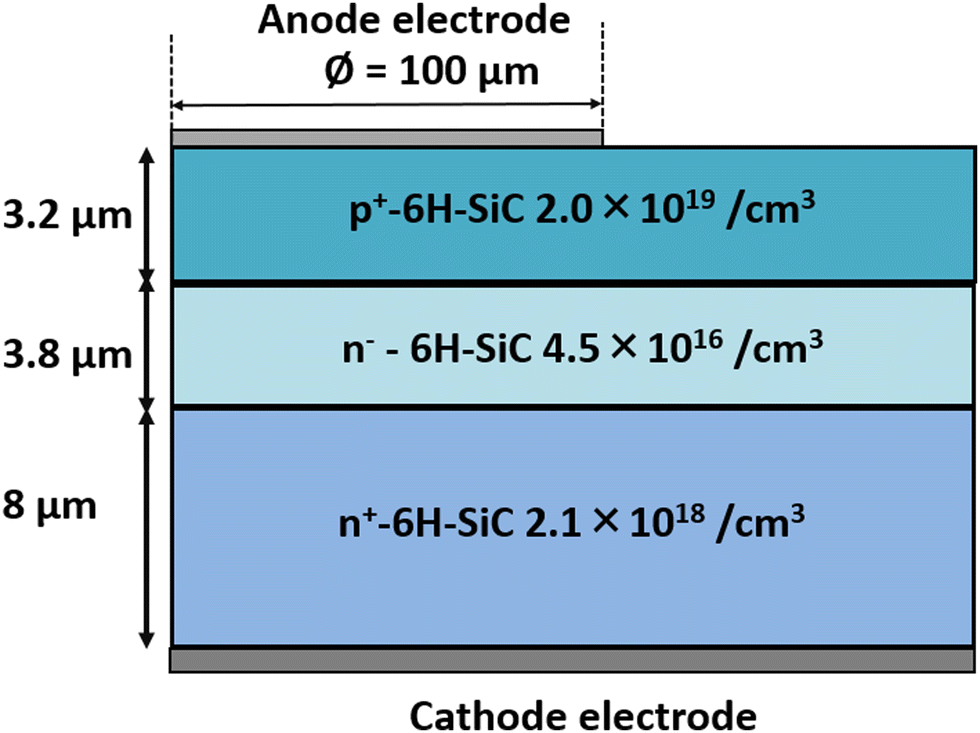
Fig. 1 depicts a schematic representation of a simulated GaN/β-Ga2O3 heterojunction p–n diode. This study focuses on simulating the diode and evaluating the reliability of its reverse recovery characteristics using technology computer-aided design (TCAD) tools. The n-Ga2O3 epitaxial layer has a thickness of 3.8 μm and a doping concentration of 4.5 × 1016 cm−3, while the n-Ga2O3 substrate has a thickness of 8.0 μm and a doping concentration of 2.1 × 1018 cm−3.29,31 The p-GaN layer has a thickness of 3.2 μm and a doping concentration of 2.0 × 1019 cm−3. The material properties of β-Ga2O3 and GaN, such as bandgap, electron mobility, electron affinity, dielectric constant, and thermal conductivity, were obtained from previous research2,21,22,32–34,35–40 and are summarized in Tables 1 and 2, respectively. To calibrate the simulation model, experimental results from β-Ga2O3 Schottky barrier diode (SBD)25 and GaN p–n diode41 were utilized. The simulated I–V characteristics closely match the reported experimental data, as shown in Fig. 2(a) for the Ga2O3 SBD and Fig. 2(b) for the GaN p–n diode.
 |
| | Fig. 1 Schematic representation of the simulated GaN/β-Ga2O3 heterojunction p–n diode. | |
Table 1 Fundamental material properties of β-Ga2O3 used in the simulation
| Parameter |
Value |
| Bandgap (eV) |
4.8 (ref. 21) |
| Conduction band offset (eV) |
0.165 (ref. 32) |
| Valence band offset (eV) |
1.625 (ref. 32) |
| Electron mobility (cm2 V−1 s−1) |
118 (ref. 22) |
| Hole mobility (cm2 V−1 s−1) |
10 (ref. 22) |
| Thermal conductivity (W cm−1 K−1) |
0.13 (ref. 2) |
| Dielectric constant |
10.2 (ref. 33) |
| Electron affinity (eV) |
4.0 (ref. 21) |
| Effective density of states in the conduction band/valence band (cm−3) |
3.72 × 10¹⁸ (ref. 21) |
| Effective density of states in the valence band (cm−3) |
1.16 × 10¹⁹ (ref. 21) |
| Impact inonization coefficients an (cm−1) |
0.79 × 10⁶ (ref. 34) |
| Impact inonization coefficients bn (V cm−1) |
2.92 × 10⁶ (ref. 34) |
| Electron lifetime (s) |
2.0 × 10⁻¹⁰ (ref. 22) |
| Hole lifetime (s) |
2.1 × 10⁻⁸ (ref. 22) |
Table 2 Fundamental material properties of GaN used in the simulation
| Parameter |
Value |
| Bandgap (eV) |
3.53 (ref. 35) |
| Dielectric constant |
8.9 (ref. 36) |
| Electron affinity (eV) |
4.1 (ref. 37) |
| Effective density of states in the conduction band (cm−3) |
2.3 × 10¹⁸ (ref. 38) |
| Effective density of states in the valence band (cm−3) |
3.5 × 10¹⁹ (ref. 38) |
| Impact inonization coefficients an (cm−1) |
1.56 × 10⁵ (ref. 39) |
| Impact inonization coefficients bn (V cm−1) |
1.41 × 10⁷ (ref. 39) |
| Electron lifetime (s) |
1.0 × 10⁻⁹ (ref. 40) |
| Hole lifetime (s) |
1.0 × 10⁻⁹ (ref. 40) |
 |
| | Fig. 2 Experimental data (blue) and simulated data (red) for the forward current–voltage (I–V) characteristics of (a) β-Ga2O3 SBD and (b) GaN p–n diode. Good agreement confirms the accuracy of the DC device model. | |
2.2. Models and parameters used in simulations
The performance of the device was evaluated using 2D device simulators that solve Poisson's equation, along with the continuity and drift-diffusion equations.42–48 These simulations, which also included mixed-mode analyses, were conducted using TCAD tools. During the forward turn-on phase, the p–n junction is positively biased, allowing for carrier conduction. When the device transitions to the off state, the transverse electric field drives the non-equilibrium carriers within the device back to equilibrium. The simulation of the GaN/β-Ga2O3 heterojunction p–n diode incorporates key physical models such as Shockley–Read–Hall and Auger recombination to account for carrier recombination mechanisms, concentration-dependent mobility, and lateral electric field-dependent mobility to capture variations in carrier transport behavior. Additionally, bandgap narrowing is included to model changes in the energy band structure under specific conditions.
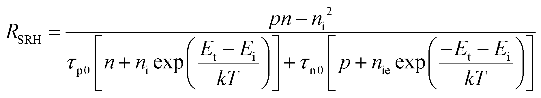
(1) Carrier generation–recombination models: the numerical simulation of carrier generation and recombination is carried out using concentration-dependent models for Shockley–Read–Hall (SRH) and Auger recombination.46–48
| |  | (1) |
| | | RAuger = 3 × 10⁻²⁹(pn2 − nni2) + 3 × 10⁻²⁹(np2 − pni2) | (2) |
Here, ni represents the effective intrinsic carrier concentration, Et denotes the recombination center energy level, Ei is the intrinsic Fermi level, and τn0 and τp0 represent the electron and hole lifetimes, respectively.
(2) Impact inonization model: the equation describes the rate of carrier generation during the avalanche breakdown process.49
Here, αn and αp represent the impact ionization coefficients for electrons and holes, respectively, while Jn and Jp denote the electron and hole current densities. The ionization rate is effectively modeled using the Selberherr model.
| |  | (4) |
Here,
E represents the electric field along the direction of current flow, and
An,p,
Bn,p, and
Cn,p are the respective fitting coefficients.
(3) Thermal conductivity specification: we performed 2D physics-based electrothermal device simulations through TCAD.50 These simulations involved solving coupled drift-diffusion and heat flow equations.
3. Results and discussion
We used TCAD to simulate the band diagram of the heterojunction, as shown in Fig. 3. By selecting the appropriate electron affinity values for GaN and Ga2O3, we obtained a conduction band offset (ΔEc) of 0.165 eV and a valence band offset (ΔEv) of 1.625 eV. These values were chosen to match the required band offsets, in accordance with experimental data. The resulting band offset values are consistent with those reported by W. Li et al.32 using X-ray photoelectron spectroscopy.
 |
| | Fig. 3 Simulated band diagram of the p-GaN/n-β-Ga2O3 heterojunction. | |
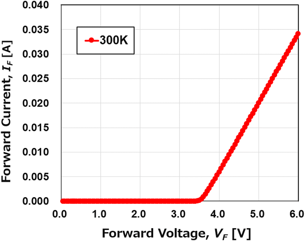
The simulated forward current–voltage (I–V) characteristics of the GaN/β-Ga2O3 p–n diode at 300 K are illustrated in Fig. 4. When a forward bias is applied, the diode exhibits rectifying behavior, and the turn-on voltage is the point at which the current begins to increase. The turn-on voltage (Von) is observed to be 3.5 V, which is in reasonable agreement with experimental results.28
 |
| | Fig. 4 Simulated forward current–voltage (I–V) characteristics of the GaN/β-Ga2O3 p–n diode at 300 K. | |
Fig. 5 illustrates the simulated temperature-dependent forward current–voltage characteristics of the GaN/β-Ga2O3 p–n diode. It can be observed that the turn-on voltage (Von) decreases from 3.5 V to 3.25 V, and the specific on-resistance (Ron,sp) in the current range from 0.02 A to 0.03 A decreases from 5.9 mΩ cm2 to 5.5 mΩ cm2 as the temperature rises from 300 K to 450 K. The decrease in turn-on voltage can be attributed to the increase in diffusion current across the p–n heterojunction and the bandgap narrowing effect at higher temperatures. Similarly, the decrease in Ron,sp with increasing temperature can be explained by the thermally enhanced conductivity modulation effect. As the temperature rises, the injection of minority carriers (holes) from p-GaN into n-β-Ga2O3 increases, leading to a decrease in space-charge resistance in the drift region. Additionally, the thermal generation of electron–hole pairs increases at higher temperatures, improving the conductivity of the drift region and resulting in more efficient current conduction.
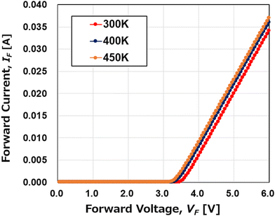 |
| | Fig. 5 Simulated temperature-dependent forward current–voltage (I–V) characteristics of the GaN/β-Ga2O3 p–n diode. | |
Fig. 6 illustrates the simulated temperature-dependent reverse breakdown characteristics of the GaN/β-Ga2O3 heterojunction p–n diode. It is found that the breakdown voltage remains consistent at 703 V across various temperatures, indicating the excellent temperature stability of the diode. The sharp increase in reverse current near the breakdown voltage suggests that the breakdown is dominated by avalanche breakdown. This occurs when high-energy carriers generate additional charge carriers through impact ionization, resulting in an accelerated current flow. Furthermore, Y. Duan et al. reported that the measured breakdown voltage increases with rising temperature, indicating that the diode with a triple-zone junction termination extension structure achieves avalanche-limited breakdown.51 These findings demonstrate the excellent temperature stability of the p-GaN/n-β-Ga2O3 diode and confirm its ability to achieve avalanche-limited breakdown. In addition, Fig. 7 displays the electric field distribution at breakdown for the GaN/β-Ga2O3 p–n diode. The analysis clearly reveals a significant concentration of the electric field at the p-GaN and n-Ga2O3 junction, which can lead to catastrophic damage at this location. These results suggest that using β-Ga2O3 material in heterojunction p–n diodes has the potential to achieve high breakdown voltages by minimizing electric field concentration and leakage current. This highlights the potential application of the p-GaN/n-Ga2O3 heterojunction diode as a power device for high-voltage operations.
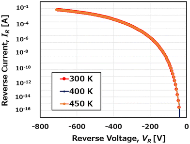 |
| | Fig. 6 Simulated temperature-dependent reverse breakdown characteristics of the GaN/β-Ga2O3 p–n diode. | |
 |
| | Fig. 7 Simulated electric field distributions of the GaN/β-Ga2O3 p–n diode at breakdown: (a) two-dimensional distribution of the electric field; (b) line profile of the electric field along A1–A2. | |
The reverse recovery characteristics of the GaN/β-Ga2O3 p–n diode were investigated and compared to those of the 6H-SiC p–n diode under the same dI/dt conditions. Fig. 8 illustrates the cross-sectional schematic of the 6H-SiC p–n diode used for comparison with the GaN/β-Ga2O3 p–n diode.52 The 6H-SiC p–n diode consists of a 3.8-μm-thick n-type epitaxial layer on an 8-μm-thick n+-type 6H-SiC substrate with a doping concentration of approximately 2.1 × 1018 cm−3. The n-type epitaxial layer has a doping concentration of about 4.5 × 1016 cm−3. The device also includes a 3.2-μm-thick p+-type 6H-SiC layer with a doping concentration of approximately 2.0 × 1019 cm−3. The material parameters for 6H-SiC are provided in Table 3.53 For simulating the reverse recovery characteristics, the parameters for the diode components were set as follows: a reverse voltage (VR) of −10 V and a forward current (IF) of 3 A. The results of this comparison are presented in Fig. 9, along with a summary of the values for the peak reverse recovery current (Irr) and recovery time (trr) for both the GaN/β-Ga2O3 p–n diode and the 6H-SiC p–n diode in Table 4. Here, the peak reverse recovery current (Irr) is defined as the current that occurs during the removal of stored charges in the drift region when the diode switches from the on-state to the off-state. Reverse recovery time (trr) refers to the time it takes for the switching diode to transition from the on-state to the fully off-state.
 |
| | Fig. 8 Schematic representation of the simulated 6H-SiC p–n diode.52 | |
Table 3 Fundamental material properties of 6H-SiC used in the simulation53
| Parameter |
Value |
| Bandgap (eV) |
2.9 |
| Electron lifetime (s) |
1.0 × 10⁻⁹ |
| Hole lifetime (s) |
1.0 × 10⁻⁹ |
| Electron mobility (cm2 V−1 s−1) |
330 |
| Thermal conductivity (W cm−1 K−1) |
5.0 |
| Dielectric constant |
9.66 |
| Electron saturation velocity (cm s−1) |
2.0 × 10⁷ |
| Effective density of states in the conduction band (cm−3) |
7.68 × 10¹⁸ |
| Effective density of states in the valence band (cm−3) |
4.76 × 10¹⁸ |
 |
| | Fig. 9 Simulated reverse recovery characteristics of the GaN/β-Ga2O3 p–n diode compared to the 6H-SiC p–n diode at 300 K. | |
Table 4 Summary of reverse recovery characteristics
| Parameter |
GaN/β-Ga2O3 p–n diode |
6H-SiC p–n diode |
|
I
rr (A) |
7.5 |
19.1 |
|
t
rr (ns) |
72 |
83 |
The results presented in Fig. 9 and Table 4 demonstrate that the GaN/β-Ga2O3 diode has better recovery characteristics than the 6H-SiC diode, with lower Irr and faster recovery time. The reverse recovery time (trr) is calculated from the moment when the current crosses zero until the reverse recovery current decreases to 10% of Irr. The presence of electron traps and gallium vacancies in Ga2O3 plays a crucial role in enhancing minority carrier recombination, thereby reducing both the reverse recovery time (trr) and the reverse recovery current (Irr). In our simulations, defects such as electron and hole traps have been carefully incorporated to reflect their impact on carrier dynamics and diode performance. Previous studies have reported electron traps located near Ec − 0.6 eV, Ec − 0.75 eV, and Ec − 1.05 eV in epitaxial β-Ga2O3 films, as well as the E1, E2, and E3 traps in bulk Ga2O3 crystals.54–59 Additionally, gallium vacancies, which often form in oxygen-rich environments or during annealing processes, act as electron traps and form high-binding-energy gallium–oxygen vacancy complexes that capture returning holes, further improving the reverse recovery characteristics.60 Furthermore, we have compared the simulated reverse recovery characteristics of the p-GaN/n-Ga2O3 diode with the experimental results reported for the Si ultrafast diode STTH3012D,61 as shown in Fig. 10. It is evident that the reverse recovery characteristics of the GaN/β-Ga2O3 diode are superior to those of the Si ultrafast diode STTH3012D. These findings, which are consistent with our defect-inclusive simulations, demonstrate the superior reverse recovery performance of the p-GaN/n-Ga2O3 diode.
 |
| | Fig. 10 Comparison of reverse recovery current for the GaN/β-Ga2O3 p–n diode and the Si ultrafast diode STTH3012D.61 | |
Fig. 11 and 12 depict the temperature and forward current dependence of the reverse recovery characteristics of the GaN/β-Ga2O3 p–n diode. In standard diodes, the reverse recovery time and peak reverse recovery current typically increase with temperature due to the accumulation of holes in the n-layer when a forward bias is applied. During the reverse recovery phase, the depletion region extends from the p–n junction into the n-layer. If the width of the depletion region is smaller than the n-layer, the remaining holes in the n-layer recombine and disappear. As the temperature rises, the carrier lifetime increases, causing a delay in recombination and resulting in a longer reverse recovery time. Additionally, as the accumulated holes recombine and the anode voltage recovers, the reverse recovery current continues to rise, leading to an increase in the peak reverse recovery current. When the forward current is high, both holes and electrons traverse the junction and enter the opposite region. It takes time for these holes to return, thus the reverse recovery time (trr) becomes longer as the forward current increases.
 |
| | Fig. 11 Simulated temperature-dependent reverse recovery characteristics of the GaN/β-Ga2O3 p–n diode. | |
 |
| | Fig. 12 Simulated forward current-dependent reverse recovery characteristics of the GaN/β-Ga2O3 p–n diode. | |
However, Fig. 11 and 12 demonstrate that the reverse recovery waveforms of the GaN/β-Ga2O3 diode are not affected by changes in temperature or the magnitude of the forward current. Both the peak reverse recovery current (Irr) and recovery time (trr) remain nearly constant, regardless of increases in temperature or forward current. This can be attributed to the short carrier lifetimes in both GaN and β-Ga2O3. The electron lifetime and hole lifetime of n-Ga2O3 are 2.0 × 10⁻¹⁰ s and 2.1 × 10⁻⁸ s,22 respectively, while both the electron and hole lifetimes of p-GaN are 1.0 × 10⁻⁹ s.40 Additionally, the excellent property of a large critical electric field in GaN and β-Ga2O3 wide-bandgap materials results in a strong electric field in the depletion region, which quickly sweeps out charge carriers and reduces recovery time. Furthermore, the good thermal conductivity of GaN and optimized device design help to minimize the impact of temperature. In contrast, conventional narrow-bandgap semiconductors typically have longer carrier lifetimes and increased reverse recovery time (trr) at higher temperatures. The independence of the diode's reverse recovery characteristics from the forward current (IF) indicates minimal accumulation of minority carriers, which is due to the optimized layer design of the p-GaN/n-Ga2O3 diode structure in this study. The n-Ga2O3 epitaxial layer has a moderate doping concentration of 4.5 × 1016 cm−3 and a thickness of 3.8 μm, while the n-Ga2O3 substrate has a higher doping concentration of 2.1 × 1018 cm−3 and a thickness of 8.0 μm. This design minimizes stored charge during forward conduction, reducing its impact on reverse recovery. In comparison, other structures with lower doping and thicker epitaxial layers were found to store more charge, resulting in increased Irr and trr at higher forward currents. The optimized structure design in our study ensures stable reverse recovery performance, making it suitable for high-speed switching applications. Additionally, F. Zhou et al.62 also reported that the reverse recovery waveform is dominated by capacitive ringing rather than minority carrier recombination in the NiO/Ga2O3 p–n heterojunction diode.
In addition to the effects of temperature and forward current, the doping concentrations of the n-Ga2O3 epitaxial layer and the p-GaN layer significantly influence the reverse recovery characteristics of the GaN/β-Ga2O3 p–n diode. Therefore, our study has been expanded to investigate how variations in doping concentration affect the reverse recovery time (trr) and peak reverse recovery current (Irr). We believe that by optimizing the doping levels in the n-Ga2O3 and p-GaN layers, the diode's switching performance and breakdown voltage can be improved. Fig. 13 and 14 demonstrate that the reverse recovery characteristics of the GaN/β-Ga2O3 p–n diode are more affected by changes in the doping concentration of the n-Ga2O3 epitaxial layer than those in the p-GaN layer. As the doping concentration of the n-Ga2O3 epitaxial layer increases, both the peak reverse recovery current (Irr) and recovery time (trr) of the GaN/β-Ga2O3 diode also increase. This is because the n-Ga2O3 layer acts as the drift region, storing charge carriers during forward conduction. A higher doping concentration results in a larger amount of stored charge, leading to a higher reverse recovery current and a longer recovery time. This effect is further amplified by the relatively short electron lifetime (2.0 × 10⁻¹⁰ s) and longer hole lifetime (2.1 × 10⁻⁸ s) in the n-Ga2O3 layer. The short electron lifetime allows for rapid electron removal, while the longer hole lifetime delays recombination, thereby extending the reverse recovery time. In contrast, the electron and hole lifetimes of approximately 1.0 ns in the p-GaN layer40 primarily affect the forward conduction process rather than the reverse recovery. Therefore, changes in the doping concentration of the n-Ga2O3 layer have a greater impact on the reverse recovery characteristics of the GaN/β-Ga2O3 p–n diode than those in the p-GaN layer.
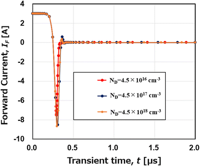 |
| | Fig. 13 Simulated n-Ga2O3 epitaxial layer doping concentration-dependent reverse recovery characteristics of the GaN/β-Ga2O3 p–n diode. | |
 |
| | Fig. 14 Simulated p-GaN layer doping concentration-dependent reverse recovery characteristics of the GaN/β-Ga2O3 p–n diode. | |
4. Conclusion
Our simulations of the GaN/β-Ga2O3 p–n heterojunction diode showed a turn-on voltage of 3.5 V and a breakdown voltage of 703 V at 300 K, with stable performance across different temperatures. This stability highlights the potential application of the p-GaN/n-Ga2O3 heterojunction diode as a reliable power device for high-voltage operations. In the reverse recovery simulation, the GaN/β-Ga2O3 diode demonstrated fast switching behavior, surpassing that of 6H-SiC diodes. Furthermore, the reverse recovery characteristics were found to be unaffected by temperature or the magnitude of the forward current, suggesting that the device primarily operates with majority carriers and is not affected by minority carrier recombination. The optimized structure design presented in our study significantly reduces the impact of temperature and forward current magnitude on the reverse recovery characteristics of the p–n heterojunction diode. Our study also revealed that the reverse recovery characteristics are solely dependent on the doping concentration of the n-Ga2O3 epitaxial layer, rather than the doping concentration of the p-GaN layer. These findings highlight the significant potential of GaN/β-Ga2O3 diodes for applications requiring fast switching, low loss, and high reliability, such as electric vehicles, aerospace, renewable energy systems, and next-generation power devices.
Author contributions
All authors contributed equally to this work. The manuscript was written through contributions of all authors. All authors have given approval to the final version of the manuscript
Declaration of generative AI in scientific writing
There is no generative AI in scientific writing.
Ethics approval
No experiments on animal or human subjects were used for the preparation of the submitted manuscript.
Data availability
The data that support the findings of this study are available from the corresponding author upon reasonable request.
Conflicts of interest
There are no conflicts of interest to declare.
Acknowledgements
The authors would like to express their gratitude to Prof. Cong-Kha Pham of the University of Electro-Communications (UEC), Tokyo, Japan, and the VLSI Design and Education Center (VDEC) at the University of Tokyo, Tokyo, Japan, for their support in providing simulation tools.
References
- S. J. Pearton, J. Yang, P. H. Cary, F. Ren, J. Kim, M. J. Tadjer and M. A. Mastro, A review of Ga2O3 materials, processing, and devices, Appl. Phys. Rev., 2018, 5(1), 011301 Search PubMed.
- C. Wang, J. Zhang, S. Xu, C. Zhang, Q. Feng, Y. Zhang, J. Ning, S. Zhao, H. Zhou and Y. Hao, Progress in state-of-the-art technologies of Ga2O3 devices, J. Phys. D: Appl. Phys., 2021, 54(24), 243001 CrossRef CAS.
- J. Zhang, J. Shi, D.-C. Qi, L. Chen and K. H. L. Zhang, Recent progress on the electronic structure, defect, and doping properties of Ga2O3, APL Mater., 2020, 8(2), 020906 CrossRef CAS.
-
M. Liao, B. Shen and Z. Wang, Progress in semiconductor β-Ga2O3, Ultra-Wide Bandgap Semiconductor Materials (Materials Today), Elsevier, Amsterdam, The Netherlands, 2019, pp. 263–345 Search PubMed.
- J. Montes, C. Kopas, H. Chen, X. Huang, T.-H. Yang, K. Fu, C. Yang, J. Zhou, X. Qi, H. Fu and Y. Zhao, Deep level transient spectroscopy investigation of ultra-wide bandgap (−201) and (001) β-Ga2O3, J. Appl. Phys., 2020, 128(20), 205701 CrossRef CAS.
- M. Bosi, P. Mazzolini, L. Seravalli and R. Fornari, Ga2O3 polymorphs: tailoring the epitaxial growth conditions, J. Mater. Chem. C, 2020, 8(32), 10975–10992 RSC.
- D. Guo, Q. Guo, Z. Chen, Z. Wu, P. Li and W. Tang, Review of Ga2O3-based optoelectronic devices, Mater. Today Phys., 2019, 11, 100157 CrossRef.
- H. Aida, K. Nishiguchi, H. Takeda, N. Aota, K. Sunakawa and Y. Yaguchi, Growth of β-Ga2O3 Single Crystals by the Edge-Defined, Film Fed Growth Method, Jpn. J. Appl. Phys., Part 1, 2008, 47, 8506 CrossRef CAS.
- R. Singh, T. R. Lenka, D. K. Panda, R. T. Velpula, B. Jain, H. Q. T. Bui and H. P. T. Nguyen, The dawn of Ga2O3 HEMTs for high power electronics – A review, Mater. Sci. Semicond. Process., 2020, 119, 105216 CrossRef CAS.
- H. Zhou, J. Zhang, C. Zhang, Q. Feng, S. Zhao, P. Ma and Y. Hao, A review of the most recent progresses of state-of-art gallium oxide power devices, J. Semicond., 2019, 40(1), 011803 CrossRef CAS.
- M. Higashiwaki, K. Sasaki, A. Kuramata, T. Masui and S. Yamakoshi, Development of gallium oxide power devices, Phys. Status Solidi A, 2014, 211(1), 21–26 CrossRef CAS.
- M. H. Wong and M. Higashiwaki, Vertical β-Ga2O3 power transistors: a review, IEEE Trans. Electron Devices, 2020, 67(10), 3925–3937 CAS.
- K. Konishi, K. Goto, H. Murakami, Y. Kumagai, A. Kuramata, S. Yamakoshi and M. Higashiwaki, 1-kV vertical Ga2O3 field-plated Schottky barrier diodes, Appl. Phys. Lett., 2017, 110(10), 103506 CrossRef.
- H. Fu, H. Chen, X. Huang, I. Baranowski, J. Montes, T. H. Yang and Y. Zhao, A comparative study on the electrical properties of vertical (−201) and (010) β-Ga2O3 Schottky barrier diodes on EFG single-crystal substrates, IEEE Trans. Electron Devices, 2018, 65(8), 3507–3513 CAS.
- M. Higashiwaki, K. Sasaki, T. Kamimura, M. H. Wong, D. Krishnamurthy, A. Kuramata, T. Masui and S. Yamakoshi, Depletion-mode Ga2O3 metal-oxide-semiconductor field-effect transistors on β-Ga2O3 (010) substrates and temperature dependence of their device characteristics, Appl. Phys. Lett., 2013, 103, 123511 CrossRef.
- M. H. Wong, K. Sasaki, A. Kuramata, S. Yamakoshi and M. Higashiwaki, Field-Plated Ga2O3 MOSFETs With a Breakdown Voltage of Over 750 V, IEEE Electron Device Lett., 2016, 37(2), 212–215 CAS.
- A. J. Green, K. D. Chabak, E. R. Heller, R. C. Fitch, M. Baldini, A. Fiedler, K. Irmscher, G. Wagner, Z. Galazka, S. E. Teltak, A. Crespo, K. Leedy and G. H. Jessen, 3.8-MV cm−1 Breakdown Strength of MOVPE-Grown Sn-Doped β-Ga2O3 MOSFETs, IEEE Electron Device Lett., 2016, 37(7), 902–905 Search PubMed.
- S. Krishnamoorthy, Z. Xia, S. Bajaj, M. Brenner and S. Rajan, Delta-doped β-gallium oxide field-effect transistor, Appl. Phys. Express, 2017, 10, 051102 CrossRef.
- E. Ahmadi, O. S. Koksaldi, X. Zheng, T. Mates, Y. Oshima, U. K. Mishra and J. S. Speck, Demonstration of β-(AlxGa1−x)2O3/β-Ga2O3 modulation doped field-effect transistors with Ge as dopant grown via plasma-assisted molecular beam epitaxy, Appl. Phys. Express, 2017, 10, 071101 CrossRef.
- N. Moser, J. McCandless, A. Crespo, K. Leedy, A. Green, A. Neal, S. Mou, E. Ahmadi, J. Speck, K. Chabak, N. Peixoto and G. Jessen, Ge-Doped β-Ga2O3 MOSFETs, IEEE Electron Device Lett., 2017, 38(6), 775–778 CAS.
- M. Higashiwaki, K. Sasaki, A. Kuramata, T. Masui and S. Yamakoshi, Gallium oxide (Ga2O3) metal–semiconductor field-effect transistors on single-crystal β-Ga2O3 (010) substrates, Appl. Phys. Lett., 2012, 100, 013504 CrossRef.
- K. Wang, Z. Wang, R. Cao, H. Liu, W. Chang, L. Zhao, B. Mei, H. Lv, X. Zeng and Y. Xue, Study of the mechanism of single event burnout in lateral depletion-mode Ga2O3 MOSFET devices via TCAD simulation, J. Appl. Phys., 2024, 135, 145702 CrossRef CAS.
- H. H. Gong, X. H. Chen, Y. Xu, F.-F. Ren, S. L. Gu and J. D. Ye, A 1.86-kV double-layered NiO/β-Ga2O3 vertical p–n heterojunction diode, Appl. Phys. Lett., 2020, 117, 022104 CrossRef CAS.
- W. Hao, Q. He, K. Zhou, G. Xu, W. Xiong, X. Zhou, G. Jian, C. Chen, X. Zhao and S. Long, Low defect density and small I–V curve hysteresis in NiO/β-Ga2O3 pn diode with a high PFOM of 0.65 GW cm−2, Appl. Phys. Lett., 2021, 118, 043501 CrossRef CAS.
- T. Watahiki, Y. Yuda, A. Furukawa, M. Yamamura, Y. Takiguchi and A. Miyajima, Heterojunction p-Cu2O/n-Ga2O3 diode with high breakdown voltage, Appl. Phys. Lett., 2017, 111, 222104 CrossRef.
- H. Gong, F. Zhou, W. Xu, X. Yu, Y. Xu, Y. Yang, F. Ren, S. Gu, Y. Zheng, R. Zhang, H. Lu and J. Ye, 1.37 kV/12 A NiO/β-Ga2O3 Heterojunction Diode With Nanosecond Reverse Recovery and Rugged Surge-Current Capability, IEEE Trans. Power Electron., 2021, 36(11), 12213–12217 Search PubMed.
- X. Lu, X. Zhou, H. Jiang, Z. Chen, Y. Pei, K. M. Lau and G. Wang, 1-kV Sputtered p-NiO/n-Ga2O3 Heterojunction Diodes with an Ultra-Low Leakage Current Below 1 μA cm−2, IEEE Electron Device Lett., 2020, 41(3), 449–452 CAS.
- J. Montes, C. Yang, H. Fu, T.-H. Yang, K. Fu, H. Chen, J. Zhou, X. Huang and Y. Zhao, Demonstration of mechanically exfoliated β-Ga2O3/GaN p–n heterojunction, Appl. Phys. Lett., 2019, 114(16), 162103 CrossRef.
- D. H. Mudiyaselage, D. Wang and H. Fu, Wide Bandgap Vertical kV-class β-Ga2O3/GaN Heterojunction p–n Power Diodes with Mesa Edge Termination, IEEE J. Electron Devices Soc., 2022, 10, 89–97 Search PubMed.
- E. Hossain, A. A. Rahman, M. Gokhale, R. Kulkarni, R. Mondal, A. Thamizhavel and A. Bhattacharya, Growth of high-quality GaN on (1 0 0) Ga2O3 substrates by facet-controlled MOVPE, J. Cryst. Growth, 2019, 524, 125165 CrossRef CAS.
- S. Leone, R. Fornari, M. Bosi, V. Montedoro, L. Kirste, P. Doering, F. Benkhelifa, M. Prescher, C. Manz, V. Polyakov and O. Ambacher, Epitaxial growth of GaN/Ga2O3 and Ga2O3/GaN heterostructures for novel high electron mobility transistors, J. Cryst. Growth, 2020, 534, 125511 CrossRef CAS.
- W. Li, X. Zhang, J. Zhao, J. Yan, Z. Liu, J. Wang, J. Li and T. Wei1, Rectification behavior of polarization effect induced type-II n-GaN/n-type β-Ga2O3 isotype heterojunction grown by metal organic vapor phase epitaxy, J. Appl. Phys., 2020, 127(1), 015302 CrossRef CAS.
- K. Irmscher, Z. Galazka, M. Pietsch, R. Uecker and R. Fornari, Electrical properties of β-Ga2O3 single crystals grown by the Czochralski method, J. Appl. Phys., 2011, 110(6), 063720 CrossRef.
- K. Ghosh and U. Singisetti, Impact ionization in β-Ga2O3, J. Appl. Phys., 2018, 124(8), 085707 CrossRef.
- I. Vurgaftman, J. R. Meyer and L. R. Ram-Mohan, Band parameters for III–V compound semiconductors and their alloys, J. Appl. Phys., 2001, 89(11), 5815–5875 CrossRef CAS.
-
O. Madelung, U. Rössler and M. Schulz, Group IV Elements, IV–IV and III–V Compounds. Part b – Electronic, Transport, Optical and Other Properties, Springer-Verlag, Berlin Heidelberg, 2002 Search PubMed.
- S. N. Mohammad and H. Morkoç, Progress and prospects of group-III nitride semiconductors, Prog. Quantum Electron., 1996, 20(5–6), 361–525 CrossRef CAS.
- G. Sabui, P. J. Parbrook, M. Arredondo-Arechavala and Z. J. Shen, Modeling and simulation of bulk gallium nitride power semiconductor devices, AIP Adv., 2016, 6(5), 055006 CrossRef.
- B. J. Baliga, Gallium nitride devices for power electronic applications, Semicond. Sci. Technol., 2013, 28, 074011 CrossRef.
- G. F. Brown, J. W. Ager, W. Walukiewicz and J. Wu, Finite element simulations of compositionally graded InGaN solar cells, Sol. Energy Mater. Sol. Cells, 2010, 94, 478–483 CrossRef CAS.
- X. A. Cao, H. Lu, S. F. LeBoeuf, C. Cowen, S. D. Arthur and W. Wang, Growth and characterization of GaN PiN rectifiers on free-standing GaN, Appl. Phys. Lett., 2005, 114(87), 053503 CrossRef.
- C. Liu, E. F. Chor and L. S. Tan, Enhanced device performance of AlGaN/GaN HEMTs using HfO2 high-k dielectric for surface passivation and gate oxide, Semicond. Sci. Technol., 2007, 22, 522–527 CrossRef CAS.
- M. Ruff, H. Mitlenher and R. Helbig, SiC devices: physics and numerical simulation, IEEE Trans. Electron Devices, 1994, 41, 1040–1054 CrossRef CAS.
- P. T. Landsberg and G. S. Kousik, The connection between carrier lifetime and
doping density in nondegenerate semiconductors, J. Appl. Phys., 1984, 56, 1696–1700 CrossRef CAS.
- A. Galeckas, J. Linnros, V. Grivickas, U. Lindefelf and C. Hallin, Auger recombination in 4H-SiC: unusual temperature behaviour, Appl. Phys. Lett., 1997, 71, 3269–3271 CrossRef CAS.
-
P. Losee, Design, fabrication and characterization of high voltage 4H-SiC junction rectifiers for power switching application, PhD dissertation, Rensselaer Polytechnic Institute, New York, 2007 Search PubMed.
- Q. Song, T. Xiaoyan, H. Yuan, C. Han and Y. Zhang, Design, Simulation and Fabrication of 4H-SiC power SBDs with SIPOS FP structure, IEEE Trans. Device Mater. Reliab., 2015, 15, 543–551 CAS.
-
S. M. Sze, Physics of Semiconductor devices, Wiley, New York, NY, USA, 1981 Search PubMed.
- R. Raghunathan and B. J. Baliga, Temperature dependence of hole impact ionization coefficients in 4H and 6H-SiC, Solid-State Electron., 1999, 43(2), 199–211 CrossRef CAS.
- M. H. Wong, Y. Morikawa, K. Sasaki, A. Kuramata, S. Yamakoshi and M. Higashiwaki, Characterization of channel temperature in Ga2O3 metal-oxide-semiconductor field-effect transistors by electrical measurements and thermal modeling, Appl. Phys. Lett., 2016, 109, 193503 CrossRef.
- Y. Duan, J. Wang, Z. Zhu, G. Piao, K. Ikenaga, H. Tokunaga, S. Koseki, M. Bulsara and P. Fay, Ion-implanted triple-zone graded junction termination extension for vertical GaN p–n diodes, Appl. Phys. Lett., 2023, 122, 212104 CrossRef CAS.
- K. Fujihira, S. Tamura, T. Kimoto and H. Matsunami, Low-Loss, High-Voltage 6H-SiC Epitaxial p–i–n Diode, IEEE Trans. Electron Devices, 2002, 49(1), 150–154 CrossRef CAS.
-
L. Latu-Romain and M. Ollivier, Silicon Carbide One-dimensional Nanostructures, edn 2015, WILEY-ISTE London, United Kingdom, 2015, pp. 1–148 Search PubMed.
- A. Y. Polyakov, N. B. Smirnov, I. V. Shchemerov, E. B. Yakimov, J. Yang, F. Ren, G. Yang, J. Kim, A. Kuramata and S. J. Pearton, Point defect induced degradation of electrical properties of Ga2O3 by 10 MeV proton damage, Appl. Phys. Lett., 2018, 112, 032107 CrossRef.
- Z. Zhang, E. Farzana, A. R. Arehart and S. A. Ringel, Deep level defects throughout the bandgap of (010) β-Ga2O3 detected by optically and thermally stimulated defect spectroscopy, Appl. Phys. Lett., 2016, 108, 052105 CrossRef.
- Y. Nakano, Electrical Characterization of β-Ga2O3 Single Crystal Substrates, ECS J. Solid State Sci. Technol., 2017, 6, 615 CrossRef.
- M. E. Ingebrigtsen, J. B. Varley, A. Y. Kuznetsov, B. G. Svensson, G. Alfieri, A. Mihaila, U. Badstübner and L. Vines, Iron and intrinsic deep level states in Ga2O3, Appl. Phys. Lett., 2018, 112, 042104 CrossRef.
- M. Labed, N. Sengouga, C. V. Prasad, M. Henini and Y. S. Rim, On the nature of majority and minority traps in β-Ga2O3: a review, Mater. Today Phys., 2023, 36, 101155 CrossRef CAS.
- E. Farzana, E. Ahmadi, J. S. Speck, A. R. Arehart and S. A. Ringel, Deep level defects in Ge-doped (010) β-Ga2O3 layers grown by plasma-assisted molecular beam epitaxy, J. Appl. Phys., 2018, 123, 161410 CrossRef.
- K. Zeng, Z. Bian, N. Sinha and S. Chowdhury, Simultaneous drive-in of Mg and disassociation of Mg–H complex in Ga2O3 by oxygen annealing achieving remarkable current blocking, Appl. Phys. Lett., 2024, 124, 212102 CrossRef CAS.
- S. Yin, Y. Liu, Y. Liu, K. J. Tseng, J. Pou and R. Simanjorang, Comparison of SiC Voltage Source Inverters Using Synchronous Rectification and Freewheeling Diode, IEEE Trans. Ind. Electron., 2018, 65(2), 1051–1061 Search PubMed.
- F. Zhou, H. Gong, M. Xiao, Y. Ma, Z. Wang, X. Yu, L. Li, L. Fu, H. H. Tan, Y. Yang, F.-F. Ren, S. Gu, Y. Zheng, H. Lu, R. Zhang, Y. Zhang and J. Ye, An avalanche-and-surge robust ultrawidebandgap heterojunction for power electronics, Nat. Commun., 2023, 14, 4459 CrossRef CAS PubMed.
|
| This journal is © The Royal Society of Chemistry 2025 |
Click here to see how this site uses Cookies. View our privacy policy here. 
 Open Access Article
 This Open Access Article is licensed under a Creative Commons Attribution-Non Commercial 3.0 Unported Licence
 *a,
Tho Quang
Than
b and
Yasushi
Takaki
c
*a,
Tho Quang
Than
b and
Yasushi
Takaki
c