
 Open Access Article
 This Open Access Article is licensed under a Creative Commons Attribution-Non Commercial 3.0 Unported Licence
Eco-friendly CoFe2O4 ferrite nanoparticles prepared using greek yogurt solution: deep insights into optical properties and abnormal semiconductor–insulator–semiconductor transitions for optoelectronics and catalytic applications†
Heba
Hussein
 *,
S. S.
Ibrahim
and
Sherif A.
Khairy
*,
S. S.
Ibrahim
and
Sherif A.
Khairy
Physics Department, Faculty of Science, Cairo University, Cairo 11566, Egypt. E-mail: Heba@sci.cu.edu.eg
First published on 7th March 2025
Abstract
This study introduces a green and cost-effective synthesis method for CoFe2O4 nanoparticles using Greek yogurt, showcasing significant advancements in surface and interface science. The nanoparticles, characterized by a spinel structure with direct and indirect band gaps of 1.46 eV and 0.9 eV, respectively, demonstrate exceptional structural, optical, dielectric, and catalytic properties. Dielectric analysis reveals strong frequency- and temperature-dependent behaviour, with high dielectric constants at low frequencies and conduction mechanisms dominated by polaron hopping and defect states. Using the Havriliak–Negami model, the study highlights temperature-dependent relaxation times and dielectric constants, further elucidating the nanoscale interfacial dynamics governing these phenomena. The nanoparticles achieved a remarkable 97% degradation of H2O2 in just 150 minutes at room temperature, following first-order kinetics with a rate constant of 3.39 × 10⁻⁴ s−1. The superior performance is attributed to their high surface area (269.67 m2 g−1) and small crystallite size (14.78 nm), which optimize their surface and interface properties. By integrating green synthesis methods with advanced insights into interfacial processes, this work bridges the critical link between nanoscale structural features and functional outcomes, establishing CoFe2O4 nanoparticles as ideal candidates for environmentally sustainable optoelectronic and catalytic technologies. This research redefines the intersection of green chemistry and material science, emphasizing the transformative potential of tailoring nanoscale interfaces to drive next-generation sustainable technologies. The findings expand the fundamental understanding of material interfaces and highlight practical pathways for optimizing stability and efficiency in real-world applications, paving the way for breakthroughs in optoelectronics and catalysis.
1. Introduction
Nanomaterials are highly valued across various scientific and technological domains, such as drug delivery, electronics, optics, catalysis, and antibacterial applications. Among these, magnetic nanoparticles (MNPs) stand out due to their magnetic, electrical, physical, and chemical properties, showcasing immense potential in multiple fields. MNPs find utility in information processing, magnetic resonance imaging, magnetic fluids, catalysis, and surface modification. Their ability to undergo surface functionalization makes them particularly promising for drug delivery purposes.1,2 Nanoparticles are synthesized through various methods, such as hydrothermal processing, sol–gel techniques, citrate precursor methods, co-precipitation, and green microemulsion synthesis. Among these, green synthesis stands out as it offers several advantages over physical and chemical approaches, including scalability, cost-effectiveness, and ease of production at a large scale. Unlike traditional methods, green synthesis does not require expensive equipment, hazardous chemicals, high temperatures, or pressure. By utilizing plant extracts (such as seeds, leaves, peels, and flowers), fungi, enzymes, and bacteria, rather than relying heavily on chemicals, this synthesis approach is environmentally friendly.3The distinctive attributes of cobalt ferrite nanoparticles, such as their high magnetocrystalline anisotropy, substantial coercivity, reduced saturation magnetization, elevated hardness, and robustness against thermal and chemical influences, render them suitable candidates for efficiently transporting medications to targeted sites. CoFe2O4 (CFO) nanoparticles belong to the spinel ferrite group, denoted as AB2O4, where A and B represent divalent and trivalent metal ions, respectively.4
Hydrogen peroxide plays a significant role as a reagent in the Fenton reaction, which is employed for the purification of industrial wastewater by removing organic pollutants like dyes and bisphenol A.5–7 In Fenton processes, hydroxyl radicals (HO˙) are generated through the decomposition of H2O2 catalyzed by ferrous ions. The formation of hydroxyl radicals follows the electron transfer mechanism outlined in the Haber–Weiss cycle.8 Small quantities of peroxyl radicals (HO2˙) and molecular oxygen (O2) are also produced. The Fenton process offers advantages such as operating at ambient temperature and requiring simple equipment.9,10 Furthermore, the use of hydrogen peroxide as an oxidant in this process is deemed safe and environmentally friendly.11 Fenton oxidation is effective for elevated levels of organic pollutants, mainly when biological remediation is less practical or advantageous. The primary drawback of Fenton oxidation lies in the requirement to eliminate the ferric ions produced during the catalytic reaction. The concentration of generated ferric ions exceeds the approved threshold value for treated wastewater. Utilizing transition metal oxides as heterogeneous catalysts offers more advantages than traditional Fenton catalysts. Moreover, numerous ferrites possess magnetizable properties, enabling their removal through magnetic traps.12,13
Ferrites’ fundamental understanding and practical applications heavily rely on their dielectric properties. These materials exhibit dielectric behaviour due to their polycrystalline structure, associated with hopping polarization and interfacial phenomena. Previous research has focused on studying the dielectric properties of metal-doped cobalt ferrite CFO and the frequency-dependent permittivity of CFO. Scholars have explored how temperature affects dielectric properties, shedding light on para-ferroelectric phase transitions and overall ferroelectric qualities.14 Numerous studies have investigated ceramic CFO's electrical characteristics and dielectric relaxation in the past decade. However, the underlying processes governing these characteristics and relaxation remain unclear. Dhabekar et al. suggested that Koop's concept, which involves conducting grain interiors and non-conducting grain boundaries, primarily drives the polarization process in CFO ceramics. Conversely, the Maxwell–Wagner model aligns with the relaxation mechanism of alternating current (AC) conductivity.15 According to George et al., the Maxwell–Wagner-type interfacial polarization mechanism mainly accounts for the changes in permittivity and AC conductivity with frequency. Moreover, the increased permittivity and conductivity observed in small grains can be explained by the barrier-hopping concept.16 Routray et al.17 investigated how silver (Ag) doping affects the dielectric and electrical properties of CoFe2O4 (CFO) nanoparticles synthesized using okra extract. Their findings indicate that the dielectric response aligns with the modified Debye model, while the negative dielectric loss suggests a shift in polarization due to changes in the Co2+/Fe2+ ratio. Impedance and modulus studies further revealed that charge carriers, influenced by temperature and frequency, accumulate at grain boundaries. The study also supports the Maxwell–Wagner interfacial polarization mechanism as a key factor behind the observed high dielectric constant. With enhanced dielectric properties, Ag-doped CFO emerges as a potential material for high-frequency applications, sparking ongoing discussions on its polarization behavior across different frequencies.
Similarly, Shanmugavani et al.18 studied the impact of fuel and pH levels on the synthesis of CFO nanoparticles. They found that the dielectric behaviour followed the Maxwell–Wagner interfacial polarization mechanism. Panda et al., in their investigation of the electric transport behaviour of bulk CFO, attributed the high dielectric behaviour to the Maxwell–Wagner polarization mechanism.19 Sharma et al. noted that low-frequency dielectric characteristics are primarily associated with the Maxwell–Wagner polarization mechanism.20 Researchers commonly observe a high dielectric constant in CFO ceramics. The widely accepted internal barrier layer capacitor model, based on the Maxwell–Wagner polarization process, suggests that this high dielectric constant phenomenon stems from the electrically heterogeneous nature of the material.18–20 Current debates focus on the polarization process at low frequencies.
While our previous work21 explored the heavy metal, dye removal efficiency, magnetic, and optical properties of green-synthesized CFO nanoparticles, the present study delves deeper into the role of nanoscale interfaces in governing material behaviour. Specifically, the Maxwell–Wagner type interfacial polarization and its influence on abnormal semiconductor–insulator–semiconductor transitions were investigated. These phenomena, driven by interfacial charge carrier dynamics and defect states, extend the understanding of dielectric properties and open new avenues for tailoring nanoscale interfaces in multifunctional materials.
Building on this foundation, the study pioneers a green and sustainable approach to synthesizing CFO ferrite nanoparticles using Greek yogurt as a natural reducing agent, thereby eliminating the need for toxic chemicals and high-energy processes. It delves into these nanoparticles’ structural, optical, and electrical properties, emphasising their dielectric behaviour and conductivity spectra. By extracting Havriliak–Negami parameters, we uncover intricate relaxation mechanisms and intriguing transitions from semiconducting to insulating states. Moreover, the work advances the understanding of surface and interface phenomena by highlighting the critical role of interfacial polarization at grain and grain boundary interfaces. These interactions, governed by Maxwell–Wagner polarization mechanisms, elucidate the abnormal dielectric transitions observed under varying thermal and electrical stimuli. The study further emphasizes the interplay between the high specific surface area and mesoporosity of CFO nanoparticles, which enhance their catalytic activity by providing abundant active sites and ensuring efficient diffusion pathways for reactants and products. Beyond fundamental insights, this research explores the immense potential of CFO nanoparticles in cutting-edge applications such as optoelectronics, catalysis, and energy storage. The novel focus on surface/interface interactions and their functional implications bridges green synthesis with surface and interface engineering, offering exciting prospects for next-generation efficient and environmentally friendly technologies.
2. Experimental work
2.1. Materials and synthesis of CoFe2O4
The CFO nanoparticles were synthesized using a self-combustion or self-ignition method, as described in our previous work.21 Cobalt and iron nitrates were briefly used as precursors, and a Greek yogurt solution was employed. Detailed synthesis conditions are provided in ref. 21.2.2. Analysis and characterization
The ESI† document provides full details of the instrument specifications and photocatalytic degradation of hydrogen peroxide.3. Results and discussion
3.1. X-ray diffraction (XRD) and Rietveld refinements
X-ray diffraction (XRD) is a valuable method for evaluating the purity of synthesized material. Fig. 1 depicts the refined XRD pattern of the produced CFO nanoparticles. The lattice parameters were determined using a global profile-matching technique with FullProf software. This analysis reveals that the prepared CFO ferrite sample crystallizes in a face-centred cubic structure with an Fd![[3 with combining macron]](https://www.rsc.org/images/entities/char_0033_0304.gif) m space group.
m space group.
 | ||
| Fig. 1 Rietveld refinements of the powder diffraction pattern of the CFO nanoparticles. The inset shows the polyhedron configuration of the face-centred cubic spinel structure of CFO.21 | ||
The R-factors such as (the Bragg factor) RB, (crystallographic factor) RF, (expected profile factor) Rexp, (weighted profile factor) Rw, and the goodness of fit (GOF) were calculated by the equations reported in previous literature.22–24 Table S1 (ESI†) provides the calculated R-factors, goodness of fit (GOF), and χ2 values for the prepared sample, alongside other Rietveld analysis parameters. The low values indicate a strong agreement between the refined model and the experimental observations.
The lattice parameters and unit cell volume are summarized in Table S1 (ESI†). These values are smaller than those reported in the literature.3 The volume of the prepared sample can be expressed as: V = a3. The full details of the refinement were mentioned in our previous work.21 The average crystallite size (D = 14.78 nm) is calculated using the classical Debye–Scherrer equation.25 The average crystallite size is smaller than that obtained by Dhanda. et al.3 The bulk density (ρB) and theoretical X-ray density (X-ray density) (ρx) were computed according to the equation reported in previous literature26 and are listed in Table S1 (ESI†). The obtained discrepancy in density values can be attributed to the porosity21 of the sample (Table S1, ESI†) that formed during the preparation of the sample.
The cation distribution of the eco-friendly cobalt ferrite sample, as estimated in Table S1 (ESI†), was determined using the Bertaut method,27 as described in our earlier work.21
Furthermore, the hopping lengths and polaron radii were calculated using eqn (S1)–(S4) (ESI†) and are presented in Table S2 (ESI†). It is observed that the polaron radius is smaller than the hopping lengths, indicating the formation of small polarons.28 It is also noted that the hopping length of the tetrahedral site (LA) and the tetrahedral octahedral sites (LAB) are longer than that of the octahedral site (LB), which led to the conclusion that the likelihood of charge carrier (electron) hopping between ions at the B and B sites is higher than that between the (A and A) and (A and B) sites, improving the conduction mechanism at the octahedral site.29
Additionally, vacancy model calculations can determine the occupancy of cations and anions in the lattice. The ionic-packing coefficients were calculated using eqn (S5) and (S6) (ESI†) and are listed in Table S2 (ESI†). The Pa is less than 1, indicating the presence of cation or anion vacancies in the tetrahedral sites of the produced sample. According to,30 the low ionic packing coefficient, Pb (less than 1), suggests smaller ion distances and more significant overlap of the cation s and anion p orbitals, implying the presence of cation or anion vacancies. These vacancies act as trapping centres for the charge carriers in our green synthesized cobalt ferrite sample, which will be discussed briefly in the AC conductivity section.
The fulfilment coefficient of the unit cell (αV), which can be calculated using eqn (S7) (ESI†), can be used to determine the degree of ionic packing of the spinel structure. The value of αV is close to 0.64, confirming the previous literature's explanation that our synthesized sample exhibits a mixed spinel structure.31
Moreover, the normalized volume of ions missing at the nodal points of the spinel structure is referred to as the vacancy parameter βV.30 It can be calculated using eqn (S8) (ESI†) and measures the overall number of vacancies present in the material. The estimated vacancy parameter is listed in Table S2 (ESI†). A large value (more than 1) confirms the presence of cation or anion vacancies in the prepared sample.
3.2. Optical properties (DRS measurements)
The CFO sample's UV-Vis-NIR optical absorbance spectrum spanning 190–2400 nm (Fig. 2(a)) exhibits a narrow absorption band at approximately 226 nm. This absorption is attributed to ligand-to-metal charge transfer, specifically from O 2p valence band states to Fe 3d conduction band states. In the visible region (400–800 nm), electronic transitions within the Co d-orbitals, induced by the octahedral crystal field, generate broad absorbance bands.32–34 In this study, the Tanabe Sugano (T–S)35 energy level diagram and crystal field theory were employed to analyze the UV-Vis absorption band in the visible-NIR regions (400–1300 nm). The T–S energy level diagram for Co2+ ions in an octahedral environment (Fig. 3(a)) is accompanied by a spin that enables a potential d–d transition (spin-allowed transitions). Spectroscopic 4F, 4P, 2H, 2G, 2F, and 2D energy terms are produced by the electronic distribution of the free Co2+ ion (d7), where 4F and 4P stand for the ground state and first excited state terms, respectively. In octahedral symmetry, the degeneracy of the 4F term is lifted and separated into three crystal field terms. These terms are derived from the group theory analysis and can be represented as 4F → 4A2g + 4T2g + 4T1g in terms of the Mullikan symbol, where 4T1g is the ground state term. The 4P term is defined by the Mullikan symbol term35 and is unaffected by the octahedral field. Three conspicuous absorption bands in the octahedral environment are produced by the general feature of Co2+ absorption, defined in terms of ligand field theory, as shown in Fig. 3(b). These peaks result from spin-allowed transitions. The energy level splitting of Co2+ (3d7) ions in an octahedral field (Fig. 3(b)) is 4T1g (4F) → 4T2g (4F) (t62ge1g → t52ge2g), 4T1g(4F) → 4A2g(4F) (t52ge2g → t32ge4g), and 4T1g(4F) → 4T1g(4P) (t42ge3g → t32ge4g),33,36 respectively. Fig. 2(b) shows the UV-vis spectrum of the prepared cobalt ferrite sample fitted with a Gaussian multi-peak function. This figure shows that the transitions from the 4T1g ground state to the 4T2g, 4A2g (4F), and 4T1g (4P) excited states are located in the (1164), (780.5), and below (625) nm wavelength ranges, respectively, similar behaviour was reported by R. C. Rai et al.36 Therefore, the broad absorption peak at 230–800 nm is attributed to the 4T1g(4F) → 4A2g(4F) and 4T2g(4F) → 4T1g(4P) electronic transitions. A series of bands with different polarizations are identified, representing the third spin-permitted transition 4T1g(4F) → 4T1g(4P) (orange peaks Fig. 2(b)). The symmetry and distortion of the sites, selection criteria for Co2+ in the sites, and distribution of Co2+ among the nonequivalent structural sites all affect how many components make up each of these bands, which are controlled by the splitting of the electronic states.36 | ||
| Fig. 2 (a) Absorbance spectra of the CFO nanoparticles over the wavelength range of 190–2400 nm. (b) Deconvolution of the broad UV-vis-NIR absorbance peak over the wavelength range of (190–1200). | ||
 | ||
| Fig. 3 (a) Simplified Tanabe–Sugano diagram for octahedral Co2+ (3d7)37 (b) The energy levels of the Co2+ (3d7) ion in an octahedral field with three spin allowed electronic transitions from d to d in CoO6. | ||
The electronic transitions in the CFO sample exhibit mediocre oscillator strengths, as indicated by the spectra (Fig. 3(b)), suggesting slight deformation in the local structure of CoO6, likely due to spin-charge–lattice interactions. This distortion breaks the crystal field symmetry of an octahedral field, enabling d-to-d transitions. Conversely, in FeO6 and FeO4 local structures, Fe3+ ions are in high-spin states, rendering Fe3+ d-to-d transitions parity-forbidden and spin-forbidden. Consequently, Fe3+ d-to-d transitions have negligible oscillator strengths and may not appear in the absorption spectra, as illustrated in Fig. 4. Nonetheless, the prepared CFO sample exhibits broad NIR absorption bands, indicating their potential as candidates for use in near-infrared optoelectronic devices.38
 | ||
| Fig. 4 Crystal field splitting of Fe3+ and Co2+ cation 3d orbitals for tetrahedral and octahedral symmetries. Net spins have been illustrated for every conceivable cation-charge state. | ||
The Kubelka–Munk theory, applied to assess the optical energy gap from the UV-VIS-NIR diffuse reflectance spectra, utilizes the Kubelka–Munk function (F(R)), which eqn (S9) (ESI†) gives.
Assuming no refraction at the borders, this theory presumes that uniform diffuse irradiation propagates through a one-dimensional isotropic slab.39,40 The optical band gap Eg is determined via F(R)hν = B(hν − Eg)1/n, where B and Eg are energy-independent constants and the optical band gap, respectively, and n is a constant that can take the values n = 2 for the indirect allowed transition and n = 1/2 for the direct allowed transition.
Additionally, the absorption coefficient α is calculated using eqn (S10) (ESI†).
The band gap energy (Eg) was determined by analyzing the (F(R)hν)2 spectra versus photon energy (hν) obtained by extrapolating the linear parts of (F(R)hν)2 at hν = 0. The direct band gap energy (Eg) was obtained from the intersection of the linear fit and photon energy axis, as shown in Fig. 5(a). The obtained direct band gap value of our eco-friendly synthesized CFO sample was about 1.46 eV, which is in a good agreement with the that obtained by B. Lakshmi et al.41Fig. 5(b) illustrates an indirect transition plot ((F(R)hν)1/2vs. hν) for the synthesized CFO sample, used to estimate the indirect energy band gap. The calculated value of the indirect energy band gap is approximately 0.9 eV, which aligns well with previously reported experimental and theoretical values.42–45 This indirect energy band gap is lower than the direct energy band gap, a characteristic often associated with phonon involvement in the optical absorption process.46 XRD analysis strongly supports the origin of the indirect band gap in the material. According to the vacancy model, intrinsic vacancies (cations or anions) and defect levels form an indirect band gap. Similar studies on the indirect band gap have been documented in the literature.41 Consistent with earlier research, our findings confirm that the eco-friendly synthesized CFO sample exhibits both direct and indirect band gaps.41
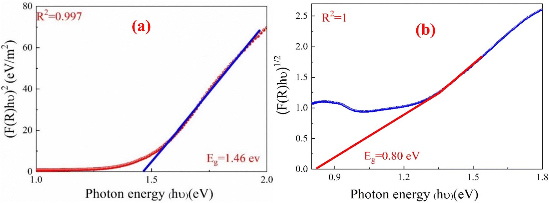 | ||
| Fig. 5 (a) (F(R)hν)2 spectra versus the photon energy (hν) for direct band gap energy.21 (b) (F(R)hν)1/2 spectra versus the photon energy (hν) for indirect band gap energy for the eco-friendly CFO nanoparticles. | ||
Crystalline materials invariably contain defect states. These defects create localized states within the energy bandgap, trapping excited electrons and preventing their direct transition to the conduction band.47 Nanoparticles, especially smaller ones, have a higher ratio of surface-to-volume atoms. The unsaturated bonds on a nanoparticle's surface induce stress in the atoms, leading to significant oxygen vacancies, cation defects, and other crystalline imperfections. These defects and oxygen and cation vacancies act as exciton-trapping centers within the energy band gap. They form a series of metastable energy levels that hinder charge carriers from transitioning into the conduction band.48
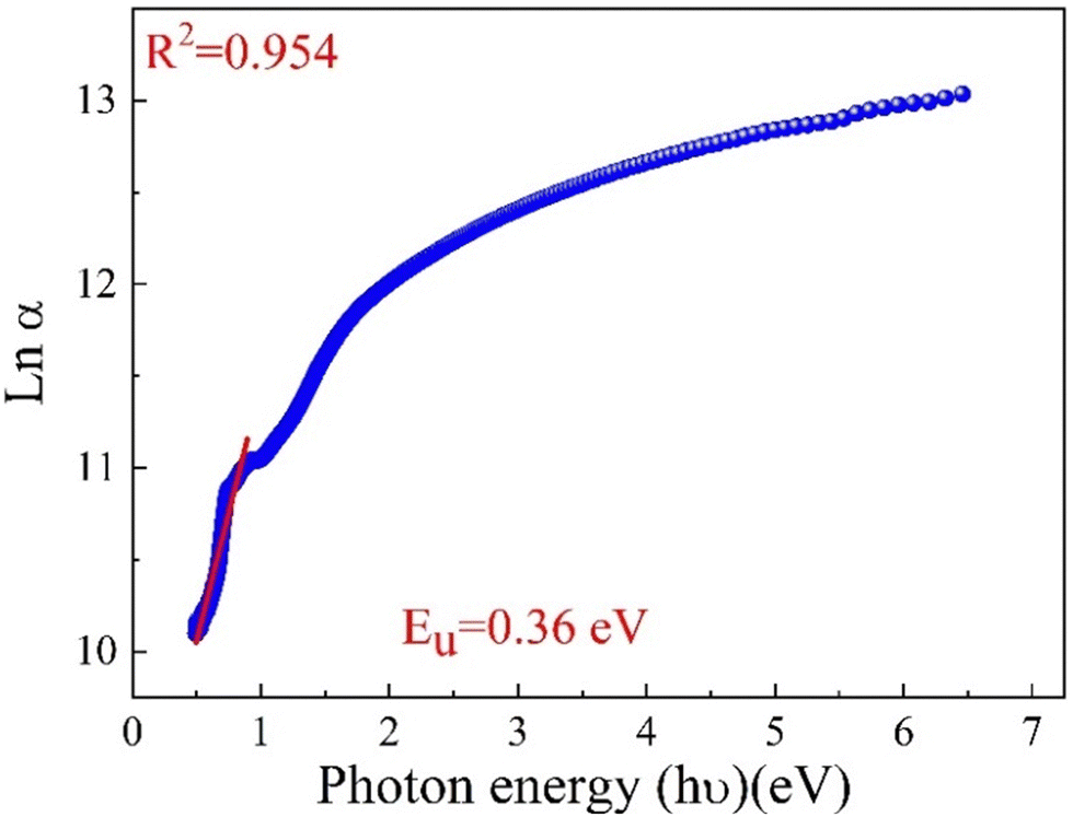
Urbach energy is an optical parameter representing the defect states in the optical band gap region. These localized defect states in the band gap region cause the formation of an absorption tail in the absorption spectrum, known as the Urbach tail. Urbach energy refers to the energy associated with this tail.47 The absorption spectra can be used to determine Urbach energy, which can be calculated using eqn (S11) and (S12) (ESI†). The Urbach energy (Eu) can be determined from the absorption spectra. To estimate the value of Eu, a plot of ln(α) versus photon energy is used (Fig. 6). Eu is derived from the reciprocal of the slope obtained by fitting the linear portion of this plot.47 The synthesized CFO sample exhibits an Urbach energy of approximately 360 meV. This moderate value indicates a considerable amount of structural disorder within the sample, likely due to surface dangling bonds that create a high density of localized defect states in the band gap region.48
 | ||
| Fig. 6 Urbach energy plot of the eco-friendly CFO nanoparticles. | ||
The steepness parameter S(T) can be estimated using eqn (S13) (ESI†). The value of S at ambient temperature for the eco-friendly synthesized CFO sample was determined to be 0.067. Additionally, the steepness parameter is inverse to the electron–phonon interaction Ee–ph (eqn (S14), ESI†). The estimated Ee–ph value, based on eqn (S14) (ESI†), was found to be 10 eV. The maximum wavelength (λT) of the incident light is crucial in determining the suitability of a substance for optoelectronic devices, as it indicates the minimum wavelength needed for charge carrier expulsion. The value of (λT) can be calculated using eqn (S15) (ESI†). The threshold wavelength (λT) was determined to be 432.33 nm by plotting (Fig. 7).
 | ||
Fig. 7 Variation of  as a function of as a function of  to estimate the threshold wavelength (λT). to estimate the threshold wavelength (λT). | ||
When a substance interacts with light, it absorbs specific wavelengths, reducing the flow of incoming photons. To understand the extent to which the compound allows incident radiation to penetrate, we can use the concept of penetration depth or skin depth (δ), “it is the depth at which the intensity of the incident photon decreases to 1/e of its initial incident value”.49 The calculation of (δ) is based on the relationship that defines the α(λ) curve (eqn (S16), ESI†). The penetration depth (δ) vs. (λ) curve of the eco-friendly CFO sample synthesized via the green method exhibits three distinct zones (Fig. 8). In the first part of the spectrum (region I), the sample shows complete absorption of UV radiation, indicating its potential as an effective UV filter.50 Moving into the second region (region II), δ(λ) increases, reaching its peak at λ = 1108 and 1575 nm. In the third region (region III), the δ(λ) values rise progressively, reaching 2400 nm. In the ultraviolet (UV) region, the penetration depth remains very low, indicating that the material absorbs most of the incident photons. This behavior is attributed to the high absorption coefficient α of the material in this range, where electronic transitions from the valence band to the conduction band are dominant. These transitions are primarily driven by ligand-to-metal charge transfer (O 2p → Fe 3d and Co 3d states), as supported by the UV-Vis absorption spectrum. The steep decrease in penetration depth in this region confirms the strong interaction between the incident photons and the electronic states of the material. As the wavelength increases into the visible and near-infrared (NIR) region, the penetration depth increases gradually due to the decrease in the absorption coefficient. In this range, the material exhibits lower photon absorption as d–d electronic transitions (crystal field transitions of Fe3+ and Co2+ ions in octahedral and tetrahedral sites) become dominant. These transitions have lower oscillator strengths, resulting in reduced absorption and a corresponding increase in penetration depth. In the far-infrared region, the penetration depth increases significantly, indicating minimal absorption. This trend suggests that the dominant absorption mechanisms (electronic transitions and defect-mediated absorption) become weaker at longer wavelengths, and the material becomes more transparent to the incident photons. The increase in penetration depth in this range is also influenced by phonon interactions and free-carrier absorption, which have weaker contributions compared to electronic transitions. Additionally, the penetration depth curve aligns with the extinction coefficient (k) trend, confirming the fundamental relationship between optical absorption and penetration depth.
 | ||
| Fig. 8 Variation of penetration depth (δ) as a function of the incident photon wavelength (λ). | ||
Furthermore, the extinction coefficient k, representing the attenuation of an electromagnetic wave within a medium, can be calculated using eqn (S17) (ESI†). Fig. 9 shows the extinction coefficient k curve of the synthesized CFO sample plotted against photon energy hν. In the range of hν = 0.4 to 0.7 eV, there is a noticeable increase in the k coefficient with rising photon energy. However, the K values sharply decline until hν = 1.1 eV. It is observed that the k values progressively increase with an increase in photon energy, followed by a gradual decrease. The observed increase in the extinction coefficient k can be attributed to the enhanced ability of the prepared sample to reflect incident photons in this energy range. Conversely, the observed decrease in K can be attributed to the reduction in incident photon energy near the illuminated surface. Similar phenomena have been observed in other spinel materials as the photon energy increases.51,52
 | ||
| Fig. 9 Variation of the extinction coefficient (k) as a function of the incident photon energy (hν). | ||
The refractive index n is a fundamental optical parameter of any material when exposed to light. It is essential for characterizing spectral dispersion and assessing a material's optical responsiveness for various applications. The refractive index n can be determined using eqn (S18) (ESI†). Fig. 10(a) displays the variation in the refractive index (n) of the synthesized CFO sample as a function of wavelength (n(λ)). The refractive index of the material exhibits significant dependence on the wavelength. The spectrum's UV, visible, and near-infrared (NIR) regions reveal prominent absorption bands, highlighting the exceptional quality and compactness of the synthesized sample. These absorption features are depicted in the (n(λ)) curve. To further characterize the (n(λ)) curve, the Cauchy parameters n0, n1, and n2 can be employed, as detailed in eqn (S19) (ESI†). The refractive index can be determined using Cauchy analysis for materials with weak absorption. The n versus 1/λ2 curve, modeled by eqn (S19) (ESI†), is shown in Fig. 10(b). The Cauchy parameters for the sample were obtained from the fitting curve: n0 = 1.80 ± 0.005, n1 = 0.016 ± 0.00096 (μm2), and n2 = 9.66 × 10⁻⁴ ± 4.2 × 10⁻⁵ (μm4).
 | ||
| Fig. 10 (a) Variation of refractive index (n) as a function of the incident photon wavelength (λ). (b) Variation of (n(λ)) with Cauchy fit. (c) The Plot of 1/(n2 − 1) versus (hν)2 (d) plot of 1/(n2 − 1) versus 1/λ2 for the green-synthesized CFO nanoparticles. | ||
The Wemple–DiDomenico relationship was also used to determine the dispersion energy Ed and the energy of the effective single oscillator E0 (eqn (S20), ESI†). By fitting a linear segment to the curve of 1/(n2 − 1) versus (hν)2, as shown in Fig. 10(c), we can ascertain the E0 and Ed values for the prepared CFO sample. The slope of the linear portion is equal to 1/E0Ed, while the vertical intercept is related to E0/Ed. Based on this analysis, the values for E0 and Ed were calculated to be 1.16 ± 0.01 eV and 3.08 ± 0.02 eV, respectively. Additionally, with these data, we can estimate the static refractive index  and the optical dielectric constant εop at zero frequency using eqn (S21) (ESI†). This calculation yielded values of 1.92 and 2.66 for
  and εop. The computed value for
  closely matches the value obtained from the Cauchy fit. To calculate the average oscillator wavelength λ0 and oscillator strength S0, eqn (S22) (ESI†) was used.
The 1/(n2 − 1) curve versus 1/λ2 is plotted in Fig. 10(d). After performing a linear fit to the curve, the values for S0 and λ0 were determined to be 3.64 × 10⁻⁴ nm−2 and 1174.62 nm, respectively.
Inter-band transition intensities can be assessed using the moments of the optical spectrum M−1 and M−3. These moments were calculated using eqn (S23) and (S24) (ESI†). The calculations gave values of 2.66 and 1.99 for M−1 and M−3, respectively. These moments are indicative of the average bond strength. eqn (S23) and (S24) (ESI†) represent a single-oscillator approximation of the dielectric response for the prepared sample. The optical moments are linked to macroscopic quantities, such as the effective dielectric constant and the adequate number of valence electrons in the material under investigation.53 Table S3 (ESI†) summarises all estimated optical parameters, including Eg, EU, Ee–ph, E0, Ed, Cauchy's parameters, M−1, and M−3.
Fig. 11(a) shows the variation in optical conductivity (σop) for the prepared CFO sample as a function of wavelength (λ), based on eqn (S25) (ESI†). The optical conductivity (σop) measures a material's ability to conduct electromagnetic radiation and indicates its response to oscillating electromagnetic fields at optical frequencies.54 Higher values are observed at shorter wavelengths, while lower values occur at longer wavelengths in the optical frequency range. The significant optical conductivity at shorter wavelengths can be attributed to the excitation of electrons by high-energy photons, resulting in a robust photo-response of the sample.
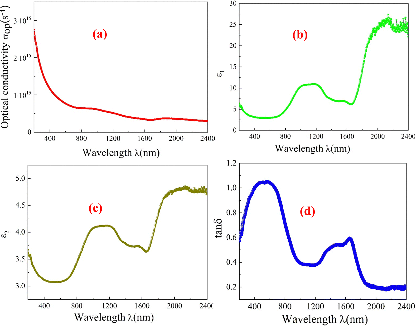 | ||
| Fig. 11 (a) Optical conductivity as a finction of wavelength (λ) (b) real part of the optical dielectric permittivity ε1 as a function of wavelength (λ) (c) imaginary part of the optical dielectric permittivity ε2 as a function of wavelength (λ) (d) optical loss factor tan (δ) as a function of wavelength (λ) for the green-syenthesized CFO nanoparticles. | ||
Furthermore, the efficiency of a material's interaction with an electric or electromagnetic field can be determined by measuring its optical dielectric permittivity. To calculate the complex dielectric permittivity, eqn (S26) (ESI†) was used. For applications in optoelectronic devices, various theoretical models have been developed to analyze dielectric constants, which characterize the optical properties of a solid material. The real part (ε1) of the dielectric constant indicates how much it slows down the speed of light within the material, while the imaginary part (ε2) represents the absorption of radiation by free carriers within the material.55
Eqn (S26) (ESI†) represents the real ε1 and imaginary ε2 components of the optical dielectric permittivity, which can be expressed using eqn (S27) and (S28) (ESI†). Fig. 11(b) and (c) show the graphs of ε1(λ) and ε2(λ). The ε1(λ) plot exhibits similar behaviour to the n(λ) curve due to the low extinction coefficient k(λ). In contrast, the imaginary part ε2(λ) depends mainly on the extinction coefficient k(λ). It is observed that the imaginary part exhibits low values compared to the real part, which clarifies the low energy loss of light traveling through the compound.
Additionally, examining the real and imaginary parts of the dielectric constant provides insights into the optical loss factor tan(δ), which is defined as the ratio of the imaginary part to the real part of the dielectric constant.56 The relationship between the optical loss factor, tan(δ), and λ is shown graphically in Fig. 11(d).
The redox potentials of the reaction must lie between the valence and conduction band potentials of the semiconductor for the application to be thermodynamically feasible.
The band edges of the conduction band (CB) and valence band (VB) can be estimated using the Mulliken electronegativity rules concerning the normal hydrogen electrode (NHE) scale at pH = 0, using eqn (S29) and (S30) (ESI†).
The absolute electronegativity of the prepared CFO sample, also known as Millikan electronegativity (χ), can be calculated using eqn (S31) (ESI†). The sample's absolute electronegativity (χ) is around 5.81 eV, calculated using the electron affinity and first ionization energy values from the periodic table for oxygen, cobalt, and iron atoms. Table S3 (ESI†) lists the sample's valence band edge (EVB) and conduction band edge (ECB) values.
3.3. Electrical properties (dielectric measurements)
Fig. 12(a)–(c) display the frequency dependence of AC conductivity for the prepared sample in the low-, intermediate-, and high-temperature regions, respectively. The conductivity spectra across these temperature ranges exhibit the following features, which will be discussed briefly:
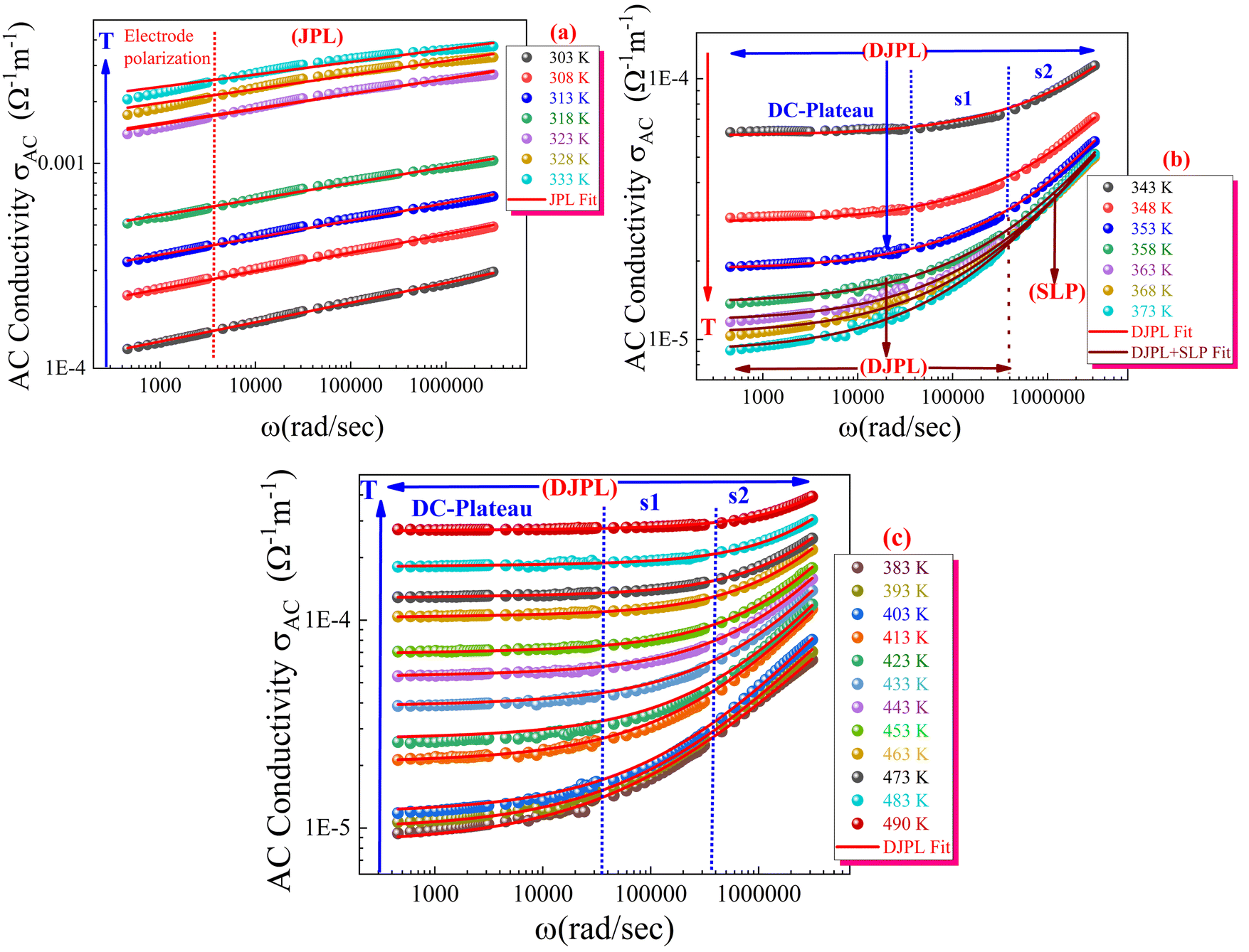 | ||
| Fig. 12 Double logarithmic plots of frequency-dependent conductivity spectra for the green-synthesized CFO nanoparticles across different temperature ranges: (a) 303–333 K, (b) 343–373 K, and (c) 383–493 K. The various symbols represent experimental data points, while the continuous lines correspond to the best non-linear fits for the different models applied. | ||
1. The frequency dependence of AC conductivity can be categorized into four, three, two, or even one region, depending on the temperature range and associated conduction mechanisms.
2. Johnscher's power law could not be consistently applied across the entire frequency range (100–106 Hz) or for all the tested temperatures (303–493 K).
3. The AC conductivity behaviour varies with temperature. It increases between 303 K and 333 K, decreases from 343 K to 373 °C, and then increases again between 383 K and 490 K.
4. A significant decrease in conductivity is observed in the very low-frequency range of 100–103 Hz (Fig. 12(b)), which is attributed to ion blockage at the interface between the electrode and the sample, known as electrode polarization.
5. The conductivity appears almost independent of frequency in the low-frequency range. It is comparable to the bulk conductivity (in the plateau region), called DC conductivity (Fig. 12(b) and (c)).
6. In the high-frequency region, the power law behaviour is observed with the expression σac = Aωs (Johnscher's Power Law, JPL) (Fig. 12(a)). Additionally, the formulas σac = Aωs1 + Bωs2 (Double Johnscher's Power Law, DJPL) and σac = Aωs1 + Bωs2 + Bωs3 (Double Johnscher's Power Law with Super Linear Power Law, DJPL + SLP) are noted (Fig. 12(b)). Moreover, σac = Aωs1 + Bωs2 (Double Johnscher's Power Law, DJPL) is also represented in Fig. 12(c).
7. AC conductivity's power law behaviour is dependent on temperature, similar to DC conductivity over the whole temperature range.
The variation in the AC conductivity behaviour with temperature can be explained as follows:
Conduction in ferrites typically occurs through a temperature-dependent hopping process.57 Cobalt and iron atoms generally occupy the A- and B-sites in a mixed spinel structure. The conductivity type is determined by interactions between cations (c–c) and cations and anions (c–a–c) at the B-site. Metallic-like (Insulating) conduction (where AC conductivity decreases with temperature) occurs when the cation–cation (Fe–Fe) interaction dominates, while semiconducting behaviour (where AC conductivity increases with temperature) is seen when the cation–anion–cation (Fe–O–Fe/Co–O–Co) interaction prevails.58 Two distinct transition temperatures have been observed: the first, at 343 K, corresponds to a semiconductor-to-metal transition, while the second, at 383 K, represents an insulator-to-semiconductor transition. These transitions are influenced by various thermal effects on the material's electronic structure, charge carrier dynamics, and defect states. Here are the suggested key reasons for these transitions:
a. Semiconducting behaviour near room temperature (303–333 K). At temperatures near room temperature, CFO exhibits semiconducting behaviour, where charge carriers are thermally activated and can move through the conduction band or hop between localized states. As the temperature increases, more carriers gain energy to contribute to conduction, leading to increased conductivity.
b. Semiconducting–insulator transition in the intermediate temperature range (343–373 K). In the intermediate temperature range (343–373 K), CFO undergoes a semiconductor-to-insulator transition characterized by a temporary decrease in conductivity. This behaviour arises from several factors: charge carrier trapping in defect states or localized sites reduces the number of free carriers available for conduction; thermal expansion alters grain boundary resistance, creating barriers that lower conductivity; temperature-dependent dielectric relaxation can store energy, diminishing current flow; increased phonon interactions scatter charge carriers more frequently, reducing their mobility; and a shift in conduction mechanisms from hopping to quantum mechanical tunnelling further contributes to the observed decrease in conductivity; the synthesized CFO ferrite sample with a mixed spinel structure primarily has Fe3+ ions occupying edge-sharing octahedral sites, unlike typical CFO, where Co2+ ions partially fill these sites. This unique arrangement enhances strong, long-range cation interactions within the octahedral sublattice. The delocalized electrons facilitate efficient movement, leading to metallic-like thermal behaviour characterized by decreasing conductivity with increasing temperature.59 Together, these effects give the material a metallic-like behaviour in this temperature range.
c. Insulating–semiconducting transition in high-temperature range (383–493 K). In the high-temperature range (383–493 K), CFO experiences a transition from insulating back to semiconducting behaviour, leading to increased conductivity. This shift is primarily due to the activation of defect states, where trapped carriers gain enough energy to re-enter the conduction process. Additionally, lattice expansion at elevated temperatures narrows the band gap, increasing the carrier concentration and contributing to semiconducting behaviour. The thermal excitation of charge carriers also becomes more significant at higher temperatures, further boosting conductivity as more carriers are activated across the band gap. These combined effects return the material to semiconducting behaviour in this temperature range.
In the first temperature region (303–333 K) (Fig. 12(a)), the curves are closely spaced near room temperature and converge as temperature increases, indicating that the conductivity of the prepared sample has low-temperature dependence60 in this range (323–333 K). The conductivity behaviour shows a linear relationship (one region) with the frequency of the applied electric field without a distinct plateau, which suggests very low DC conductivity. Additionally, the green-synthesized CFO material demonstrates semiconducting behaviour, where conductivity increases with temperature. In this region, the total conductivity is the sum of both DC and AC components. To analyze the frequency-dependent conductivity, the universal Jonscher's power law is applied (eqn (S33), ESI†). The AC conductivity follows a power law behaviour in terms of angular frequency ω, where A is a temperature-dependent constant (a pre-exponential factor that can estimate the strength of the polarizability),61 and s is an exponent that reflects the degree to which ions interact with their environment. This exponent provides critical insights into the conduction mechanism of the material, offering valuable information about how ions move and the material's electrical behaviour.62
Moreover, in the low-frequency region, electrode polarization dominates the conduction process. As the frequency of the applied electric field increases, the interaction between charge carriers intensifies, leading to a rise in the AC conductivity value (Fig. 12(a)). This behaviour indicates that the influence of polarization diminishes at higher frequencies, allowing charge carriers to move more freely, which enhances conductivity. Fig. 12(a) shows the frequency-dependent fitting of AC electrical conductivity for eco-friendly CFO, using Jonscher's law. The solid red line in the figure closely aligns with the experimental data, demonstrating that the conductivity model fits well with the observed values. The conductivity parameters, including Sigma dc, s, and A, are summarized in Table S4 (ESI†).
According to Funke's criteria,63 when the exponent s > 1, it indicates localized hopping between neighboring sites (re-orientational motion along with well-localized ions); for well-localized ions, the hopping motion occurs only in the vicinity of the ion's original position, meaning that the ion remains close to its initial site. In contrast, during re-orientational motion, the dipole aligns itself in response to the external electric field, adjusting its orientation without significant displacement from its original position,64 while s < 1 suggests abrupt translational hopping. Fig. 13(a) shows a gradual decrease in the frequency exponent s as the temperature increases and that its values are all less than 1, indicating that the conduction primarily follows the correlated barrier hopping (CBH) model.65 This model proposes that charge transport occurs via a single or bipolaron hopping mechanism across a Coulomb barrier between two trapping centers. In this context, the frequency exponent s is mathematically expressed within the CBH model using eqn (S34) and (S35) (ESI†), which reflect the nature of the hopping mechanism and charge transport across the material. The lowest value of the frequency exponent s observed at 333 K suggests a significant interaction between the charge carriers and the lattice vibration. This strong interaction indicates that the hopping mechanism of the charge carriers is greatly influenced by the surrounding lattice, which may hinder their movement and contribute to the observed conductivity behaviour in the second temperature region (343–373 K).
 | ||
| Fig. 13 (a) Temperature variation of the exponents “s” and “1 – s” within the temperature range of 303–333 K (b) Plot of ln(σdcT) as a function of (1000/T) within the temperature range of 303–490 K for the eco-friendly synthesized CFO nanoparticles. | ||
The slope of the (1 – s) versus temperature curve for the prepared CFO sample (Fig. 13(a)) was used to calculate the Wm value. The calculated Wm value is 472 meV. Bipolaron hopping is the dominant conduction mechanism when the maximum barrier height WM is equal to half the activation energy (Ea/2), whereas single polaron hopping dominates when WM is approximately one-fourth of the activation energy (Ea/4).66 From the analysis of the DC conductivity fits using the correlated barrier hopping (CBH) model (Fig. 13(b)-(I)), it was determined that Wm is approximately half the activation energy, suggesting that bipolaron hopping is the primary conduction mechanism in the prepared CFO sample. This behaviour indicates that the hopping mechanism is the dominant process in the material's conduction and confirms the thermal activation of charge carriers.
Additionally, the behaviour of DC conductivity (extracted from the fitting of AC conductivity using Johnscher's equation) is well-described by the Arrhenius relation, given by eqn (S36) (ESI†). In Fig. 13(b), eqn (S36) (ESI†) was used to calculate the activation energy Ea for the prepared sample, represented as a plot of ln(σdcT) versus (1000/T). The value of Ea is determined from the linear fitting of this curve, and it is about 0.975 eV for the first temperature region, which is smaller than those observed for other spinel ferrite materials.61,67,68 M. Idrees noted that activation energies up to 200 meV typically indicate electron hopping, suggesting a relatively low energy barrier for charge transport.69 On the other hand, D. Bouokkeze66 and colleagues emphasized that higher activation energies, often in the range of several hundred meV (500–1300 meV), could stem from multiple contributing factors, necessitating a deeper investigation into the underlying physics. These factors may include electron hopping within ferromagnetic intra-grains70 and the simultaneous presence of other complex mechanisms affecting conductivity.71
Moreover, for the simplified (CBH) model, the alternating current (AC) conductivity and the hoping distance Rω under the condition of ωτ = 1 were defined by eqn (S37) and (S38) (ESI†). In the Correlated Barrier Hopping (CBH) model (pair model), conduction is influenced by electrons “skipping” between two defect centers, separated by a Coulomb barrier that isolates them. The model was originally introduced by Pike72 in 1972 to describe the hopping of a single electron. Later, in 1977, Elliot73 expanded the model to include the simultaneous hopping of two electrons. The barrier height between defect centers is determined by the distance separating them, with Coulomb interactions playing a key role. When defect sites are closer together (a small separation Rω), the potential wells begin to overlap, which causes a reduction in the barrier height from Wm to Wh, as depicted in Fig. 14.
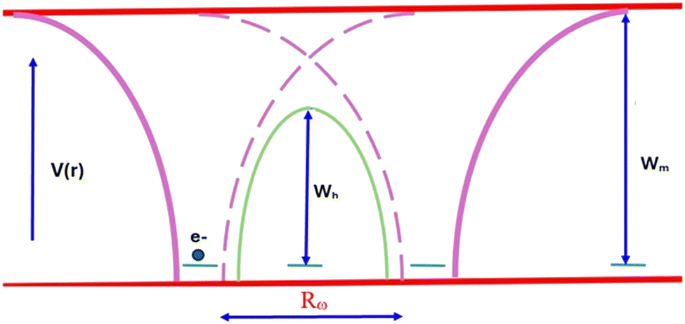 | ||
| Fig. 14 Illustration of the Coulomb barrier of the pair model (CBH) model. | ||
Fig. 15 illustrates the temperature dependence of Rω (the hopping distance) at various frequencies, showing how the hopping distance evolves with temperature across different applied electric fields. As the temperature rises, the hopping length decreases. This phenomenon can be explained by increased thermal energy enhancing the ability of charge carriers (such as electrons or holes) to hop between localized states more easily. However, the accompanying thermal agitation causes a reduction in effective hopping distance due to increased scattering with phonons and lattice defects. As temperature increases, the motion of the carriers becomes less coherent, disrupting the lattice structure and reducing the hopping distance. Additionally, rising temperatures may generate more defects or vacancies within the material. These defects can trap charge carriers, limiting their mobility and reducing the average hopping length. Defects in the lattice also create localized states that hinder the hopping process, contributing to the reduced hopping length. On the other hand, the hopping distance increases with the frequency of the applied electric field, as shown in Fig. 14. At higher frequencies, charge carriers tend to align more effectively with the field, improving their mobility. This alignment helps carriers overcome energy barriers more efficiently, increasing the effective hopping length. Furthermore, the interaction time between the charge carriers and the lattice is reduced at higher frequencies. This reduced interaction minimizes scattering events, allowing longer hopping distances since the carriers are less likely to be trapped by lattice imperfections.
 | ||
| Fig. 15 Temperature-dependent variation of the hopping distance Rω at different frequencies for the eco-friendly synthesized CFO nanoparticles within the 303–333 K temperature range. | ||
In the second temperature region (Fig. 12(b)), three distinct frequency ranges emerge as the temperature rises between 343 and 353 K. Throughout the entire frequency spectrum, the behaviour of the conductivity follows a double Jonscher power law (DJPL),74,75 which features both a DC plateau (σdc) and a sub-linear dispersive region characterized by two different slopes (s1 and s2 which vary between 0 and 1). The double Jonscher variation indicates that multiple hopping and tunnelling conduction mechanisms occur simultaneously within the same temperature range in the material.76 At lower frequencies (100–104 Hz), the curves remain steady, which is attributed to the increased influence of the grain boundary effect.77 This aligns with the DC conductivity plateau and suggests long-range transport of charge carriers in response to the applied external electric field.78 At these low frequencies, the magnitude of the field is insufficient to induce significant hopping conduction, thereby limiting charge carrier movement and keeping conductivity constant.78 It has been observed that the range of DC conductivity remains unchanged mainly with increasing temperature. This may suggest that charge carriers move within the same time frame, regardless of temperature fluctuations. Consequently, their mobility decreases, reflected in a reduced conductivity at low frequencies under the influence of temperature. This behaviour highlights the limited effect of thermal energy on the carriers’ ability to enhance conductivity in this frequency range (thermally deactivated electrical conductivity “metallic-like behaviour”). The second region of conductivity >104 Hz, which increases with frequency, corresponds to the AC conductivity. The exponential increase in conductivity within the AC regime is associated with the behaviour of conductive grains at higher frequencies.79 This suggests that charge carriers are more likely to hop between these conductive granules at elevated frequencies, leading to a sharp rise in conductivity. The double Jonscher power law (DJPL) variation can be analyzed using the Bruce model (eqn (S39), ESI†). Moreover, a transition from a double Jonscher power law (DJPL) with sub-linear behaviour to a superlinear power law (SPL) behaviour is observed at frequencies around f = 105 Hz, particularly as the temperature increases from 358 to 373 K (Fig. 12(b)). In this context, the conductivity spectra can be divided into four frequency regions (three frequency regions for DJPL and one for SPL), with the SPL behaviour becoming dominant in the higher frequency range. In the SPL frequency range, conductivity remains unaffected by temperature changes, suggesting that the SPL contribution is thermally inactive80–91 with frequency exponent exceeding the “unity”. Studies show that SPL behaviour can be observed at low temperatures and within the same frequency range, maintaining a consistent frequency exponent.80–91 This type of behaviour has been extensively reported and characterized across various material systems.80–91 According to Avogadro et al.,80 this behaviour can be attributed to the presence of two-level systems. Dieckhöfer et al.85 further explained the emergence of the SPL regime as being caused by low-energy vibrational excitation modes. Elliott92 proposed that the appearance of SPL behaviour might result from a particular spatial distribution of charged fault centres, likely due to the Coulomb interaction between centres of opposite charge. Additionally, Stanguennec and Elliott86 suggested that the SPL regime arises from local ion hopping in an asymmetrical double-well potential, with a reduction in the dispersion of barrier heights. Our data related to the SPL model (according to Stanguennec and Elliott) in this temperature range may confirm the presence of two barrier heights (asymmetric double-well potential) in the third temperature region. The equation below describes the total conductivity spectra σT(ω) in the temperature range of 358–373 K across the studied frequency band.
| σT(ω) = DJPL + SPL = σdc + A1(T)ωs1(T) + A2(T)ωs2(T) + B3(T)ωs3(T) | (1) |
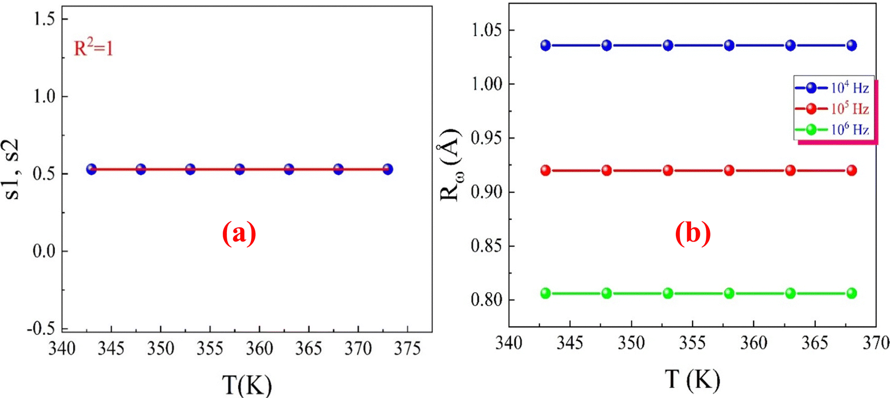 | ||
| Fig. 16 (a) Temperature variation of the exponents “s”. (b) Thermal variation of the tunnelling distance Rω as a function of the frequency of the applied electric field for the eco-friendly synthesized CFO nanoparticles within the temperature range of 343–373 K. | ||
In the third temperature region (Fig. 12(c)), the temperature dependence of the AC conductivity, as a function of the frequency of the applied electric field, follows a double Jonscher power law (DJPL) within the range of 383–493 K. In this temperature region, the prepared CFO material exhibits semiconducting behaviour, where conductivity increases with temperature. The Bruce model can give the total conductivity of the prepared CFO ferrite sample in this temperature region, which can be expressed using eqn (S39) (ESI†).
Additionally, we identified the primary conduction mechanism in our ferrite material by analyzing the fluctuation of the exponent s with temperature (Fig. 17). The observed increase in s1 and s2 values with rising temperature suggests a thermally activated process. Our findings indicate that the nonoverlap small polaron tunnelling (NSPT) model94 accurately describes the conduction mechanism in the third temperature region.
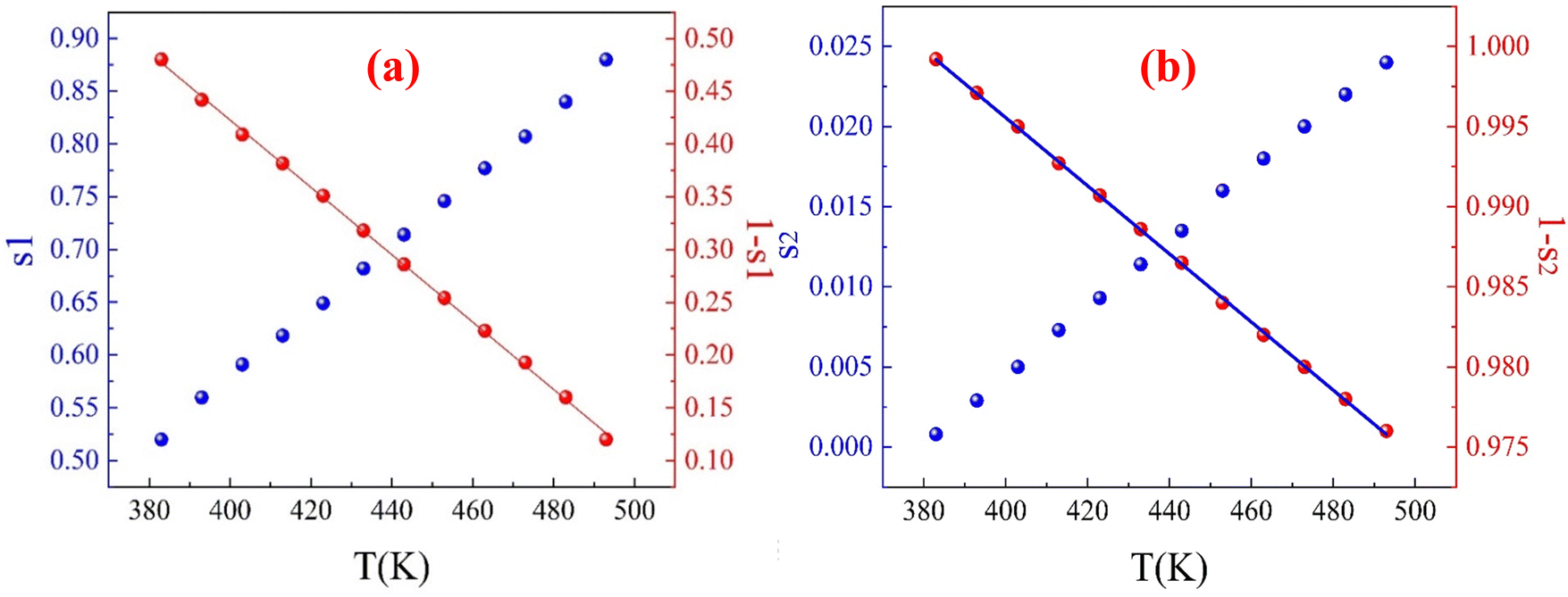 | ||
| Fig. 17 (a) Temperature variation of (a) the exponents “s1” and ”1 – s1” and (b) the exponents “s2” and “1 – s2” for the eco-friendly synthesized CFO nanoparticles within the temperature range of 383–393 K. | ||
The Coulomb interaction between conduction electrons and lattice ionic charge carriers creates a quasi-particle, resulting in strong electron–phonon coupling. Conduction electrons are surrounded by virtual phonons, which attract positive ions and repel negative ones. Polarons, quasi-composite particles formed by electrons and virtual phonons, polarize the system by altering its energy state configuration. In a polarizable continuum medium, the electron's mobility and effective mass can be estimated, leading to the classification of polarons as either large or small.62 Thermally induced hopping forms a small polaron by distorting charge carriers and causing ionic displacement, confined to a volume of one unit cell or less, typically between nearest neighbours.62
The exponent s can be determined using the NSPT model through eqn (S42) and (S43) (ESI†). According to eqn (S43) (ESI†) produced a linear fit for the (1 – s1) and (1 – s2) data (indicated by the red and blue solid lines in Fig. 17(a) and (b)), which yielded Wm values of approximately 0.11 eV and 1.67 eV. The complex AC conductivity behaviour of CFO in the third temperature region arises from a dynamic interplay of microstructural, chemical, and thermal factors alongside electron–phonon interactions. Variations in local electronic structures and ionic distributions lead to differing polaron activation energies, enabling regions of both high and low barrier heights. Defects, grain boundaries, and chemical inhomogeneities further create localized conductivity variations by altering energy barriers for polaron hopping. Temperature influences this behaviour, as higher energies allow polarons to overcome larger barriers, while smaller barriers enhance mobility at lower energies. Additionally, variations in electron-lattice coupling result in regions with strong coupling that lower barriers through lattice assistance and weak coupling that relies on electronic tunnelling. This duality reflects a transition between adiabatic and nonadiabatic polaron tunnelling, where different conduction regimes dominate depending on the interaction strength. These factors contribute to the observed increase in AC conductivity and the coexistence of high and low barrier heights.
In summary, the AC conductivity of CoFe2O4 is influenced by a complex mixture of localized electronic structures, defects, thermal dynamics, chemical compositions, and electron–phonon interactions. These factors create a landscape where polarons can exhibit varied mobility, leading to the observed differences in polaron tunnelling behaviours and the overall electrical properties of the material.
Furthermore, Fig. 18 illustrates the Arrhenius relationship, which accurately describes the DC conductivity behaviour in the third temperature region, as outlined in eqn (S36) (ESI†). The estimated Edc values obtained from the linear fit of the curve are approximately 876 and 965 meV, which confirms the complex conduction mechanism in this temperature region.
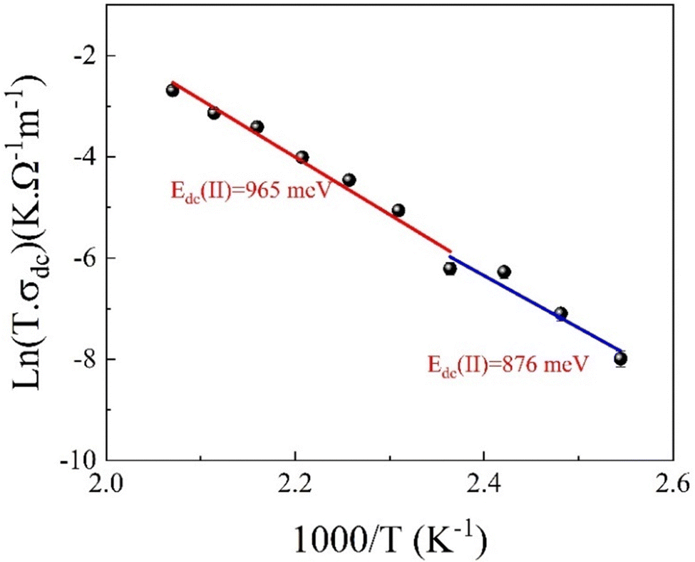 | ||
| Fig. 18 Plot of ln(σdcT) as a function of (1000/T) for the eco-friendly synthesized CFO nanoparticles within the 383–393 K temperature range. | ||
Moreover, based on the NSPT model, the AC conductivity and the tunnelling distance Rω can be described by eqn (S44) and (S45) (ESI†). These equations were used to calculate the fitting parameters, presented in Fig. 19(a), (b) and summarized in Table S5 (ESI†).
 | ||
| Fig. 19 Temperature dependence of the NSPT fitting model for the AC conductivity of green-synthesized CFO nanoparticles in the temperature range of (a) 383 to 423 K (b) 423 to 493 K. | ||
These results indicate that the charge transport mechanism in the prepared CFO ferrite sample in the third temperature region is primarily governed by site hopping, as evidenced by the high values of N(EF), which exceed 1038 eV−1 m−1. Additionally, the moderate values of polaron hopping energy (Wh), even at higher frequencies, suggest that the polaron hopping in this compound requires a moderate amount of energy to enable the transition from one site to another, which decreases as the frequency of the applied field increases. As shown in Table S5 (ESI†), both α and N(EF) increase with frequency. Since the number of charge carriers is proportional to N(EF), the observed increase in N(EF) with frequency confirms the enhancement of σ′ (ω) with frequency,95 as the thermal energy given to the sample in this temperature region is sufficient to liberate the trapped charge carriers. It is also observed that the hopping energy for the second temperature range (423–493 K) is higher than that of the first temperature range, which can be attributed to the higher barrier height value of this temperature region, as discussed in the previous section.
Fig. 20(a) and (b) illustrate the variations in Rω with frequency and temperature. Rω increases with temperature (in the whole temperature range), and it also increases/decreases with decreasing/increasing the frequency of the applied electric field in the first (383–413 K)/second (423–493 K) temperature range. At higher frequencies, the applied electric field oscillates more rapidly, which may assist the tunnelling process and increase the effective tunnelling distance (Fig. 20(a)) (strong electron–phonon coupling). The higher frequency field may also create dynamic polarization effects or resonant conditions that enhance tunnelling probability, thereby extending the tunnelling distance. Additionally, higher frequencies could lead to a higher energy state of the system, enabling carriers to penetrate through the barrier more efficiently, resulting in an increased tunnelling distance (in the first temperature region (383–413 K). The more rapid decline of Rω with frequency (Fig. 20(b)) indicates a transition of charge carriers from long-range to short-range tunnelling96 (weak electron–phonon coupling). This phenomenon is associated with the frequency-dependent enhancement of N(EF). Additionally, the increase in charge carrier mobility with rising temperature correlates with the observed increase in Rω the nature of the hopping mechanism as the temperature rises due to thermal excitation, which allows charge carriers to overcome the potential barriers more efficiently, effectively leading to a longer average tunnelling length (Fig. 20(a) and (b)).
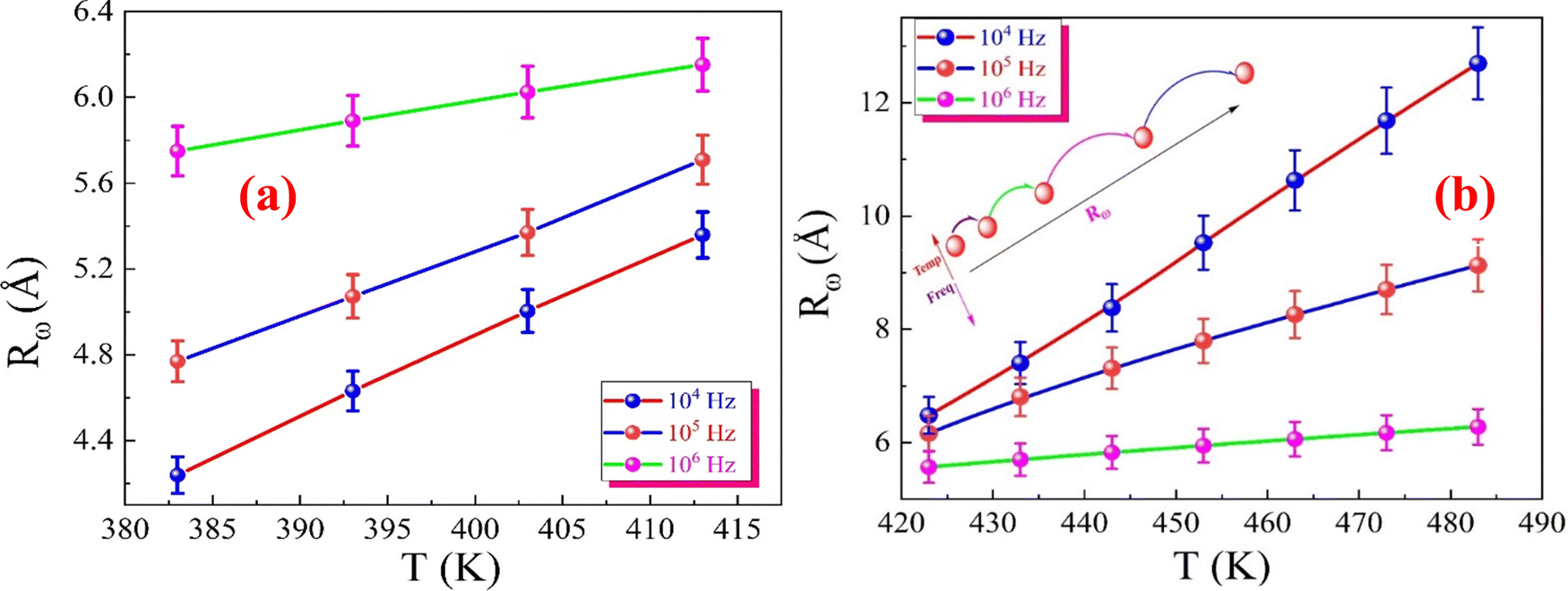 | ||
| Fig. 20 Temperature-dependent variation of the tunnelling distance Rω at different frequencies for the eco-friendly synthesized CFO nanoparticles within the temperature range of (a) 383–413 K and (b) 423–493 K. | ||
Fig. 21(a) presents the ln(σac) versus 1000/T curves for the prepared CFO nanoparticles at different applied field frequencies. Fig. 21(b) and (c) show magnified views of the linear fits in regions (I) and (III) at low and high temperatures for the same sample. The ln(σac) versus 1000/T curves exhibit an increasing trend in the first and third temperature regions, which indicates a smooth conduction process through the grain boundaries. Between these two regions, there is a sudden decrease in ln(σac) with increasing temperature, representing the insulating behaviour (metallic-like) of the sample in that temperature range. Due to the hopping of charge carriers, ferrites generally exhibit increased electrical conductivity as the temperature rises. Per the Maxwell–Wagner theory,61 the dielectric structure of ferrites consists of two components: well-conducting ferrite grains separated by thin, poorly conducting grain boundaries. These grain boundaries, typically composed of oxygen ions, are non-conducting and become active at low frequencies. This activity suppresses the hopping between Fe2+ and Fe3+ ions, leading to a decrease in hopping probability and, thus, a reduction in AC conductivity as the frequency decreases.61 Conversely, when the frequency of the externally applied electric field increases, the conducting grains become active, promoting the hopping mechanism between Fe2+ and Fe3+ ions and increasing the hopping probability. The overall effect is a gradual increase in AC conductivity with increasing frequency.61 In our CFO nanoparticles, both cobalt (Co2+) and iron (Fe3+) ions are distributed across the A and tetrahedral B sites. To maintain charge neutrality, a portion of Fe3+ ions is converted into Fe2+ ions.97 This conversion results in a system that facilitates both electron and hole-hopping mechanisms. Specifically, electrical conduction in CFO occurs through electron hopping between Fe2+ and Fe3+ ions and through hole hopping between Co2+ and Co3+ ions located at the B sites.98
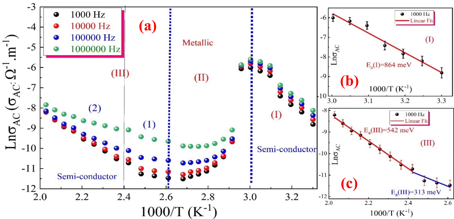 | ||
Fig. 21 (a) Variation of ln![[thin space (1/6-em)]](https://www.rsc.org/images/entities/char_2009.gif) σacversus 1000/T for the green synthesized CFO nanoparticles as a function of applied field frequencies, (b) and (c) show magnified views of the linear fits in regions (I) and (III) at low (303–333 K) and high (383–493 K) temperatures, respectively. σacversus 1000/T for the green synthesized CFO nanoparticles as a function of applied field frequencies, (b) and (c) show magnified views of the linear fits in regions (I) and (III) at low (303–333 K) and high (383–493 K) temperatures, respectively. | ||
The thermal activation of charge carriers contributing to the AC conductivity (σac) was further examined using the Arrhenius equation (eqn (S46), ESI†). The activation energy (Ea) was calculated for low and high-temperature regions across 1, 10, 100, and 1000 kHz frequencies. For each frequency, the emergence of distinct slopes in different temperature ranges indicates the existence of multiple conduction mechanisms (complex) with varying Ea values within the synthesized CFO sample. The estimated values of the activation energies at different temperature ranges and various frequencies are summarized in Table S6 (ESI†).
From Table S6 (ESI†), it can be observed that the estimated values of Ea(I) range from 0.864 eV at 1 kHz to 0.784 eV at 1000 kHz in the low-temperature region (Fig. 21(b)). The relatively high activation energy in this temperature range can be attributed to the following factors; at low temperatures, the thermally activated hopping of charge carriers, particularly bipolaron hopping between Fe2+ and Fe3+ ions at the octahedral sites within the ferrite structure, dominates the conduction mechanism, requiring thermal energy to overcome the localized energy barrier (0.472 eV). The activation energy represents the minimum energy required for electrons to transition between these ions, and since the temperature in this region is relatively low, many charge carriers remain trapped, necessitating additional energy input to facilitate mobility and contribute to electrical conductivity. In this low-temperature region, charge carriers are highly localized around specific ions due to the insufficient thermal energy required for hopping. The lack of thermal agitation makes it difficult for electrons to escape from their localized states, further increasing the activation energy required for conduction. As a result, hopping between Fe ions over long distances becomes challenging, further restricting charge transport. Additionally, in (CFO) ferrite, the presence of cation disorder (mixed spinel structure) and structural imperfections, such as vacancies and defects, introduces additional energy barriers for charge carrier movement. These barriers become more pronounced at low temperatures when charge carriers lack the necessary kinetic energy to overcome them, further increasing the observed activation energy and reflecting the extra effort required to transition from one localized state to another.
In the third temperature region (high-temperature), the values of the activation energy Ea(III) range from 0.222 eV to 0.313 eV in the first sub-region and from 0.290 eV to 0.542 eV in the second sub-region, as shown in Fig. 21(c). In this temperature region, the increased thermal energy leads to a shift in the conduction mechanism to a nonoverlapping small polaron tunnelling mechanism. This involves charge carriers (polarons) hopping between localized sites with lower activation energies than at lower temperatures. The activation energies are lower than that in the low-temperature region, indicating that less thermal energy is needed for conduction due to the increased concentration and mobility of charge carriers. According to Jonker,99 the induced lattice vibration facilitates the transfer of charge carriers between different sites, increasing the AC conductivity. Also, the presence of two ranges of activation energy (low and high) in this temperature region confirms the presence of two barrier heights. The small values of these activation energies propose that the conduction mechanism in this temperature region is due to charged defects conduction along a short-range hopping motion of oxygen vacancy ions100 (hopping of oxygen vacancies between different oxidation states of iron ions Fe2+and Fe3+) to random sites. These sites have different heights and various separating distances.101,102
An insulating behaviour is observed in the intermediate temperature region, characterized by a positive temperature coefficient of resistance (PTCR), where the AC conductivity decreases as the temperature increases. This is indicated by the presence of negative activation energy, reflecting the insulating nature of the sample in this temperature range. This behaviour can be attributed to magnetic transitions or scattering mechanisms, as CFO is a ferrimagnetic material in this range. Changes in magnetic ordering or spin alignment can impact the mobility of charge carriers, leading to reduced conductivity with increasing temperature. Additionally, increased electron–phonon or electron-magnon scattering at these temperatures can hinder the movement of charge carriers, resulting in the observed negative activation energies.
From Table S6 (ESI†), one can observe that the activation energy (Ea) decreases with increasing frequency of the applied electric field across all temperature ranges for the green synthesized CFO nanoparticles. It is well understood that the conduction mechanism involves a combination of hopping, mobility, and the transport of charge carriers within the sample. As the frequency increases, the hopping and transport mechanisms become restricted to the nearest neighboring defect centers due to the shorter time available for charge carriers to respond to the rapidly changing external field.103 This restriction leads to a decrease in Ea with increasing frequency in our sample.
 | ||
| Fig. 22 Variation of the real part of the permittivity ε′ with the angular frequencies (a) for the first temperature region (303–333 K), (b) for the second temperature region (343–373 K), and (c) for the third temperature region (383–493 K) for the synthesized CFO ferrite nanoparticles. The inset shows the H–N model fitting. | ||
The observations indicate that our ferrite sample exhibits a relaxation mechanism that deviates from the typical Debye type. The thermal dependence of dielectric dispersion and relaxation times are frequently observed in disordered solids or glass-forming composites. Additionally, these systems often display mixed dispersion and relaxation behaviours that deviate from Debye-type dynamics, commonly due to short-range atomic and polaron transport within and between clusters. Consequently, unlike the traditional Debye or Cole–Cole models, a dual formalism accounting for symmetric and asymmetric dispersion was developed to describe the complex permittivity response, which also varies with temperature. This approach is known as the Havriliak–Negami (H–N) model given by eqn (S47)–(S49) (ESI†). The experimental data presented in Fig. 22(a)–(c) was fitted to eqn (S47) (ESI†) using the best-fit method. The solid lines in the insets of Fig. 22(a)–(c) represent the optimized fits. The obtained values for εs and ε∞, and the shape parameters from these fits are summarized in Table S7 (ESI†).
A review of the dielectric parameter data for the first temperature region (Table S7, ESI†) reveals that both εs and ε∞ increase with rising temperature. This effect likely arises from thermally generated charge carriers,111 which enhance phase-synchronized short-range polaron hopping, increase defect concentration, and cause fluctuations in transition ion valency (specifically Fe2+/Fe3+ hopping).112 Additionally, the relaxation time τ shows a decreasing trend with temperature, indicating greater thermal orientation entropy for permittivity moments. This suggests that dipoles or charge carriers can orient or hop more rapidly as thermal energy increases. In line with the CBH model, this enables charge carriers to overcome potential barriers more easily, resulting in faster hopping between localized states.
Both the symmetric and asymmetric dispersion parameters, α and β, increase with temperature, confirming the rise in energy loss associated with temperature-induced dipole polarization.112 The parameter α reflects the distribution of relaxation times within the sample and rises from 0.430 at 303 K to 0.462 at 333 K. This increase indicates that, with higher temperatures, a broader distribution of relaxation processes, each with distinct relaxation times, becomes significant.111 The increasing values of α and β suggest activating a wider variety of energy states and hopping pathways as temperature rises, consistent with the CBH mechanism. In this model, thermal excitation enables multiple hopping pathways for charge carriers, leading to a more complex and dispersed relaxation response.
It is observed that ε′ shows a decreasing trend with increasing temperature in the second temperature region (Fig. 22(b)). This behaviour can be attributed to the insulating nature of the prepared sample in this temperature range. The dense accumulation of charge carriers (electrons and holes) around the electric dipole moments, known as dipole confinement, limits their ability to contribute to the material's total polarization, leading to a reduction in ε′ values. Additionally, the trapping of charge carriers within defects and vacancies restricts their ability to tunnel between localized states and hinders the Fe2+/Fe3+ fluctuation, which in turn reduces Maxwell–Wagner interfacial polarization, ultimately resulting in a further decrease in ε′. The H–N fitting of the data is represented in the inset of Fig. 22(b). The fitting parameters were estimated and are listed in Table S7 (ESI†). From Table S7 (ESI†), it can be observed that both εs and ε∞ decrease with rising temperature. This effect is likely due to the trapping of charge carriers, which restricts their contribution to the overall polarization. Additionally, the relaxation time τ shows an increasing trend with temperature, directly indicating that the electric dipole moments are less able to follow the oscillations of the applied electric field. Furthermore, thermal activation reduces the probability of quantum tunnelling events, diminishing tunnelling efficiency. In the quantum mechanical tunnelling (QMT) model, conduction occurs via tunnelling between localized states rather than hopping over potential barriers. As temperature rises, thermal energy disrupts these tunnelling pathways, thereby reducing tunnelling probability and leading to longer relaxation times.
The increase in the symmetric β parameter with temperature suggests a more uniform and symmetric relaxation process. Within the QMT framework, this is due to fewer charge carriers being able to tunnel as they become thermally deactivated or trapped. This deactivation results in a more consistent relaxation process, contrasting with the asymmetry often introduced by varied tunnelling distances or interactions with defects.
Finally, the decrease in the asymmetric shape parameter α indicates a narrower distribution of relaxation times, meaning fewer relaxation processes are active at higher temperatures. As the QMT mechanism becomes less favorable with increased temperature, the range of possible relaxation dynamics narrows accordingly.
In the third temperature region, ε′ shows an increase with increasing temperature. This can be attributed to the large number of electric dipole moment that contributes to the total ferroelectric polarization due to thermal agitation as the thermal energy given to the sample in this temperature region is discrete and adequate to liberate all the trapped charge carriers and release the confined electric dipole. The accumulation of charge carriers across the grain boundary by applying an external electric field increases the Maxwell–Wagner type of interfacial polarization, orientational, space charge polarization and interfacial electrode polarization and hence, the value of ε′ increases. The inset of Fig. 22(c) displays the H–N fit of the data in the second temperature region. The estimated fitting parameters are listed in Table S7 (ESI†).
In the third temperature region (Table S7, ESI†), the dielectric parameter data indicates that both εs and ε∞ increase as temperature rises. This increase is likely due to thermally generated charge carriers, as the provided thermal energy is sufficient to release some trapped carriers and mobilize the confined electric dipole moments. With rising temperature, the relaxation time τ decreases, indicating faster response times of dipoles or charge carriers. In the NSPT mechanism, small polarons tunnel between localized states, and the existence of two different barrier heights means that charge carriers face varying energy requirements for tunnelling. As temperature increases, thermal energy helps carriers overcome both lower and higher barriers, facilitating faster tunnelling and, therefore, shorter relaxation times.
The increase in α (representing the distribution width) and β (indicating symmetry) with temperature suggests that the relaxation process becomes broader and more symmetric. The presence of two distinct barrier heights in the NSPT mechanism implies a diverse set of tunnelling dynamics, with both lower-energy and higher-energy paths being accessible at elevated temperatures. This leads to a wider and more balanced distribution of relaxation processes as more pathways are thermally activated.
Fig. 23(a)–(c) depict the imaginary part of permittivity (ε′′) plotted against frequency at various temperatures for the synthesized CFO sample. As frequency increases, ε′′ decreases rapidly at low frequencies and eventually becomes independent of frequency at higher frequencies. This behaviour creates two distinct regions in the ε′′ versus frequency spectra: a plateau region at high frequencies and a region of strong dielectric dispersion at low frequencies.
 | ||
| Fig. 23 Variation of the imaginary part of the permittivity ε′′ with the angular frequencies (a) for the first temperature region (303–333 K), (b) for the second temperature region (343–373 K), and (c) for the third temperature region (383–493 K) for the synthesized CFO ferrite nanoparticles. | ||
This phenomenon can be explained by the Maxwell–Wagner interfacial polarization mechanism.113,114 The dielectric permittivity of a material is influenced by four types of polarizations:115 interfacial, dipolar, ionic, and electronic. The contribution of each polarization type depends on the frequency:
– Electronic and ionic polarizations are predominant at high frequency.
– Interfacial and dipolar polarizations are more significant at low frequency.
In ferrite materials, the dielectric structure consists of conductive grains separated by insulating grain boundaries, which inhibit conductivity between grains. When an electric field is applied across the material, the movement of electrons within the grains is interrupted at the grain boundaries. This interruption leads to the accumulation of charges at the interfaces between grains, resulting in interfacial polarization. The strong dispersion observed in the low-frequency region is attributed to this interfacial polarization, as the effect of grain boundaries is more pronounced at lower frequencies.62 The exchange of electrons causes local displacement in the direction of the electric field, polarizing the sample. As the frequency increases, the ability of electrons to follow the alternating field decreases, leading to reduced polarization. Beyond a certain frequency, electrons within the grains cannot keep up with the rapidly changing field and become localized, causing the dielectric constant to become independent of frequency.62
In the first and third temperature regions depicted in Fig. 23(a) and (c), the values of ε′′ increase as the temperature rises. This increase is primarily due to the thermally activated hopping of charge carriers between ions within the sample. As the temperature elevates, charge carriers like electrons gain more thermal energy, which enhances their ability to overcome potential barriers and move between localized states, for instance, hopping between Fe2+ and Fe3+ ions. This increased mobility leads to higher polarization in the material and greater energy dissipation, resulting in an increased dielectric loss (ε′′). Essentially, higher temperatures provide energy that allows electrons to hop more easily between ions, and the increased hopping contributes to greater polarization, which in turn increases the dielectric loss. In contrast, Fig. 23(b) shows a decrease in ε′′ with increasing temperature in the second temperature region. This behaviour indicates a reduction in the AC conductivity and dielectric loss of the CFO sample within this specific temperature range. Several factors could contribute to this phenomenon. At certain temperatures, the alignment of dipoles or the accumulation of charges at grain boundaries, known as space charge polarization, may decrease, leading to lower dielectric losses. Additionally, a shift from hopping conduction to quantum mechanical tunnelling, or vice versa, could occur. If the dominant charge carriers become less mobile with temperature due to trapping or recombination, the dielectric loss decreases. The material might also undergo a structural transition affecting grain boundaries or defect states; changes in the microstructure can impede charge carrier movement, reducing polarization losses. Furthermore, an increase in temperature might cause some carriers to reach energy states where they no longer contribute effectively to AC conduction (as represented in the previous section), and this reduction in active charge carriers lowers the dielectric loss.
Furthermore, we employ the Giuntini model116 to analyze the dielectric loss, ε′′ as a function of frequency and temperature, using its mathematical expressions (eqn (S50) and (S51), ESI†). The variation of the exponent m versus temperature is presented in the insets of Fig. 24(a) and (c). The m's values are estimated from the negative slopes of the obtained lines in Fig. 24(a) and (c) and it was found to increase linearly with temperature (inset of Fig. 24(a)), while the values of m decrease linearly with two different slopes as temperature increases (inset of Fig. 24(c)). It emerges, according to the Giuntini model, that with varying temperature, m(T) (dielectric properties) shows the same behaviour of s(T) (measurements of alternating current). The exponent m(T) may be written as a function of temperature and maximum barrier height Wm according to eqn (S52) (ESI†). The values of the barrier heights Wm for the first and third temperature regions are 0.486, 0.26, and 1.9 eV, respectively. The presence of two different slopes of m(T) in the third temperature region confirms the presence of two different barrier heights, as illustrated in the AC conductivity section. The obtained values of WM are quite similar to those estimated from AC conductivity.
 | ||
| Fig. 24 Giuntini model fit for the imaginary part of the permittivity ε′′ with the angular frequencies (a) at the first temperature region (303–333 K), (b) at the second temperature region (343–373 K), and (c) at the third temperature region (383–493 K) for the synthesized CFO ferrite nanoparticles. The inset shows the temperature dependence of the exponent factor m. | ||
Moreover, the dissipation factor, also known as the loss tangent (tanδ), is defined as the ratio of energy lost or dissipated per cycle to the energy stored and can be represented mathematically using eqn (S53) (ESI†). The dielectric loss refers to the power converted into heat within a dielectric material when it is subjected to an electric field. According to the relaxation studies of the dielectric materials reported by Stevels J.117 there are three types of losses; (i) the conduction loss (direct current) which enhances by the actual flow of the charge carriers within the material (migration of charge carrier over large distance). (ii) Dipolar loss, which is due to the movement (rotation or alignment) of dipoles under the effect of applying an external field. (iii) Vibrational loss due to lattice phonons.
Fig. 25(a) represents the variation of the dissipation factor (tanδ) with frequency (f) of the applied electric field for CFO nanoparticles in the first temperature region. A relaxation peak was observed, which shifted to higher frequencies (fast relaxation process) as the temperature increased, and its flatness reduced with rising temperature. This temperature dependence indicates that the dielectric relaxation processes in CFO are thermally activated. As temperature increases, the polarization mechanisms within the material (e.g., interfacial polarization, dipole orientation, or charge carrier hopping118) become more active, leading to higher losses.
 | ||
| Fig. 25 (a) Variation of the loss tangent factor with the frequency for the first temperature region (303–333 K) for the synthesized CFO nanoparticles. (b) Peak separation for the complex relaxation loss tangent factor peak at 303 K. (c) Single relaxation peak of loss tangent factor at 333 K. (d) ln(τd) with 1000/T. (e) Variation of the loss tangent factor with the frequency for the second temperature region (343–373 K). (f) Variation of the loss tangent factor with the frequency for the third temperature region (383–493 K). | ||
The flatness of the relaxation peak (broad or diffused peak) in a tanδ vs. frequency plot provides insight into the nature of the dielectric relaxation process in the material. The flat or broad relaxation peak observed at low temperature (303–323 K) suggests a wider distribution of relaxation times, as represented in Fig. 25(b). This means that various molecular dipoles or charge carriers within the material respond to the electric field over a broader range of frequencies. This distribution can indicate a more complex or heterogeneous structure within the material where different regions or particles relax. As the temperature increases, the peak shifts to higher frequencies and becomes narrower (or less flat) (328–333 K). This change suggests that the distribution of relaxation times is becoming more uniform as more dipoles or charge carriers are relaxing at similar frequencies, often because increased thermal energy helps synchronize their response to the electric field, as illustrated in Fig. 25(c). The reduced flatness at higher temperatures also implies that the relaxation process becomes more homogenous, likely due to increased molecular mobility that allows dipoles to respond more uniformly. Thus, we can conclude that at lower temperatures, structural heterogeneities or interface effects in the prepared ferrite sample influence the relaxation behaviour, leading to a broader distribution of relaxation times. These effects are less pronounced at higher temperatures, and the relaxation process becomes more focused around a specific frequency range.
Furthermore, the observed peaks in the curves of the loss tangent plotted against frequency can be explained by the strong correlation between the conduction mechanism and the dielectric behaviour in ferrite materials.119,120 As a result, a peak is anticipated when the frequency of electrons hopping between Fe2+ and Fe3+ ions aligns closely with the frequency of the externally applied field118 and the condition for observing a peak in the dielectric loss of a dielectric material is defined by the relationship (eqn (S54), ESI†). The frequency fmax, corresponding to the maximum dielectric loss, can be directly identified from Fig. 25(a). Once fmax is known, the relaxation time τ can be calculated using eqn (S55) (ESI†). Fig. 25(d) shows how tau varies with temperature, revealing a trend of decreasing relaxation time as temperature increases. This suggests the presence of multiple equilibrium states in the nanosystem, with a distribution of relaxation times. From the slope of the plot of ln τdversus 1000/T (Fig. 25(d)), the activation energy Ed for dielectric relaxation can be obtained, and it is about 0.445 eV. The large difference between obtained activation energy from the relaxation and those estimated from dc and ac conductivities (0.975, and (0.864–0.784) eV), respectively, for the same temperature region can be explained as the relaxation process is influenced solely by the hopping energy of carriers moving between localized states at specific frequency (fmax). In contrast, the conduction mechanism depends not only on this hopping energy but also on the effects of disorder and the binding energy associated with polarons.121 Additionally, the difference in activation energies is due to the nature of hopping being measured: relaxation time captures localized, low-barrier hopping, while AC conductivity often reflects long-range hopping with higher energy barriers and diverse hopping paths. The hopping mechanism depends on this activation energy, which relates to the energy barrier electrons encounter during hopping. Given that tau = 1/2P, where P is the hopping probability, the observed reduction in relaxation time with temperature corresponds to a rise in hopping probability as temperature increases.122
The frequency and temperature dependence of the dielectric loss tangent, tan(δ), for the prepared CFO sample within the second temperature region is illustrated in Fig. 25(e). Notably, the relaxation peak does not fully emerge in the low-frequency range due to the high-frequency range of the applied electric field. The low-frequency relaxation peak is primarily associated with interfacial and space charge polarization phenomena. Observations from the figure reveal a decrease in tan(δ) with increasing temperature and frequency. This behaviour can be explained as follows: in the low-frequency region, interfacial polarization demands more energy to enable the movement of charge carriers, resulting in higher tan(δ) values. However, as the frequency increases, the resistivity of the material decreases, which, in turn, reduces the energy needed for charge carrier mobility. Consequently, the dielectric loss tangent decreases in the high-frequency region.123 In this temperature region, an increase in temperature correlates with a decrease in the loss tangent factor of the CFO ferrite sample. This phenomenon can be understood through the behaviour of charge carriers and their interaction with the material's structure as follows:
a. Dipole confinement. The accumulation of dense charge carriers (electrons and holes) around the electric dipole moment (known as dipole confinement) restricts their ability to contribute to the total polarization of the material. This results in a reduction in the loss tangent, further confirmed by the observed decrease in the real part of the dielectric constant with temperature in this region.
b. Trapping of charge carrier. As described in the AC conductivity analysis, this region demonstrates insulating properties because some charge carriers become trapped within defects in the material. According to the Shockley–Read mechanism,124 this trapping of carriers induces space charge polarization, which would typically increase the loss tangent. However, a competing process counters this effect: the trapping of charge carriers reduces their mobility, limiting their ability to “tunnel” between localized states, thereby decreasing conduction losses. Additionally, as temperature increases in this region, a doubling of defects and trapping centers occur, capturing more charge carriers and reducing conductivity. This leads to a significant decline in the values of the loss tangent.
c. Lattice phonon vibrations and carrier-phonon scattering. With increasing temperature, lattice phonon vibrations (vibrational losses) intensify, increasing the values of the loss tangent. Conversely, carrier-phonon scattering also increases with temperature, reducing the charge carriers’ mobility and mean free path and decreasing conductivity and conduction losses. This competition between the two processes has a dual effect, with conduction loss ultimately predominating, resulting in an overall reduction in the loss tangent.
In the third temperature region (Fig. 25(f)), tan(δ) exhibits relaxation in the low-frequency range, and it appears to be thermally activated relaxation as by increasing temperature, a redistribution of the accumulated dense charge carries occurs releasing the frustrated electric dipole moment enhancing their aligning with the applied electric field which increases the total polarization of the sample showing high values of the real part of dielectric constant and high dipolar losses and high values of tan(δ). It is also observed that the dielectric loss tangent shoots up sharply, which can be attributed to the increase in Maxwell Wagner type of interfacial polarization and the probability of hopping of charge carriers between Fe2+/Fe3+, which are thermally activated. In other words, at high temperatures, the conductivity increases as the energy provided by heat allows trapped charges to become mobile. Hence, the conduction losses increase, leading to an increase in the loss tangent. The decrease in the sample viscosity (due to thermal energy) will also increase the dielectric loss tangent.125 The high value of thermal energy given to the sample increases the amplitude of the lattice phonons; hence, the vibrational loss increases. It is also noticeable that the dielectric loss tangent decreases with increasing the frequency of the applied electric field. This behaviour may be ascribed as, in the low-frequency region, much energy is required for the conduction process (hopping of electron between Fe2+/Fe3+ redox ions). This agrees well with Koop's106 phenomenological theory of the inhomogeneous double-layer structure of the dielectric.107
 | ||
| Fig. 26 Arrhenius plot of ln(τ × T) versus (1000/T) for the green-synthesized CFO nanoparticles. | ||
The proximity of particles and the presence of dipole–dipole interactions influence the material's relaxation dynamics, making the energy landscape more complex. The negative entropy also implies that the transition state is more ordered than the initial state, which is characteristic of materials where interparticle interactions play a crucial role.
3.3. Brunauer–Emmett–Teller (BET) analysis
The Brunauer–Emmett–Teller (BET) method was employed to determine the surface area of porous CFO nanoparticles, as shown in Fig. 27. Before conducting N2 adsorption measurements, the sample was preheated at 150 °C for 1 hour. Analysis of the data in Fig. 27(a) indicates that the sample exhibits a type IV isotherm based on the IUPAC classification characterized by H3-type hysteresis. This suggests a random distribution and interconnectivity of pores. The hysteresis loop begins at a relative pressure (P/P0) of around 0.5 and extends close to 1, implying a mesoporous nanocrystalline structure for CFO.128 In Fig. 27(b), a linear relationship is observed in the plot of (1/(W(P/P0) – 1)), where W represents the volume of adsorbed gas at standard temperature and pressure (STP), and P0 denotes the saturation pressure. The specific surface area (SBET) was determined to be 269.67 (m2 g−1).21 | ||
| Fig. 27 (a) N2 adsorption–desorption isotherm (b) Brunauer–Emmett–Teller plot of the CFO nanoparticles.21 | ||
3.4. Catalytic activity of the green-synthesized CFO
Transition metal compounds are well-recognized as effective catalysts for the decomposition of H2O2,129,130 with ferrite nanoparticles standing out as the most catalytically active among them.5,131 A crucial step in the catalytic process involves the transfer of electrons from the H2O2 molecule to the catalytic surface. The creation of active sites is further explained by considering the presence of oxygen vacancies within the crystal structure.7Fig. 28(a) shows the UV spectra of an H2O2 solution containing green-synthesized CFO nanoparticles. The data indicate that the presence of CFO catalysts leads to a rapid decrease in hydrogen peroxide concentration. Fig. 28(b) illustrates the extent of H2O2 degradation over time when green synthesized CFO nanoparticles are present at room temperature. It is observed that after 150 minutes, the degradation reached 97% (Fig. 28(b)). | ||
| Fig. 28 (a) The UV spectra of the H2O2 solutions in the presence of green synthesized CFO nanoparticles. (b) Plot of the percentage of H2O2 decomposition versus time in the presence of the prepared CFO at room temperature. | ||
The kinetic curve for the decomposition of H2O2 is shown in Fig. 29(a), with the same data represented in the semilogarithmic scale in Fig. 29(b). The straight lines in Fig. 29(b) indicate that the H2O2 decomposition follows a first-order reaction. This conclusion is further supported by the high coefficients of determination, which is about 0.979 with a rate constant of 3.39 × 10⁻⁴ s−1. The mechanism of H2O2 decomposition (Fig. 30) can be characterized using eqn (S59)–(S65) (ESI†).
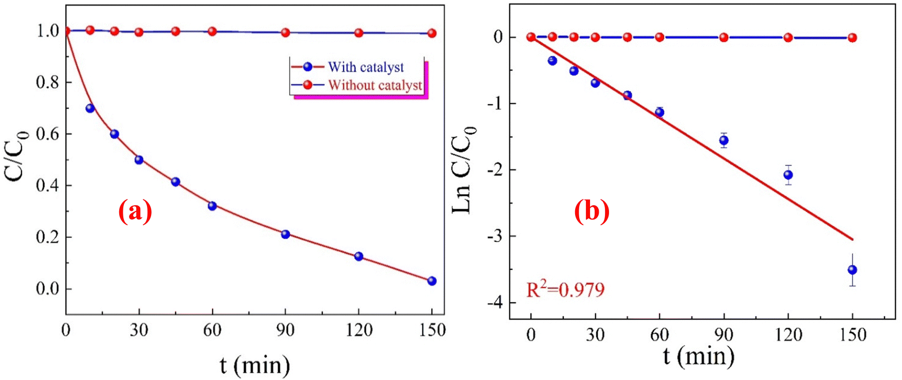 | ||
| Fig. 29 (a) Time-dependent profile of H2O2 degradation with and without catalyst (b) ln(C0/Ct)) versus time. | ||
 | ||
| Fig. 30 Mechanism of decomposition of H2O2 solution in the presence of the CFO nanoparticles as catalyst. | ||
Numerous studies in the literature explore the ability of cobalt ferrite catalysts to decompose hydrogen peroxide. Table S8 (ESI†) compares the catalytic activities of various metal oxides involved in H2O2 decomposition. It is noted that most catalysts demonstrate activity within a range of minimal H2O2 concentrations. For example, H2O2 solutions used in studies7,132 were at low concentrations (<12 mM). However, CFO/C3N4 complex composite catalysts have been employed to break down hydrogen peroxide at slightly higher concentrations (0.01–0.5 M).133 It is possible to enhance the catalytic activity for hydrogen peroxide decomposition by using various irradiation sources.133–135 The primary aim of these studies was to reduce the recombination rate of hydroxyl radicals. The CFO sample in this study has proven to be an exceptionally effective catalyst for H2O2 decomposition. The CFO sample demonstrates the highest first-order rate constant (3.39 × 10⁻⁴ s−1). High-concentration hydrogen peroxide solutions (up to 120 mM) were completely decomposed within three hours. This work highlights the relationship between surface morphology and catalytic behaviour, emphasizing how tuning these features can significantly improve catalytic applications. This high catalytic activity of CFO may be due to its mesoporous structure, high specific surface area (269.67 m2 g−1),21 and small crystallite size (14.78 nm). The high surface area increases the density of active sites, enabling efficient adsorption and interaction of reactants. Combined with mesoporosity, this ensures optimal diffusion and accessibility of hydrogen peroxide molecules during catalytic reactions. The small crystallite size (∼14.78 nm) enhances surface reactivity, promoting electron transfer processes during catalysis. These structural features lead to exceptional catalytic activity.
Unlike our earlier work,21 which primarily focused on the heavy metal, dye removal activity of CFO nanoparticles, structural, magnetic, and optical properties, this study provides a deeper investigation into their dielectric behaviour and interfacial phenomena. Through Havriliak–Negami modelling, we elucidated the role of relaxation dynamics in abnormal semiconducting–insulating–semiconducting transitions, advancing the understanding of how interfacial polarization influences charge carrier mobility. This novel insight establishes the importance of Maxwell–Wagner polarization in designing tunable dielectric materials, a feature not addressed in our previous study. Furthermore, integrating these dielectric properties with enhanced catalytic performance highlights the multifunctionality of CFO nanoparticles, positioning them as superior candidates for advanced applications in optoelectronics and catalysis.
4. Limitations and future directions
Despite these advancements, the study is not without limitations. The long-term stability of CFO nanoparticles under varying environmental conditions needs further investigation to ensure their practical applicability. Additionally, while this work highlights the influence of interfacial phenomena on material performance, the effects of external electric and magnetic fields on dielectric transitions remain unexplored and warrant future research. Finally, optimizing the scalability and consistency of the green synthesis process will be critical for transitioning these materials from laboratory-scale studies to real-world applications. Addressing these challenges will further enhance the versatility and reliability of CFO nanoparticles for advanced technological applications.5. Conclusion
This study significantly advances the surface and interface science field by uncovering the pivotal role of Maxwell–Wagner interfacial polarization in CFO nanoparticles, shedding light on its influence on abnormal semiconductor–insulator–semiconductor transitions. Building on the findings of our earlier work, which primarily focused on the adsorption of heavy metal from wastewater, structural, magnetic, and optical properties, this study delves deeper into the intricate interplay of charge carrier dynamics, structural defects, and relaxation mechanisms, as modelled by the Havriliak–Negami framework. These insights expand the understanding of dielectric behaviour at nanoscale interfaces and establish new paradigms for designing tunable dielectric materials under the influence of temperature.CFO nanoparticles synthesized through a green, sustainable method using Greek yogurt exhibit remarkable structural, optical, and catalytic properties. The direct (1.46 eV) and indirect (0.9 eV) band gaps and observed structural defects significantly impact charge carrier mobility and dielectric behaviour. This study identifies Maxwell–Wagner interfacial polarization as the dominant mechanism in these nanoparticles, arising from charge carrier interactions at the interfaces between conducting grains and insulating grain boundaries. These interfacial dynamics drive the observed semiconductor–insulator–semiconductor transitions, further influenced by polaron hopping, defect states, and temperature-dependent relaxation dynamics. The resulting insights into polarization mechanisms at nano-interfaces represent a substantial advancement in surface and interface science.
Moreover, the exceptional catalytic performance of CFO nanoparticles, achieving 97% hydrogen peroxide degradation in just 150 minutes (rate constant: 3.39 × 10⁻⁴ s−1), underscores their multifunctionality. The high specific surface area (269.67 m2 g−1) and small crystallite size (14.78 nm) enhance catalytic efficiency by providing abundant active sites and efficient diffusion pathways for reactants and products. This synergy between structural properties and functional performance positions CFO nanoparticles as superior candidates for various applications, including optoelectronics, catalysis, and energy storage.
By bridging eco-friendly synthesis methods with advanced interface engineering, this study establishes a critical link between nanoscale structural attributes, such as surface area and porosity, and functional outcomes. It not only deepens the understanding of interfacial dynamics but also showcases the transformative potential of leveraging these phenomena to optimize material performance. The findings set a benchmark for integrating sustainability with cutting-edge functional materials, paving the way for innovative solutions in advanced material science. This work highlights the immense potential of CFO nanoparticles to drive next-generation technologies, laying the foundation for future research to enhance their stability and scalability for broader real-world applications.
Author contributions
This work was conceptualized by Heba Hussein, S. S. Ibrahim, and Sherif A. Khairy. Heba Hussein conducted the experiments, wrote the main text, and prepared the figures. All contributors reviewed the manuscript, and all authors approved the final version.Data availability
Upon a reasonable request, the corresponding author will provide the data supporting the study's conclusions.Conflicts of interest
There is no conflict to declare.References
- S. Banifatemi, et al., Green synthesis of CoFe2O4 nanoparticles using olive leaf extract and characterization of their magnetic properties, Ceram. Int., 2021, 47(13), 19198–19204 Search PubMed.
- A. Manohar, et al., Synthesis, characterization and magnetic hyperthermia properties of nearly monodisperse CoFe2O4 nanoparticles, Ceram. Int., 2020, 46(18), 28035–28041 CrossRef CAS.
- N. Dhanda, P. Thakur and A. Thakur, Green synthesis of cobalt ferrite: a study of structural and optical properties, Mater. Today: Proc., 2023, 73, 237–240 CAS.
- A. Kiani, F. Davar and M. Bazarganipour, Influence of verjuice extract on the morphology, phase, and magnetic properties of green synthesized CoFe2O4 nanoparticle: its application as an anticancer drug delivery, Ceram. Int., 2022, 48(23), 34895–34906 CrossRef CAS.
- Z. Cao and C. Zuo, Direct synthesis of magnetic CoFe2O4 nanoparticles as recyclable photo-Fenton catalysts for removing organic dyes, ACS Omega, 2020, 5(35), 22614–22620 CrossRef CAS PubMed.
- A. Hassani, et al., Heterogeneous sono-Fenton-like process using magnetic cobalt ferrite-reduced graphene oxide (CoFe2O4–rGO) nanocomposite for the removal of organic dyes from aqueous solution, Ultrason. Sonochem., 2018, 40, 841–852 CrossRef CAS PubMed.
- K. Pan, et al., Oxygen vacancy mediated surface charge redistribution of Cu-substituted LaFeO3 for degradation of bisphenol A by efficient decomposition of H2O2, J. Hazard. Mater., 2020, 389, 122072 CrossRef CAS PubMed.
- J. Weiss, The free radical mechanism in the reactions of hydrogen peroxide, Adv. Catal., 1952, 343–365 CAS , Elsevier.
- Z. Liu, et al., Kinetic and mechanistic study on catalytic decomposition of hydrogen peroxide on carbon-nanodots/graphitic carbon nitride composite, Catalysts, 2018, 8(10), 445 CrossRef.
- T. Tatarchuk, et al., Spinel cobalt(II) ferrite-chromites as catalysts for H2O2 decomposition: Synthesis, morphology, cation distribution and antistructure model of active centers formation, Ceram. Int., 2020, 46(17), 27517–27530 CrossRef CAS.
- R. Curci and J. O. Edwards, Activation of hydrogen peroxide by organic compounds, in Catalytic oxidations with hydrogen peroxide as oxidant, Springer, 1992, pp. 45–95 Search PubMed.
- L. Ershadi Afshar, N. Chaibakhsh and Z. Moradi-Shoeili, Treatment of wastewater containing cytotoxic drugs by CoFe2O4 nanoparticles in Fenton/ozone oxidation process, Sep. Sci. Technol., 2018, 53(16), 2671–2682 CrossRef CAS.
- H. Nikmanesh and M. Eshraghi, Cation distribution, magnetic and structural properties of CoCrxFe2−xO4: effect of calcination temperature and chromium substitution, J. Magn. Magn. Mater., 2019, 471, 294–303 CrossRef CAS.
- B. Dash, et al., Investigation of Substitution of Nickel Cations in Cobalt Ferrite (CoFe2O4) Nanoparticles and Their Influence on Frequency and Temperature Dependent Dielectric and Magnetodielectric Properties, Trans. Electr. Electron. Mater., 2024, 1–15 Search PubMed.
- K. Dhabekar and K. M. Kant, Structural and dielectric properties of cobalt ferrite based nanocomposites, Phys. B, 2021, 603, 412752 CrossRef CAS.
- M. George, et al., Finite size effects on the electrical properties of sol–gel synthesized CoFe2O4 powders: deviation from Maxwell–Wagner theory and evidence of surface polarization effects, J. Phys. D: Appl. Phys., 2007, 40(6), 1593 CrossRef CAS.
- K. L. Routray, S. Saha and D. Behera, Insight into the anomalous electrical behavior, dielectric and magnetic study of Ag-Doped CoFe2O4 synthesised by Okra extract-assisted green synthesis, J. Electron. Mater., 2020, 49, 7244–7258 CrossRef.
- A. Shanmugavani, et al., Influence of pH and fuels on the combustion synthesis, structural, morphological, electrical and magnetic properties of CoFe2O4 nanoparticles, Mater. Res. Bull., 2015, 71, 122–132 CrossRef CAS.
- R. Panda and D. Behera, Investigation of electric transport behavior of bulk CoFe2O4 by complex impedance spectroscopy, J. Alloys Compd., 2014, 587, 481–486 CrossRef CAS.
- V. K. Sharma, R. Nathawat and S. S. Rathore, Structural, thermal and dielectric studies of mixed spinel CoFe2O4, Mater. Today: Proc., 2021, 46, 2193–2196 CAS.
- H. Hussein, S. Ibrahim and S. A. Khairy, Biosynthesis of CoFe2O4 ferrite nanoparticles using Greek yogurt solution: Deep structural insights and appraisal for ecological mitigation via quartz crystal microbalance, J. Water Process Eng., 2024, 65, 105856 CrossRef.
- Y. M. Abbas, et al., Investigation of structural and magnetic properties of multiferroic La1−xYxFeO3 Perovskites, prepared by citrate auto-combustion technique, J. Magn. Magn. Mater., 2019, 482, 66–74 CrossRef CAS.
- M. Bhagwat, et al., Rietveld refinement study of nanocrystalline copper doped zirconia, Mater. Res. Bull., 2003, 38(13), 1713–1724 CrossRef CAS.
- V. Fuster, et al., Characterization of phases in an Fe–Mn–Si–Cr–Ni shape memory alloy processed by different thermomechanical methods, Mater. Charact., 2015, 109, 128–137 CrossRef CAS.
- B. D. Cullity, Elements of X-ray Diffraction, Addison-Wesley Publishing, 1956 Search PubMed.
- P. Monisha, et al., Influence of Mn dopant on the crystallite size, optical and magnetic behaviour of CoFe2O4 magnetic nanoparticles, J. Phys. Chem. Solids, 2021, 148, 109654 CrossRef CAS.
- L. Weil, F. Bertaut and L. Bochirol, Propriétés magnétiques et structure de la phase quadratique du ferrite de cuivre, J. Phys. Radium, 1950, 11(5), 208–212 CrossRef CAS.
- T. Tatarchuk, et al., Structure–redox reactivity relationships in Co1−xZnxFe2O4: the role of stoichiometry, New J. Chem., 2019, 43(7), 3038–3049 RSC.
- S. Debnath, et al., X-ray diffraction analysis for the determination of elastic properties of zinc-doped manganese spinel ferrite nanocrystals (Mn0.75Zn0.25Fe2O4), along with the determination of ionic radii, bond lengths, and hopping lengths, J. Phys. Chem. Solids, 2019, 134, 105–114 CrossRef CAS.
- K. Khalaf, et al., Influence of Zn2+ ions on the structural and electrical properties of Mg1−xZnxFeCrO4 spinels, J. Alloys Compd., 2016, 657, 733–747 CrossRef CAS.
- K. Mohamedda, et al., Infrared and structural studies of Mg–Zn ferrite, Physica B, 2012, 407, 795–804 CrossRef.
- T. K. C. Nguyen and A. T. Nguyen, Structural, optical and magnetic properties of Y-doped CoFe2O4 nanoparticles prepared by a simple co-precipitation method, J. Mater. Sci.: Mater. Electron., 2023, 34(5), 448 CrossRef CAS.
- R. Rai, et al., Optical and electronic properties of NiFe2O4 and CoFe2O4 thin films, Appl. Phys. A: Mater. Sci. Process., 2012, 106, 207–211 CrossRef CAS.
- B. Zhou, et al., Correlation between structure and intervalence charge-transfer transitions in nanocrystalline CoFe2−xMxO4 (M = Mn, Al, Sc) thin films, Phys. Rev. B: Condens. Matter Mater. Phys., 2003, 68(2), 024426 CrossRef.
- R. G. Burns, Mineralogical applications of crystal field theory, Cambridge University Press, 1993 Search PubMed.
- M. N. Taran and G. R. Rossman, Optical spectra of Co2+ in three synthetic silicate minerals, Am. Mineral., 2001, 86(7–8), 889–895 CrossRef CAS.
- J. A. Barreda-Argüeso, et al., Pressure-induced spin transition and site-selective metallization in CoCl2, Sci. Rep., 2019, 9(1), 5448 CrossRef PubMed.
- O. Rejaiba, et al., Investigation study of optical and dielectric parameters using absorption and diffuse reflectance spectroscopy method on La0.57Nd0.1Sr0.13Ag0.2MnO3 perovskite for optoelectronic application, Opt. Quantum Electron., 2022, 54(5), 315 CrossRef CAS.
- W. E. Vargas and G. A. Niklasson, Applicability conditions of the Kubelka–Munk theory, Appl. Opt., 1997, 36(22), 5580–5586 CrossRef CAS PubMed.
- L. Yang and B. Kruse, Revised Kubelka–Munk theory. I. Theory and application, J. Opt. Soc. Am. A, 2004, 21(10), 1933–1941 CrossRef PubMed.
- B. Lakshmi, B. J. Thomas and P. Gopinath, Accurate band gap determination of chemically synthesized cobalt ferrite nanoparticles using diffuse reflectance spectroscopy, Adv. Powder Technol., 2021, 32(10), 3706–3716 CrossRef CAS.
- W. Fontijn, et al., A consistent interpretation of the magneto-optical spectra of spinel type ferrites, J. Appl. Phys., 1999, 85(8), 5100–5105 CrossRef CAS.
- I. Gul, et al., Optical, magnetic and electrical investigation of cobalt ferrite nanoparticles synthesized by co-precipitation route, J. Alloys Compd., 2010, 507(1), 201–206 CrossRef CAS.
- C. Himcinschi, et al., Optical and magneto-optical study of nickel and cobalt ferrite epitaxial thin films and submicron structures, J. Appl. Phys., 2013, 113, 084101 CrossRef.
- B. Holinsworth, et al., Chemical tuning of the optical band gap in spinel ferrites: CoFe2O4vs. NiFe2O4, Appl. Phys. Lett., 2013, 103(8), 082406 CrossRef.
- C. Kittel, Introduction to solid state physics, 8th edn, 2021 Search PubMed.
- V. Akshay, et al., Visible range optical absorption, Urbach energy estimation and paramagnetic response in Cr-doped TiO2 nanocrystals derived by a sol–gel method, Phys. Chem. Chem. Phys., 2019, 21(24), 12991–13004 RSC.
- S. K. Paswan, et al., Optimization of structure-property relationships in nickel ferrite nanoparticles annealed at different temperature, J. Phys. Chem. Solids, 2021, 151, 109928 CrossRef CAS.
- H. Dhibi, et al., Comprehensive investigation of structural, morphologic, optical, dielectric and electrical of Ni0.3Cd0.7Cr2O4 chromite to optoelectronic application, J. Inorg. Organomet. Polym. Mater., 2023, 33(12), 3984–4000 CrossRef CAS.
- A. B. J. Kharrat, K. Kahouli and S. Chaabouni, Detailed investigation of the optical properties of the (C8H11BrN)3BiCl6 compound by UV-visible measurements, Bull. Mater. Sci., 2020, 43(1), 275 CrossRef CAS.
- F. Hcini, et al., Thermal, microstructural, optical, magnetic and magnetocaloric studies for Ni0.5Mn0.5Cr2O4 chromite spinel prepared using sol–gel method, J. Mol. Struct., 2021, 1243, 130769 CrossRef CAS.
- F. Hcini, et al., Structural, optical, and dielectric properties for Mg0.6Cu0.2Ni0.2Cr2O4 chromite spinel, Phys. B, 2022, 624, 413439 CrossRef CAS.
- M. Okutan, et al., Investigation of refractive index dispersion and electrical properties in carbon nano-balls’ doped nematic liquid crystals, Phys. B, 2005, 362(1–4), 180–186 CrossRef CAS.
- M. Fox, Optical properties of solids, Oxford University Press, 2010, vol. 3 Search PubMed.
- N. Mahfoudh, K. Karoui and A. BenRhaiem, Optical studies and dielectric response of [DMA]2MCl4 (M = Zn and Co) and [DMA]2ZnBr4, RSC Adv., 2021, 11(40), 24526–24535 RSC.
- Z. Raddaoui, et al., Correlation of crystal structure and optical properties of Ba0.97Nd0.0267Ti(1−x)WxO3 perovskite, RSC Adv., 2018, 8(49), 27870–27880 RSC.
- R. Kannan, et al., Unusual metallic behavior in nanostructured cobalt ferrite at superparamagnetic regime, J. Appl. Phys., 2012, 112(6), 063926 CrossRef.
- J. B. Goodenough, Direct cation–cation interactions in several oxides, Phys. Rev., 1960, 117(6), 1442–1451 CrossRef CAS.
- J. Venturini, et al., Conductivity dynamics of metallic-to-insulator transition near room temperature in normal spinel CoFe2O4 nanoparticles, J. Mater. Chem. C, 2018, 6(17), 4720–4726 RSC.
- D. Bouokkeze, et al., Investigation of the structural, optical, elastic and electrical properties of spinel LiZn2Fe3O8 nanoparticles annealed at two distinct temperatures, RSC Adv., 2019, 9, 40940–40955 RSC.
- S. Mandal, et al., Frequency and temperature dependence of dielectric and electrical properties of TFe2O4 (T = Ni, Zn, Zn0.5Ni0.5) ferrite nanocrystals, J. Alloys Compd., 2016, 656, 887–896 CrossRef CAS.
- K. Abdouli, et al., Investigation of the structural, electrical, and dielectric properties of La0.5Sm0.2Sr0.3Mn1−xCrxO3 for electrical application, RSC Adv., 2022, 12(26), 16805–16822 RSC.
- K. Funke, Jump relaxation in solid electrolytes, Prog. Solid State Chem., 1993, 22(2), 111–195 CrossRef CAS.
- S. Karthickprabhu, et al., Structural and electrical studies on Zn2+ doped LiCoPO4, J. Electrost., 2014, 72(3), 181–186 CrossRef CAS.
- Y. Ben Taher, et al., Conductivity study and correlated barrier hopping (CBH) conduction mechanism in diphosphate compound, Appl. Phys. A: Mater. Sci. Process., 2015, 120, 1537–1543 CrossRef CAS.
- D. Bouokkeze, et al., Investigation of the structural, optical, elastic and electrical properties of spinel LiZn2Fe3O8 nanoparticles annealed at two distinct temperatures, RSC Adv., 2019, 9(70), 40940–40955 RSC.
- S. Bhukal, et al., Influence of Cd2+ ions on the structural, electrical, optical and magnetic properties of Co–Zn nanoferrites prepared by sol gel auto combustion method, J. Mol. Struct., 2014, 1071, 95–102 CrossRef CAS.
- S. Bhukal, et al., Structural, electrical, optical and magnetic properties of chromium substituted Co–Zn nanoferrites Co0.6Zn0.4CrxFe2−xO4 (0 ≤ x ≤ 1.0) prepared via sol–gel auto-combustion method, J. Mol. Struct., 2012, 1012, 162–167 CrossRef CAS.
- M. Idrees, et al., Origin of colossal dielectric response in LaFeO3, Acta Mater., 2011, 59(4), 1338–1345 CrossRef CAS.
- S. Amor, et al., Modulation of magnetism and study of impedance and alternating current conductivity of Zn0.4Ni0.6Fe2O4 spinel ferrite, J. Mol. Struct., 2019, 1184, 298–304 CrossRef CAS.
- D. Venkatesh and K. Ramesh, Structural, dielectric and impedance spectroscopic studies of Ni0.5Zn0.5−xLixFe2O4 nanocrystalline ferrites, Int. J. Mod. Phys. B, 2017, 31(22), 1750153 CrossRef CAS.
- G. Pike, AC conductivity of scandium oxide and a new hopping model for conductivity, Phys. Rev. B, 1972, 6(4), 1572 CrossRef CAS.
- S. Elliott, A theory of ac conduction in chalcogenide glasses, Philos. Mag., 1977, 36(6), 1291–1304 CrossRef CAS.
- P. Bruce, High and low frequency Jonscher behaviour of an ionically conducting glass, Solid State Ionics, 1985, 15(3), 247–251 CrossRef CAS.
- Y. Moualhi, et al., Double Jonscher response and contribution of multiple mechanisms in electrical conductivity processes of Fe-PrCaMnO ceramic, Ceram. Int., 2020, 46(2), 1601–1608 CrossRef CAS.
- Y. Moualhi, et al., Superlinear dependence of the conductivity, double/single Jonscher variations and the contribution of various conduction mechanisms in transport properties of La0.5Ca0.2Ag0.3MnO3 manganite, J. Alloys Compd., 2022, 898, 162866 CrossRef CAS.
- N. Ponpandian, P. Balaya and A. Narayanasamy, Electrical conductivity and dielectric behaviour of nanocrystalline NiFe2O4 spinel, J. Phys.: Condens. Matter, 2002, 14(12), 3221 CrossRef CAS.
- M. H. Dhaou, et al., Structural and complex impedance spectroscopic studies of Ni0.5Mg0.3Cu0.2Fe2O4 ferrite nanoparticle, Appl. Phys. A: Mater. Sci. Process., 2017, 123, 1–9 CrossRef CAS.
- A. K. Jonscher, The ‘universal’dielectric response, Nature, 1977, 267(5613), 673–679 CrossRef CAS.
- A. Avogadro, et al., B11 spin-lattice relaxation and disorder modes in ionic glassy conductors (AgI)x(Ag2O·nB2O3)1−x, Phys. Rev. B: Condens. Matter Mater. Phys., 1990, 41(10), 6137 CrossRef CAS PubMed.
- N. Baskaran, G. Govindaraj and A. Narayanasamy, Ac conductivity and relaxation processes in silver selenochromate glass, Solid State Ionics, 1997, 98(3–4), 217–227 CrossRef CAS.
- C. Cramer and M. Buscher, Complete conductivity spectra of fast ion conducting silver iodide/silver selenate glasses, Solid State Ionics, 1998, 105(1–4), 109–120 CrossRef CAS.
- M. Cutroni and A. Mandanici, Mechanical and dielectric behaviour of some ionic glasses, Solid State Ionics, 1998, 105(1–4), 149–157 CrossRef CAS.
- M. Cutroni, et al., Conductivity dynamical response in (AgI)x(AgPO3)1−x glasses, Solid State Ionics, 2002, 154, 713–717 CrossRef.
- J. Dieckhöfer, et al., Composition dependence of low-frequency excitations in lithium silicophosphate glasses by nuclear magnetic resonance and electrical conductivity, Phys. Rev. B: Condens. Matter Mater. Phys., 1997, 55(22), 14836 CrossRef.
- M. Le Stanguennec and S. Elliott, Frequency-dependent ionic conductivity in AgI–AgPO3 glasses, Solid State Ionics, 1994, 73(3–4), 199–208 CrossRef CAS.
- P. Lunkenheimer and A. Loidl, Response of disordered matter to electromagnetic fields, Phys. Rev. Lett., 2003, 91(20), 207601 CrossRef CAS PubMed.
- B. Roling, et al., Role of AgI for ionic conduction in AgI–AgPO3 glasses, Phys. Rev. B: Condens. Matter Mater. Phys., 1997, 56(21), 13619 CrossRef CAS.
- D. Singh, K. Shahi and K. K. Kar, Superlinear frequency dependence of AC conductivity and its scaling behavior in xAgI-(1 − x) AgPO3 glass superionic conductors, Solid State Ionics, 2016, 287, 89–96 CrossRef CAS.
- D. P. Singh, K. Shahi and K. K. Kar, Scaling behavior and nearly constant loss effect in AgI–LiPO3 composite glasses, Solid State Ionics, 2013, 231, 102–108 CrossRef CAS.
- J. Tiwari and K. Shahi, Super-linear frequency dependence of ac conductivity of disordered Ag2S–Sb2S3 at cryogenic temperatures, Philos. Mag., 2007, 87(29), 4475–4500 CrossRef CAS.
- S. Elliott, On the super-linear frequency dependent conductivity of amorphous semiconductors, Solid State Commun., 1978, 28(11), 939–942 CrossRef CAS.
- A. Long and N. Balkan, AC loss in amorphous germanium, Philos. Mag. B, 1980, 41(3), 287–305 CAS.
- A. Ghosh, Frequency-dependent conductivity in bismuth-vanadate glassy semiconductors, Phys. Rev. B: Condens. Matter Mater. Phys., 1990, 41(3), 1479 CrossRef CAS PubMed.
- M. H. Dhaou, A. Mallah and A. Alsawi, Dielectric Relaxation and Non-Overlapping Small Polaron Tunneling Model Conduction Studies of Ag2−xNaxZnP2O7 (x = 0, 1, and 2) Materials, Cryst. Res. Technol., 2021, 56(9), 2100035 CrossRef CAS.
- M. B. Bechir and M. H. Dhaou, Study of charge transfer mechanism and dielectric relaxation of all-inorganic perovskite CsSnCl3, RSC Adv., 2021, 11(35), 21767–21780 RSC.
- S. S. Jadhav, et al., Structural and electric properties of zinc substituted NiFe2O4 nanoparticles prepared by co-precipitation method, Phys. B, 2010, 405(12), 2610–2614 CrossRef CAS.
- S. Kumar, et al., Structural, magnetic, and electrical properties of CoFe2O4 nanostructures synthesized using microwave-assisted hydrothermal method, Materials, 2022, 15(22), 7955 CrossRef CAS PubMed.
- G. Jonker, Magnetic compounds with perovskite structure IV Conducting and non-conducting compounds, Physica, 1956, 22(6–12), 707–722 CrossRef CAS.
- B. Kaur, et al., AC impedance spectroscopy, conductivity and optical studies of Sr doped bismuth ferrite nanocomposites, Int. J. Electrochem. Sci., 2016, 11(5), 4120–4135 CrossRef CAS.
- M. Arora, et al., Evidence of spin-two phonon coupling and improved multiferroic behavior of Bi1−xDyxFeO3 nanoparticles, Ceram. Int., 2014, 40(8), 13347–13356 CrossRef CAS.
- P. Pandit, S. Satapathy and P. Gupta, Effect of La substitution on conductivity and dielectric properties of Bi1−xLaxFeO3 ceramics: An impedance spectroscopy analysis, Phys. B, 2011, 406(13), 2669–2677 CrossRef CAS.
- C. Behera, P. R. Das and R. Choudhary, Structural and electrical properties of mechanothermally synthesized NiFe2O4 nanoceramics, J. Electron. Mater., 2014, 43, 3539–3549 CrossRef CAS.
- A. R. Chavan, et al., Cu2+ substituted NiFe2O4 thin films via spray pyrolysis technique and their high-frequency devices application, J. Alloys Compd., 2018, 769, 1132–1145 CrossRef CAS.
- F. Hcini, et al., Effects of sintering temperature on structural, infrared, magnetic and electrical properties of Cd0.5Zn0.5FeCrO4 ferrites prepared by sol–gel route, J. Mater. Sci.: Mater. Electron., 2020, 31, 14986–14997 CrossRef CAS.
- C. Koops, On the dispersion of resistivity and dielectric constant of some semiconductors at audiofrequencies, Phys. Rev., 1951, 83(1), 121 CrossRef CAS.
- J. C. Maxwell, A treatise on electricity and magnetism, Clarendon Press google schola, 1873, vol. 2, pp. 3408–3425 Search PubMed.
- K. Hussain, N. Amin and M. I. Arshad, Evaluation of structural, optical, dielectric, electrical, and magnetic properties of Ce3+ doped Cu0.5Cd0.25Co0.25Fe2−xO4 spinel nano-ferrites, Ceram. Int., 2021, 47(3), 3401–3410 CrossRef CAS.
- M. Junaid, et al., Structural, microstructural, spectral, and dielectric properties of erbium substituted spinel ferrites, Phys. B, 2022, 641, 414120 CrossRef CAS.
- S. Hcini, et al., Studies of structural, dielectric, and optical properties of CuCoFeO4 spinel for high frequency, microwave, and optoelectronic applications, J. Mol. Struct., 2023, 1291, 135981 CrossRef CAS.
- V. Khopkar and B. Sahoo, Low temperature dielectric properties and NTCR behavior of the BaFe0.5Nb0.5O3 double perovskite ceramic, Phys. Chem. Chem. Phys., 2020, 22(5), 2986–2998 RSC.
- S. Sen, R. Parida and B. Parida, Havriliak–Negami and Bergman type of dielectric response, together with Dyre's Hopping tunneling through random free energy barriers in (BiFeO3)0.8—(CaTiO3)0.2 distorted crystalline structure, J. Mater. Sci.: Mater. Electron., 2023, 34(22), 1617 CrossRef CAS.
- J. C. Maxwell, Electricity and magnetism, Dover New York, 1954, vol. 2 Search PubMed.
- K. W. Wagner, Zur theorie der unvollkommenen dielektrika, Ann. Phys., 1913, 345(5), 817–855 CrossRef.
- J. Joshi, et al., Complex impedance, FT-Raman, and photoluminescence spectroscopic studies of pure and L-phenylalanine doped ammonium dihydrogen phosphate single crystals: the correlation with hydrogen bonding defect, Ionics, 2019, 25, 3223–3245 CrossRef CAS.
- J. Giuntini, et al., Temperature dependence of dielectric losses in chalcogenide glasses, J. Non-Cryst. Solids, 1981, 45(1), 57–62 CrossRef CAS.
- O. Madelung et al. , Electrical Conductivity II/Elektrische Leitungsphänomene II, Springer-Verlag, vol. 4, 2013 Search PubMed.
- H. Zaki, AC conductivity and frequency dependence of the dielectric properties for copper doped magnetite, Phys. B, 2005, 363(1–4), 232–244 CrossRef CAS.
- K. Iwauchi, Magnetic and Dielectric Relaxations in Ferrites, Bull. Inst. Chem. Res., Kyoto Univ., 1983, 61(4), 324–333 CAS.
- N. Rezlescu and E. Rezlescu, Abnormal dielectric behaviour of copper containing ferrites, Solid State Commun., 1974, 14(1), 69–72 CrossRef CAS.
- M. Idrees, M. Nadeem and M. Hassan, Investigation of conduction and relaxation phenomena in LaFe0.9Ni0.1O3 by impedance spectroscopy, J. Phys. D: Appl. Phys., 2010, 43(15), 155401 CrossRef.
- M. B. Reddy and P. V. Reddy, Low-frequency dielectric behaviour of mixed Li–Ti ferrites, J. Phys. D: Appl. Phys., 1991, 24(6), 975 CrossRef CAS.
- T. Dabbebi, et al., Structural and dielectric behaviors for Mg0.5Co0.5Fe2O4 spinel ferrite synthesized by sol–gel route, J. Mater. Sci.: Mater. Electron., 2022, 1–15 Search PubMed.
- M. B. Hossen and A. A. Hossain, Frequency and temperature dependent transport properties of NiCuZn ceramic oxide, Mater. Sci.-Pol., 2015, 33(2), 259–267 CrossRef CAS.
- E. Ateia, M. Ahmed and R. Ghouniem, Effect of rare earth substitution on the structural and electrical properties of Cu–Mg ferrite, Int. J. Mod. Phys. B, 2015, 29(19), 1550126 CrossRef CAS.
- H. Eyring, Viscosity, plasticity, J. Chem. Phys., 1936, 4, 291 Search PubMed.
- A. V. Sarode and A. C. Kumbharkhane, Dielectric relaxation study of poly (ethylene glycols) using TDR technique, J. Mol. Liq., 2011, 164(3), 226–232 CrossRef CAS.
- G. Lal, et al., Exploring the structural, elastic, optical, dielectric and magnetic characteristics of Ca2+ incorporated superparamagnetic Zn0.5−xCa0.1Co0.4+xFe2O4 (x = 0.0, 0.05 & 0.1) nanoferrites, J. Alloys Compd., 2021, 886, 161190 CrossRef CAS.
- J. H. Lee, et al., High performance H2O2 production achieved by sulfur-doped carbon on CdS photocatalyst via inhibiting reverse H2O2 decomposition, Appl. Catal., B, 2021, 284, 119690 CrossRef CAS.
- H. Luo, et al., Enhanced decomposition of H2O2 by molybdenum disulfide in a Fenton-like process for abatement of organic micropollutants, Sci. Total Environ., 2020, 732, 139335 CrossRef CAS PubMed.
- N. T. To Loan, et al., CoFe2O4 nanomaterials: effect of annealing temperature on characterization, magnetic, photocatalytic, and photo-Fenton properties, Processes, 2019, 7(12), 885 CrossRef.
- X. Guo, H. Li and S. Zhao, Fast degradation of Acid Orange II by bicarbonate-activated hydrogen peroxide with a magnetic S-modified CoFe2O4 catalyst, J. Taiwan Inst. Chem. Eng., 2015, 55, 90–100 CrossRef CAS.
- Y. Yao, et al., Enhanced photo-Fenton-like process over Z-scheme CoFe2O4/gC3N4 heterostructures under natural indoor light, Environ. Sci. Pollut. Res., 2016, 23, 21833–21845 CrossRef CAS PubMed.
- Y. Deng, et al., Magnetic recyclable CoFe2O4@PPy prepared by in situ Fenton oxidization polymerization with advanced photo-Fenton performance, RSC Adv., 2020, 10(4), 1858–1869 RSC.
- H.-Y. He and J. Lu, Highly photocatalytic activities of magnetically separable reduced graphene oxide-CoFe2O4 hybrid nanostructures in dye photodegradation, Sep. Purif. Technol., 2017, 100(172), 374–381 CrossRef.
Footnote |
| † Electronic supplementary information (ESI) available. See DOI: https://doi.org/10.1039/d4ma01172d |
| This journal is © The Royal Society of Chemistry 2025 |