
 Open Access Article
 This Open Access Article is licensed under a Creative Commons Attribution-Non Commercial 3.0 Unported Licence
Origin and enhancement of the piezoelectricity in monolayer group IV monochalcogenides under strain and in the presence of vacancies
Arun
Jangir
a,
Duc Tam
Ho
 b and
Udo
Schwingenschlögl
*a
b and
Udo
Schwingenschlögl
*a
aPhysical Science and Engineering Division, King Abdullah University of Science and Technology (KAUST), Thuwal 23955-6900, Saudi Arabia. E-mail: udo.schwingenschlogl@kaust.edu.sa
bDepartment of Mechanical and Construction Engineering, Northumbria University, Newcastle Upon Tyne NE1 8ST, UK
First published on 28th November 2024
Abstract
Piezoelectric materials are a critical component in many electronic devices from the nanoscale to the macroscale. Monolayer group IV monochalcogenides can provide particularly large piezoelectric coefficients. To investigate the origin of this strong piezoelectricity, we conduct an atomic-level analysis of the charge redistribution under mechanical strain. Our results show that it arises from charge transfer between strong and weak chemical bonds. We demonstrate that the piezoelectric coefficients can be substantially enhanced by mechanical strain and the presence of vacancies, for instance in the case of monolayer SnSe by up to 112% by 2% compression and by up to 433% by an Sn–Se vacancy density of 5.5%.
1. Introduction
Electro-mechanical coupling (piezoelectricity), which exists only in non-centrosymmetric materials, is the generation of deformation by an electric field, and vice versa. Piezoelectric materials have a wide range of applications from the nanoscale to the macroscale, such as accelerometers,1 sensors,2 resonators,3 bioprobes,4 nanogenerators,5,6 actuators,7 scaffolds,8 and bone-growth stimulators.9 While three-dimensional piezoelectric materials (organic, inorganic, composite, bio-inspired, etc.) and their nanostructures (nanotubes, nanowires, nanorings, etc.) are well known, the research on two-dimensional piezoelectric materials accelerates only since monolayer MoS2 was shown to perform comparably to three-dimensional ZnO.10–12 The possibility to tailor the properties of two-dimensional piezoelectric materials by methods such as stacking, functionalization, and defect engineering opens excellent prospects for their integration in future electro-mechanical systems.Some monolayer materials exhibit intrinsic piezoelectricity, such as transition metal dichalcogenides,13 group II oxides,13 hexagonal III–V semiconductors,13 group III monochalcogenides,14 group IV monochalcogenides,15–17 and α-In2Se3.18 In addition, piezoelectric response can be induced extrinsically in graphene by ad-atom adsorption,19 triangular cutting,20 and bending.21 The piezoelectric coefficients of the monolayer group IV monochalcogenides are several orders of magnitude higher than those of other two-dimensional materials due to their puckered structure,15 which also allows the materials to sustain large strain without failure.22 The atomistic mechanism leading to the high piezoelectric coefficients, however, is largely unknown. The same applies to the effect of vacancies, which hold great promise to enhance the piezoelectricity, as their concentration can be well controlled by lithiation.23 For these reasons, we investigate in the present study the piezoelectric coefficients of the monolayer group IV monochalcogenides GeS, GeSe, SnS, and SnSe by first-principles calculations. Using geometrical, crystal orbital Hamilton population, and valence charge density analyses, we show that distinct charge transfer between strong and weak chemical bonds is the origin of the strong piezoelectricity and that this charge transfer can be enhanced by mechanical strain and the presence of vacancies.
2. Computational details
We perform first-principles calculations using the Vienna ab initio simulation package24 (projector augmented wave method with 600 eV plane wave energy cutoff). The Perdew–Burke–Ernzerhof exchange correlation functional is adopted together with an energy convergence criterion of 10−7 eV, 16 × 16 × 1 Monkhorst–Pack k-grids for unit cells, and Monkhorst–Pack k-grids of the same density for supercells. All structures are relaxed using the variable cell method until no atomic force component exceeds 10−3 eV Å−1. The polarization Pi(εjk), where εjk represents the strain and i, j, k = 1, 2, and 3 represents the x, y, and z-axis, respectively, is obtained by the Berry phase approach.25,26 After second degree polynomial fitting of Pi(εjk), the components of the piezoelectric tensor e are computed as27 | (1) |
| eijk = dilmClmjk, | (2) |
resulting in
 | (3) |
 | (4) |
3. Results and discussion
Fig. 1(a) shows the atomic arrangement of the monolayer group IV monochalcogenides, which consist of two atomic layers forming a puckered structure. The armchair and zigzag directions are parallel to the x- and y-axes, respectively. The two atomic layers are connected by vertical bonds (lv), whereas there are strong (ls; short) and weak (lw; long) intralayer bonds. Polarization is present along the x-axis, but not along the y-axis because of the mirror plane perpendicular to this axis. To study the effect of vacancies, a pair of Sn and Se atoms (Sn–Se vacancy) or a single Se atom is removed from 3 × 3, 4 × 4, and 5 × 5 supercells of SnSe (SnSe-p3, SnSe-p4, SnSe-p5, SnSe-s3, SnSe-s4, and SnSe-s5, respectively). The unrelaxed structures of SnSe-p4 and SnSe-s4 are shown in Fig. 1(b) and (c). Sn–Se and Se vacancies are observed experimentally23 and first-principles calculations show that they maintain the semiconducting state.28 | ||
| Fig. 1 (a) Crystal structure of the monolayer group IV monochalcogenides GeS, GeSe, SnS, and SnSe, where lv, ls, and lw represent the bond lengths of the vertical, strong, and weak bonds, respectively. Top view of a 4 × 4 supercell of SnSe with (b) a pair of Sn and Se atoms removed (SnSe-p4) and (c) a single Se atom removed (SnSe-s4). | ||
The relaxed lattice parameters, bond lengths, elastic constants, and piezoelectric coefficients of the investigated monolayers are summarized in Table 1. The results agree well with the e111 values of ref. 15 (5 × 10⁻¹⁰ C m−1 for GeS, 12 × 10−10 C m−1 for GeSe, 18 × 10−10 C m−1 for SnS, and 35 × 10−10 C m−1 for SnSe) but not with the e122 values of ref. 15 (−10 × 10−10 C m−1 for GeS, −8 × 10⁻¹⁰ C m−1 for GeSe, −14 × 10−10 C m−1 for SnS, and 11 × 10−10 C m−1 for SnSe), which is due to the fact that the second and third terms of eqn (1) are omitted in ref. 15. Both e111 and d111 are comparable to the literature values for F-AlN-H (e111 = 9 × 10⁻¹⁰ C m−1, d111 = 16 pm V−1),29 CrTe2 (e111 = 7 × 10⁻¹⁰ C m−1, d111 = 13 pm V−1),14 TmS (e111 = 6 × 10⁻¹⁰ C m−1, d111 = 61 pm V−1),30 Te2Se (e111 = 5 × 10⁻¹⁰ C m−1, d111 = 16 pm V−1),31 MoS2 (e111 = 4 × 10⁻¹⁰ C m−1, d111 = 4 pm V−1),32 CdO (e111 = 3 × 10⁻¹⁰ C m−1, d111 = 22 pm V−1),14 ZnSiSSe (e111 = 3 × 10⁻¹⁰ C m−1, d111 = 7 pm V−1),33 InN (e111 = 2 × 10⁻¹⁰ C m−1, d111 = 6 pm V−1),14 BP (e111 = 2 × 10⁻¹⁰ C m−1, d111 = 2 pm V−1),14 GaSe (e111 = 1 × 10⁻¹⁰ C m−1, d111 = 2 pm V−1),13 and PtSiSe (e111 = −20 × 10−10 C m−1, d111 = −62 pm V−1).34
| a (Å) | b (Å) | l v (Å) | l s (Å) | l w (Å) | C 1111 (N m−1) | C 1122 (N m−1) | C 2222 (N m−1) | e 111 (10−10 C m−1) | e 122 (10−10 C m−1) | d 111 (pm V−1) | d 122 (pm V−1) | |
|---|---|---|---|---|---|---|---|---|---|---|---|---|
| GeS | 4.47 | 3.66 | 2.43 | 2.48 | 3.37 | 13 | 19 | 45 | 7 | −5 | 179 | −86 |
| GeSe | 4.27 | 3.98 | 2.55 | 2.67 | 3.19 | 19 | 18 | 48 | 13 | −3 | 121 | −52 |
| SnS | 4.28 | 4.08 | 2.59 | 2.75 | 3.21 | 18 | 16 | 40 | 20 | 1 | 176 | −70 |
| SnSe | 4.38 | 4.29 | 2.72 | 2.92 | 3.22 | 21 | 18 | 43 | 33 | 6 | 212 | −73 |
| SnSe-p3 | 12.96 | 12.93 | — | — | — | 21 | 13 | 27 | 53 | 32 | 257 | −9 |
| SnSe-p4 | 17.38 | 17.22 | — | — | — | 19 | 13 | 31 | 36 | 13 | 216 | −47 |
| SnSe-p5 | 21.74 | 21.52 | — | — | — | 21 | 15 | 36 | 40 | 13 | 237 | −63 |
| SnSe-s3 | 12.99 | 12.90 | — | — | — | 20 | 13 | 32 | −34 | −16 | −190 | 30 |
| SnSe-s4 | 17.33 | 17.23 | — | — | — | 21 | 14 | 34 | −49 | −19 | −280 | 62 |
| SnSe-s5 | 21.79 | 21.44 | — | — | — | 21 | 19 | 41 | 41 | 7 | 303 | −125 |
We consider the effect of strain only in the case of SnSe, as the bonding is similar across the family and the findings thus can be generalized to the other members. Fig. 2(a) shows the variations of lv, ls, and lw in response to −2% to 2% strain along the x-axis. The thickness of the monolayer changes by only 0.3% under the extremal applied strains. While generally applied strain may be released by changing both the bond lengths and bond angles, here the latter is energetically favorable, i.e., lv hardly changes. On the other hand, ls decreases/increases under tensile/compressive strain and lw shows the opposite behavior. The trend of ls is counterintuitive, as it points to strengthening of the bond when the material is stretched along the x-axis. The strength of a bond can be evaluated by integrating the crystal orbital Hamilton population up to the Fermi level (ICOHP),35 see the results in Fig. 2(b). The negative values represent bonding. Increasingly/decreasingly negative values of the strong bond under tensile/compressive strain imply increasing/decreasing bond strength. In contrast, the weak bond becomes weaker/stronger under tensile/compressive strain.
 | ||
| Fig. 2 (a) Variation of the bond lengths under strain. (b) Crystal orbital Hamilton population integrated up to the Fermi level for strong and weak bonds. (c) Valence charge density distribution at different strains in the top atomic layer of SnSe (Se atoms located at the corners). The solid and dashed lines indicate the strong and weak bonds, respectively. | ||
The valence charge density in the top atomic layer under compressive/tensile strain, see Fig. 2(c), decreases/increases along the strong bond (solid line) and increases/decreases along the weak bond (dashed line), establishing a significant charge transfer between the two bonds. The trends of ls and lw as well as the ICOHP comply with charge transfer from the weak/strong bond to the strong/weak bond under tensile/compressive strain. This charge transfer is the origin of the piezoelectricity. Table 1 shows that ls increases significantly with the atomic sizes (Ge < Sn and S < Se), while lw is much less affected due to the weakness of this intralayer bond. Thus, the difference between ls and lw follows the trend GeS > GeSe > SnS > SnSe, which explains the trend of the piezoelectric response across the family without strain as well as the decreasing/increasing slope of ΔP1 under tensile/compressive strain in Fig. 3(a). As a consequence, compressive strain can be utilized to enhance the piezoelectric response, which, combined with the ability to withstand large strain, demonstrates excellent application potential of the materials under investigation. For instance, 2% compression of monolayer SnSe enhances e111 by 112%.
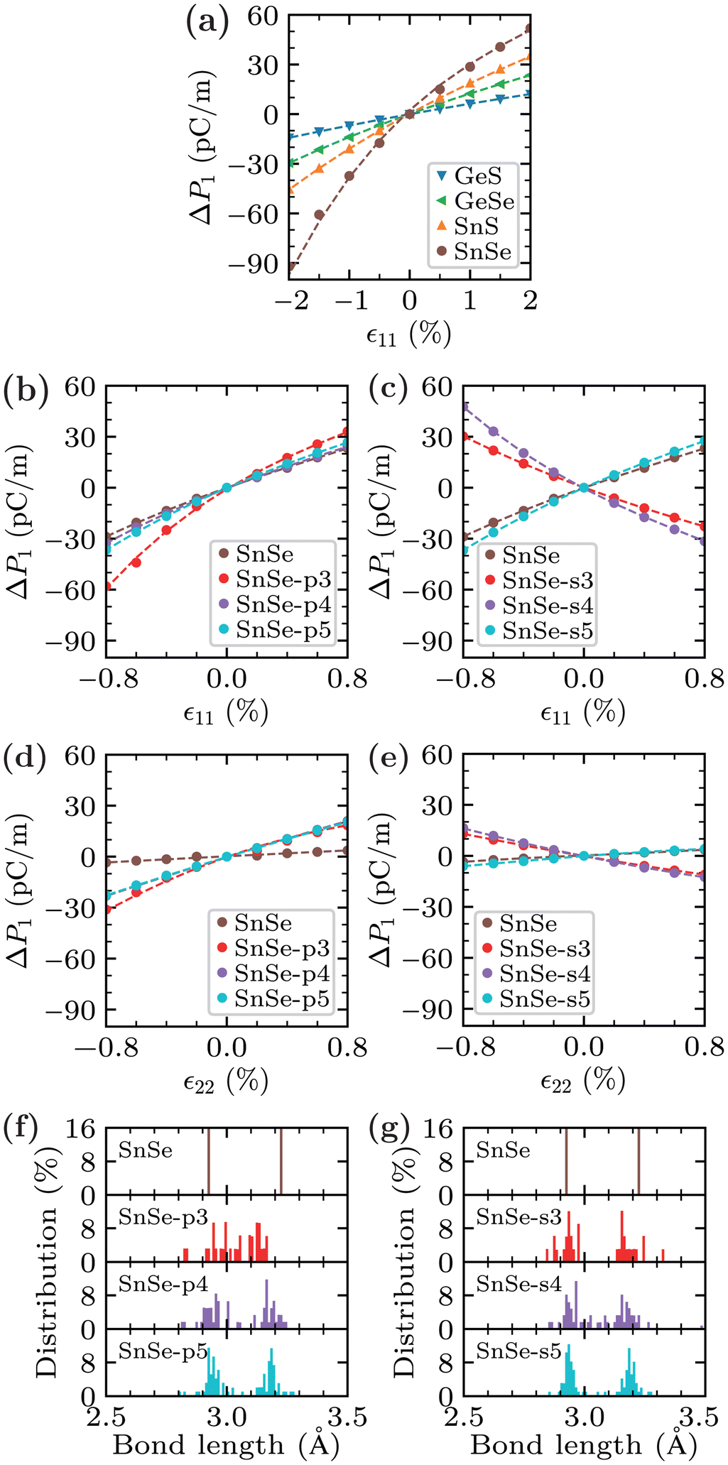 | ||
| Fig. 3 Normalized polarization ΔP1 = P1(εjk) − P1(0) under strain in (a) pristine monolayer GeS, GeSe, SnS, and SnSe as well as in monolayer SnSe with (b) and (d) Sn–Se and (c) and (e) Se vacancies. (f) and (g) Histograms of the intralayer bond lengths (ls and lw). | ||
The presence of vacancies can significantly affect the charge density distribution and, thus, the charge transfer. We consider vacancy densities of 5.5% (SnSe-p3), 3.1% (SnSe-p4), 2.0% (SnSe-p5), 2.2% (SnSe-s3), 1.5% (SnSe-s4), and 1.0% (SnSe-s5). Table 1 shows that the piezoelectric coefficients of SnSe-p4 and SnSe-p5 are a bit higher than those of pristine monolayer SnSe, whereas those of SnSe-p3 are significantly higher (60% for e111 and 433% for e122). To explain this effect and the modifications of ΔP1 in the presence of Sn–Se vacancies, see Fig. 3(b) and (d), particularly the almost identical curves of SnSe-p4 and SnSe-p5 in contrast to that of SnSe-p3, we show in Fig. 3(f) histograms of the intralayer bond lengths (ls and lw) in the supercells. As expected, pristine SnSe shows two peaks of equal weight at 2.9 Å and 3.2 Å, while Sn–Se vacancies smear out the distribution. The two original peaks can still be recognised in the cases of SnSe-p4 and SnSe-p5 in contrast to the case of SnSe-p3, demonstrating that ls and lw, on average, are less similar for SnSe-p4 and SnSe-p5 than for SnSe-p3. Therefore, there is a strong correlation between the bond length disparity and the piezoelectric coefficients. Substantial structural relaxation in the cases of SnSe-s3 and SnSe-s4 results in negative e111 and e122. SnSe-s4 shows the highest |e111| and |e122| among the Se vacancies, see Fig. 3(c) and (e), because the distribution of the intralayer bond lengths is smeared out most, see Fig. 3(g). Thus, the bond length disparity and piezoelectric coefficients are strongly correlated also in the case of Se vacancies. Reducing the bond length disparity, consequently, is an effective route to enhance the piezoelectric response in monolayer group IV monochalcogenides.
4. Conclusion
Our comprehensive investigation of the charge redistribution in monolayer group IV monochalcogenides under strain fully explains the trends of the piezoelectricity obtained in this family of materials. Charge transfer between the strong and weak intralayer bonds turns out to be the root cause of the piezoelectricity. Our results also suggest that the piezoelectric response is enhanced both by compressive strain and the presence of Sn–Se and Se vacancies, providing strategies to improve electro-mechanical devices.Data availability
The data supporting this study are included in the article.Conflicts of interest
There are no conflicts to declare.Acknowledgements
We are grateful to Mohammed Ghadiyali and Shubham Tyagi for engaging discussions. The research reported in this publication was supported by funding from King Abdullah University of Science and Technology (KAUST). For computer time, this research used the resources of the Supercomputing Laboratory at KAUST.References
- Y. Nemirovsky, A. Nemirovsky, P. Muralt and N. Setter, Design of novel thin-film piezoelectric accelerometer, Sens. Actuators, A, 1996, 56, 239 CrossRef CAS.
- S. Tadigadapa and K. Mateti, Piezoelectric MEMS sensors: State-of-the-art and perspectives, Meas. Sci. Technol., 2009, 20, 092001 CrossRef.
- H. Bhugra and G. Piazza, Piezoelectric MEMS resonators, Springer, Berlin, 2017 Search PubMed.
- M. Pohanka, Overview of piezoelectric biosensors, immunosensors and DNA sensors and their applications, Mater., 2018, 11, 448 Search PubMed.
- D. Hu, M. Yao, Y. Fan, C. Ma, M. Fan and M. Liu, Strategies to achieve high performance piezoelectric nanogenerators, Nano Energy, 2019, 55, 288 Search PubMed.
- N. Sezer and M. Koç, A comprehensive review on the state-of-the-art of piezoelectric energy harvesting, Nano Energy, 2021, 80, 105567 CrossRef CAS.
- X. Gao, J. Yang, J. Wu, X. Xin, Z. Li, X. Yuan, X. Shen and S. Dong, Piezoelectric actuators and motors: Materials, designs, and applications, Adv. Mater. Technol., 2019, 5, 1900716 CrossRef.
- A. Zaszczynska, P. Sajkiewicz and A. Gradys, Piezoelectric scaffolds as smart materials for neural tissue engineering, Polymers, 2020, 12, 161 CrossRef CAS PubMed.
- C. Yang, J. Ji, Y. Lv, Z. Li and D. Luo, Application of piezoelectric material and devices in bone regeneration, Nanomater, 2022, 12, 4386 CrossRef CAS.
- W. Wu, L. Wang, Y. Li, F. Zhang, L. Lin, S. Niu, D. Chenet, X. Zhang, Y. Hao, T. F. Heinz, J. Hone and Z. L. Wang, Piezoelectricity of single-atomic-layer MoS2 for energy conversion and piezotronics, Nature, 2014, 514, 470 CrossRef CAS PubMed.
- H. Zhu, Y. Wang, J. Xiao, M. Liu, S. Xiong, Z. J. Wong, Z. Ye, Y. Ye, X. Yin and X. Zhang, Observation of piezoelectricity in free-standing monolayer MoS2, Nat. Nanotechnol., 2014, 10, 151 CrossRef.
- J. Zhang and S. Meguid, Piezoelectricity of 2D nanomaterials: Characterization, properties, and applications, Semicond. Sci. Technol., 2017, 32, 043006 CrossRef.
- M. N. Blonsky, H. L. Zhuang, A. K. Singh and R. G. Hennig, Ab Initio prediction of piezoelectricity in two-dimensional materials, ACS Nano, 2015, 9, 9885 CrossRef CAS.
- W. Li and J. Li, Piezoelectricity in two-dimensional group III monochalcogenides, Nano Res., 2015, 8, 3796 CrossRef CAS.
- R. Fei, W. Li, J. Li and L. Yang, Giant piezoelectricity of monolayer group IV monochalcogenides: SnSe, SnS, GeSe, and GeS, Appl. Phys. Lett., 2015, 107, 173104 CrossRef.
- L. C. Gomes, A. Carvalho and A. H. Castro Neto, Enhanced piezoelectricity and modified dielectric screening of two-dimensional group IV monochalcogenides, Phys. Rev. B: Condens. Matter Mater. Phys., 2015, 92, 214103 CrossRef.
- Y. Dai, X. Zhang, Y. Cui, M. Li, Y. Luo, F. Jiang, R. Zhao and Y. Huang, Theoretical insights into strong intrinsic piezoelectricity of blue-phosphorus-like group IV monochalcogenides, Nano Res., 2021, 15, 209 CrossRef.
- Y. Zhou, D. Wu, Y. Zhu, Y. Cho, Q. He, X. Yang, K. Herrera, Z. Chu, Y. Han, M. C. Downer, H. Peng and K. Lai, Out-of-plane piezoelectricity and ferroelectricity in layered α-In2Se3 nanoflakes, Nano Lett., 2017, 17, 5508 CrossRef CAS PubMed.
- M. T. Ong and E. J. Reed, Engineered piezoelectricity in graphene, ACS Nano, 2012, 6, 1387 CrossRef CAS.
- S. Chandratre and P. Sharma, Coaxing graphene to be piezoelectric, Appl. Phys. Lett., 2012, 100, 023114 CrossRef.
- F. Ahmadpoor and P. Sharma, Flexoelectricity in two-dimensional crystalline and biological membranes, Nanoscale, 2015, 7, 16555 RSC.
- Y. Gao, L. Zhang, G. Yao and H. Wang, Unique mechanical responses of layered phosphoruslike group-IV monochalcogenides, J. Appl. Phys, 2018, 125, 082519 CrossRef.
- F. Li, H. Chen, L. Xu, F. Zhang, P. Yin, T. Yang, T. Shen, J. Qi, Y. Zhang, D. Li and Y. Ge, Defect engineering in ultrathin SnSe nanosheets for high-performance optoelectronic applications, ACS Appl. Mater. Interfaces, 2021, 13, 33226 CrossRef CAS.
- G. Kresse and D. Joubert, From ultrasoft pseudopotentials to the projector augmented-wave method, Phys. Rev. B: Condens. Matter Mater. Phys., 1999, 59, 1758 CrossRef CAS.
- R. D. King-Smith and D. Vanderbilt, Theory of polarization of crystalline solids, Phys. Rev. B: Condens. Matter Mater. Phys., 1993, 47, 1651 CrossRef CAS PubMed.
- N. A. Spaldin, A beginner's guide to the modern theory of polarization, J. Solid State Chem., 2012, 195, 2 CrossRef CAS.
- D. Vanderbilt, Berry-phase theory of proper piezoelectric response, J. Phys. Chem. Solids, 2000, 61, 147 CrossRef CAS.
- S. Nag, A. Saini, R. Singh and R. Kumar, Influence of vacancy defects on the thermoelectric performance of SnSe sheet, Phys. E, 2021, 134, 114814 CrossRef CAS.
- Y. Guo, H. Zhu and Q. Wang, Piezoelectric effects in surface-engineered two-dimensional group III nitrides, ACS Appl. Mater. Interfaces, 2018, 11, 1033 CrossRef.
- N. I. Atallah, M. E. Kemary, F. Pascale and K. E. E. Kelany, Extraordinary piezoelectric effect induced in two-dimensional rare earth monochalcogenides via reducing system dimensionality, J. Materiomics, 2023, 9, 72 CrossRef.
- Y. Chen, J. Liu, J. Yu, Y. Guo and Q. Sun, Symmetry-breaking induced large piezoelectricity in Janus tellurene materials, Phys. Chem. Chem. Phys., 2019, 21, 1207 RSC.
- X. Wang, W. Shi and J. Wan, Enhanced piezoelectric effect in MoS2 and surface-engineered GaN bilayer, J. Appl. Phys., 2021, 130, 015113 CrossRef CAS.
- N. Ghobadi, S. G. Rudi and S. S. Amiri, Electronic, spintronic, and piezoelectric properties of new Janus ZnAXY (A = Si, Ge, Sn, and X, Y = S, Se, Te) monolayers, Phys. Rev. B, 2023, 107, 075443 CrossRef CAS.
- Y. Guo, J. Zhou, H. Xie, Y. Chen and Q. Wang, Screening transition metal-based polar pentagonal monolayers with large piezoelectricity and shift current, npj Comput. Mater., 2022, 8, 40 CrossRef CAS.
- J. George, G. Petretto, A. Naik, M. Esters, A. J. Jackson, R. Nelson, R. Dronskowski, G. M. Rignanese and G. Hautier, Automated bonding analysis with crystal orbital Hamilton populations, ChemPlusChem, 2022, 87, e202200123 CrossRef CAS PubMed.
| This journal is © The Royal Society of Chemistry 2025 |