
 Open Access Article
 This Open Access Article is licensed under a
 Creative Commons Attribution 3.0 Unported Licence
Preparation and interfacial engineering of sputtered electrolytes for thin film oxygen ion batteries†
Alexander
Schmid
 *,
Tobias M.
Huber
,
Florian
Karbus
,
Maximillian
Weiss
,
Andreas
Limbeck
and
Jürgen
Fleig
*,
Tobias M.
Huber
,
Florian
Karbus
,
Maximillian
Weiss
,
Andreas
Limbeck
and
Jürgen
Fleig
Institute of Chemical Technologies and Analytics, TU Wien, Getreidemarkt 9, Vienna, A-1060, Austria. E-mail: alexander.e164.schmid@tuwien.ac.at
First published on 25th June 2025
Abstract
This study investigates the structural, chemical, and electrochemical properties of yttria-stabilized zirconia (YSZ) thin film electrolytes for thin film oxygen ion batteries (OIB), prepared by reactive DC magnetron sputtering. The films were deposited on various electrode materials, including platinum and mixed ionic electronic conducting (MIEC) perovskite oxides, with and without gadolinia-doped ceria (GDC) buffer layers. Characterization techniques such as scanning electron microscopy, laser ablation inductively coupled plasma mass spectrometry, X-ray fluorescence spectroscopy and X-ray diffractometry were employed to analyze the microstructural and chemical properties of the films. Electrochemical impedance spectroscopy and galvanostatic charge–discharge cycling were used to evaluate the ionic conductivity and interfacial resistance of the YSZ films. The results demonstrate that the YSZ films exhibit a dense, polycrystalline structure with a highly columnar grain morphology and a chemical composition close to the desired stoichiometry. The ionic conductivity of the films is slightly lower than that of single crystal YSZ, with an activation energy of approximately 1.09 eV. The introduction of GDC buffer layers significantly reduces the interfacial resistance of YSZ grown on MIEC perovskite films, thereby lowering the effective electrolyte resistance by up to 75%. Thin film electrolyte OIBs were prepared and operated at 250 °C, and substantiated the performance increase by interfacial engineering, i.e. the introduction of GDC buffer layers.
Introduction
Solid oxide electrochemistry is key for solid oxide fuel cells (SOFCs), solid oxide electrolysis cells1–4 or (photo) electrochemical water or CO2 splitting5–7 and is thus a cornerstone of efficient energy conversion and storage. More recently, a new type of solid oxide electrochemical cell, the oxygen ion battery (OIB), has emerged.8–11 OIBs exploit the variable oxygen stoichiometry existing in many mixed ionic electronic conducting (MIEC) oxides for electrochemical energy storage. Analogous to lithium ion batteries, two MIEC oxide electrodes are separated by an oxide ion conducting, but electronically insulating electrolyte, allowing the transfer of oxygen from one electrode to the other by an applied current (charging), or the retrieval of stored electrical energy (discharging) by the reverse process. OIBs allow operation at elevated temperatures (250–500 °C), which together with their non-flammability makes them ideally suited for deployment in harsh industrial environments. Miniaturization of such cells, e.g. as thin film devices, may thus be highly attractive for application in small, autonomous devices, e.g. in industrial internet of things sensor nodes.Similar to SOFCs, the electrolyte is a critical component in OIBs, as it requires a low ion transport resistance while still ensuring electronic insulation of the two storage electrodes. In the field of SOFCs, much effort is directed at miniaturizing the electrolyte, and different thin film deposition routes such as pulsed laser deposition (PLD),12,13 sputtering,14,15 sol–gel spin coating16 and screen printing17 are explored. This study focuses on the preparation and interfacial engineering of sputtered yttria-stabilized zirconia (YSZ) thin film electrolytes for thin film OIBs. Reactive DC magnetron sputtering was employed to deposit YSZ thin films electrolytes, allowing the fabrication of dense, polycrystalline electrolyte thin films.
The primary objective of this study is to demonstrate the viability of very thin (200 nm) electrolyte films for applications in OIBs. In such thin film systems, interfaces play an especially important role and thus a further aim was to engineer the electrolyte/electrode interface in order to further improve electrolyte performance. Specifically, from high temperature SOFCs research it is known that YSZ and perovskite electrode materials containing La or Sr react at high temperatures to form resistive secondary phases, which can be avoided by introducing an interlayer of gadolinia-doped ceria (GDC).18–21 In this study we apply this approach in the form of an ultrathin (5 nm) buffer layer also grown by sputter deposition. Electrochemical impedance spectroscopy (EIS) on model YSZ thin film systems and on full OIB thin film cells was used to investigate the resistive contributions of the YSZ film and the interface. Additionally, galvanostatic charge/discharge cycle experiments were performed on the OIB cells.
The results demonstrate the viability of thin film OIBs with sputtered YSZ thin film electrolytes. Furthermore, they show that the GDC buffer layers significantly improve the effective electrolyte resistance by eliminating the interfacial resistance, highlighting the importance of interfacial engineering in the development of high-performance thin film OIBs.
Experimental
Sample preparation
Three different sample types were used in this study: YSZ layers between two Pt thin film electrodes, YSZ films directly between two MIEC perovskite electrodes—La0.6Sr0.4FeO3−δ (LSF) and La0.5Sr0.5Cr0.2Mn0.8O3−δ (LSCrMn)—and YSZ layers between two MIEC perovskite electrodes with GDC buffer layers between YSZ and perovskite. For the two latter sample types, the LSF and LSCrMn electrodes were contacted by Pt thin film electrodes and isolated from the atmosphere by a second, thicker YSZ film. In all three sample architectures, the effective electrolyte area, i.e. the area directly between electrodes, was 7 × 7 mm2.Furthermore, they comprised an auxiliary porous LaxSr1−xCoO3−δ electrode on the bottom side of the substrate. Fig. 1 shows cross-sections of the three sample types.
 | ||
| Fig. 1 Schematic cross-sections of the sample architectures used in this study. YSZ electrolyte films were grown between two Pt films (a), between two MIEC oxide films (b) or between two MIEC oxide films with additional GDC buffer layers (c). | ||
Samples were prepared on 10 × 10 × 0.5 mm3 YSZ single crystal substrates (Y2O3 molar fraction of 9% Crystek, Germany), polished on the square sides and oriented in (100) direction. Substrates were cleaned by sonicating them in Extran (Merck, Germany) twice, followed by sonication in twice distilled water and ethanol (99.93%, VWR chemicals, Germany). Afterwards, substrates were annealed in air at 1200 °C for 2 h.
Pt films were prepared by DC magnetron sputtering in Ar atmosphere at 2 Pa using a current of 100 mA. Substrates were heated to 600 °C during deposition to improve mechanical and thermal stability of the Pt layers. Patterning of the Pt thin films was done by photo-lithography and ion beam etching to obtain grids with 15 μm strip width and 35 μm mesh size.
MIEC perovskite films were prepared by PLD using the parameters listed in Table 1. Targets for PLD were prepared from powders synthesized by Pechini's method by pressing and sintering in air at 1200 °C for 12 h.8 PLD was chosen for fabrication of the perovskite electrodes, as it allows deposition of ceramic layers with complex stoichiometry (up to 4 cations in our case). For industrial scale fabrication, sputter deposition would be preferable, but may require considerable effort in process tuning to achieve complex stoichiometries.
| LSF | LSCrMn | LSC (porous) | ||
|---|---|---|---|---|
| Laser pulses | 43 | 31 | 25 | (nm) |
| Laser fluence | 1.1 | 1.1 | 1.4 | (J cm−2) |
| Pulse frequency | 10 | 10 | 5 | (Hz) |
| Oxygen pressure | 4 | 1.5 | 15 | (Pa) |
| Substrate temperature | 600 | 700 | 450 | (°C) |
| Target to substrate distance | 6 | 6 | 6 | (cm) |
YSZ thin films were prepared by reactive DC magnetron sputtering from a Zr/Y (Y mass fraction of 15%) metal target (99.9%, MSE Supplies, USA) in an atmosphere of 0.35 Pa O2 and 1.05 Pa Ar (99.999%, Air Liquide). The power was held constant at 120 W (5.9 W cm−2), resulting in a voltage of 300 to 320 V and a current of 390 to 410 mA (19 to 20 mA cm−2). Deposition rates were typically about 67 pm s−1. Gd0.1Ce0.9O1.95 (GDC10) buffer layers were deposited by RF magnetron sputtering from a ceramic GDC10 target, made by pressing and sintering from GDC10 powder (Treibacher, Austria). The atmosphere was the same as for the YSZ deposition and the sputter power was again held constant at 120 W. Deposition rates were about 98 pm s−1 and thus higher than for YSZ. For both materials, the substrate was heated to 600 °C during depositions, and the target to substrate distance was 6 cm. To ensure electronically insulting films and avoid electronic conduction paths caused by pinholes, particle contaminants or other film imperfections, YSZ films were sputtered in two steps. After the first half of the deposition, samples were cooled to room temperature, taken out of the chamber and cleaned by sonicating in ethanol. Then the samples were reheated, and the second half was deposited. This two-step process resulted in a roughly 90% yield of samples without any short circuits between the electrodes, a significant improvement over the approximately 10% yield achieved with a single-step deposition.
Alumina shadow masks were used for all thin film depositions to achieve an overlapping layer structure, resulting in electronic insulation of the individual electrodes. To minimize stresses caused by different thermal expansion of the individual film, heating and cooling rates were limited to 15 °C min−1 for all depositions.
Structural and chemical characterization
Grazing incidence X-ray diffractometry (XRD) measurements were done on an Empyrean multipurpose diffractometer (PANalytical, Germany). A Cu-tube operating at 45 kV and 40 mA was used as source, providing wavelengths of 154.06 pm (Cu K-α-1) and 154.44 pm (Cu K-α-2). An incident angle (ω) of 3° was used, and the diffraction angle (2θ) was scanned from 10 to 90° with a step size of 0.02° and a measurement time of 1 s per step. Scanning electron microscopy (SEM) images were taken on an FEI Quanta 250 FEG.Laser ablation (LA)-inductively coupled plasma (ICP)-mass spectrometry (MS) measurements were performed on an iCap TQ (Thermo Fischer) triple quad ICP-MS system coupled to an imageGEO193 (Elemental Scientific Lasers (Bozeman, MT, USA)) laser ablation system operating at 193 nm wavelength using an excimer laser, equipped with a “TwoVol3 ablation chamber through a PTFE Tubing and Dual Concentric Injector” interface. The system is tuned on a daily basis for maximum. 115In sensitivity and lowest ThO/Th ratio using a NIST612 glass standard. Laser ablation was performed with 5 line scans of 1 mm length distributed over the sample using 1 J cm−2 laser fluence, non-overlapping spots with a size of 5 × 5 μm2, 100 Hz laser frequency and 500 μm s−1 scan speed. The signal was quantified using a YSZ single crystal (Crystek) with a known dopant concentration (9 mol% Y2O3) as one point standard. X-ray fluorescence spectroscopy (XRF) measurements were performed on a PANalytical Axios advance wavelength dispersive spectrometer equipped with a rhodium tube. The composition was quantified using the PANalytical Omnian standards with the respective routine in the Omnian software.
Electrochemical characterization
For electrochemical characterization, the samples were placed in an alumina sample holder. The bottom reference electrode was contacted via a Pt mesh and the Pt electrodes and current collectors on the top side were contacted by Pt needles. The sample holder was mounted inside a sealed fused silica tube and placed inside a tube furnace. The measurement atmosphere was 1% O2 in N2 (99.999%, Air Liquide) and the temperature was measured via a thermocouple in proximity to the sample.After first heating up the sample to the measurement temperature, an equilibration step was performed by shorting together all electrodes of the sample for at least 6 h. This was done to ensure that the oxygen chemical potential of all electrodes (especially the MIEC electrodes not exposed to the atmosphere) was equal to the atmospheric oxygen chemical potential. To minimize stresses caused by different thermal expansion of the individual films, heating and cooling rates were limited to 15 °C min−1.
Impedance spectra were recorded using an SP-200 potentiostat (Biologic, France) between 150–400 °C in single sine mode using an AC amplitude between 10 mV and 50 mV. A frequency range of 106 to 10−1 Hz was recorded with 12 points per decade and each frequency point was measured for at least one full period of the sinusoidal voltage. At each temperature, six consecutive spectra were recorded to verify system stability and each temperature ramp was repeated multiple times in increasing and decreasing temperature direction.
For DC experiments, also performed with the SP-200 potentiostat, first the LSF electrode was reduced by applying a constant current of 1 μA between it and the auxiliary air electrode. This step was necessary because after thin film deposition and equilibration, both MIEC electrodes are virtually fully oxidized, whereas battery operation requires one to be oxidized, and the other to be reduced. Oxidized here means that the Sr doping is almost entirely compensated by Mn4+ in LSCrMn and by (nominally) Fe4+ in LSF. The potential of the LSF electrode during this preconditioning was measured relative to the LSCrMn electrode, which, after the initial equilibration step, was at atmospheric oxygen chemical potential. In total, the transferred charge corresponds to a complete reduction of all iron in LSF to Fe3+, leading to a final potential of the LSF electrode of −0.8 V vs. O2. After this preconditioning step, the cell was cycled by applying a constant positive current between the LSF and LSCrMn electrodes until the cell voltage reached 1 V, followed by a negative current until the cell voltage reached 0 V. A detailed, mechanistic explanation of these conditioning, charge and discharge phases is given in previous publications.8,9 The charge/discharge cycle was repeated between five and one hundred times, depending on current, to keep experiment runtimes reasonable. Currents from 10 to 500 μA were used at a temperature of 250 °C.
Structural and chemical properties
Fig. 2 shows top view and cross-section SEM images of a YSZ film grown on a Pt layer. From the top view (Fig. 2a) a polycrystalline film morphology is visible with a very narrow grain size distribution around 77 ± 4 nm. The film surface appears very homogenous with no apparent defects like voids, cracks or pinholes. The cross-section image (Fig. 2b) reveals that the films grow fully dense, with a highly columnar grain structure. | ||
| Fig. 2 SEM top view (a) and cross-section (b) images of a YSZ film grown on a Pt film. | ||
Fig. 3 shows a grazing incidence diffractogram of a YSZ thin film grown on a Pt film. All peaks can be assigned either to the YSZ film, or to the underlying Pt film electrode, confirming a phase pure, polycrystalline film growth.
 | ||
| Fig. 3 Gracing incidence diffractogram of a YSZ thin film grown on a Pt film, recorded using an incidence angle of 3°. | ||
The chemical composition of the sputtered YSZ films was determined by LA-ICP-MS and by XRF. Table 2 lists the obtained molar Y to Zr ratios, together with reference data measured on a single crystal. Data obtained by both XRF and LA-ICP-MS are in very good agreement and confirm that the stoichiometry of the sputtered YSZ thin film is close to the desired composition.
| XRF | LA-ICP-MS | Nominal | |
|---|---|---|---|
| Sputtered thin film | 0.21 ± 0.04 | 0.20 ± 0.07 | 0.20 |
| Crystek single crystal | 0.21 ± 0.01 | 0.200 ± 0.004 | 0.20 |
Impedance spectra of YSZ films grown on Pt
In a first experiment, the sputtered YSZ films were contacted between two Pt electrodes as shown in Fig. 1a. Fig. 4a to e display impedance spectra of such a cell at various temperatures. The spectra consist of a high frequency intercept, a medium frequency distorted semicircle and a constant slope feature at low frequencies. The high frequency intercept is attributed to the wiring and contact resistance and possibly also includes contributions from the in-plane electron transport in the Pt thin film electrodes. This is consistent with its weakly positive temperature dependence. The low frequency feature is attributed to the electrode reaction. | ||
| Fig. 4 Impedance spectra of sputtered YSZ films, contacted between two Pt film electrodes (a to e). Symbols indicate measured data points, lines are fits to the equivalent circuit model shown in (f). | ||
The mid-frequency semicircle is attributed to the cross-plane ion transport resistance of the YSZ film, consistent with its strongly negative temperature dependence. Typically, for polycrystalline YSZ, both grain and grain boundary resistances may contribute to the effective ionic resistance, often showing as two distinct semicircles in the Nyquist plot.22–24 However, in contrast to macroscopic bulk samples, here, the columnar growth of the film leads to only very few grain boundaries being oriented in-plane, i.e. normal to the direction of current flow. Thus, no separate grain boundary semicircle is visible, and the medium frequency feature corresponds predominantly to the grain transport resistance.
In accordance with literature on similar or related systems, these spectra were parametrized via the equivalent circuit model shown in Fig. 4f.25–28 It consists of an inductor in series with a resistor, which account for the high frequency intercept, a constant phase element (CPE), which accounts for the low frequency electrode feature and a parallel R-CPE element which describes the YSZ ion transport resistance and the dielectric capacitance. The CPEs were used to model imperfect capacitances with impedance ZCPE = T−1(iω)−P; a P value of 1 corresponds to an ideal capacitor.29 Estimated fit errors were typically between 1% and 5% for all fit parameters.
The YSZ ion transport resistance and the dielectric capacitance obtained from the equivalent circuit model were normalized to the YSZ thickness (d) and the area between the two Pt layers (A) according to
 | (1) |
 | (2) |
Impedance spectra of YSZ films grown on MIEC films
In a second experiment, YSZ films were grown between two MIEC thin film electrodes, both with and without GDC buffer layers as shown in Fig. 1b and c. Fig. 5a to e show impedance spectra of these cells, measured between the LSF and LSCrMn electrodes at different temperatures. These spectra are qualitatively very similar to the ones of YSZ films between two Pt contacts, except for one distinct difference: spectra of samples without GDC buffer layers present an additional feature between the medium frequency semicircle and the low frequency electrode feature. This additional feature is close to a 45° slope, with a slight curvature; the curvature is more pronounced at lower temperatures.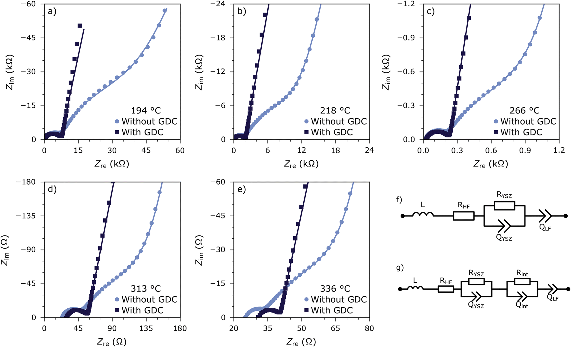 | ||
| Fig. 5 Impedance spectra of sputtered YSZ films between two MIEC electrode films (a to e). Symbols indicate measured data points, lines are fits to the equivalent circuit model shown in (f) and (g) for the spectra of samples without and with buffer layers, respectively. | ||
Since this additional feature appears only in samples containing a YSZ/perovskite interface, it is likely associated with processes occurring at that interface. In SOFCs sintered at high temperatures (e.g. above 1000 °C), such interface resistances are frequently observed and are attributed to an interfacial reaction between perovskite electrode and YSZ electrolyte, leading to the formation of highly resistive phases such as La2Zr2O7 and SrZrO3.18,21,31–34
However, similar interfacial resistances are also observed in systems where thin-film perovskite electrodes are deposited onto YSZ substrates via physical vapor deposition (PVD) techniques at much lower temperatures (typically 500–800 °C).27,28,35,36
This suggests that the underlying mechanism responsible for the interfacial resistance in high-temperature SOFCs may also apply to thin-film systems, despite the differences in processing conditions. In addition, other factors—such as cation interdiffusion without the formation of a novel phase—may also contribute to the observed resistance in our case.
Supporting this interpretation, similar interfacial resistance features were found in cells consisting of PLD-grown perovskite electrodes on YSZ single-crystal substrates. Notably, both LSF and LSCrMn formed resistive interfaces with YSZ, as discussed in more detail in the ESI.†
Notably, the interfacial feature is absent in our cells that include a thin GDC buffer layer between the perovskite and YSZ. Similar to its role in conventional high-temperature SOFCs, the GDC layer likely acts as a barrier that inhibits interfacial interdiffusion or reactions, and its inclusion effectively eliminates the additional resistance in our thin-film cells as well.18–20
Spectra of samples with GDC buffer layer were quantified with the same equivalent circuit as YSZ films between two Pt films, see Fig. 5f. For the spectra of samples without buffer layer, an additional R-CPE element was added to account for this additional interfacial feature, see Fig. 5g. Fit errors were again between 1% and 5% for all parameters except the interfacial resistance Rint, where it was 10 to 30%. The P value of the CPE Qint was between 0.7 and 0.85, i.e. somewhat intermediary between an ideal 45° slope with a P value of 0.5 and an ideal semicircle with P value of 1. The YSZ transport resistances were again normalized to the thin film dimensions, and the resulting ionic conductivities are shown in Fig. 6.
 | ||
| Fig. 6 Ionic conductivity of YSZ thin films prepared by reactive DC sputtering on Pt electrodes and on MIEC perovskite electrodes with and without an interfacial GDC buffer layer. The ionic conductivity of a YSZ single crystal is shown for reference.25 | ||
Ionic conductivity and interfacial resistance
The ionic conductivity extracted from the impedance spectra is shown in Fig. 6 as a function of temperature together with literature data for bulk single crystals of similar chemical composition.25 For YSZ films grown on Pt electrodes, the conductivity is lower than that of the singly crystal by a factor of 2.5. The deviation may in part be caused by minor resistive contributions from grain boundaries, but may also depend on the specific Y distribution which is a consequence of the thermal history of the YSZ film.25 A distinct Arrhenius-type relation is evident, with an activation energy of 1.09 ± 0.004 eV, which is very close to the value of 1.14 eV for the single crystal in this temperature regime.For samples with MIEC electrodes, the ionic conductivity of the YSZ films—with or without buffer layer—is virtually identical over the entire temperature range, supporting our separation into YSZ transport and interface resistance. Compared to the films grown on Pt, the conductivity is slightly lower by about a factor of 1.5, and this might be due to minor differences in film growth on Pt and on MIEC perovskite. The activation energies of 1.11 ± 0.01 eV for samples without GDC buffer and 1.13 ± 0.01 eV for sample with buffer, on the other hand, are again very close to that of that films grown between Pt layers (1.09 ± 0.004 eV) and to the single crystal value of 1.14 eV.25 Also the relative permittivity extracted from the medium frequency feature, 40 to 47 is again consistent with that of YSZ.22,30 Please note: the ionic transport resistance of the buffer layers themselves does not contribute notably to the electrolyte resistance, as the thickness of the buffer layers (approximately 5 nm, estimated from deposition time and deposition rate) is very low compared to that of YSZ layers (200 nm) and furthermore, GDC is generally more conductive than YSZ.37
Fig. 7 displays the YSZ ionic transport and interfacial resistances of the YSZ films with and without buffer layers. Since the thickness of the interfacial layer is unknown, the resistances obtained from the equivalent circuit model fits were normalized to the film area. The YSZ transport resistance is again virtually identical for samples with and without the additional GDC buffer layer. The interfacial resistance present in samples without buffer layer is larger than the YSZ transport resistance by a factor of 2.6 to 10.6 depending on temperature. Furthermore, it is more strongly thermally activated with an activation energy of 1.26 ± 0.03 eV compared to the YSZ transport with 1.11 to 1.13 eV. Additional samples with increased GDC thickness showed the same suppression of interfacial resistance, indicating that the effect is robust within respect to the GDC thickness. In systems with very thin electrolytes, such as these, the interfacial resistance thus dominates the effective electrolyte resistance. This highlights again the importance of adequately engineering the electrolyte-electrode interface by preventing the formation of low conductivity zirconates through the introduction of a buffer layer.
 | ||
| Fig. 7 Area specific YSZ transport and interfacial resistances as a function of temperature. | ||
Charge voltage curves
Galvanostatic charge and discharge cycling experiments were performed to complement the EIS measurements and demonstrate the viability of sputtered thin film electrolytes for low temperature thin film OIB cells. Fig. 8 displays exemplary charge vs. voltage curves recorded on samples with and without GDC buffer layer over multiple consecutive charge–discharge cycles.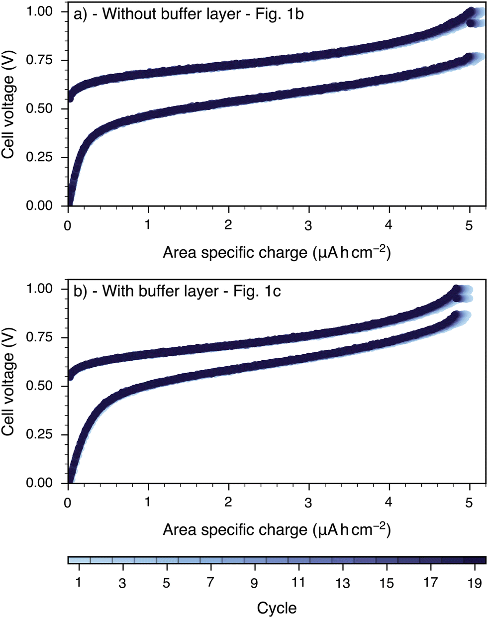 | ||
| Fig. 8 Voltage vs. charge during charging as discharging for cells without (a) and with (b) GDC buffer layer recorded galvanostatically with a current density of 102 μA cm−2 at 250 °C. | ||
A detailed mechanistic description of such OIB cells is given in a previous publication,8 here we only repeat the basic operation principle. During charging, oxygen ions are pumped from the LSCrMn electrode to the LSF electrode by an externally applied current, and thereby LSCrMn gets reduced, while LSF gets oxidized. During discharging, the reverse process occurs. Notably, this is a pure solid state process, without any involvement of the gas phase. Both cells exhibit stable, reversible cycling behavior with high Coulomb efficiency (>99.5%). The slight capacity decrease notable in Fig. 8 is reversible through a regeneration step.8,9 Including such steps, the cells were cycled for 2000 cycles without any signs of irreversible degradation.
However, one distinct difference is again present: for the cell without GDC buffer layers, the charging voltage is higher and the discharging voltage is lower, compared to the cell with buffer layers, i.e. overpotential losses are higher without buffer layers. This is consistent with the presence of the additional interfacial resistance found in the EIS experiments.
From these curves, the overpotential was estimated by subtracting the voltages during charging and discharging at equal state of charge, assuming that the overpotential is the same in both directions, i.e.
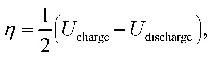 | (3) |
| UOC = Ucharge − η = Udischarge + η, | (4) |
 | ||
| Fig. 9 Overpotential and open circuit voltage extracted from charge and discharge voltages in Fig. 8 as a function of state-of-charge for cells without (a) and with (b) GDC buffer layers. | ||
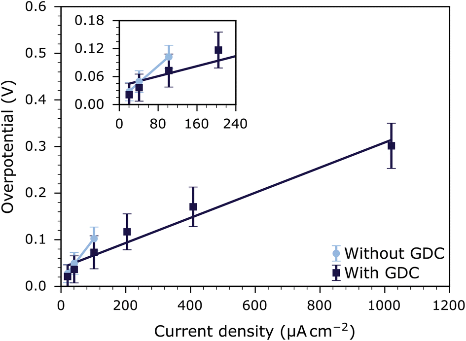 | ||
| Fig. 10 Overpotential averaged over the entire state-of-charge range as function of current density at 250 °C for cells with and without GDC buffer layer. Markers denote data points, lines indicate linear regression fits. The inset shows a magnification of the low current regime. | ||
Despite some scattering, a linear relation between current and overpotential is evident, corresponding to ohmic behavior. The resistances obtained from linear regression fits are 269 ± 26 Ω cm2 and 906 ± 41 Ω cm2, for cells with and without buffer layer, respectively. These values fit very well to predictions based on the electrolyte and interface resistances determined by EIS (193 Ω cm2 and 1020 Ω cm2). Altogether, these proof-of-concept cells demonstrate the viability of sputtered YSZ electrolytes for thin film OIBs, and highlight the importance of interfacial modification.
Conclusion
YSZ films were prepared using reactive DC magnetron sputtering and characterized using a combination of SEM, XRD, LA-ICP-MS, and XRF techniques. The electrochemical performance of the films was evaluated using electrochemical impedance spectroscopy and galvanostatic charge–discharge cycling. The YSZ layers exhibit a dense, polycrystalline structure with a highly columnar grain morphology. The chemical composition of the films was confirmed to be close to the desired stoichiometry, with molar Y to Zr ratios consistent with reference single crystal data. The ionic conductivity of the YSZ films was found to be only slightly lower than that of single crystal YSZ. However, the activation energy for ionic conduction was very close to the literature value of single crystalline YSZ, indicating that the dominant conduction mechanism is similar, i.e. grain conduction.The ionic conductivity of YSZ films grown on MIEC electrodes was very close to that of the films grown on Pt, but the activation energies were again comparable. However, the impedance spectra of such films showed an additional feature that could be attributed to interfacial resistance. This additional resistive contribution was effectively mitigated by the introduction of a GDC buffer layer.
YSZ thin films were used as electrolytes in thin film OIB cells and these thin film OIBs were successfully operated for over numerous cycles. Galvanostatic charge–discharge cycling experiments on these cells confirmed the validity of the impedance spectroscopy results. The overpotential losses were higher in cells without GDC buffer layers, consistent with the presence of interfacial resistance. The introduction of the GDC buffer layer significantly reduced the overpotential losses, highlighting the importance of engineering the electrolyte–electrode interface to prevent the formation of low conductivity interfacial layers. Altogether, these findings demonstrate the viability of sputtered YSZ thin films for low temperature solid oxygen cells like OIBs.
Data availability
Measurement data used in this study are available under DOI: https://doi.org/10.5281/zenodo.15236263.Conflicts of interest
There are no conflicts to declare.Acknowledgements
This project received funding by the European Union under HorizonEU research and innovation program OxyBatt (101158721). The authors acknowledge TU Wien Bibliothek for financial support through its Open Access Funding Programme. TU Wien's University Service Centre for Transmission Electron Microscopy (USTEM) and X-Ray Center (XRC) are acknowledged for providing access to measurement instruments.References
- X. M. Ge, S. H. Chan, Q. L. Liu and Q. Sun, Solid Oxide Fuel Cell Anode Materials for Direct Hydrocarbon Utilization, Adv. Energy Mater., 2012, 2, 1156–1181, DOI:10.1002/aenm.201200342.
- M. A. Laguna-Bercero, Recent Advances in High Temperature Electrolysis Using Solid Oxide Fuel Cells: A Review, J. Power Sources, 2012, 203, 4–16, DOI:10.1016/j.jpowsour.2011.12.019.
- C. Xia and M. Liu, Novel Cathodes for Low-Temperature Solid Oxide Fuel Cells, Adv. Mater., 2002, 14, 521–523, DOI:10.1002/1521-4095(20020404)14:7<521::AID-ADMA521>3.0.CO;2-C.
- J. M. Ralph, C. Rossignol and R. Kumar, Cathode Materials for Reduced-Temperature SOFCs, J. Electrochem. Soc., 2003, 150, A1518–A1522, DOI:10.1149/1.1617300.
- S. Chuayboon and S. Abanades, An Overview of Solar Decarbonization Processes, Reacting Oxide Materials, and Thermochemical Reactors for Hydrogen and Syngas Production, Int. J. Hydrogen Energy, 2020, 45, 25783–25810, DOI:10.1016/j.ijhydene.2020.04.098.
- J. Vieten, B. Bulfin, F. Call, M. Lange, M. Schmücker, A. Francke, M. Roeb and C. Sattler, et al., Perovskite Oxides for Application in ThermochemicalAir Separation and Oxygen Storage, J. Mater. Chem. A, 2016, 4, 13652–13659, 10.1039/c6ta04867f.
- J. R. Scheffe and A. Steinfeld, Oxygen Exchange Materials for Solar Thermochemical Splitting of H2O and CO2: A Review, Mater. Today, 2014, 17, 341–348, DOI:10.1016/j.mattod.2014.04.025.
- A. Schmid, M. Krammer and J. Fleig, Rechargeable Oxide Ion Batteries Based on Mixed Conducting Oxide Electrodes, Adv. Energy Mater., 2023, 13, 2203789, DOI:10.1002/aenm.202203789.
- A. Schmid, F. Baiutti, A. Tarancon and J. Fleig, A High Temperature Harvestorer Based on a Photovoltaic Cell and an Oxygen Ion Battery, ACS Appl. Energy Mater., 2023, 7, 205–213, DOI:10.1021/acsaem.3c02494.
- M. Krammer, A. Schmid, M. Kubicek and J. Fleig, Utilizing Oxygen Gas Storage in Rechargeable Oxygen Ion Batteries, J. Power Sources, 2023, 577, 233167, DOI:10.1016/j.jpowsour.2023.233167.
- S. Panisset, A. Schmid, A. Stangl and J. Fleig, et al., Exploring the Potential of Combining Over- and Under-Stoichiometric MIEC Materials for Oxygen-Ion Batteries, J. Power Sources, 2025, 631, 236152, DOI:10.1016/j.jpowsour.2024.236152.
- E. M. Mills, M. Kleine-Boymann, J. Janek and H. Yang, et al., YSZ Thin Films with Minimized Grain Boundary Resistivity, Phys. Chem. Chem. Phys., 2016, 18, 10486–10491, 10.1039/c5cp08032k.
- S. Cho, Y. Kim, J.-H. Kim and A. Manthiram, et al., High Power Density Thin Film SOFCs With YSZ/GDC Bilayer Electrolyte, Electrochim. Acta, 2011, 56, 5472–5477, DOI:10.1016/j.electacta.2011.03.039.
- C.-H. Park, Y. H. Kim, H. Jeong and B.-R. Won, et al., Development of Robust YSZ Thin-Film Electrolyte by RF Sputtering and Anode Support Design for Stable IT-SOFC, Ceram. Int., 2023, 49, 32953–32961, DOI:10.1016/j.ceramint.2023.07.270.
- Y. Yang, Y. Zhang and M. Yan, A Review on the Preparation of Thin-Film YSZ Electrolyte of SOFCs by Magnetron Sputtering Technology, Sep. Purif. Technol., 2022, 298, 121627, DOI:10.1016/j.seppur.2022.121627.
- C. Chen, M. Nasrallah and H. Anderson, Synthesis and Characterization of YSZ Thin Film Electrolytes, Solid State Ionics, 1994, 70–71, 101–108, DOI:10.1016/0167-2738(94)90293-3.
- S. Anelli, M. Rosa, F. Baiutti and M. Torrell, et al., Hybrid-3D Printing of Symmetric Solid Oxide Cells by Inkjet Printing and Robocasting, Addit. Manuf., 2022, 51, 102636, DOI:10.1016/j.addma.2022.102636.
- A. Martínez-Amesti, A. Larrañaga, L. M. Rodríguez-Martínez and A. T. Aguayo, et al., Reactivity Between La(Sr)FeO3 Cathode, Doped CeO2 Interlayer and Yttria-Stabilized Zirconia Electrolyte for Solid Oxide Fuel Cell Applications, J. Power Sources, 2008, 185, 401–410, DOI:10.1016/j.jpowsour.2008.06.049.
- G. Constantin, C. Rossignol, P. Briois and A. Billard, et al., Efficiency of a Dense Thin CGO Buffer Layer for Solid Oxide Fuel Cell Operating at Intermediate Temperature, Solid State Ionics, 2013, 249–250, 98–104, DOI:10.1016/j.ssi.2013.07.004.
- B. Moreno, R. Fernàndez-Gonzàlez, J. R. Jurado and A. Makradi, et al., Fabrication and Characterization of Ceria-Based Buffer Layers for Solid Oxide Fuel Cells, Int. J. Hydrogen Energy, 2014, 39, 5433–5439, DOI:10.1016/j.ijhydene.2014.01.061.
- A. Chen, G. Bourne, K. Siebein and R. DeHoff, et al., Characterization of Lanthanum Zirconate Formation at the A-Site-Deficient Strontium-Doped Lanthanum Manganite Cathode/Yttrium-Stabilized Zirconia Electrolyte Interface of Solid Oxide Fuel Cells, J. Am. Ceram. Soc., 2008, 91, 2670–2675, DOI:10.1111/j.1551-2916.2008.02524.x.
- X. Guo and R. Waser, Electrical Properties of the Grain Boundaries of Oxygen Ion Conductors: Acceptor-Doped Zirconia and Ceria, Prog. Mater. Sci., 2006, 51, 151–210, DOI:10.1016/j.pmatsci.2005.07.001.
- J. Bauerle, Study of Solid Electrolyte Polarization by a Complex Admittance Method, J. Phys. Chem. Solids, 1969, 30, 2657–2670, DOI:10.1016/0022-3697(69)90039-0.
- S. Badwal, Grain Boundary Resistivity in Zirconia-Based Materials: Effect of Sintering Temperatures and Impurities, Solid State Ionics, 1995, 76, 67–80, DOI:10.1016/0167-2738(94)00236-l.
- C. Ahamer, A. K. Opitz, G. M. Rupp and J. Fleig, Revisiting the Temperature Dependent Ionic Conductivity of Yttria Stabilized Zirconia YSZ, J. Electrochem. Soc., 2017, 164, F790–F803, DOI:10.1149/2.0641707jes.
- M. V. F. Schlupp, B. Scherrer, H. Ma and J. G. Grolig, et al., Influence of Microstructure on the Cross-Plane Oxygen Ion Conductivity of Yttria Stabilized Zirconia Thin Films, Phys. Status Solidi A, 2012, 209, 1414–1422, DOI:10.1002/pssa.201228248.
- Y. L. Yang, C. L. Chen, S. Y. Chen and C. W. Chu, et al., Impedance Studies of Oxygen Exchange on Dense Thin Film Electrodes of La0.5Sr0.5CoO3–δ, J. Electrochem. Soc., 2000, 147, 4001, DOI:10.1149/1.1394010.
- F. S. Baumann, J. Fleig, G. Cristiani and B. Stuhlhofer, et al., Quantitative Comparison of Mixed Conducting SOFC Cathode Materials by Means of Thin Film Model Electrodes, J. Electrochem. Soc., 2007, 154, B931–B941, DOI:10.1149/1.2752974.
- G. J. Brug, A. L. G. van den Eeden, M. Sluyters-Rehbach and J. H. Sluyters, The Analysis of Electrode Impedances Complicated by the Presence of a Constant Phase Element, J. Electroanal. Chem. Interfacial Electrochem., 1984, 176, 275–295, DOI:10.1016/S0022-0728(84)80324-1.
- A. Santos, R. Domingues and M. Kleitz, Grain Boundary Blocking Effect in Tetragonal Yttria Stabilized Zirconia, J. Eur. Ceram. Soc., 1998, 18, 1571–1578, DOI:10.1016/s0955-2219(98)00017-x.
- H. Taimatsu, K. Wada, H. Kaneko and H. Yamamura, Mechanism of Reaction between Lanthanum Manganite and Yttria-Stabilized Zirconia, J. Am. Ceram. Soc., 1992, 75, 401–405, DOI:10.1111/j.1151-2916.1992.tb08193.x.
- J. van Roosmalen, Chemical Reactivity and Interdiffusion of (La,Sr)MnO3 and (Zr,Y)O2, Solid Oxide Fuel Cell Cathode and Electrolyte Materials, Solid State Ionics, 1992, 52, 303–312, DOI:10.1016/0167-2738(92)90177-q.
- O. Yamamoto, Perovskite-Type Oxides as Oxygen Electrodes for High Temperature Oxide Fuel Cells, Solid State Ionics, 1987, 22, 241–246, DOI:10.1016/0167-2738(87)90039-7.
- A. Mitterdorfer, La2Zr2O7 Formation and Oxygen Reduction Kinetics of the La0.85Sr0.15MnyO3, O2 (g)—YSZ System, Solid State Ionics, 1998, 111, 185–218, DOI:10.1016/s0167-2738(98)00195-7.
- L. Wang, R. Merkle and J. Maier, Surface Kinetics and Mechanism of Oxygen Incorporation Into Ba1–xSrxCoyFe1–yO3–δ SOFC Microelectrodes, J. Electrochem. Soc., 2010, 157, B1802–B1808, DOI:10.1149/1.3494224.
- G. M. Rupp, A. Schmid, A. Nenning and J. Fleig, The Superior Properties of La0.6Ba0.4CoO3–δ Thin Film Electrodes for Oxygen Exchange in Comparison to La0.6Sr0.4CoO3–δ, J. Electrochem. Soc., 2016, 163, F564–F573, DOI:10.1149/2.1061606jes.
- J. Zhang, C. Lenser, N. H. Menzler and O. Guillon, Comparison of Solid Oxide Fuel Cell (SOFC) Electrolyte Materials for Operation at 500 °C, Solid State Ionics, 2020, 344, 115138, DOI:10.1016/j.ssi.2019.115138.
Footnote |
| † Electronic supplementary information (ESI) available. See DOI: https://doi.org/10.1039/d5lf00115c |
| This journal is © The Royal Society of Chemistry 2025 |