
 Open Access Article
 This Open Access Article is licensed under a
 Creative Commons Attribution 3.0 Unported Licence
Asymmetric nanocavity: from color-selective reflector to broadband near-infrared absorber
Kirtan P.
Dixit
 *a and
Don A.
Gregory
b
*a and
Don A.
Gregory
b
aNASA Marshall Space Flight Center, Huntsville, AL-35802, USA. E-mail: kirtankumar.p.dixit@nasa.gov
bDepartment of Physics and Astronomy, University of Alabama in Huntsville, Huntsville, AL-35805, USA
First published on 16th May 2025
Abstract
Advances in photonics and energy systems increasingly rely on engineering material interfaces to achieve multifunctional performance. In this study, we present a scalable, lithography-free design for asymmetric Fabry–Perot nanocavities (AFPNs) that function as both narrowband visible reflectors and broadband near-infrared absorbers. By utilizing a dielectric–semiconductor–dielectric spacer with silicon as a critical material, we demonstrate tunable color reflection with just a 5 nm thickness variation and over 80% broadband absorption across the 0.8–1.3 μm range. Adding an anti-reflection coating further extends absorption efficiency to near unity while preserving color fidelity. This planar architecture reduces angular sensitivity and eliminates the need for complex nanopatterning, addressing key challenges in scalability and optical efficiency. These findings highlight a versatile platform for optical coatings in display technologies, photovoltaics, and thermal emitters, advancing the design of multifunctional nanophotonic devices.
Introduction
Nanostructured color filters have gained significant attention due to their compact design, superior performance compared to pigment-based dyes, and high efficiency in color reflection, transmission, and absorption.1–5 These filters are pivotal for advancing technologies in displays, imaging, sensing, and photovoltaics.6–19 However, structural and material constraints, alongside scalability challenges due to nano-patterning requirements, have hindered their widespread implementation in large-scale applications.To overcome these limitations, lithography-free planar structures have emerged as an alternative, employing metal–insulator–metal (MIM) configurations to modulate light through reflection, transmission, or absorption.20–27 These structures resemble Fabry–Perot nanocavities, widely recognized for their ability to selectively absorb or transmit light based on resonance.
Fabry–Perot nanocavities (FPNs), comprising a dielectric or semiconductor medium sandwiched between two reflective metal layers, have gained popularity due to their simplicity and scalability.3,25,28–30 They excel in nanoscale applications requiring large surface areas, such as sensing. FPN-based filters are typically transmissive, utilizing noble metals like Au, Ag, and Al to create subwavelength filters with high reflectivity and low absorption in the visible spectrum. However, recent innovations have shifted focus to reflective filters, leveraging complementary Fabry–Perot cavities.3 These designs reflect only the unsupportable wavelength bands and integrate metamaterials to enhance functionality.
Asymmetric Fabry–Perot nanocavities (AFPNs) have advanced this field by employing metals with differing optical properties, enabling reflective color filtering or broadband absorption.2,4,5,31 AFPNs, combining lossy metals like Ti, Ni, and W with noble metals, have demonstrated potential in applications spanning biomedical optics, antenna systems, and thermal photovoltaics.32–35 Further advancements in dual-band functionality have also been demonstrated in metasurface-based designs. For example, Osgouei et al. introduced a hybrid ITO–Au metamaterial absorber that exhibited narrowband visible reflection and broadband NIR absorption by leveraging tailored material loss and plasmonic coupling. Such metasurface architectures represent a promising direction for multifunctional optical coatings.36
While metasurface-based absorbers offer compelling functionality, they often rely on nanoscale patterning, material heterostructures, or complex fabrication workflows. In contrast, recent AFPN architectures incorporating anti-reflection (AR) coatings have shown promise in achieving broadband absorption via interference-based mechanisms in planar structures.4,31,37 By carefully tailoring the thickness and optical properties of AR layers, such systems can suppress reflection through destructive interference, thereby enhancing absorption efficiency over targeted spectral bands.
Building on these principles, we introduce a planar, scalable, and lithography-free reflective color filter and a broadband near-infrared (NIR) absorber based on an asymmetric MDSDM (metal–dielectric–semiconductor–dielectric–metal) nanocavity architecture. The cavity layers consist of Ag, SiO2, Si, SiO2, and Ti, with the strategic placement of Si reducing both spacer thickness and angle sensitivity. The Si layer enables tunable visible color reflection and significant broadband absorption in the NIR range.
Broadband absorption in the NIR region is particularly valuable for applications such as thermophotovoltaics, optical camouflage, thermal radiation control, and near-infrared sensing.14,36,38 Devices operating in these domains benefit from optical coatings that suppress unwanted IR reflection while maintaining visible light selectivity, enabling multifunctionality in compact, scalable formats.
The enhanced optical performance of this design arises from the distinct extinction coefficients (κ) of Ag, Si, and Ti, effectively targeting both the visible and NIR spectra.39–41 Additionally, silicon's abundance and compatibility with established deposition techniques like RF sputtering and chemical vapor deposition make it a cost-effective and process-friendly choice. This architecture offers a robust platform for scalable color filtering and broadband absorption, supporting next-generation optoelectronic technologies including all-solid-state displays, thermal emitters, and photovoltaics.
Experimental and simulation methods
Device fabrication
The proposed metal–dielectric–semiconductor–dielectric–metal (MDSDM) (without anti-reflective coating) and metal–dielectric–semiconductor–dielectric–metal–dielectric (MDSDMD) (with anti-reflective coating) nanocavity structures, were fabricated as shown in Fig. 1. These structures consist of SiO2–Si–SiO2 layers sandwiched between a top Ti layer and a thick bottom Ag reflector. The AR-coated MDSDMD architecture includes an additional SiO2 layer on top.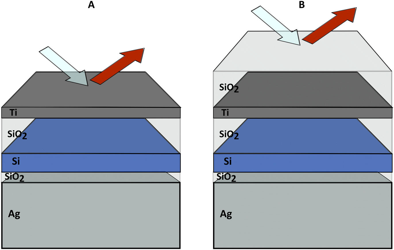 | ||
| Fig. 1 Schematic diagrams of the proposed asymmetric Fabry–Perot nanocavity designs: (A) Ag–SiO2–Si–SiO2–Ti, representing the MDSDM configuration, and (B) Ag–SiO2–Si–SiO2–Ti–SiO2, representing the MDSDMD configuration. | ||
Device fabrication employed a Denton Discovery-18 sputtering system. A 100 nm thick Ag film was sputtered onto microscope slides at 100 W DC power, under 5 mTorr argon pressure, with a deposition rate of 0.51 nm s−1. Subsequently, a 10 nm SiO2 spacer, a Si layer (5, 10, and 20 nm), an 80 nm SiO2 layer, and a 10 nm Ti top layer were sequentially deposited. For the AR-coated samples, an additional 80 nm SiO2 layer was deposited.
Throughout the process, venting between depositions was avoided to prevent oxidation of Ag and Si layers. Layer thicknesses were calibrated using a Wyko NT1100 interferometer. The deposition rates for SiO2, Si, and Ti were 0.02 nm s−1, 0.34 nm s−1, and 0.15 nm s−1, respectively. These configurations yielded six multilayer thin-film structures: three MDSDM and three MDSDMD samples.
Simulations and measurements
The optical properties of the MDSDM and MDSDMD structures were investigated using the transfer matrix method (TMM).42 This method modeled reflectance and absorptance across a wavelength range of 0.4–1.6 μm under normal and oblique incidence. Material refractive indices for the layers were obtained from established ref. 39–41 and 43 to ensure accurate representation of the optical response.Experimental reflectance spectra were measured using a halogen light source and two spectrometers: the Ocean Optics FLAME Miniature Spectrometer (0.2–0.830 μm) for the visible range and the Ocean Optics FLAME NIR Spectrometer (0.970–1.640 μm) for the NIR range. Normal incidence measurements employed a backscattering/normal reflectance probe provided by Ocean optics, and data were normalized to a thick Ag reference sample. Due to the wavelength ranges of the instruments, there is a spectral gap in measured data between 0.832 μm and 0.970 μm, which is accounted for in the numerical simulations to ensure continuity.
Structure modeling
The design and optimization of the proposed metal–dielectric–semiconductor–dielectric–metal (MDSDM) nanocavity and its anti-reflection (AR)-coated variant (MDSDMD) were guided by the transfer matrix method (TMM). This modeling approach allowed us to analyze the optical behavior of the cavity, particularly reflectance and absorptance, as functions of layer thicknesses and material properties. The modeling results formed the theoretical basis for achieving the desired narrowband reflection in the visible spectrum and broadband absorption in the near-infrared (NIR) range.Material selection and layer configuration
Silver (Ag) was used as the bottom reflective layer for its high reflectivity in the visible spectrum, while SiO2 acted as a lossless dielectric to enhance optical interference and increase light absorption in adjacent layers. Silicon (Si), with its relatively higher extinction coefficient (κ), contributes primarily through its optical loss profile. While no electronic or optoelectronic characteristics of Si are leveraged in this design, its optical loss properties enable enhanced absorptance in the NIR while preserving compactness. Comparable behaviour could be achieved with other lossy materials with similar n and κ values, though silicon's broad compatibility with sputtering and its tunability through thickness variations make it a strategic choice in this context. Titanium (Ti) served as the top reflective layer, introducing asymmetry to the Fabry–Perot nanocavity. The Ti layer's partial reflectivity and absorptive properties fine-tuned the spectral response, balancing performance and ease of deposition.Optimization of layer thicknesses
The optical response of the MDSDM structure was highly sensitive to the thicknesses of individual layers. Reflectance contour for varying Ti, Si, and SiO2 thicknesses are presented in Fig. 2. Variations in Ti thickness demonstrated minimal impact on the peak reflection wavelength but significantly influenced the bandwidth of the reflected spectrum. A thickness of 10 nm was chosen for Ti to ensure optimal partial reflectivity and ease of fabrication. The Si layer thickness had the greatest influence on the spectral response, with small variations (5–25 nm) resulting in substantial shifts in the peak reflection wavelength. This tunability underpins the structure's capability as a reflective color filter. While the top SiO2 layer primarily controlled the bandwidth of the reflected spectrum, the bottom SiO2 layer had a limited effect on spectral tuning. | ||
| Fig. 2 Contour plots of calculated reflectance spectra in the visible range showing the effect of varying: (A) Ti layer thickness, (B) Si spacer thickness, (C) top SiO2 thickness, and (D) bottom SiO2 thickness. | ||
Spectral performance analysis
The modeled reflectance spectra (Fig. 3) highlight the dual functionality of the MDSDM structure in the visible and near-infrared (NIR) ranges. In the visible spectrum, the structure exhibits narrowband reflection, with tunable peak wavelengths achieved by varying the silicon layer thickness (5–25 nm). This tunability makes the design well-suited for reflective color filter applications.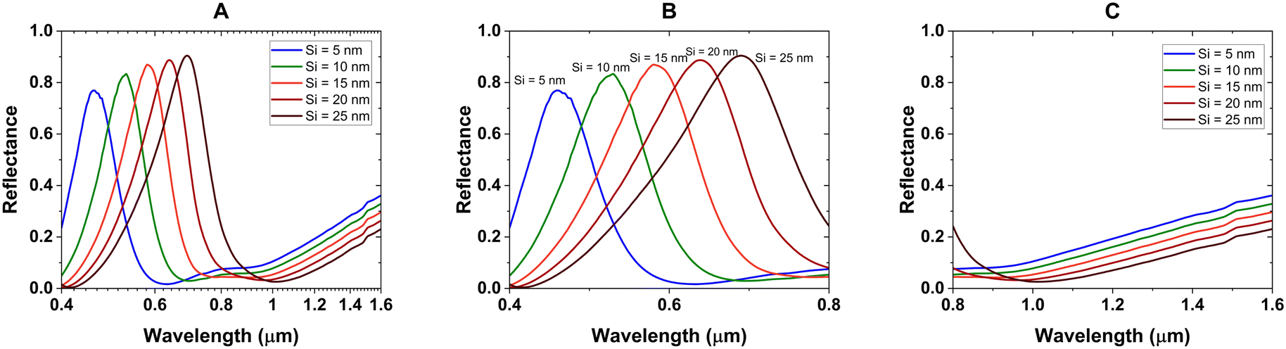 | ||
| Fig. 3 Normal-incidence reflectance spectra for the MDSDM structure: Ag (100 nm)–SiO2 (10 nm)–Si (5–25 nm)–SiO2 (80 nm)–Ti (10 nm). (A) Shows the full spectral range across the visible and NIR regions. (B) Provides an expanded view of the visible range, while (C) shows an expanded view of the NIR region, corresponding to the regions in (A). | ||
The TMM results presented in Fig. 3 cover 0.4–1.6 μm at a normal incidence angle. The evaluation shows selective color reflection for the visible range while demonstrating reflectance suppression below 30% across the 0.8–1.4 μm range. This behavior stems from the enhanced absorptive power of the silicon layer, which facilitates broadband absorption in the cavity.
The MDSDM structure also exhibits reduced sensitivity to variations in the angle of incidence. While Fig. 3 represents normal incidence behavior, additional modeling shows that the color reflectance remains stable under oblique angles for both S- and P-polarized light (Fig. 4). This angular robustness is explored further in the discussion of angular sensitivity.
 | ||
| Fig. 4 Angle-dependent reflectance spectra of the Ag (100 nm)–SiO2 (10 nm)–Si (5, 15, and 25 nm)–SiO2 (80 nm)–Ti (10 nm) structure. Panels (A, C and E) show S-polarized results, and (B, D and F) show P-polarized results for Si thicknesses of 5 nm, 15 nm, and 25 nm, respectively, at incident angles of 20°, 40°, and 60°. | ||
To further enhance AFPN's performance in the NIR range (0.8–1.6 μm), the addition of an anti-reflective (AR) coating helps increase the absorption to near unity while maintaining narrowband reflection in the visible spectrum (Fig. 5). These findings demonstrate the versatility of the proposed structure as both a reflective color filter and a broadband absorber.
 | ||
| Fig. 5 (A) Contour plot showing reflectance variation as a function of AR coating (SiO2) thickness for the structure: Ag (100 nm)–SiO2 (10 nm)–Si (15 nm)–SiO2 (80 nm)–Ti (10 nm)–AR layer. (B) Reflectance spectra in the visible and NIR ranges for the same structure with varying Si thicknesses (5–25 nm) and fixed AR coating thickness (80 nm). | ||
Results and discussion
Reflectance characteristics of the MDSDM structure
The proposed asymmetric Fabry–Pérot nanocavity (AFPN) structure, illustrated in Fig. 1, consists of SiO2–Si–SiO2 layers acting as spacers between Ag and Ti layers. A thick Ag base layer (100 nm) ensures high reflectivity and blocks light transmission, while the top Ti layer and the relatively lossy Si layer enable tunable spectral response.The fabricated devices, shown in Fig. 6(A), demonstrate distinct color reflection for varying Si layer thicknesses of 5 nm, 10 nm, and 20 nm, corresponding to blue, green, and orange films, respectively. The experimentally measured reflectance spectra for these samples (Fig. 6(B)–(D)) closely match the simulated results (Fig. 3), with a slight broadening of the full-width half maximum (FWHM) for the blue and orange films attributed to variations in the number density and damping factor of the sputtered Si layer.9,25
 | ||
| Fig. 6 (A) Optical image of fabricated MDSDM samples with Si thicknesses of 5 nm (blue), 10 nm (green), and 20 nm (orange). (B–D) Comparison of calculated and measured reflectance spectra for the same samples, corresponding to 5 nm, 10 nm, and 20 nm Si layers, respectively. | ||
This demonstrates the effectiveness of integrating a lossy material like Si within the cavity to achieve narrowband reflective color filters. Unlike traditional MIM-based Fabry–Pérot designs that absorb only a narrow frequency range and reflect the remainder,1,15,28 the proposed MDSDM structure achieves well-defined color reflection with minimal complexity, offering a scalable, lithography-free solution. While these results demonstrate effective spectral tuning for visible wavelengths, it is also critical to assess the device's performance under oblique light incidence, a key metric for real-world applications.
Angular sensitivity of reflectance
An essential performance metric for practical color filters is their angular response under oblique light incidence. Fig. 7 shows the angular dependence of reflectance for S- and P-polarized light at incident angles θ = 20°, 40°, and 60° for the fabricated samples.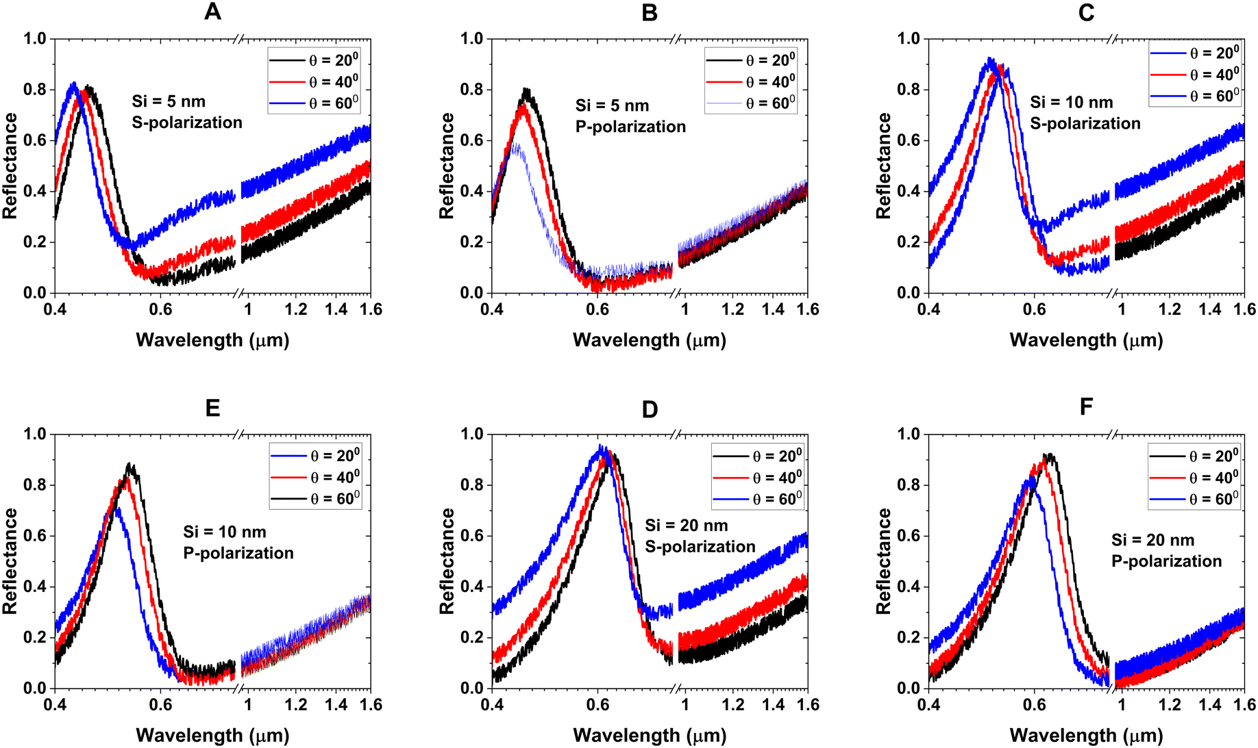 | ||
| Fig. 7 Measured reflectance spectra of the Ag (100 nm)–SiO2 (10 nm)–Si (5, 10, and 20 nm)–SiO2 (80 nm)–Ti (10 nm) structure under oblique incidence. Panels (A, C and D) show S-polarized light, and (B, E and F) show P-polarized light for Si thicknesses of 5 nm, 10 nm, and 20 nm, respectively, at angles of 20°, 40°, and 60°. | ||
For all samples, the reflectance spectra exhibit the expected blue shift with increasing incidence angles. This behavior arises from the lengthened optical path at oblique angles and variations in Fresnel reflection coefficients for S- and P-polarized light. Notably, the angular response remains predictable, with the spectral shift and intensity changes within acceptable limits for real-world applications.
The higher extinction coefficient of Si reduces interference-induced angular sensitivity, which is often observed in cavities with purely lossless SiO2 and TiO2 spacers.2,4 This angular robustness makes the MDSDM structure suitable for applications requiring stable color reflection under varying illumination conditions.
In addition to stable color reflection, the broadband absorption characteristics in the near-infrared region further highlight the versatility of the proposed MDSDM structure. A detailed comparison with prior studies is shown in Table 1, highlighting the advantages of silicon as part of the spacer materials.
Compared to Shurvinton's work, which achieves peak wavelengths of 0.425 μm (blue), 0.520 μm (green), and 0.7 μm (red) with SiO2 spacer thicknesses of 110 nm, 330 nm, and 215 nm respectively, the MDSDM structure achieves similar tunability with significantly lower spacer thickness variations (5 nm for blue, 10 nm for green, and 20 nm for orange). This results in a total cavity thickness of 95 nm (blue), 100 nm (green), and 110 nm (orange) in our design, with peak wavelengths of 0.470 μm, 0.522 μm, and 0.621 μm, respectively.
Similarly, Park et al. achieved resonance at multiple wavelengths using TiO2 spacers of varying thicknesses (65 nm for blue, 225 nm for green, and 135 nm for orange). However, the reliance on multiple resonances in their design results in multiple reflective peaks rather than a single defined wavelength reflection, reducing its spectral selectivity. In contrast, the MDSDM structure reflects a single, narrowband peak at the desired wavelengths, offering greater spectral precision and tunability.
This overall smaller thickness of the spacer makes the design less angle-sensitive, even at higher angles, keeping the reflection within the same color range. This means that for practical purposes, the reflected light will still appear blue, green, or orange, depending on the silicon layer thickness, without perceivable changes in color.
Beyond the spectral tuning range and angular response, other performance indicators, such as reflection efficiency, total number of layers, and ease of fabrication, are critical for practical deployment in multifunctional photonic systems. Table 2 presents a comparison of representative optical designs from recent literature, including both lithography-free and patterned structures such as colour filters and broadband absorbers. Compared to previous designs that require either nanostructuring or extensive tuning of dielectric thickness, the proposed MDSDM architecture offers a compact, lithography-free solution using five planar layers while achieving both visible color selectivity and broadband NIR absorption. The use of standard RF sputtering and avoidance of complex patterning techniques further highlight the manufacturability and scalability of this approach.
| Ref. | Optical response | Layer stack | Fabrication |
|---|---|---|---|
| Shurvinton et al.2 | High reflectance in RGB, no broadband NIR absorption | 3 layers | Lithography-free, sputtering |
| Park et al.4 | Multiple visible resonances, weak NIR selectivity | 3 layers | Lithography-free, sputtering |
| Osgouei et al.36 | Narrowband visible filtering, broadband NIR absorption | 5 layers | Nanostructure, hybrid stack |
| Lee et al.44 | Multiple visible resonances, no broadband NIR absorption | 5 layers | Lithography-free sputtering |
| This work | Narrowband RGB reflection, broadband NIR absorption, angle-insensitive | 5 layers | Lithography-free sputtering |
The optical robustness of the proposed design is further demonstrated in Fig. 7. For S-polarization, the intensity of reflectance in the visible spectrum remains stable with increasing angles, with a spectral blue shift of the peak wavelength observed due to the shorter effective optical path. Specifically, for the sample with a 5 nm silicon layer and a total cavity thickness of 95 nm, the peak wavelength shifts from 0.470 μm at normal incidence to 0.462 μm at 20°, 0.451 μm at 40°, and 0.440 μm at 60°. This stability in reflectance intensity can be attributed to the nature of S-polarized light, where the electric field vector is perpendicular to the plane of incidence. This polarization is less affected by angular variations because the Fresnel reflection coefficients for S-polarized light exhibit less dramatic changes at oblique angles, ensuring consistent reflectance intensity in the visible spectrum. However, in the NIR range, as the angle of incidence increases, the electric field component interacting with the silicon surface diminishes due to geometric projection effects. This reduction in the field's effective interaction with the silicon layer results in a decrease in NIR absorption.
In contrast, P-polarization, where the electric field vector lies in the plane of incidence, exhibits more angular sensitivity due to its stronger dependence on Fresnel coefficients at interfaces, particularly near the Brewster angle. This results in a visible drop in reflectance intensity and a spectral shift. For the 5 nm silicon sample, the peak wavelength shifts from 0.460 μm at 20° to 0.452 μm at 40° and 0.439 μm at 60°. The drop in intensity in the visible range is attributed to higher transmission and absorption losses at the interfaces for P-polarized light, which increase with angle. However, in the NIR range, the electric field has a component parallel to the plane of incidence enhancing the field interaction at the silicon interface, which helps maintain relatively consistent absorption across varying angles.
Enhanced NIR absorption with anti-reflection coating
To investigate the impact of the anti-reflection (AR) coating on the broadband absorption performance in the near-infrared (NIR) range, reflectance spectra were measured at normal incidence for the MDSDMD structures (Fig. 8). These structures are derived from the MDSDM cavities by incorporating an additional 80 nm SiO2 AR coating on the top layer (calculation for determining this thickness is presented in Fig. 5A). | ||
| Fig. 8 (A and C) Calculated and measured reflectance spectra in the NIR region for the AR-coated structure: Ag (100 nm)–SiO2 (10 nm)–Si (5, 10, and 20 nm)–SiO2 (80 nm)–Ti (10 nm)–SiO2 (80 nm). (B) Measured NIR reflectance spectra for the uncoated structure: Ag (100 nm)–SiO2 (10 nm)–Si (5, 10, and 20 nm)–SiO2 (80 nm)–Ti (10 nm). | ||
The measured reflectance spectra for the MDSDMD structures (Fig. 8A) demonstrate notable changes compared to the MDSDM configuration without the AR coating. Although a slight reduction in reflectance intensity is observed in the visible range, the AR coating substantially enhances absorption in the NIR region. The reflectance drops below 30% across the entire 0.8–1.6 μm range, with near-unity absorption achieved between 0.8–1.2 μm. This performance is a marked improvement over the MDSDM structure, where reflectance below 30% was maintained only up to 1.4 μm without the AR coating (Fig. 8B).
Fig. 8C highlights the enhanced NIR absorption capability of the MDSDMD structures, showcasing the reduced reflectance and near-unity absorption over an extended range. This enhancement arises from the AR coating's ability to suppress reflections at the air–dielectric boundary, thereby maximizing light interaction within the Fabry–Pérot cavity. The synergistic behavior of the AR coating and the spacer layers further optimizes the cavity's absorptive properties.
The experimental results confirm that the addition of the AR coating enhances the MDSDM structure's performance in the NIR range. This improvement underscores the potential of the MDSDMD structure for advanced applications such as improving the efficiency of NIR photodetectors, enhancing thermal imaging systems, and developing broadband absorbers for NIR-driven photovoltaics and sensors.
Conclusions
This study presents the optical response of an asymmetric Fabry–Pérot nanocavity (AFPN) featuring a series of dielectric–semiconductor–dielectric layers as a spacer medium. By incorporating a lossy semiconductor (silicon) within the cavity, the proposed metal–dielectric–semiconductor–dielectric–metal (MDSDM) AFPN structure addresses key challenges faced by conventional designs, such as low spectral shift sensitivity and high angular sensitivity. Numerical simulations using the transfer matrix method (TMM) identified optimal geometries for achieving enhanced performance across the visible and near-infrared (NIR) spectra.The fabricated planar structures exhibited dual functionality, demonstrating narrowband reflective color filtering in the visible range and significant broadband absorption in the NIR region. Experimental characterization revealed that the reflection peak could be precisely tuned by varying the silicon layer thickness by as little as 5 nm, enabling RGB color filtering with strong spectral selectivity. Additionally, the introduction of an anti-reflective (AR) coating further extended NIR absorption up to 1.6 μm without compromising visible range performance, achieving over 80% absorption between 0.8 μm and 1.5 μm.
In summary, this work demonstrates a scalable, lithography-free method for designing planar optical interfaces that combine narrowband visible reflection with broadband NIR absorption. The versatility of the proposed AFPN design, which enables tunable spectral response with sub 25 nm spacer thickness variation for red to blue color shift while maintaining broadband NIR absorption and reduced angular sensitivity, positions it as a cost-effective solution for applications in display technologies, optical sensing, thermal management, and photovoltaic systems. These findings contribute to the development of multifunctional nanoscale optical devices, offering practical solutions for applications involving surface and interface engineering.
Data availability
The datasets calculated, collected, and/or analyzed during the current study are available from the corresponding author upon reasonable request.Author contributions
K. P. D. conceived the research idea, conducted the investigation, and drafted the manuscript under the supervision of D. A. G.Conflicts of interest
The authors declare no conflict of interest.References
- M. A. Kats, R. Blanchard, P. Genevet and F. Capasso, Nanometre optical coatings based on strong interference effects in highly absorbing media, Nat. Mater., 2013, 12, 20–24 CrossRef CAS PubMed.
- R. Shurvinton, F. Lemarchand, A. Moreau and J. Lumeau, High-Chroma Color Coatings Based on Ag/SiO2/Ti/SiO2 Structures, Adv. Photonics Res., 2022, 3, 2200102 CrossRef CAS.
- A. Ghobadi, H. Hajian, M. C. Soydan, B. Butun and E. Ozbay, Lithography-free planar band-pass reflective color filter using a series connection of cavities, Sci. Rep., 2019, 9, 290 CrossRef PubMed.
- C.-S. Park and S.-S. Lee, Vivid coloration and broadband perfect absorption based on asymmetric Fabry–Pérot nanocavities incorporating platinum, ACS Appl. Nano Mater., 2021, 4, 4216–4225 CrossRef CAS.
- K. P. Dixit, Z. B. Houtman and D. A. Gregory, Reflective Color Filter Using Series Connection of Semiconductors in Asymmetric Fabry-Perot Nanocavity, IEEE Photonics Conference (IPC), 2023, pp. 1–2 Search PubMed.
- J. Guo, C. M. Huard, Y. Yang, Y. J. Shin, K.-T. Lee and L. J. Guo, ITO-free, compact, color liquid crystal devices using integrated structural color filters and graphene electrodes, Adv. Opt. Mater., 2014, 2, 435–441 CrossRef CAS.
- H. Liu, H. Yang, Y. Li, B. Song, Y. Wang, Z. Liu, L. Peng, H. Lim, J. Yoon and W. Wu, Switchable All-Dielectric Metasurfaces for Full-Color Reflective Display, Adv. Opt. Mater., 2019, 7, 1801639 CrossRef.
- J. Y. Lee, K.-T. Lee, S. Seo and L. J. Guo, Decorative power generating panels creating angle insensitive transmissive colors, Sci. Rep., 2014, 4, 4192 CrossRef PubMed.
- K. P. Dixit, Z. B. Houtman, E. E. James and D. A. Gregory, Electro-optical modulator using tunable III-V semiconductor in nanocavity, Physics and Simulation of Optoelectronic Devices XXXII, 2024, pp. 8–15 Search PubMed.
- S. Yokogawa, S. P. Burgos and H. A. Atwater, Plasmonic color filters for CMOS image sensor applications, Nano Lett., 2012, 12, 4349–4354 CrossRef CAS PubMed.
- R. R. Singh, D. Ho, A. Nilchi, G. Gulak, P. Yau and R. Genov, A CMOS/thin-film fluorescence contact imaging microsystem for DNA analysis, IEEE Trans. Circuits Syst. I: Regul. Pap., 2010, 57, 1029–1038 Search PubMed.
- M. Khorasaninejad, S. M. Raeis-Zadeh, H. Amarloo, N. Abedzadeh, S. Safavi-Naeini and S. S. Saini, Colorimetric sensors using nano-patch surface plasmon resonators, Nanotechnology, 2013, 24, 355501 CrossRef PubMed.
- L. Frey, P. Parrein, J. Raby, C. Pellé, D. Hérault, M. Marty and J. Michailos, Color filters including infrared cut-off integrated on CMOS image sensor, Opt. Express, 2011, 19, 13073–13080 CrossRef CAS PubMed.
- Z. Yong, S. Zhang, C. Gong and S. He, Narrow band perfect absorber for maximum localized magnetic and electric field enhancement and sensing applications, Sci. Rep., 2016, 6, 24063 CrossRef CAS PubMed.
- D. Wu, R. Li, Y. Liu, Z. Yu, L. Yu, L. Chen, C. Liu, R. Ma and H. Ye, Ultra-narrow band perfect absorber and its application as plasmonic sensor in the visible region, Nanoscale Res. Lett., 2017, 12, 1–11 CrossRef PubMed.
- H. J. Park, T. Xu, J. Y. Lee, A. Ledbetter and L. J. Guo, Photonic color filters integrated with organic solar cells for energy harvesting, ACS Nano, 2011, 5, 7055–7060 CrossRef CAS PubMed.
- Y.-H. Chen, C.-W. Chen, Z.-Y. Huang, W.-C. Lin, L.-Y. Lin, F. Lin, K.-T. Wong and H.-W. Lin, Microcavity-embedded, colour-tuneable, transparent organic solar cells, Adv. Mater., 2014, 26, 1129–1134 CrossRef CAS PubMed.
- H. Wang, Q. Chen, L. Wen, S. Song, X. Hu and G. Xu, Titanium-nitride-based integrated plasmonic absorber/emitter for solar thermophotovoltaic application, Photonics Res., 2015, 3, 329–334 CrossRef CAS.
- H. Wang and L. Wang, Perfect selective metamaterial solar absorbers, Opt. Express, 2013, 21, A1078–A1093 CrossRef PubMed.
- Y.-T. Yoon and S.-S. Lee, Transmission type color filter incorporating a silver film based etalon, Opt. Express, 2010, 18, 5344–5349 CrossRef CAS PubMed.
- K. P. Dixit, E. E. James and D. A. Gregory, Ultra-Broadband Visible to Near-Infrared Absorber Using Oxide-Coated Asymmetric Fabry-Perot Nanocavity, Laser Science, 2023, p. JTu4A–46 Search PubMed.
- Z. Li, E. Palacios, S. Butun, H. Kocer and K. Aydin, Omnidirectional, broadband light absorption using large-area, ultrathin lossy metallic film coatings, Sci. Rep., 2015, 5, 15137 CrossRef CAS PubMed.
- M. Chirumamilla, A. S. Roberts, F. Ding, D. Wang, P. K. Kristensen, S. I. Bozhevolnyi and K. Pedersen, Multilayer tungsten-alumina-based broadband light absorbers for high-temperature applications, Opt. Mater. Express, 2016, 6, 2704–2714 CrossRef CAS.
- Y. K. Zhong, S. M. Fu, N. P. Ju, M.-H. Tu, B.-R. Chen and A. Lin, Fully planarized perfect metamaterial absorbers with no photonic nanostructures, IEEE Photonics J., 2015, 8, 1–9 Search PubMed.
- K. P. Dixit and D. A. Gregory, Nanoscale modeling of dynamically tunable planar optical absorbers utilizing InAs and InSb in metal-oxide-semiconductor–metal configurations, Discover Nano, 2023, 18, 100 CrossRef CAS PubMed.
- C.-S. Park, V. R. Shrestha, S.-S. Lee, E.-S. Kim and D.-Y. Choi, Omnidirectional color filters capitalizing on a nano-resonator of Ag-TiO2-Ag integrated with a phase compensating dielectric overlay, Sci. Rep., 2015, 5, 8467 CrossRef CAS PubMed.
- K. P. Dixit, Design, Modeling, and Experimental Realization of Tunable Fabry-Perot Nanocavities for Broadband and Narrow-Band Applications, Ph.D. dissertation, The University of Alabama in Huntsville, 2024 Search PubMed.
- S. S. Mirshafieyan, T. S. Luk and J. Guo, Zeroth order Fabry-Perot resonance enabled ultra-thin perfect light absorber using percolation aluminum and silicon nanofilms, Opt. Mater. Express, 2016, 6, 1032–1042 CrossRef CAS.
- Z. Li, S. Butun and K. Aydin, Large-area, lithography-free super absorbers and color filters at visible frequencies using ultrathin metallic films, ACS Photonics, 2015, 2, 183–188 CrossRef CAS.
- K. P. Dixit, S. G. Weckerly and D. A. Gregory, Manipulating the Refractive Index of a Fabry-Perot Nanocavity Comprising Thin Semiconductor and Metal Films Using an External Electric Potential, 2023 Conference on Lasers and Electro-Optics (CLEO), 2023, pp. 1–2 Search PubMed.
- A. Ghobadi, H. Hajian, M. Gokbayrak, B. Butun and E. Ozbay, Bismuth-based metamaterials: from narrowband reflective color filter to extremely broadband near perfect absorber, Nanophotonics, 2019, 8, 823–832 CrossRef CAS.
- F. B. Barho, F. Gonzalez-Posada, M.-J. Milla, M. Bomers, L. Cerutti, E. Tournié and T. Taliercio, Highly doped semiconductor plasmonic nanoantenna arrays for polarization selective broadband surface-enhanced infrared absorption spectroscopy of vanillin, Nanophotonics, 2017, 7, 507–516 Search PubMed.
- M. Li, D. Liu, H. Cheng, L. Peng and M. Zu, Manipulating metals for adaptive thermal camouflage, Sci. Adv., 2020, 6, eaba3494 CrossRef CAS PubMed.
- L. Peng, D. Liu, H. Cheng, S. Zhou and M. Zu, A multilayer film based selective thermal emitter for infrared stealth technology, Adv. Opt. Mater., 2018, 6, 1801006 CrossRef.
- J. N. Anker, W. P. Hall, O. Lyandres, N. C. Shah, J. Zhao and R. P. Van Duyne, Biosensing with plasmonic nanosensors, Nat. Mater., 2008, 7, 442–453 CrossRef CAS PubMed.
- A. K. Osgouei, H. Hajian, A. E. Serebryannikov and E. Ozbay, Hybrid indium tin oxide-Au metamaterial as a multiband bi-functional light absorber in the visible and nearinfrared ranges, J. Phys. D: Appl. Phys., 2021, 54, 275102 CrossRef CAS.
- C. Ji, K.-T. Lee, T. Xu, J. Zhou, H. J. Park and L. J. Guo, Engineering light at the nanoscale: structural color filters and broadband perfect absorbers, Adv. Opt. Mater., 2017, 5, 1700368 CrossRef.
- Z. Chen, Z. Wen, Z. Wu, Y. Gao, C. Tan, Z. Deng, X. Li, D. Zhou, F. Liu and J. Hao, others Inverse-Designed Broadband Ultrathin Aperiodic Metacoatings Spanning from Deep Ultraviolet to Near Infrared, Laser Photonics Rev., 2025, 2301378 CrossRef CAS.
- D. T. Pierce and W. E. Spicer, Electronic structure of amorphous Si from photoemission and optical studies, Phys. Rev. B: Solid State, 1972, 5, 3017 CrossRef.
- K. J. Palm, J. B. Murray, T. C. Narayan and J. N. Munday, Dynamic optical properties of metal hydrides, ACS Photonics, 2018, 5, 4677–4686 CrossRef CAS.
- A. Ciesielski, L. Skowronski, M. Trzcinski and T. Szoplik, Controlling the optical parameters of self-assembled silver films with wetting layers and annealing, Appl. Surf. Sci., 2017, 421, 349–356 CrossRef CAS.
- P. Yeh, Optical Waves in Layered Media, Wiley, New Jersey, 2005, pp. 102–110 Search PubMed.
- L. Gao, F. Lemarchand and M. Lequime, Exploitation of multiple incidences spectrometric measurements for thin film reverse engineering, Opt. Express, 2012, 20, 15734–15751 CrossRef PubMed.
- J. Lee, J. Kim and M. Lee, High-purity reflective color filters based on thin film cavities embedded with an ultrathin Ge 2 Sb 2 Te 5 absorption layer, Nanoscale Adv., 2020, 2, 4930–4937 RSC.
| This journal is © The Royal Society of Chemistry 2025 |