
 Open Access Article
 This Open Access Article is licensed under a
 Creative Commons Attribution 3.0 Unported Licence
Effect of two-photon oxidation and calmodulin functionalization on the performance of graphene field-effect transistor biosensors†
Aku
Lampinen
 a,
Aleksei
Emelianov
a,
Erich
See
a,
Andreas
Johansson
ab and
Mika
Pettersson
*a
a,
Aleksei
Emelianov
a,
Erich
See
a,
Andreas
Johansson
ab and
Mika
Pettersson
*a
aNanoscience Center, Department of Chemistry, University of Jyväskylä, P.O. Box 35, FI-40014, Finland. E-mail: mika.j.pettersson@jyu.fi
bNanoscience Center, Department of Physics, University of Jyväskylä, P.O. Box 35, FI-40014, Finland
First published on 31st March 2025
Abstract
Solution-gated graphene field-effect transistors (GFETs) were fabricated for Ca2+ sensing. The GFETs were functionalized with two-photon oxidation (2PO) and calmodulin (CaM) immobilization, and the effects of these treatments and polymer residues on the sensor performance were systematically studied. Non-oxidized devices having polymer residues from lithographic processing showed initial LoDs of around 10−9 M and non-oxidized cleaner devices 10−8 M and the response of the devices was stable and reversible. 2PO showed a positive effect on the sensitivity of the devices, increasing the [Ca2+] dependent change in resistance at a constant gate voltage roughly by a factor of two, but at the cost of the LoD as 2PO increased the LoDs to up to 10−6 M. CaM functionalization was able to improve the LoD in some cases by two to three orders of magnitude, but its effect was limited most likely due to the intrinsic binding constants of the protein. However, CaM did not have a systematic effect on the magnitude of the response of the devices. Post-lithography polymer residues affected the LoD and response magnitude in a similar manner as 2PO, but also caused less reproducible behavior, indicating that a cleaner GFET surface is preferred for sensor applications.
Introduction
Intercellular communication, usually via chemical but also electrical signaling, enables the nervous system to perform complex processing.1 In chemical synapses, neurotransmitters (NTs) are released and diffused across the synaptic cleft to bind with postsynaptic receptors, transmitting signals between cells.1 At electrical synapses, the cells are directly connected via intercellular channels (i.e. gap junctions), where electrical current (e.g. Ca2+ ions) or small molecules are able to move through.2,3 Within neurons, the intracellular concentration of calcium ions ([Ca2+]) regulates many processes, with one of the most critical being the [Ca2+]-triggered release of NTs following an action potential.4 One promising method to detect this electrically triggered and chemically mediated signal, is to use a specific and sensitive biosensor.5 While sensors for measuring the electrical activity of neurons are available,6 there is an increasing demand for developing more specific sensors, capable of measuring NTs directly. Novel nanomaterials, in particular graphene, have high potential for bringing new solutions.7“The mother of all graphitic allotropes”,8 graphene is a two-dimensional hexagonal lattice of sp2-hybridized carbon atoms with extraordinary electronic (e.g. high conductivity), mechanical (e.g. flexibility and durability), and physical properties (e.g. high surface-to-volume ratio) which have sparked a plethora of research after the discovery of graphene.8,9 Even though the properties of graphene make it a very promising material for biosensing, pristine graphene is not selective towards analytes.10–13 Therefore, functionalization with receptor molecules is required to achieve selectivity.14–18 The functionalized graphene can then be used as the receptor and transducer layers of a biosensor.19 When working with solutions, a graphene field-effect transistor (GFET) configuration is one of the typical measurement geometries for graphene-based biosensors.20 It has been shown that by functionalizing GFETs fabricated from reduced graphene oxide (rGO) with calmodulin (CaM)—a protein that selectively binds to Ca2+ ions—it is possible to sensitize the devices to Ca2+.21 Without CaM, the devices were not sensitive to Ca2+.
Traditionally, to control the level of functionalization of graphene, working with graphitic flakes in a suspension21–27 and utilizing the modified Hummer's method28 to oxidize them to graphene oxide (GO) flakes is required. Then, covalent bonding can be used to attach biologically relevant molecules e.g. peptides26 to GO flakes. Further functionalization can be achieved by chemical,24,27,29 thermal,22,29 or UV irradiation29 processes, which can reduce the GO to rGO, increasing its conductivity. In contrast, single-layer graphene (SLG) functionalization has been controlled by e.g. exposure to low-energy hydrogen30 or oxygen plasma31 or addition of self-assembling monolayers.32,33 Most of these methods only work in bulk and lack spatial and functionalization level control.
Two-photon oxidation (2PO) is an optical method for functionalizing graphene with oxygen-containing groups via femtosecond-pulsed laser irradiation with high spatial and oxidation level control.34,35 By irradiating graphene with tightly focused ultrashort laser pulses in an ambient atmosphere, mainly epoxide and hydroxyl35 functional groups are introduced to the graphene lattice at low laser doses. The functional groups modify the electrical properties of graphene,34,36 its interactions with its surroundings,37–39 and change the hydrophobic graphene surface to an oxidized, more hydrophilic material. This can be utilized to control area-selective protein deposition on a chemical-vapor-deposition-grown (CVD) SLG surface, which in turn is useful for GFET functionalization.37,39
In this study, GFETs fabricated from CVD SLG, modified by 2PO and non-covalent protein functionalization were used to detect Ca2+ ions in deionized water (DI). Their response was compared to unmodified and non-functionalized devices. CaM was used to study its effect on the calcium concentration ([Ca2+]) dependent response of the microscale GFETs. The results show that 2PO had a positive effect on the [Ca2+] dependent response magnitude, the fabricated devices were durable, their behavior reversible, and they had their limit of detection (LoD) in the 3–30 nM range. Several GFETs functionalized with CaM demonstrated improved LoD of the GFETs, however, their response magnitude due to [Ca2+] change did not improve significantly.
Methods
The samples used were designed to fit into the male end of a high-definition multimedia interface (HDMI) cable, similar to our previous study.38 In brief, the samples were fabricated on a Si/SiO2 substrate and patterned by standard optical deep ultraviolet lithography using poly(methyl methacrylate) (950 PMMA A11 (Kayaku Advanced Materials)) as the photoresist. The evaporated metal patterns were 5 nm Ti + 90 nm Pd. The graphene was synthesized by chemical vapor deposition on a Cu surface and transferred to the Si/SiO2 substrate with a PMMA support layer,40 and reactive ion etching (O2 plasma, 30 W) was used to remove any excess graphene leaving 60 μm long and 15 μm wide graphene channels between the source and the drain. After removing the majority of the remaining PMMA with acetone, the graphene was first annealed in O2 (2 h, ∼300 °C) and then in Ar (∼400 sccm) + H2 (∼20 sccm) (2 h, ∼400 °C) to carbonize any possible PMMA polymer residues and remove the amorphous carbon before further processing. The final openings and passivation were done with PMMA that was patterned using electron beam lithography so that a 65 μm wide and 35 μm long window was formed on the graphene channel. Optical images of the sample and the device designs are shown in Fig. 1a)–c) with a cross-sectional schematic of the measurement geometry in Fig. 1d).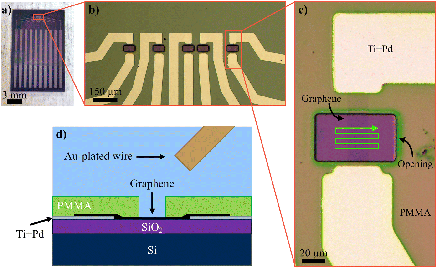 | ||
| Fig. 1 Optical images of a) a sample, b) all devices of one sample, and c) an individual device, where the 2PO irradiation pattern is illustrated with a bright green arrow and d) a cross-sectional schematic of the geometry of the solution-gated measurements, where the Ti + Pd leads were the source and drain and the Au-plated Ag wire worked as the gate electrode. | ||
After the samples were fabricated, they were heated on a hotplate (160 °C, 3 min) in order to strengthen the graphene–substrate interaction38,39 and the temperature was chosen so that no significant damage was caused to the passivation layer or graphene channel. The “hotplated” samples were then oxidized with 2PO.41 A 515 nm wavelength femtosecond (fs) pulsed laser (Pharos-10, Light Conversion Ltd., 600 kHz repetition rate, 250 fs pulse duration) was used to perform the oxidation. Every spot was irradiated for 1 s with a step size of ∼0.6 μm and spot size of 6 μm and the laser pulse energies were varied between 467–683 pJ.
After the oxidation, all devices were characterized by atomic force microscopy (AFM) using Dimension Icon with ScanAsyst (Bruker) and ScanAsyst Air probes (Bruker) and Raman spectroscopy using DXR Raman microscope (Thermo Scientific) with a 50× objective, 532 nm excitation wavelength, and 1 mW laser power. AFM was used to inspect the exposed graphene surface before and after protein incubation. Raman on the other hand was used to determine the intensity ratio between the D and G bands (ID/IG) to measure the achieved oxidation level35,42 as the irradiation dose does not always directly correlate with the oxidation level due to ambient conditions changing (humidity, room temperature etc.) and the presence of PMMA residues.38 Additionally, utilizing the methods described by Cançado et al.,43 the nature and density of defects were also analyzed by determining the average crystalline size (La) and the average distance between point-like defects (LD) from where the defect density (nD) was calculated.
The buffer solution used for the protein adsorption was a standard 1× PBS (phosphate-buffered saline) solution, prepared from PBS tablets (Fisher Scientific) and therefore had 10 mM PBS, 137 mM NaCl, and 2.7 mM KCl. The measurement solutions with [Ca2+] of 3 nM, 3 μM and 3 mM in DI (type 2 water from Elix Essential 3 UV water purification system, resistivity >15 MΩ cm with estimated total ionic concentration of <3 × 10⁻¹⁰ M) were diluted from a stock solution of 3 M, prepared by dissolving CaCl2 (anhydrous, purity >97%, Fluka) in DI. The protein used was a commercially available variant of calmodulin (CaM, bovine brain, high purity, Merck), which—after receiving the shipment—was aliquoted to 50 μL volumes of 500 μg mL−1 in 5× PBS (pH ≈ 7.4), flash frozen with liquid nitrogen, and stored at −70 °C until used.
Based on our previous work39 with this exact variant of CaM, the functionalization incubation conditions were selected to be pH ∼7 and [CaM] ≈ 2.5 μg mL−1. To attach the proteins to the graphene surface, a drop-casting incubation method was used,39 where first, a 10 mM PBS buffer solution with a protein concentration of 2.5 μg mL−1 was prepared. A 20 μL drop of the solution was pipetted on top of the graphene, and the chip was left in a humidity saturated container for 1 h to incubate. After the incubation, the chip was rinsed three times with 1 mL of the PBS buffer to remove excess protein and then 3 × 1 mL of deionized water to remove any residual salts. Immediately after the incubation, the sample was placed in the measurement setup, the active area immersed in DI to prevent the proteins from drying.
The electronic measurements were performed so that the tip of the HDMI chip with the GFETs was placed into a small container holding 3 ml of DI. The gate electrode was a ∼1 mm thick Ag wire with 250 nm thick Au coating evaporated (Baltec BAE 250, Balzers) on it. The different concentrations were achieved by pipetting 1, 10, or 100 μL of each measurement solution in increasing concentration order to the container with the sample. The resulting concentrations and their target concentrations are shown in Table S1 (ESI†). To make sure that the signal from the devices was stable and the increase in volume was not the source of the detected changes, the sample was subjected to a positive gate potential for an extended period of time (typically ∼1 h and +0.2 V) while the current through and the voltage across a device were constantly measured. When the measured values no longer drifted as a function of time, gate sweeps were performed before and after an addition of 100 μl of DI. When all of this showed the transfer curve being stable, the actual concentration dependency measurements were started. The details of the used in-house-built measurement setup have been described previously.38 Gate sweeps were performed by first scanning the gate voltage (UG) from 0 V to −0.3 V and from there the loops to +0.7 V and back to −0.3 V were measured with a constant scanning speed (∼0.1 V s−1). After the last loop, the potential was returned to 0 V. Each substrate and device went through two rounds of measurements without protein functionalization (Run 1 and Run 2) and then two rounds of measurements with protein functionalization (CaM 1 and CaM 2). This way the effect of protein on the exact individual devices was possible to determine.
The data from the electronic measurements was analyzed using a self-written Python script, which first corrected the measured drain-source current (IDS) by removing the measured drain-gate leakage current (IDG, typically two to three orders of magnitude lower than IDS), then calculated the drain-source resistance (RDS) from the measured drain-source voltage (UDS) and corrected current (IDS − IDG) and averaged ten loops into one. Although no significant hysteresis was detected, to simplify the data processing, out of the averaged scans for each condition, only the backwards (from +0.7 V to −0.3 V) parts were inspected to define the [Ca2+] response. To see the response of an individual device, the averaged loop was fit with a sum of Gaussian functions, where each Gaussian represented the behavior of a different peak or shoulder of the device response (component). The fact that there was more than one peak visible in the measurements reflects the heterogeneity of the transistor area with respect to functionalization, polymer residues, and other impurities. The number of Gaussians was defined by taking the numerical second derivative and using the number and locations of strong local minima (d2(RDS)/d(UG)2 ≪ 0). A fit of a single Gaussian function was used as a background correction for this component analysis. For LoD estimation, the allometric function y = A + BxC was fitted to the logarithmic concentration vs. response data (x vs. y), where A, B, and C were fit parameters. The response in this case is the normalized maximum resistance change (ΔRDS) at a constant UG value that has been extracted from all the transfer curves measured at different concentrations for each sample. Then the LoD was estimated to be the typical three times higher than the noise at the blank response level. As the response of the devices vs. [Ca2+] behaved exponentially, traditional definitions for sensitivity and LoD of the devices based on linear behavior were not possible to be used and instead the normalized maximal resistance change at the highest concentration (ΔRDS(10−4 M)) was used to reflect the sensitivity and a non-linear fitting method was used to define the LoD. See ESI† (supplementary note 1) for a more detailed description of the LoD estimation.
Results and discussion
The Raman characterization results of the GFET devices are shown in Fig. 2a), where the increase in oxidative functionalization could be seen clearly as an increase of the intensity of the D band (∼1350 cm−1) and as the formation of the D′ band (∼1625 cm−1), which was not visible in the non-irradiated devices. Defect analysis results based on the method proposed by Cançado et al.43 are shown in the ESI† (Table S2 and Fig. S2). All achieved oxidation levels stayed within the point-like defect regime i.e. the level of oxidation was relatively low. This led to p-type doping without drastic degradation of the electrical properties of the devices. The devices were named according to their substrate (S#) and device (d#) numbers (e.g. the first device on the second chip would be S2 d1). The Raman data and defect analysis results showed that between the two substrates used (S1 and S2) the initial state of the devices did vary a little, as the non-oxidized devices (S1 d1, S1 d2, S2 d3, and S2 d4) had their G bands at slightly different locations (1597–1598 cm−1 for S1 and ∼1595 cm−1 for S2). This could be explained with the AFM data (ESI,† Fig. S3), indicating that S1 devices did have slightly more PMMA residues than the S2 devices. Resist residues have been reported to affect graphene sensor performance.44 Also, the quality of the non-oxidized graphene was slightly different between the substrates as seen from the initial defect density (nD = 1.33–1.63 × 1011 cm−2 for S1 and 0.63–0.97 × 1011 cm−2 for S2) and intensity ratios of the D and G bands (ID/IG, 0.13–0.14 for S1 and 0.10–0.12 for S2). After the incubation and the electronic measurements, when the samples were dry, the graphene channels were imaged again to see the protein deposition. Examples of AFM scans of the surface of S1 d5 before and after protein functionalization are shown in Fig. 2b) and c), respectively.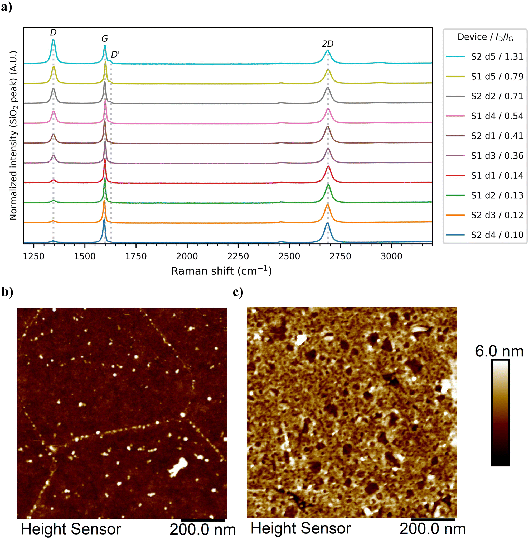 | ||
| Fig. 2 a) Averaged Raman spectra from device active area mapping for all the used devices, measured before any electrical measurements, in ascending oxidation level order with the main peaks named and indicated. The four lowest spectra are from non-oxidized, pristine devices (ID/IG = 0.10–0.14). The spectra have been normalized so that the maximum of the Si peak (not visible) has been set to the same value and then offset to stack them. Examples of the AFM topography images of the exposed graphene surface in the GFET channel of the oxidized S1 d5 b) before and c) after protein incubation. See ESI† for the measured AFM images of all the devices. | ||
After the initial characterization, the electronic measurements were performed so that four measurement runs were collected with each device of each substrate. The runs were named, in order, Run 1, Run 2, CaM 1, and CaM 2, where “Run #” refers to a measurement run without protein functionalization and “CaM #” refers to a measurement performed after the protein functionalization. To be specific, on each substrate, two of the devices were left with pristine graphene and the rest of them were oxidized with varying levels of oxidation. The performance of each device for sensing Ca2+ ions was measured twice before protein incubation, then the same devices were rinsed, protein immobilization incubation was performed, and measurements were performed again, twice. In this way, it was possible to reliably compare the performance of pristine, oxidized, and protein functionalized devices. In addition, the effect of the level of oxidation was determined accurately as the devices with different levels of oxidation were right next to each other on the same substrate. Such a study is enabled by the spatially selective 2PO process. The measured source-drain current (IDS) and potential (UDS) were used to calculate the resistance (RDS) of the graphene device as a function of the gate potential (UG). The calculated RDS transfer curve was then used for further analysis. For pristine device S1 d1, the whole measurement series consisting of four runs is shown in Fig. 3a)–d). For corresponding data on all the other devices, see Fig. S4 (ESI†).
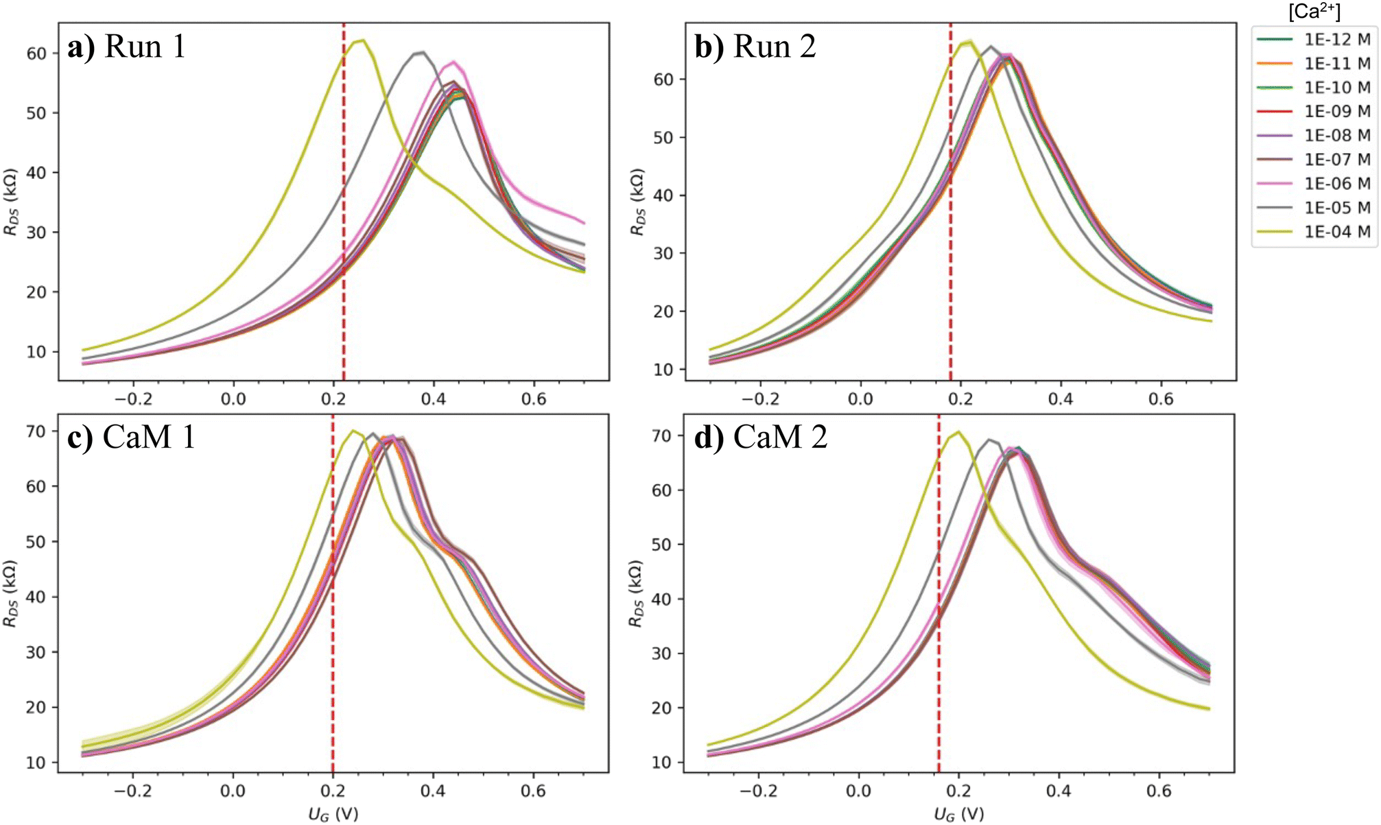 | ||
| Fig. 3 Examples of the RDS transfer curves of all the measurements done for a single pristine device (S1 d1). The measurements were performed in the following order: a) Run 1, b) Run 2, c) CaM 1, and d) CaM 2, where “Run #” and “CaM #” refer to a measurement without and with protein functionalization, respectively. The red vertical dashed lines indicate the UG at which the maximum ΔRDS was found for each measurement. See ESI† for full measurement data of all the devices. | ||
The first observation based on this data is that despite multiple processing steps and measurement runs, the behavior of the devices was stable as their resistance stayed in the same order of magnitude, functional, and fairly reversible. For some of the devices and measurements, there was more than one peak visible in the transfer curve, especially for the protein-functionalized devices. This could be explained by differently doped regions on the graphene channel due to pristine, residue-containing, and protein covered regions. The point of highest resistance, the charge neutrality point (CNP) location was also stable until micromolar [Ca2+] after which it moved strongly towards the zero-doping level. The reduced level of p-doping with increasing calcium ion concentration shows that the doping mechanism is complex and involves presumably dynamics of the solvation layer and negatively charged ions around the solvated ions and the positively doped graphene surface. However, this is a commonly observed phenomenon in GFET sensors.31,38,45,46 Theoretical simulations would be needed to understand the doping mechanism better. With the CaM functionalization, the initial doping changed differently depending on the substrate: For the more polymer residue contaminated S1, the initial doping increased (CNP is detected at a more positive UG) from Run 2 to CaM 1 and 2, and for the cleaner S2 the initial doping decreased. However, the CNP moved similarly as a function of [Ca2+] as before the functionalization. When inspecting a measurement series for each individual device, the common trend was that the resistance at the CNP (RCNP) increased as the different runs were performed. For S1 d1 in Run 1 (Fig. 3a)) RCNP was slightly over 60 kΩ, Run 2 (Fig. 3b)) over 65 kΩ, CaM 1 (Fig. 3c)) ∼70 kΩ, and in CaM 2 (Fig. 3d)) over 70 kΩ while the minimum resistance stayed the same. Therefore, as the measurements were performed, the transconductance (slope of the transfer curve) of the devices was improved.
The differences between Run 1 and Run 2 were most likely due to electrochemical cleaning of the device surface during the first measurement. This led to the change of doping at the beginning of the measurement run and therefore the measured transfer curve to significantly shift or show new peaks or shoulders. To see how all the different components behaved, Gaussian functions were fitted to every measurement. These different fitted components and the UDS locations at which the fitted component centers were detected are shown in the ESI† (Fig. S5) as an example for some concentrations of each run of two different devices. The normalized behavior of each component is shown in Fig. S6, (ESI†). The different components of the fits within the same run behaved similarly except for a couple of exceptions having a larger shift (Fig. S7, ESI†). The most significant exception was the second component of S1 d3 in Run 1, which appeared only at 10−5 M [Ca2+] and had a significantly larger shift than any other component of any other device in those conditions.
In Fig. 4 the [Ca2+] dependent transfer curves for four different devices on the same substrate (S2) are shown in ascending oxidation order. As the oxidation level was increased, the initial doping increased as the CNP moved from the 0.48–0.50 V range of the non-oxidized devices to 0.56 V for the device with the lowest level of oxidation, but then again decreased to 0.52 V for the two higher oxidation levels. For S1 the corresponding data is presented in the ESI† (Fig. S4).
 | ||
| Fig. 4 The RDS transfer curves for Run 1 of four different oxidation level devices on the same substrate with their ID/IG ratios shown. The red vertical dashed lines indicate the UG at which the maximum ΔRDS (i.e. the maximum response) was found for each measurement. See ESI† for full corresponding data of all the devices. | ||
As noted earlier, the transconductance varied between the devices, but irrespective of the oxidation level, the CNP moved quite similarly as a function of the [Ca2+]. Also, sweeping of the gate potential for locating the CNP is not an optimal way to run a GFET sensor continuously. A simpler and more practical way would be to set the gate potential to a certain value and measure variation in resistance. Therefore, to mimic this measurement setting and to better see the effect of the oxidation, the maximal change of resistance at a constant UG (ΔRDS) was extracted from the measured transfer curves and inspected for all the different 2PO levels.
The maximal ΔRDS for each run of each device is shown in Fig. 5a)–d). Looking at Run 1 (Fig. 5a)) a trend was seen that the higher the oxidation level, the higher the response magnitude. However, the trend does not seem to be completely monotonous as all S1 devices had a higher maximum ΔRDS than all the S2 devices despite some of them having lower oxidation levels.
 | ||
| Fig. 5 Normalized absolute maximum resistance change for each device in ascending oxidation level order (from black to green) for a) Run 1, b) Run 2, c) CaM 1, and d) CaM 2. The error bars indicate the variance of the averaged resistance. | ||
Another way to look at the data is to plot the ΔRDS between the lowest and highest concentration (ΔRDS(10−4 M)) reflecting the sensitivity for each device, as a function of the ID/IG ratio, which reflects the oxidation level (Run 1 in Fig. 6a)), for other runs see Fig. S8, ESI†). The plot reveals clearly that the oxidation increased the sensitivity. The sample-to-sample variation explains the difference in sensitivity for the S1 and S2 non-oxidized devices. However, when looking at the trends for each substrate individually, it was obvious that 2PO had a positive effect on the [Ca2+] sensitivity. In order to gain further insight into this, the ΔRDS(10−4 M) reflecting the sensitivity for each device was plotted against the G band location (Run 1 in Fig. 6b)), for other runs see Fig. S9, ESI†). The G band location is dependent on the doping, caused by various effects including 2PO and impurity-caused doping (e.g. PMMA residues). By plotting the sensitivity against the G band location, it is possible to qualitatively combine the effects of 2PO and doping by impurities. It indicated that the mechanisms that led to p-type doping enhanced the sensor performance by improving the transconductance. However, the [Ca2+] dependent movement of the CNP was not affected systematically. Even though the ΔRDS(10−4 M) increased as the oxidation level was increased, the LoD of the devices deteriorated as the oxidation level was increased (Fig. 6c)). One thing of note in Fig. 6c) is that the difference between the LoDs of very similarly treated devices varied significantly more within S1 than S2 (e.g. S1 d4 and S1 d5 vs. S2 d2 and S2 d5), which highlights the irreproducibility and unpredictability caused by the residual polymer contamination. For the LoDs estimated from the other measurement runs see Fig. S10† and for the effect of other sources of doping see Fig. S11 (ESI†).
 | ||
| Fig. 6 The difference in resistance between [Ca2+] = 10−12 M and 10−4 M depicting the sensitivity as a function of a) the ID/IG ratio and b) the Raman shift of the G band and c) the estimated LoD as a function of the ID/IG ratio for each device of both substrates in Run 1. See ESI† for corresponding plots for the other measurement runs. | ||
Regarding the effect of CaM functionalization of the GFETs, the results are summarized in Fig. 7. As the more PMMA-contaminated devices on S1 had a less reproducible behavior (significant deterioration of LoD between Run 1 and Run 2), their LoDs were systematically improved after Run 2 by one to two orders of magnitude by CaM. However, for all devices of S2—except S2 d2—the protein functionalization was not able to improve the LoD. This is surprising at first sight, as CaM is a calcium-binding protein. The reported47 intrinsic Ca2+ binding constant for CaM varies between 0.063 and 0.9 × 10⁻⁶ M for different binding sites and the actual dissociation constants detected vary between 0.2 and 20 × 10−6 M most likely depending on the ionic strength of the solution used.48 Our GFETs exhibited LoDs between 10−9 M and 10−5 M without protein functionalization and from 10−8 M to 10−6 M with CaM. Similar LoDs to our results have been achieved with CaM-functionalization of rGO (LoD ≈ 10−6 M)21 and boron-doped silicon nanowire (LoD ≤ 25 × 10−6 M)49 devices where they showed no sensitivity towards Ca2+ before CaM-functionalization. However, as our devices already showed [Ca2+] sensitivity at a similar and even lower concentration ranges, it is no wonder that an improvement in the LoD was not detected via CaM immobilization. This is why for S1 devices the CaM functionalization is able to improve the LoD after Run 2, as the initial LoD demonstrated by the devices in Run 1 deteriorated by two to three orders of magnitude. Another possible reason for the lack of LoD improvement for S2 devices is that the binding to cleaner graphene or oxidized graphene disturbed the calcium receptor site and hindered its natural function. There has been computational work regarding graphyne,50 which would indicate that all graphene-like materials could bind to CaM in a way that prevents its biofunctionality, which would mean that only the original ion sensitivity of the GFETs was detected in CaM 1 and 2. However, as CaM has been reported to induce binding and selectivity with rGO,21 this seems improbable. Additionally, the CaM could be already bound to Ca2+ before immobilization, but based on our previous work,39 the height of the immobilized CaM corresponds to its unbound conformation. In any case, the conclusion from this study is that the commercially available CaM improved the LoD of Ca2+ of most of the GFETs, but did not improve the magnitude of their response.
 | ||
| Fig. 7 LoDs for each device over all measurement runs showing the effect of the CaM functionalization. | ||
Conclusions
The effect of 2PO and CaM-functionalization on solution-gated GFETs was studied utilizing the excellent spatial control of 2PO. The behavior of the fabricated devices was stable with the maximum resistances staying within the same order of magnitude, reversible, and the devices were very durable as they survived several measurement runs pre and post protein functionalization. The devices showed shoulders or several peaks in their transfer curves due to having regions of pristine or 2PO-treated graphene with or without polymer residue or protein adsorption-related doping being present in the devices.The devices at different 2PO levels showed LoDs from 10−9 M to 10−5 M for [Ca2+] without protein functionalization and 10−8 M to 10−6 M with CaM functionalization. The 2PO treatment amplified the [Ca2+] dependent response of the devices but impaired the LoD. Also, both the sensitivity and LoD were affected by residual polymer and impurities on the device surface, which also resulted in lower reproducibility of the response. The immobilization of commercially available CaM showed a systematic improvement of LoD for most of the devices but had no significant effect on the magnitude of their response. For higher-sensitivity GFETs no improvement of the LoD was detected, indicating that the intrinsic Ca2+ binding constant of CaM was not low enough to improve the performance of the already-highly-sensitive GFETs.
Data availability
The data supporting this article have been included as part of the ESI.† The original files are available upon request from the corresponding author.Author contributions
A. L. lead the planning of the experiments in collaboration with the other authors, preformed the protein functionalization, AFM and Raman characterization, the electronic measurements, data analysis, and analysis related programming, and wrote the original manuscript. A. E. performed the 2PO and some of the Raman characterization and took part in the sample fabrication development. E. S. worked on the sample fabrication and fabrication development. A. J. and M. P. supervised the research. M. P. managed the project. A. L., A. E., E. S., A. J., and M. P. contributed to the discussion and manuscript editing.Conflicts of interest
There are no conflicts to declare.Acknowledgements
The authors acknowledge Olli Rissanen for the valuable technical work with sample and graphene fabrication and Emil Aaltonen foundation and Jane and Aatos Erkko foundation for funding this work.References
- S. E. Hyman, Curr. Biol., 2005, 15, R154–R158 CrossRef CAS PubMed.
- A. E. Pereda, Nat. Rev. Neurosci., 2014, 15, 250 CrossRef CAS PubMed.
- M. V. L. Bennett and R. S. Zukin, Neuron, 2004, 41, 495–511 CrossRef CAS PubMed.
- E. Neher and T. Sakaba, Neuron, 2008, 59, 861–872 CrossRef CAS PubMed.
- J. Ahlawat, M. Sharma and C. Shekhar Pundir, Microchem. J., 2023, 190, 108620 CrossRef CAS.
- Y. Nam and B. C. Wheeler, Crit. Rev. Biomed. Eng., 2011, 39, 45–61 CrossRef PubMed.
- W. Zhao, W. Zhang, J. Chen, H. Li, L. Han, X. Li, J. Wang, W. Song, C. Xu, X. Cai and L. Wang, ACS Sens., 2024, 9, 2705–2727 CrossRef CAS PubMed.
- A. K. Geim and K. S. Novoselov, Nat. Mater., 2007, 6, 183–191 CrossRef CAS PubMed.
- K. S. Novoselov, A. K. Geim, S. V. Morozov, D. Jiang, Y. Zhang, S. V. Dubonos, I. V. Grigorieva and A. A. Firsov, Science, 2004, 306, 666–669 CrossRef CAS PubMed.
- M. J. Allen, V. C. Tung and R. B. Kaner, Chem. Rev., 2010, 110, 132–145 CrossRef CAS PubMed.
- J. Kim, Q. Liu and T. Cui, Org. Electron., 2020, 78, 105551 CrossRef CAS.
- X. Tang, M. Debliquy, D. Lahem, Y. Yan and J.-P. Raskin, Sensors, 2021, 21, 1443 CrossRef CAS PubMed.
- Y. Lei, R. Zeng, Y.-T. Li, M.-M. Xiao, Z.-Y. Zhang and G.-J. Zhang, Carbon, 2023, 201, 616–623 CrossRef CAS.
- P. Suvarnaphaet and S. Pechprasarn, Sensors, 2017, 17, 2161 CrossRef PubMed.
- I. Fakih, O. Durnan, F. Mahvash, I. Napal, A. Centeno, A. Zurutuza, V. Yargeau and T. Szkopek, Nat. Commun., 2020, 11, 3226 CrossRef CAS PubMed.
- N. Alzate-Carvajal and A. Luican-Mayer, ACS Omega, 2020, 5, 21320–21329 CrossRef CAS PubMed.
- G. Xu, Z. A. Jarjes, V. Desprez, P. A. Kilmartin and J. Travas-Sejdic, Biosens. Bioelectron., 2018, 107, 184–191 CrossRef CAS PubMed.
- D. M. Goodwin, F. Walters, M. M. Ali, E. Daghigh Ahmadi and O. J. Guy, Chemosensors, 2021, 9, 174 CrossRef CAS.
- M. Pumera, Mater. Today, 2011, 14, 308–315 CrossRef CAS.
- L. J. A. Macedo, R. M. Iost, A. Hassan, K. Balasubramanian and F. N. Crespilho, ChemElectroChem, 2019, 6, 31–59 CrossRef CAS.
- H. G. Sudibya, Q. He, H. Zhang and P. Chen, ACS Nano, 2011, 5, 1990–1994 CrossRef CAS PubMed.
- S. C. Smith, F. Ahmed, K. M. Gutierrez and D. Frigi Rodrigues, Chem. Eng. J., 2014, 240, 147–154 CrossRef CAS.
- C. H. Lu, C. L. Zhu, J. Li, J. J. Liu, X. Chen and H. H. Yang, Chem. Commun., 2010, 46, 3116–3118 RSC.
- Y. Qi, W. Chen, F. Liu, J. Liu, T. Zhang and W. Chen, Environ. Sci.:Nano, 2019, 6, 1303–1309 RSC.
- H. Li, K. Fierens, Z. Zhang, N. Vanparijs, M. J. Schuijs, K. Van Steendam, N. Feiner Gracia, R. De Rycke, T. De Beer, A. De Beuckelaer, S. De Koker, D. Deforce, L. Albertazzi, J. Grooten, B. N. Lambrecht and B. G. De Geest, ACS Appl. Mater. Interfaces, 2016, 8, 1147–1155 CrossRef CAS PubMed.
- R. Chai, C. Xing, D. Gao, H. Yuan, Y. Zhan and S. Wang, Adv. Healthcare Mater., 2018, 7, 1800674 CrossRef PubMed.
- Q. He, H. G. Sudibya, Z. Yin, S. Wu, H. Li, F. Boey, W. Huang, P. Chen and H. Zhang, ACS Nano, 2010, 4, 3201–3208 CrossRef CAS PubMed.
- D. C. Marcano, D. V. Kosynkin, J. M. Berlin, A. Sinitskii, Z. Sun, A. Slesarev, L. B. Alemany, W. Lu and J. M. Tour, ACS Nano, 2010, 4, 4806–4814 CrossRef CAS PubMed.
- S. R. Shin, Y. C. Li, H. L. Jang, P. Khoshakhlagh, M. Akbari, A. Nasajpour, Y. S. Zhang, A. Tamayol and A. Khademhosseini, Adv. Drug Delivery Rev., 2016, 105, 255–274 CrossRef CAS PubMed.
- C. J. Russo and L. A. Passmore, Nat. Methods, 2014, 11, 649–652 CrossRef CAS PubMed.
- Q. Yuan, S. Wu, C. Ye, X. Liu, J. Gao, N. Cui, P. Guo, G. Lai, Q. Wei, M. Yang, W. Su, H. Li, N. Jiang, L. Fu, D. Dai, C.-T. Lin and K. W. A. Chee, Sens. Actuators, B, 2019, 285, 333–340 CrossRef CAS.
- T. Alava, J. A. Mann, C. Théodore, J. J. Benitez, W. R. Dichtel, J. M. Parpia and H. G. Craighead, Anal. Chem., 2013, 85, 2754–2759 CrossRef CAS PubMed.
- Y. Kamiya, K. Yamazaki and T. Ogino, J. Colloid Interface Sci., 2014, 431, 77–81 CrossRef CAS PubMed.
- J. Aumanen, A. Johansson, J. Koivistoinen, P. Myllyperkiö and M. Pettersson, Nanoscale, 2015, 7, 2851–2855 RSC.
- A. Johansson, H. C. Tsai, J. Aumanen, J. Koivistoinen, P. Myllyperkiö, Y. Z. Hung, M. C. Chuang, C. H. Chen, W. Y. Woon and M. Pettersson, Carbon, 2017, 115, 77–82 CrossRef CAS.
- A. V. Emelianov, D. Kireev, A. Offenhäusser, N. Otero, P. M. Romero and I. I. Bobrinetskiy, ACS Photonics, 2018, 5, 3107–3115 CrossRef CAS.
- E. D. Sitsanidis, J. Schirmer, A. Lampinen, K. K. Mentel, V. M. Hiltunen, V. Ruokolainen, A. Johansson, P. Myllyperkiö, M. Nissinen and M. Pettersson, Nanoscale Adv., 2021, 3, 2065–2074 RSC.
- A. Lampinen, E. See, A. Emelianov, P. Myllyperkiö, A. Johansson and M. Pettersson, Phys. Chem. Chem. Phys., 2023, 25, 10778–10784 RSC.
- A. Lampinen, J. Schirmer, A. Emelianov, A. Johansson and M. Pettersson, RSC Appl. Interfaces, 2024, 1, 1305–1316 RSC.
- V. M. Hiltunen, P. Koskinen, K. K. Mentel, J. Manninen, P. Myllyperkiö, M. Pettersson and A. Johansson, npj 2D Mater. Appl., 2021, 5, 1–7 CrossRef.
- K. K. Mentel, A. V. Emelianov, A. Philip, A. Johansson, M. Karppinen and M. Pettersson, Adv. Mater. Interfaces, 2022, 9, 2201110 CrossRef CAS.
- X. Díez-Betriu, S. Álvarez-García, C. Botas, P. Álvarez, J. Sánchez-Marcos, C. Prieto, R. Menéndez and A. De Andrés, J. Mater. Chem. C, 2013, 1, 6905–6912 RSC.
- L. G. Cançado, M. G. da Silva, E. H. M. Ferreira, F. Hof, K. Kampioti, K. Huang, A. Pénicaud, C. A. Achete, R. B. Capaz and A. Jorio, 2D Mater., 2017, 4, 025039 CrossRef.
- Y. Dan, Y. Lu, N. J. Kybert, Z. Luo and A. T. C. Johnson, Nano Lett., 2009, 9, 1472–1475 CrossRef CAS PubMed.
- M. Xue, C. Mackin, W.-H. Weng, J. Zhu, Y. Luo, S.-X. L. Luo, A.-Y. Lu, M. Hempel, E. McVay, J. Kong and T. Palacios, Nat. Commun., 2022, 13, 5064 CrossRef CAS PubMed.
- H. G. Oh, D. C. Jeon, M. S. Gianti, H. S. Cho, D. A. Jo, M. N. Indriatmoko, B. K. Jang, J. M. Lim, S. Cho and K. S. Song, Nanomaterials, 2021, 11, 787 CrossRef CAS PubMed.
- J. Haiech, C. B. Klee, J. G. Demaille and J. Haiech, Biochemistry, 1981, 20, 3890–3897 CrossRef CAS PubMed.
- C. B. Klee and T. C. Vanaman, in Advances in protein chemistry, ed. C. B. Anfinsen, J. T. Edsall and F. M. R. Richards, Academic Press, New York, 1982, vol. 35, pp. 213–303 Search PubMed.
- Y. Cui, Q. Wei, H. Park and C. M. Lieber, Science, 2001, 293, 1289–1292 CrossRef CAS PubMed.
- M. Feng, D. R. Bell, J. Luo and R. Zhou, Phys. Chem. Chem. Phys., 2017, 19, 10187–10195 RSC.
Footnote |
| † Electronic supplementary information (ESI) available. See DOI: https://doi.org/10.1039/d4lf00402g |
| This journal is © The Royal Society of Chemistry 2025 |