
 Open Access Article
 This Open Access Article is licensed under a Creative Commons Attribution-Non Commercial 3.0 Unported Licence
Physical properties of Fe-doped CdS quantum dots: single dot rectifying diode application
Piyali
Maity†
 a,
Ravi
Kumar
b,
S. N.
Jha
b,
D.
Bhattacharyya
b,
Sandip
Chatterjee
c,
Bhola Nath
Pal
d and
Anup Kumar
Ghosh
*a
a,
Ravi
Kumar
b,
S. N.
Jha
b,
D.
Bhattacharyya
b,
Sandip
Chatterjee
c,
Bhola Nath
Pal
d and
Anup Kumar
Ghosh
*a
aDepartment of Physics, Institute of Science, Banaras Hindu University, Varanasi, India. E-mail: akghosh@bhu.ac.in; Tel: +91 542 6701556
bAtomic & Molecular Physics Division, Bhabha Atomic Research Centre, Mumbai, India
cDepartment of Physics, Indian Institute of Technology (Banaras Hindu University), Varanasi, India
dSchool of Materials Science and Technology, Indian Institute of Technology (Banaras Hindu University), Varanasi, India
First published on 14th April 2025
Abstract
The domain of single-molecule based electronic devices has grown remarkably over the past decade by utilizing nanotechnology to improve the efficiency of device fabrication. However, most of the single-molecule devices are based on organic materials. Compared with organic molecules, quantum dots (QDs) are excellent owing to their crystalline nature, environmental stability, narrow emission band and quantum yield with tunable electronic and optoelectronic properties. Here, CdS:Fe QDs were synthesized and analyzed to assess their structural, optical, and electronic properties, and subsequently, they were implemented in fabricating single-dot rectifying diodes. EXAFS revealed the average coordination number of the doped Fe element. The ITO/TiO2/CdS:Fe quantum dot heterostructure rectifying diodes were grown by spin coating and were characterized using scanning tunneling microscopy (STM) at room temperature. STM images revealed the distribution of QDs over the substrate, and the spectra revealed the improved rectification behavior with tunneling up to ∼1000×, revealing their excellent diode functionality. Threshold voltage tuning from 1.62 eV to 0.83 eV indicated the application of these diodes for tunable electronics with low power consumption. Thus, these results indicate the promising use of CdS:Fe QDs for optimized ambient atmosphere rectifying diode applications, opening the way for innovative electronic devices with improved performance and functionality.
1. Introduction
Semiconductor technology is an essential part of modern life. Developments in microfabrication and optoelectronics are crucial for enabling advanced technologies in semiconductor industries. In recent decades, the use of electronic devices has massively expanded. This transformation has been made possible by the impressive developments in the fabrication and miniaturization of the active components of electronic devices. According to Moore's law, rapid miniaturization requires modern technologies.1 Miniaturization technologies focus on developing quantum-sized devices with little power consumption and low-cost market price. Single-molecule electronics have been explored for several decades as one of the possible routes for electronic devices. For example, single-molecule or single-dot devices with advanced functions such as molecular switches,2–4 single molecule diodes with high rectification,5–7 and single atom transistors8 have been fabricated. However, fabrication, reproducibility, and stability remain critical issues for single-molecule electronic devices. This could be resolved using single quantum dot semiconductor materials. CdS quantum dots (QDs) significantly compel electronic functions to make single-dot electronic devices.9–11 Quantum dots can enable the fabrication of highly efficient single-dot electronic devices. This work concentrates on the synthesis and characterization of self-assembled monolayer rectifying devices with a single QD or a small number of QDs.12–14The development of silicon-based electronic devices is becoming limited. Single-molecule electronic devices, which are getting more attention, are considered one of the most promising candidates to achieve the miniaturization of conventional electronic devices. Molecular-sized electronic devices must be miniaturized and integrated as much as possible to reduce power consumption. The performance of molecular electronic devices is based on the quantum confinement effect of electrons, which is different from traditional electronic devices. The semiconductor quantum dots based conventional electronic devices will gain enormous popularity.15–17 Therefore, our low threshold voltage rectifying diode is a possible solution. While remarkable advancements have been made in single-nanostructure devices and single organic molecule devices, there is a requirement for single quantum dot (QD)-based devices. This study aims to advance single nanoparticle or molecule nanoelectronics by reducing device size and enhancing performance. Colloidal quantum dots are promising materials due to their tunable physical properties, environmental stability, and advanced optoelectronic properties compared to organic molecules. This study aims to explore the single-dot electronic devices by rectifying diodes with high performance and low external power. Although there are many reports on CdS QDs and their applications, to the best of our knowledge, there is no report on Fe-doped CdS QDs thin film rectifying diodes. Various approaches to build and study the molecular junctions have been developed,18,19 including mechanically controllable break junctions (MCBJs),20,21 conductive atomic force microscopy electron migration scanning tunneling microscopy (STM) junctions,8,22–26 oxidative lithography27,28 or self-assembled methods,29 thermally evaporated and deposited metal film,30 and large-area molecular junctions.31 These techniques enable the probing of charge transport at the molecular and electronic levels.32–35 Because charge transport in single-dot junctions is quantum mechanical, molecular electronics offer unique opportunities for the discovery of fundamental physical phenomena and for the direct observation of effects that are not accessible in bulk materials. These effects include quantum interference (QI),36–38 the Coulomb blockade, and the Kondo effect. Moreover, devices with various remarkable functions such as single-molecule switches,4,39,40 molecular thermos-electronic devices,41,42 single-molecule diodes,43 single-molecule spintronic devices44,45 and sensors with single-molecule sensitivity46–49 have been explained within molecular junctions. An excellent imaging method for a broad range of possibilities for real space imaging on a scale that extends to atomic dimensions can be developed by STM and electrical property-related information can be obtained by this process.50,51
However, the implementation of techniques that are capable of atomic resolution, such as STM are needed to gain a profound dominance of the junction geometry in molecular-level experiments. Indeed, the possibility of incorporating an electrode within the STM geometry can favorably complement its high lateral resolution, giving an additional possibility of tuning the electronic properties of nanomaterial accessible by STM.52–57
This work discusses the tuned structural-, optical-, and electronic properties of iron (Fe) doped CdS quantum dots have been discussed. The synthesized quantum dots have been used to fabricate low threshold voltage thin film single dot rectifying diodes which will be useful as a switch or rectifier in day-to-day life. The importance of this study is the fabrication of single QD-based rectifying diodes that operate in ambient atmospheric conditions. Typically, single particle/molecule-based devices are studied by ultra-high vacuum STM studies. Meanwhile, this work demonstrates the operation of a device in open atmospheric conditions. In addition, the variable Fe-doping in CdS QDs helps to tune the threshold voltage, which plays an important role for practical applications. Moreover, this study used a simple fabrication technique (spin coating) and measurement techniques at ambient condition (STM) to fabricate and study single dot rectifying diodes. Iron (Fe) doping significantly enhanced the rectification behavior and reduced the threshold voltage, with potential development of advanced electronic systems with minimal electrical power loss.
2. Experimental details
For the synthesis of Fe-doped CdS quantum dots Cd1−xFexS (0 ≤ x ≤ 0.08), the precursors cadmium acetate di-hydrate, iron nitrate nano-hydrate, and sodium sulfide were used. The samples were prepared by the hot injection methods under an argon atmosphere at 100 °C for 12 h. Cadmium acetate di-hydrate and iron nitrate nano-hydrate were mixed in dimethyl sulfoxide solvent for 20 min. After that, a purged aqueous solution of sodium sulfide was added and mixed until the homogeneous solution was obtained. Then, 1-mono thioglycerol was added as a ligand. The solution was refluxed at 100 °C for 12 h. Then, the solution was cooled down to room temperature and washed with acetone and methanol. The yellow precipitate was collected and dried in vacuum.58 The synthesized quantum dots were characterized by X-ray diffraction (XRD), transmission electron microscopy (TEM), Raman spectroscopy, UV-vis spectroscopy, and photoluminescence spectroscopy (PL). The composition of Cd1−xFexS was calculated according to the stoichiometric ratio. Subsequently, the samples were prepared by adding the precursors stoichiometrically. The best fitted curve of Rietveld refinement of the XRD data confirm the composition of the materials. This also provides information on structural changes due to Fe incorporation. During the experiment, the doping process was precisely controlled to ensure uniformity and reproducibility of iron doping into the CdS. Multiple synthesis trials were performed, and the iron doping concentration was consistent across different batches.For the rectifying diode fabrication, the isopropanolic solution of TiO2 nanopowder (Sigma Aldrich) was coated on the cleaned surface of indium tin oxide (ITO) and heated at 350 °C for 30 min. Then, the single layer Fe-doped CdS quantum dots isopropanolic solution (1 mg/2 ml) was spin-coated at 1500 rpm. For characterization of the fabricated devices, scanning tunneling microscopy (STM) was performed in an ambient atmosphere. The devices were kept in vacuum until STM characterization.
The average crystallite sizes, D, of the samples are estimated from Debye–Scherrer's equation with X-ray diffraction data:
 | (1) |
The lattice parameter (a = b = c) was estimated from Rietveld refinement of the X-ray diffraction data and by using the following formula:
 | (2) |
The linear increase of the ‘a’ parameter can be explained based on the micro-strain developed due to Fe-doping. The micro-strain was calculated using the following equation:
 | (3) |
3. Results and discussion
3.1. X-ray diffraction (XRD) study
XRD measurements were performed for structural analysis of the prepared samples. The Rietveld refinement profiles of the prepared samples are shown in Fig. 1. Three prominent intense peaks at 2θ = 26.82°, 43.94°, and 51.86° corresponding to (111), (220), and (311) planes, respectively, confirm the cubic phase of CdS (JCPDS file #10-0454). All peak positions of undoped and Fe-doped CdS corresponding to the standard Bragg peaks of the zinc blende cubic structure are shown by the vertical bars, and the residue is represented by the line, respectively, at the bottom of the XRD patterns. The XRD patterns show that there is no appearance of any extra peaks or disappearance of any peak in the zinc blende structure of undoped CdS due to Fe doping. This confirms that the structure of the Fe-doped CdS in the zinc blende phase belongs to the F4![[3 with combining macron]](https://www.rsc.org/images/entities/char_0033_0304.gif) m space group. This analysis reveals that the samples are single-phased, having no trace of impurities. The well doped and crystalline structure was further confirmed by extended X-ray absorption fine structure spectroscopy (EXAFS). The close observation shows that the peak intensity for (111) peak decreases slightly with an increased doping concentration. The gradual decrement of the peak height with increasing Fe-concentration signifies the incorporation of Fe ions into the Cd-sites. The incorporation of Fe ions into the Cd-sites creates very small local distortion into the crystals (as observed from Raman spectra analysis) which causes a decrease in the peak height.58,59
m space group. This analysis reveals that the samples are single-phased, having no trace of impurities. The well doped and crystalline structure was further confirmed by extended X-ray absorption fine structure spectroscopy (EXAFS). The close observation shows that the peak intensity for (111) peak decreases slightly with an increased doping concentration. The gradual decrement of the peak height with increasing Fe-concentration signifies the incorporation of Fe ions into the Cd-sites. The incorporation of Fe ions into the Cd-sites creates very small local distortion into the crystals (as observed from Raman spectra analysis) which causes a decrease in the peak height.58,59
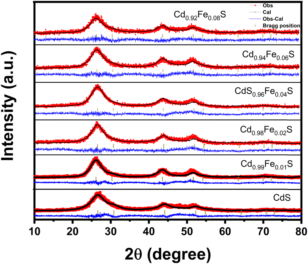 | ||
| Fig. 1 Rietveld refinement profiles of X-ray diffraction (XRD) data of undoped and Fe-doped CdS quantum dots [Cd1−xFexS, Fe = 0, 0.01, 0.02, 0.04, 0.06, and 008]. The experimental data are represented by ‘Obs’, and the theoretical fit by Rietveld refinement is represented by ‘Cal’. | ||
Variation of the average crystallite size with the Fe-doping concentration is depicted in Fig. 2a. The average crystallite size decreases linearly with the doping concentration. This result can be explained by the mechanism of growth kinetics. The chemical reactions follow two steps. In the first step, nucleation and interactions among the nucleation take place to reach the critical size. In the second step, these critical sizes grow into nanocrystals. The growth rate and the size can be explained based on the binding energy of the bonds.60
 | ||
| Fig. 2 (a) Average crystallite size variation, (b) variation in lattice parameter ‘a’, (c) variation in micro-strain, (d) variation in FWHM of peak (111) with varying Fe doping concentration in CdS QDs. The crystallite size is decreasing with increasing doping concentration owing to quantum confinement. | ||
The lattice parameters (a) have been estimated from Rietveld refinement and using eqn (2). The variation of ‘a’ with Fe-concentration (x) has been plotted in Fig. 2b, which shows that there is a small increase in the lattice parameter ‘a’ due to the increase of Fe-ion doping. A small increase in ‘a’ with Fe-doping cannot be attributed to the difference in ionic radii between divalent Fe (0.78 Å) and divalent Cd (0.96 Å) in tetrahedral coordination. It should be expected that the substitution of Cd2+ by Fe ions may lead to a decrease in the lattice parameters due to a smaller ionic radius of divalent Fe in tetrahedral coordination. Thus, the linear increase of the ‘a’ parameter cannot be explained by the difference in ionic radii. Moreover, linear variation of lattice constant ‘a’ with increasing Fe-concentration confirms that the Fe-ion has been substituted into the crystal lattice following Vegard's law. It also confirms that this is no structural change, and the doping of Fe-ions does not change the zinc blende structure of CdS. The variation of micro-strain with Fe concentration is plotted in Fig. 2c.
The XRD results reveal that the samples are cubic zinc blende in nature with broadening in the peaks due to their small size.58,59 The broadening increases with the doping concentration due to the decreasing size of the quantum dots with Fe doping concentration (Fig. 2d). This may be attributed to the quantum confinement effect, surface defect, and dopant induced strain;60,61 therefore, it is desirable to tune the efficiency of the single-dot-devices. The replacement of Cd with Fe during doping changes the lattice parameters and bond lengths of the CdS quantum dots, which results in the change in structural properties. The value of the average crystallite size, lattice constant (d), lattice parameter (a = b = c), and micro-strain are shown in Table 1.
| Sample | Position (2θ) | Average crystallite size (in nm) | d spacing (in Å) | Lattice parameter a (in Å) | Micro-strain |
|---|---|---|---|---|---|
| CdS | 26.887 | 2.278 | 3.312 | 5.736 | 0.87171 |
| Cd0.99Fe0.01S | 26.831 | 2.232 | 3.318 | 5.748 | 0.88976 |
| Cd0.98Fe0.02S | 26.822 | 2.123 | 3.319 | 5.750 | 0.93536 |
| Cd0.96Fe0.04S | 26.802 | 2.008 | 3.322 | 5.754 | 0.98884 |
| Cd0.96Fe0.06S | 27.155 | 2.007 | 3.329 | 5.766 | 0.98962 |
| Cd0.96Fe0.08S | 27.290 | 1.946 | 3.333 | 5.773 | 1.02066 |
3.2. Transmission electron microscopy (TEM)
A low-resolution transmission electron micrograph shows that the average grain size of the samples is 2 nm (Fig. 3a). The TEM result corroborates with the XRD measurement. Both the average crystallite size estimated from the XRD and the average grain size estimated from the TEM measurement are less than the Bohr radii of CdS (∼5.8 nm). From the low-resolution transmission electron micrograph, the monodispersive nature of the quantum dots has been observed, which is desirable in device fabrications. The irregular morphology in the TEM images can be attributed to the influence of the Fe doping. Fe is a transition metal and induces magnetism in the QDs after doping. The magnetism leads to jittering and distortion in the TEM images, which may affect the clarity of the morphology of the QDs. The selected area electron diffraction (SAED) pattern of 2% Fe-doped CdS quantum dots (Fig. 3b) reveals that the samples are polycrystalline in nature.58 The hkl values of planes are well matched with those of XRD measurements.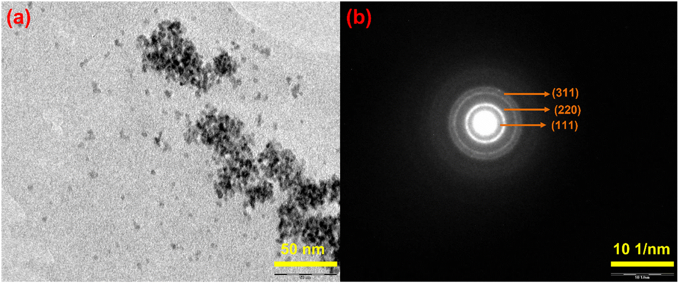 | ||
| Fig. 3 (a) Low resolution transmission electron microscopic image and (b) SAED pattern of 2% Fe-doped CdS quantum dots. | ||
3.3. EXAFS spectroscopy
The X-ray absorption fine structure spectroscopy (XAFS) analysis of iron (Fe) doped cadmium sulfide (CdS) quantum dots was carried out at the Energy Scanning EXAFS beamline (BL-9) within the energy range of 4 keV to 28 keV located at the Indus-2 Synchrotron source (2.5 GeV, 100 mA) on the cadmium (Cd) and iron (Fe) K-edges. The optical system includes a rhodium/platinum (Rh/Pt) coated collimating meridional cylindrical mirror, which reflects the collimated beam. This beam is then monochromatized using a silicon (Si) (111) double crystal monochromator (DCM) with a lattice spacing of 6.2709 Å. The second crystal of DCM is a sagittal cylinder utilized for horizontal beam focusing, while a downward-facing, Rh/Pt coated, bendable post mirror is employed for vertical beam focusing on the sample. To eliminate higher harmonic content in the X-ray beam, the second crystal of the DCM is detuned. X-ray absorption spectroscopy (XAS) measurements were carried out in both fluorescent and transmission modes.62,63EXAFS data analysis requires background subtraction and normalizing the results followed by theoretical EXAFS calculations based on one or more chosen structural models. The best match was obtained by comparing the calculated spectra with the actual data are and the parameters were refined. In the fluorescence mode, the sample is positioned at an angle of 45° to the incoming incident X-ray beam. A fluorescence detector is then strategically placed perpendicular to the direction of this incident beam to capture the emitted signals. To quantify the incident beam flux, an ionization chamber detector is situated before the sample. The fluorescence detector records the emitted fluorescence intensity. In the transmission measurement method, three ionization chambers (length of 300 mm) are employed for data collection. The first ionization chamber is used to measure the incident beam flux, the second one is used to gauge the transmitted beam flux, and the third chamber is used to record the X-ray absorption spectrum of a reference metal foil for the purpose of energy calibration. To optimize the signal-to-noise ratio (SNR), specific gas pressures and gas mixtures are selected.
 | ||
| Fig. 4 (a) Normalized XANES spectra, (b) normalized absorption spectra, (c) normalised EXAFS (k2χ(k) vs. k) spectra, and (d) Fourier-transformed EXAFS spectra of Cd0.99Fe0.01S and Cd0.96Fe0.04S quantum dots at the Cd K-edge. In (d), the black colored scatter points represent experimental spectra, and the red colored solid line represents the theoretical fit. | ||
Fig. 4c shows the k2χ(k) vs. k spectra while the χ(R) vs. R plots are shown in Fig. 4d for the Cd K-edge of the synthesized Fe-doped CdS quantum dots. The χ(R) vs. R data of these samples have been fitted by assuming the cubic structure of the CdS crystal. In the fitting process, the coordination number (C.N.), atom-to-atom bond distance (R), and the disorder factor (Debye–Waller factor) (σ2), which gives the mean square fluctuation in the atomic bond lengths and the thermal disorder in the system, have been used as fitting parameters and the best fit parameters are shown in Table 2. The contribution of the Cd–S coordination shell is confirmed by the presence of a peak at 2.0 Å in the radial distribution.64,65
| Path | Parameter | Cd0.99Fe0.01S | Cd0.96Fe0.04S |
|---|---|---|---|
| Cd K edge | |||
| Cd–S | R (Å) (2.52) | 2.49 ± 0.004 | 2.49 ± 0.002 |
| N(4) | 3.77 ± 0.1 | 3.59 ± 0.07 | |
 2
2
|
0.0057 ± 0.0006 | 0.0056 ± 0.0003 | |
| R factor | 0.009 | 0.003 | |
 | ||
| Fig. 5 (a) Normalized XANES spectra of Cd0.99Fe0.01S and Cd0.96Fe0.04S along with standard at the Fe K-edge, (b) normalized absorption spectra, (c) normalised EXAFS (k2χ(k) vs. k) spectra, and (d) Fourier-transformed EXAFS spectra of Cd0.99Fe0.01S and Cd0.96Fe0.04S quantum dots at the Fe K-edge. In (d), the black colored scatter points represent experimental spectra, and the red colored solid line represents the theoretical fit. | ||
| Path | Parameter | Cd0.99Fe0.01S | Cd0.96Fe0.04S |
|---|---|---|---|
| Fe K-edge | |||
| Fe–S1 | R (Å) (1.94) | 1.91 ± 0.002 | 1.90 ± 0.002 |
| N(3) | 3.0 ± 0.18 | 2.68 ± 0.08 | |
 2
2
|
0.0042 ± 0.0004 | 0.001 | |
| Fe–S2 | R (Å) (2.11) | 2.08 ± 0.002 | 2.07 ± 0.002 |
| N(3) | 3.0 ± 0.18 | 2.68 ± 0.08 | |
 2
2
|
0.0042 ± 0.0004 | 0.001 | |
| Fe–Fe | R (Å) (2.97) | 2.98 ± 0.003 | 3.01 ± 0.01 |
| N(4) | 4.0 ± 0.24 | 3.57 ± 0.1 | |
 2
2
|
0.0172 ± 0.0014 | 0.0097 ± 0.0004 | |
| R factor | 0.01 | 0.02 | |
3.4. Raman spectroscopy
Raman spectroscopy has been employed to investigate the local structure, vibrational modes and defect-oriented local disorders present in samples. An excitation of 532 nm using a laser has been used to record the Raman spectra at room temperature for undoped and Fe-doped CdS quantum dots in the spectral range of 200–1500 cm−1. CdS possesses the zinc blende cubic structure with space group F4m. Raman spectra of Cd1−xFexS QDs show that the prominent peaks relate to confined longitudinal optical (LO) phonon modes, and their overtones (2LO and 3LO) are clearly observed for undoped and Fe-doped CdS QDs (Fig. 6a). Three prominent peaks are located at 294, 588, and 885 cm−1 (Table 4), which correspond to the fundamental peaks related to stretching vibrations of LO phonon modes of 1LO, 2LO, and 3LO, respectively.58 For all optical modes, characteristic Raman peaks may be attributed to (i) the optical phonon confinement effect for the lower frequency mode66,67 and (ii) the surface optical (SO) phonons of spherical QDs,68 as evidenced by TEM. The magnified image of the 1LO peak of different Fe-doping shows that the peak position shifts towards higher values with increasing Fe concentration (Fig. 6b). This type of shifting can be explained on the basis of the Heisenberg uncertainty relation:| ΔpΔx ≥ ℏ2/4 | (4) |
| W(r) = exp[r2/2σ2] | (5) |
 | ||
| Fig. 6 (a) Raman spectra of Cd1−xFexS quantum dots at room temperature, (b) Raman spectra of Cd1−xFexS quantum dots: 1-LO (fitted to get the exact peak position), (c) FWHM variation (1-LO) with Fe doping concentrations, (d) relative Raman intensity of 1-LO with increasing Fe doping concentrations, (e) variation in exciton–phonon coupling strength with Fe doping concentration. | ||
| n = 1 | n = 2 | n = 3 | |
|---|---|---|---|
| CdS | 294 | 588 | 885 |
| CdS:Fe2 | 295 | 589 | 894 |
| CdS:Fe4 | 296 | 596 | 894 |
| CdS:Fe6 | 300 | 603 | 894 |
3.5. UV-vis spectroscopy and photoluminescence spectroscopy
Fig. 7a and b show the reflectance and absorbance spectra of direct band gap undoped and Fe-doped CdS quantum dots, respectively. Fig. 7c shows Tauc's plot for calculating the band gap. The band gaps have been calculated from the absorbance data using the Kubelka–Munk function.55 The inset of Fig. 7c shows the band gap variation of Fe-doped CdS. The reason behind the band gap variation is quantum confinement arising from the smaller size of QDs due to Fe doping which is consistent with average crystallite size variation. The obtained band gaps are 2.348 eV, 2.404 eV, 2.318 eV, 2.216 eV, and 2.022 eV for Fe doping at 0%, 1%, 2%, 4%, 6%, and 8%, respectively. The initial slight increase in the bandgap from 2.348 eV (Fe = 0%) to 2.404 eV (Fe = 1%) can be attributed to the Moss–Burstein effect, where the introduction of Fe3+ ions from Fe-precursor leads to an enhancement in carrier concentration. This enhancement in carrier concentration pushes the Fermi level towards the conduction band. This effectively helps widen the optical bandgap as a result of occupying the lower energy states in the conduction band. However, the bandgap begins to decrease with the further increase of Fe-concentration. This can be attributed to the creation of localized states within the bandgap, as a result of the interaction of Fe3+ ions with the host CdS. These localized states act as trap states which lead to band tailing and lowered bandgaps. | ||
| Fig. 7 (a) Reflectance spectra and (b) absorbance spectra of undoped and Fe-doped CdS quantum dots [Cd1−xFexS; Fe = 0%, 1%, 2%, 4%, 6%, and 8%]; (c) Tauc plots of undoped and Fe-doped CdS quantum dots (inset: band gap variation with Fe doping concentration). | ||
The photoluminescence spectra have been measured to determine the luminescence properties and defect states present in the samples. For this measurement, a fixed concentration of 1 mg sample/5 mL isopropanolic solution was maintained. The room-temperature photoluminescence spectra of undoped and Fe-doped CdS quantum dots (Fig. 8) indicate that the green luminescence peak near 530 nm increases with the doping concentration of Fe but suddenly falls in the 8% doped sample.58 This may be due to the precipitation of the samples with higher Fe concentrations in isopropanol solution. The band edge emission wavelengths near 480 nm are consistent with the UV-vis absorbance wavelength. Additionally, higher doping levels introduce structural disorder and induce defects. This result corroborates with the UV measurement contributing to the observed reduction in the bandgap at higher Fe-concentrations.
 | ||
| Fig. 8 Photoluminescence spectra of undoped and Fe-doped CdS [Cd1−xFexS] quantum dots. | ||
3.6. Rectifying diode behavior: scanning tunneling microscopy (STM) study
Scanning tunneling microscopy (STM) is a unique technique based on tunneling which yields surface topographies in real space and on an atomic scale. In this study, scanning tunneling spectroscopy (STS) has been used for investigation of rectification properties of single-dot diodes. Measurements using STM were carried out at room temperature. For practical application, it is essential to gain a high rectification ratio in single dot diodes and to modulate the performance of rectification. For single-molecule devices, the structure of the quantum dot has a significant impact on whether the molecular current exhibits rectification phenomenon. This idea will be addressed in other work. This study mainly focused on the mechanisms of rectification in single dot diodes and the efficient ways to modulate their rectifying performance.The schematic diagram of the device structure of the thin film single-dot rectifying diode has been displayed in Fig. 9a. Although, the schematic diagram is idealized using a very sharp tip in STM measurements, the ideal situation was nearly achieved. The current–voltage mechanism of device structure ITO/TiO2/CdS:Fe QDs has been measured by scanning tunneling microscopy at ambient atmosphere with a Pt/Ir tip. The TiO2 nano-powders were sonicated in isopropanol and spin-coated. Then, this thin film was annealed at 350 °C to obtain good crystallinity and phase formation. On the top of that layer, a single layer of Fe-doped CdS quantum dots was spin coated. Single dot devices with wide band gap TiO2 were fabricated for rectifying diodes due to their ambient atmosphere stability and transparent properties.
 | ||
| Fig. 9 (a) Device structure of the ITO/TiO2/Cd1−xFexS QDs rectifying diode [Fe = 0%, 2%, 4%, and 6%] and (b) rectifying behaviors of undoped and Fe-doped CdS single quantum dots (inset shows the scanning tunneling micrograph of 2% Fe-doped CdS QDs). (c) Schematic of the model of collective transport phenomena in the device. The yellow spheres denote CdS QDs. The dashed red line with arrows illustrates the electron transport path. | ||
The Pt/Ir tip for STM was used due to its high stability and conductivity in different types of measurements. Also, it has minimal reactivity with the material during imaging and spectral measurements. The Pt/Ir tip provides a stable and reliable interface between tip/material for high-resolution imaging and current–voltage measurements. However, the tip material can have an impact on the results in a contact-dependent device. The tip material could have indirect effects on the local electronic interaction between the tip and material, due to the work function of the tip. The work function of the tip can influence the contact barrier and the molecular states alignment with the Fermi level electrode.
The device has been characterized by an STM with an input current of 10 pA. The diode nature is observed from current–voltage plot (Fig. 9b) and the inset shows the image of the QDs surface. The tunneling current has been enhanced up to 10 nA, giving the rectification ratio 103. The threshold voltage decreases with doping concentration from 1.62 V (CdS) to 0.83 V (Cd0.94Fe0.06S) which makes it promising for low power consumption. In Fe-doped CdS QDs, the threshold voltage decreases due to the band gap decreasing with doping concentration. This may be attributed to the decrease of carrier concentration, which affects the energy band bending, resulting in an increase in depletion region width.74 At negative bias voltage to the substrate ITO, the holes transport through the valence band of CdS QD to TiO2 and TiO2 to ITO. This results in the high current in the STS data with turn-on voltage. For Fe-doped CdS QDs, holes transport through the additional Fe doping energy band (DB) near the valence band of CdS. As a result, the turn-on voltage gets lowered at higher doping concentration due to the broadening of this DB band. The negative tunneling current and negative substrate bias voltage indicates the hole tunneling. Moreover, the electron tunneling at positive substrate bias voltage is very negligible due to lack of electrons. The regions highlighted “1”, “2”, and “3” in Fig. 9b and TOC represent different positions of the 2% Fe-doped CdS QDs film.
The inset of Fig. 9b shows the image of dots of 2% Fe-doped CdS QDs. Slight vibration was experienced during the recording of images, which might be attributed to the magnetic behavior of Fe, which results in the unclear STM image of quantum dots.74
As electron tunnels from the STM tip to the QD, it will tunnel to another QD having far less polarization charge in order to reduce the Coulomb charging energy (Fig. 9c). Compared to the tip-to-dot and dot-to-substrate capacitances, the inter-dot capacitance is two orders of magnitude more significant to have a smaller Coulomb charging energy.75 The electron could tunnel to the nearest neighbor QD to reduce the high Coulomb charging energy in the CdS:Fe QD situated between the STM tip and the ITO substrate. As pointed out in the Middleton–Wingreen (MW) model, while Coulomb blockade can be observed when the series tunnel barriers are approximately equal, the Coulomb staircase requires asymmetric barriers so that multiple electrons or holes can be accumulated in the QD, with a low probability of tunneling out and a high probability of being replenished. A noticeable rectification of 103 was demonstrated using a Pt/Ir STM tip held at a constant position on the target dot. Fabricated devices showed consistent performance across multiple batches and with time, demonstrating their stability and repeatability. Although, the long-term stability or impact of environmental factors on QDs and rectifier diodes are important factors for the application in real-world single dot-based devices, the current study primarily focused on the initial performance and stability of the rectifying diodes under ambient atmospheric conditions (at normal temperature and pressure). The evaluation of the long-term stability and effects of environmental factors such as humidity and temperature fluctuations will be studied elsewhere.
4. Conclusions
We successfully characterized Fe-doped CdS quantum dots for application in inexpensive, solution-processed rectifying diodes using room-temperature scanning tunneling microscopy (STM). Cubic structures were confirmed using XRD and EXAFS. UV-vis spectra revealed the emergence of semiconductor behavior and a decrease in band gap upon Fe doping. Furthermore, conductance tunability of the CdS surface by individual dots was demonstrated. STM images showed that ITO/TiO2/CdS:Fe offered a rectification ratio of 103 in the rectifying diode. The maximum current was 10 nA owing to the instrument limitation. Tuning the threshold voltage from 1.66 eV to 0.83 eV (which is very low) indicated that the Fe-doped CdS quantum dots are promising for different electronic and optoelectronic applications with low electrical power loss. This study offers limited information on the potential application of QDs in rectifying diodes as the primary focus is on their STM analysis. STM results provided critical information regarding current–voltage characteristics for understanding the local electronic structure and surface morphology of QDs, which were crucial factors to understand and validate the behavior of the rectifying diode at the nanoscale level.This study contributes to understanding the fundamental properties of Fe-doped CdS quantum dots and offers a groundwork for their potential technological advancements in thin film rectifying diodes. The insights would provide a platform for further research aiming at utilizing the doped quantum dot-based rectifying diodes for improved device functioning and performance in many technological applications.
Data availability
The authors declare that all the data reported in this paper are available upon reasonable request.Conflicts of interest
There are no conflicts to declare.Acknowledgements
PM is thankful to DST, India for the INSPIRE Fellowship. AKG is thankful to DST-SERB, India (Grant no. CRG/2019/000896) and IoE (Scheme No.: 6031) for the financial support. AKG is thankful to DST-FIST; DST-PURSE; UGC-UPE programs for the financial support. Authors thank the Biophysics lab, Dept. of Physics (BHU) for providing the photoluminescence spectroscopy facility. Authors are also thankful to Prof. B. Ray for providing his lab for the synthesis of quantum dots.References
- M.-Y. Li, S.-K. Su, H.-S. P. Wong and L.-J. Li, Nature, 2019, 567, 169–170 CrossRef CAS PubMed.
- Z. Donhauser, B. Mantooth, K. Kelly, L. Bumm, J. Monnell, J. J. Stapleton, D. Price Jr, A. Rawlett, D. Allara and J. Tour, Science, 2001, 292, 2303–2307 CrossRef CAS PubMed.
- I. Franco, C. B. George, G. C. Solomon, G. C. Schatz and M. A. Ratner, J. Am. Chem. Soc., 2011, 133, 2242–2249 CrossRef CAS PubMed.
- J. L. Zhang, J. Q. Zhong, J. D. Lin, W. P. Hu, K. Wu, G. Q. Xu, A. T. Wee and W. Chen, Chem. Soc. Rev., 2015, 44, 2998–3022 RSC.
- I. Díez-Pérez, J. Hihath, Y. Lee, L. Yu, L. Adamska, M. A. Kozhushner, I. I. Oleynik and N. Tao, Nat. Chem., 2009, 1, 635–641 CrossRef PubMed.
- B. Capozzi, J. Xia, O. Adak, E. J. Dell, Z.-F. Liu, J. C. Taylor, J. B. Neaton, L. M. Campos and L. Venkataraman, Nat. Nanotechnol., 2015, 10, 522–527 CrossRef CAS PubMed.
- R. M. Metzger, Chem. Rev., 2015, 115, 5056–5115 CrossRef CAS PubMed.
- J. Park, A. N. Pasupathy, J. I. Goldsmith, C. Chang, Y. Yaish, J. R. Petta, M. Rinkoski, J. P. Sethna, H. D. Abruña and P. L. McEuen, Nature, 2002, 417, 722–725 CrossRef CAS PubMed.
- T. V. de Medeiros, A. Macina, J. P. de Mesquita and R. Naccache, RSC Appl. Interfaces, 2024, 1, 86–97 RSC.
- R. E. Castellanos-Pineda, A. Baron-Jaimes, M. A. Millán-Franco, M. E. Rincón and O. A. Jaramillo-Quintero, RSC Appl. Interfaces, 2024, 1, 741–747 RSC.
- L.-H. Lai, W.-H. Lin, C.-C. Hsieh and M. A. Loi, RSC Appl. Interfaces, 2024, 1, 122–132 RSC.
- L. Sun, Y. A. Diaz-Fernandez, T. A. Gschneidtner, F. Westerlund, S. Lara-Avila and K. Moth-Poulsen, Chem. Soc. Rev., 2014, 43, 7378–7411 RSC.
- F. Wu, H. Tian, Z. Yan, J. Ren, T. Hirtz, G. Gou, Y. Shen, Y. Yang and T.-L. Ren, ACS Appl. Mater. Interfaces, 2021, 13, 26161–26169 CrossRef CAS PubMed.
- A. Yakimov, V. Kirienko, A. Bloshkin, A. Dvurechenskii and D. Utkin, J. Phys. D: Appl. Phys., 2020, 53, 335105 CrossRef CAS.
- D. J. Frank, R. H. Dennard, E. Nowak, P. M. Solomon, Y. Taur and H.-S. P. Wong, Proc. IEEE, 2001, 89, 259–288 CrossRef CAS.
- G. Maruccio, R. Cingolani and R. Rinaldi, J. Mater. Chem. C, 2004, 14, 542–554 RSC.
- Y. Zhang, D. Tu, L. Wang, C. Li, Y. Liu and X. Chen, Mater. Chem. Front., 2024, 8, 192–209 RSC.
- D. Xiang, X. Wang, C. Jia, T. Lee and X. Guo, Chem. Rev., 2016, 116, 4318–4440 CrossRef CAS PubMed.
- T. Li, W. Hu and D. Zhu, Adv. Mater., 2010, 22, 286–300 CrossRef CAS PubMed.
- M. A. Reed, C. Zhou, C. Muller, T. Burgin and J. Tour, Science, 1997, 278, 252–254 CrossRef CAS.
- D. Xiang, H. Jeong, T. Lee and D. Mayer, Adv. Mater., 2013, 25, 4845–4867 CrossRef CAS PubMed.
- X. Cui, A. Primak, X. Zarate, J. Tomfohr, O. Sankey, A. Moore, T. Moore, D. Gust, G. Harris and S. Lindsay, Science, 2001, 294, 571–574 CrossRef CAS PubMed.
- S. Ho Choi, B. Kim and C. D. Frisbie, Science, 2008, 320, 1482–1486 CrossRef PubMed.
- W. Liang, M. P. Shores, M. Bockrath, J. R. Long and H. Park, Nature, 2002, 417, 725–729 CrossRef CAS PubMed.
- B. Xu and N. J. Tao, Science, 2003, 301, 1221–1223 CrossRef CAS PubMed.
- L. Venkataraman, J. E. Klare, C. Nuckolls, M. S. Hybertsen and M. L. Steigerwald, Nature, 2006, 442, 904–907 CrossRef CAS PubMed.
- X. Guo, J. P. Small, J. E. Klare, Y. Wang, M. S. Purewal, I. W. Tam, B. H. Hong, R. Caldwell, L. Huang and S. O'brien, Science, 2006, 311, 356–359 CrossRef CAS PubMed.
- Y. Cao, S. Dong, S. Liu, L. He, L. Gan, X. Yu, M. L. Steigerwald, X. Wu, Z. Liu and X. Guo, Angew. Chem., 2012, 124, 12394–12398 CrossRef.
- J. Tang, Y. Wang, J. E. Klare, G. S. Tulevski, S. J. Wind and C. Nuckolls, Angew. Chem., 2007, 119, 3966–3969 CrossRef.
- S. Kubatkin, A. Danilov, M. Hjort, J. Cornil, J.-L. Bredas, N. Stuhr-Hansen, P. Hedegård and T. Bjørnholm, Nature, 2003, 425, 698–701 CrossRef CAS PubMed.
- H. B. Akkerman, P. W. Blom, D. M. De Leeuw and B. De Boer, Nature, 2006, 441, 69–72 CrossRef CAS PubMed.
- N. J. Tao, Nat. Nanotechnol., 2006, 1, 173–181 CrossRef CAS PubMed.
- S. V. Aradhya and L. Venkataraman, Nat. Nanotechnol., 2013, 8, 399–410 CrossRef CAS PubMed.
- K. Moth-Poulsen and T. Bjørnholm, Nat. Nanotechnol., 2009, 4, 551–556 CrossRef CAS PubMed.
- S. M. Lindsay and M. A. Ratner, Adv. Mater., 2007, 19, 23–31 CrossRef CAS.
- C. Lambert, Chem. Soc. Rev., 2015, 44, 875–888 RSC.
- C. M. Guédon, H. Valkenier, T. Markussen, K. S. Thygesen, J. C. Hummelen and S. J. Van Der Molen, Nat. Nanotechnol., 2012, 7, 305–309 CrossRef PubMed.
- S. Ballmann, R. Härtle, P. B. Coto, M. Elbing, M. Mayor, M. R. Bryce, M. Thoss and H. B. Weber, Phys. Rev. Lett., 2012, 109, 056801 CrossRef PubMed.
- C. Jia, A. Migliore, N. Xin, S. Huang, J. Wang, Q. Yang, S. Wang, H. Chen, D. Wang and B. Feng, Science, 2016, 352, 1443–1445 CrossRef CAS PubMed.
- Z. Liu, S. Ren and X. Guo, Molecular-Scale Electronics: Current Status and Perspectives, 2017, pp. 173–205 Search PubMed.
- P. Reddy, S.-Y. Jang, R. A. Segalman and A. Majumdar, Science, 2007, 315, 1568–1571 CrossRef CAS PubMed.
- D. Nozaki, S. M. Avdoshenko, H. Sevincli and G. Cuniberti, J. Appl. Phys., 2014, 116, 074308 CrossRef.
- M. Elbing, R. Ochs, M. Koentopp, M. Fischer, C. von Hänisch, F. Weigend, F. Evers, H. B. Weber and M. Mayor, Proc. Natl. Acad. Sci. U. S. A., 2005, 102, 8815–8820 CrossRef CAS PubMed.
- W. Y. Kim and K. S. Kim, Acc. Chem. Res., 2010, 43, 111–120 CrossRef CAS PubMed.
- S. Sanvito, Chem. Soc. Rev., 2011, 40, 3336–3355 RSC.
- X. Guo, Adv. Mater., 2013, 25, 3397–3408 CrossRef CAS PubMed.
- Y. Zhao, B. Ashcroft, P. Zhang, H. Liu, S. Sen, W. Song, J. Im, B. Gyarfas, S. Manna and S. Biswas, Nat. Nanotechnol., 2014, 9, 466–473 CrossRef CAS PubMed.
- J. Wang, F. Shen, Z. Wang, G. He, J. Qin, N. Cheng, M. Yao, L. Li and X. Guo, Angew. Chem., 2014, 126, 5138–5143 CrossRef.
- G. He, J. Li, H. Ci, C. Qi and X. Guo, Angew. Chem., 2016, 128, 9182–9186 CrossRef.
- M. Hawley, I. D. Raistrick, J. G. Beery and R. J. Houlton, Science, 1991, 251, 1587–1589 CrossRef CAS PubMed.
- P. Vancsó, G. Z. Magda, J. Pető, J.-Y. Noh, Y.-S. Kim, C. Hwang, L. P. Biró and L. Tapasztó, Sci. Rep., 2016, 6, 29726 CrossRef PubMed.
- A. Aviram, C. Joachim and M. Pomerantz, Chem. Phys. Lett., 1988, 146, 490–495 CrossRef CAS.
- C. Joachim, J. K. Gimzewski, R. R. Schlittler and C. Chavy, Phys. Rev. Lett., 1995, 74, 2102 CrossRef CAS PubMed.
- A. Zhao, Q. Li, L. Chen, H. Xiang, W. Wang, S. Pan, B. Wang, X. Xiao, J. Yang and J. Hou, Science, 2005, 309, 1542–1544 CrossRef CAS PubMed.
- T. Komeda, H. Isshiki, J. Liu, Y.-F. Zhang, N. Lorente, K. Katoh, B. K. Breedlove and M. Yamashita, Nat. Commun., 2011, 2, 217 CrossRef PubMed.
- S. Schmaus, A. Bagrets, Y. Nahas, T. K. Yamada, A. Bork, M. Bowen, E. Beaurepaire, F. Evers and W. Wulfhekel, Nat. Nanotechnol., 2011, 6, 185–189 CrossRef CAS PubMed.
- S. Kahle, Z. Deng, N. Malinowski, C. Tonnoir, A. Forment-Aliaga, N. Thontasen, G. Rinke, D. Le, V. Turkowski and T. S. Rahman, Nano Lett., 2012, 12, 518–521 CrossRef CAS PubMed.
- P. Maity, S. Kumar, R. Kumar, S. Jha, D. Bhattacharyya, S. Barman, S. Chatterjee, B. N. Pal and A. K. Ghosh, J. Phys. Chem. C, 2021, 125, 2074–2088 CrossRef CAS.
- P. Maity, S. V. Singh, S. Biring, B. N. Pal and A. K. Ghosh, J. Mater. Chem. C, 2019, 7, 7725–7733 RSC.
- B. Prajapati, S. Kumar, M. Kumar, S. Chatterjee and A. K. Ghosh, J. Mater. Chem. C, 2017, 5, 4257–4267 RSC.
- J. Hwang, M. Pototschnig, R. Lettow, G. Zumofen, A. Renn, S. Götzinger and V. Sandoghdar, Nature, 2009, 460, 76–80 CrossRef CAS PubMed.
- K. Boldt, S. Bartlett, N. Kirkwood and B. Johannessen, Nano Lett., 2020, 20, 1009–1017 CrossRef CAS PubMed.
- L. Haddad, D. Gianolio, D. J. Dunstan, Y. Liu, C. Rankine and A. Sapelkin, Nanoscale, 2024, 16, 5768–5775 RSC.
- K. A. Svit, A. A. Zarubanov, T. A. Duda, S. V. Trubina, V. V. Zvereva, E. V. Fedosenko and K. S. Zhuravlev, Langmuir, 2021, 37, 5651–5658 CrossRef CAS PubMed.
- Y. Zhang, H. Zhang, D. Chen, C.-J. Sun, Y. Ren, J. Jiang, L. Wang, Z. Li and X. Peng, Nano Lett., 2021, 21, 5201–5208 CrossRef CAS PubMed.
- H. Richter, Z. Wang and L. Ley, Solid State Commun., 1981, 39, 625–629 CrossRef CAS.
- I. Campbell and P. M. Fauchet, Solid State Commun., 1986, 58, 739–741 CrossRef CAS.
- F. Comas and C. Trallero-Giner, Phys. Rev. B: Condens. Matter Mater. Phys., 2003, 67, 115301 CrossRef.
- A. Singha, B. Satpati, P. Satyam and A. Roy, J. Phys.: Condens. Matter, 2005, 17, 5697 CrossRef CAS PubMed.
- A. K. Arora, M. Rajalakshmi, T. Ravindran and V. Sivasubramanian, J. Raman Spectrosc., 2007, 38, 604–617 CrossRef CAS.
- K. Roodenko, I. Goldthorpe, P. McIntyre and Y. Chabal, Phys. Rev. B: Condens. Matter Mater. Phys., 2010, 82, 115210 CrossRef.
- P. Maity, R. Kumar, S. Jha, D. Bhattacharyya, R. K. Singh, S. Chatterjee and A. K. Ghosh, J. Mater. Sci.: Mater. Electron., 2022, 33, 21822–21837 CrossRef CAS.
- A. Rolo and M. Vasilevskiy, J. Raman Spectrosc., 2007, 38, 618–633 CrossRef CAS.
- M. El-Hagary and S. Soltan, J. Appl. Phys., 2012, 112, 043907 CrossRef.
- B. Paquelet Wuetz, D. Degli Esposti, A.-M. J. Zwerver, S. V. Amitonov, M. Botifoll, J. Arbiol, A. Sammak, L. M. Vandersypen, M. Russ and G. Scappucci, Nat. Commun., 2023, 14, 1385 CrossRef CAS PubMed.
Footnote |
| † Present address: City University of New York, 695 Park Ave, New York, NY 10065, USA. |
| This journal is © The Royal Society of Chemistry 2025 |