
 Open Access Article
 This Open Access Article is licensed under a Creative Commons Attribution-Non Commercial 3.0 Unported Licence
Label-free differentiation of living versus dead single yeast cells using broadband electrical impedance spectroscopy†
Amirhossein
Favakeh
 a,
Amir
Mokhtare
a,
Mohammad Javad
Asadi
b,
James C. M.
Hwang
bc and
Alireza
Abbaspourrad
*a
a,
Amir
Mokhtare
a,
Mohammad Javad
Asadi
b,
James C. M.
Hwang
bc and
Alireza
Abbaspourrad
*a
aFood Science Department, College of Agriculture and Life Sciences (CALS), Cornell University, Ithaca 14853, New York, USA. E-mail: alireza@cornell.edu
bSchool of Electrical and Computer Engineering, Cornell University, Ithaca, New York 14853, USA
cDepartment of Materials Science and Engineering, Cornell University, Ithaca, New York 14853, USA
First published on 24th February 2025
Abstract
The use of the intrinsic electrical properties of a single cell by broadband electrical impedance spectroscopy (EIS) as a label-free and non-invasive method to monitor cellular and intracellular features is an emerging field. Here, we present a novel EIS-based sheathless microfluidic platform with an integrated coplanar waveguide to probe the interior of a single cell. This platform allows for precise single-cell trapping by dielectrophoresis, hydrodynamic focusing, and sensing the electrical properties of the trapped single cell. We measured the impedance characteristics of a single Schizosaccharomyces pombe (fission) yeast cell by a single frequency sweep (30 kHz to 6GHz) in a stagnant sucrose solution using two-port scattering (S) parameters. The measurements revealed a clear distinction between the cytoplasm impedance of live versus dead cells at 3 GHz. This platform could provide real-time monitoring of cellular electrical responses to chemical and physical antagonists for diagnostic purposes.
Introduction
Single-cell biophysical characterization has gained considerable attention among biologists who seek to understand the mechanisms and processes that take place within this small unit of life.1 Biophysical characterization of a single cell provides a wealth of information, including viability,2 morphology,3 mechanical properties,4 and physiological state,5,6 information that is valuable in various fields of research such as food,7 medicine chemistry,8 biology,9 and environmental monitoring.10Interest in identifying the electric properties of cells has gained recent attention using various methods.11 Dielectric-based spectroscopy techniques such as impedance flow cytometry (IFC) have been developed to characterize cells in a high throughput manner, such as the impedance flow cytometry framework for single-cell analysis proposed by Feng et al.12,13 Alternatively, impedance-based spectroscopic techniques, such as electrical impedance spectroscopy (EIS) have been developed in which most of the electric field passes through the cells.14 EIS of single cells stands out as a biosensing, label-free, and noninvasive technique. These biosensors are frequency dependent such that dispersion of a frequency spectrum can be allocated to different subcellular parts, revealing information about the cell's complex biophysical characterization.15,16 One promising tool that has been used to measure cell properties is a resonator.17 The main drawback of resonators is that they can only be used within a limited range of frequencies and are not easily tunable.2 Conversely, coplanar waveguides (CPW) are suitable for use in a wide range of frequencies,18,19 and are sensitive to the cell impedance measurements.
EIS measurements are sensitive to the ion concentration between the electrodes and the cell;20,21 therefore, signals barely pass through the cell membrane at low frequency.22 To diminish this effect and to avoid electrode polarization complications at low frequencies, broadband impedance spectroscopy has been used to characterize living cells due to its dampened dispersion of ion movement at gigahertz frequencies.22 Regardless of the type of spectroscopy, sensitivity remains a concern.
To boost the sensitivity in single-cell measurement, low-cost microfluidic channels have been integrated with microwave-based sensing structures.23–26 These devices have increased the cell-to-sample volume ratios, and stabilized fluid flow for cell analysis.27 As such, cells are guided through the channels to the electrode sensing area to analyze their biophysical characteristics.28 Li et al. have been able to differentiate a bulk concentration of live and heat-killed Escherichia coli (E. coli) by impedance spectroscopy in the frequency range of 0.5 to 20 GHz using a CPW integrated with a microfluidic platform.21 However, the main disadvantage of bulk measurement is that it does not reveal detailed information about a single cell within the population.
To monitor and analyze a single cell continuously, methods including hydrodynamic capture,26,29 optical tweezers,30 and dielectrophoretic (DEP) trapping27,31 have been used to immobilize the cell. DEP, which is a non-uniform electric field that causes a polarization effect on the cell, offers a high throughput and simple means for single-cell trapping. Accordingly, most of the electrical signal can be distributed throughout the trapped cell. Therefore, the electrical properties of a single cell can be measured within well-defined impedance matching.32 Recently, Ferguson et al. successfully trapped a single muscle cell between two sensing sensors of a CPW using DEP.33 They used broadband EIS in a sheath flow microfluidic channel to measure the cell impedance characteristics in a frequency range of 9 kHz to 9 GHz. In addition to cell trapping, the separation of viable and non-viable cells by the differences in electrical conductivity is another advantage of DEP.34 Zhao et al. separated live from dead yeast cells using low frequency adjustment in DEP.35 Therefore, the benefit of broadband electrical measurement is its wide frequency range. It can separate live cells from dead cells, capture them at low frequencies, and characterize them at high frequencies.
Yeast species are one of the cell types that have been investigated by EIS.3,36 EIS has been used to check the yeast's status in solutions with different concentrations of live and dead cells at frequencies ranging from 1 MHz to 3 GHz.37 Yang et al. identified the live yeast from dead yeast in an in-flow radio frequency (RF) sensor using microfluidics.38 Afterward, an improved in-flow interferometer using a microstrip line sensing electrode for different single yeast types was introduced by Osterberg et al.2 They analyzed different single yeast-type viability and impedance signals at two frequencies within microstrip electrodes. They found that because the dead cell membrane is permeable to its surrounding media, the permittivity of the dead cell resembles that of the media. In addition to narrowband measurements, investigating the electrical properties of a single yeast cell by broadband EIS provides a comprehensive evaluation of the cell's electrical properties. Regardless of whether narrowband or broadband EIS is used, passing multiple yeast cells under the microstrip electrode simultaneously, or measuring the electrical properties of a single yeast while the cell is in a vertical position, or not in contact with the electrodes, still causes errors during the measurement. Fluid flow can also cause the cell to move and change orientation during measurements, which causes a fluctuation in the impedance measurement.39
Therefore, we developed a label-free and noninvasive broadband EIS biosensor with sufficient bandwidth in combination with a microfluidic channel capable of hydrodynamic focusing to effectively trap and measure a single Schizosaccharomyces pombe's (yeast cell) electrical properties. In our experiments, the cells are initially focused on a streamline at the center of the microfluidic channel where the CPW electrode gaps exist. Afterward, the cell can be captured precisely between the CPW electrode gap using DEP. Then, we measured the ratio of transmitted power (ΔS21) and reflected power (ΔS11) over a broadband frequency band of 30 kHz to 6 GHz to study the electrical properties of a single living or a single heat-treated (dead) yeast cell. The impedance data was then confirmed by fitting scattering (S) parameters to the equivalent circuit suggested for the system.
This is the first report where a single non-adherent yeast cell was successfully focused, trapped, and the EIS properties measured in a single experiment. This is the first system that successfully demonstrates a significant advance in high-throughput single-cell measurement (one cell per minute). This is also the first system to use EIS to continuously measure and target single-cell electrical properties in a zero-flow sucrose solution to differentiate living from dead cells and potentially observe cell growth. We demonstrated a substantial difference between the electrical impedance properties of a living vs. dead single yeast cell without using any fluorescent probes. The novelty of our platform for performing EIS measurements lies in using broadband frequency while the yeast cell is held motionless when in contact with the electrodes. Further evaluation of this platform and method of EIS measurement is also a valuable reference for other electrode configurations in single-cell EIS measurements.
Materials and methods
Milli-Q grade water (Millipore Inc., Bedford, MA) has been used in all of the solutions and cleaning steps.Yeast culture and sample preparation
Yeast cells (Schizosaccharomyces pombe) were used in this experiment. They are cultured using a standard method.40 The cells are streaked on a sterilized 9 cm diameter plastic Petri dish containing solidified YES 225 agar media (YES 225 AGAR Catalog #2012-500 Sunrise Science Products, Knoxville, TN). After incubation at 30 °C for about 48 hours, a colony of yeast was washed and re-suspended in a low conductive isotonic solution of 8.5 w/w% sucrose (Sigma Aldrich CAS No.: 57-50-1, St. Louis, MO) and 0.3 w/w% dextrose (Sigma Aldrich CAS No.: 50-99-7, St. Louis, MO) to prevent any osmotic pressure shocks while keeping the cells alive. This solution has been used in electro-manipulation media because it has a low electrical conductivity22,41 and can be used to keep cells alive for extended periods.42To render the cells nonviable, we heat-treated them by placing a portion of the yeast solution in hot water at 80 °C for 5 minutes. After this, the cells were washed with the sucrose/dextrose solution. This step was repeated several times to ensure the removal of the ions that leaked from cells.
To increase cell adhesion on the electrodes, a biocompatible protein, lectin (50 μg ml−1) (Sigma-Aldrich L2380-1MG, St. Louis, MO), was injected into the microchannel to coat the substrate and electrodes and the whole device was kept at 4 °C overnight.43 Cell viability was checked in a separate experiment in the presence of 0.23 v/v% methylene blue dye (Ward's Science, 470301-808, West Henrietta, NY) inside the solution (Fig. 1a and b). The dye penetrated the heated treated cells staining the dead cells blue. To detect the cells in a label-free manner while they were subjected to the electric field, we did not use methylene blue in our measurements. Eventually, live and heat-treated cells were mixed equally and injected through the microchannel for final measurements.
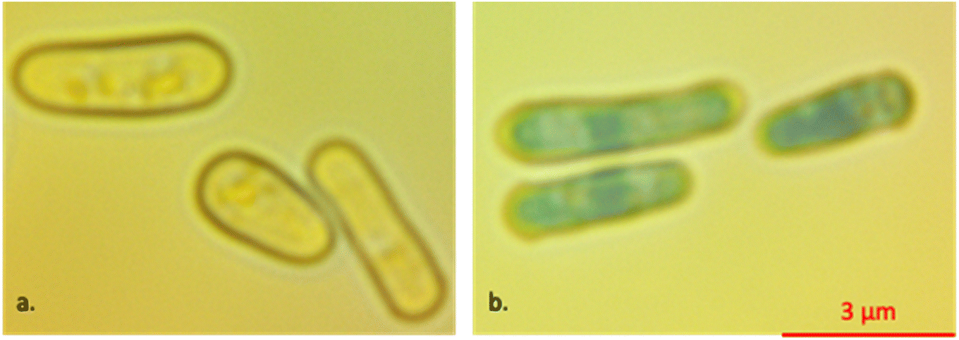 | ||
| Fig. 1 Comparison between (a) live and (b) dead yeast in the presence of methylene blue 0.23 v/v% inside the sucrose/dextrose solution. The scale bar is the same for both images. | ||
CPW design and fabrication
A 50 Ω CPW was designed as previously reported.44 To fine-tune and verify our calculations, we simulated the CPW with three sets of transmission lines using ANSYS high-frequency structure simulator (HFSS) software (Fig. S2†). The CPW has a 16 μm gap between the signal and ground electrodes. The signal electrode is 200 μm wide, and the electrodes taper to a 3 μm gap to focus the electric field inside the cell (Fig. 2a). Accordingly, the ratio between the cell and detection volume, and the consequent impedance change increased. In the fabrication process, we chose fused silica as a substrate due to its biocompatibility with biological materials, its transparency for observing cell manipulation, and its low loss tangent in the wide frequency range. Gold was chosen to be the metal layer of the sensor also because of its biocompatibility. The fabrication process involved a 1 μm photoresist AZ nLOF 2020 was spin-coated on the 500 μm thick 4 inch fused silica substrate. Then, metal layers (20 nm Ti/500 nm Au) were deposited on the substrate by an electron beam evaporator, followed by the lift-off metallization process to remove the undesired metal layers and the rest of the photoresist structure (Fig. 2b). Afterward, the PDMS microfluidic channel was bonded to the CPW using plasma bonding to ensure a leak-proof bond (Fig. 2c). The microfluidic channel's length, width, and height were 5 mm, 0.27 mm, and 20 μm, respectively. Finally, the CPW input and output were terminated by SMA coaxial connectors. | ||
| Fig. 2 (a) Schematic top view of CPW (b) microfluidic device integrated with CPW fabrication process (c) description of sealing the microfluidic channel on the substrate. (d) Schematic of the oscillatory system. | ||
Experimental setup
For visualization purposes, the device-under-test (DUT) was placed on top of a Nikon Eclipse Ti-E inverted fluorescence microscope (Fig. S3†). An Andor camera was then connected to the microscope for optical and electrical measurement. The DUT is connected to a Hewlett Packard 8753D vector network analyzer (VNA) through a pair of SMA connectors. All electrical signals are generated and measured in the S parameters by the VNA, from 30 kHz to 6 GHz. The VNA is calibrated using the short, open, load, and thru (SOLT) standards of a Maury-Microwave-2.92 mm calibration kit prior to measurement to avoid any errors by the connections and cables between the VNA and DUT. We set the intermediate frequency (IF) bandwidth to 30 Hz and the number of points to 801 in VNA.Additionally, we used oscillatory microfluidics to initially focus the cells to the center of the microfluidic channel width45 (Fig. 2d). Each inlet and outlet of the DUT microfluidic channel was coupled with funnel-shaped reservoirs connected to 3-way solenoid valves (Spex VapLock,Vernon Hills, IL) to switch the direction of the fluid inside the channel. Cells were loaded in the inlet reservoir and brought into the channel until the outlet reservoir filled and was at the same fluid level as the inlet reservoir. Once the cells are inside the channel and are detected via microscope, a lower oscillation pressure and frequency is applied to solenoid valves switching the fluid flow direction between the two ports. Flow oscillations push and pull the cells back and forth until a single cell approaches the CPW gap and is captured by the DEP between the CPW signal sensor gap. Fluid flow and oscillation frequency are controlled by a pressure controller (Fluigent, LineUp Push–Pull Flow EZ Le Kremlin-Bicêtre, France) module and function generator (Siglent SDG1032X Arbitrary Waveform, Solon, Ohio), respectively. With this method, an operator can precisely control the speed and location of the cells inside the microfluidic channel by controlling the frequency, duty cycle (on (ton) and off (toff) periods), and applied pressure to the solenoid valves. The main advantage of this trapping system in the context of EIS measurements is that by focusing the cells on a center line within the channel, it provides an easy and reproducible method to trap a single cell between the CPW sensor gap and immediately bring the fluid flow to zero by switching the solenoid valves to the closed state. Therefore, a single cell can be captured, characterized, and released with a controllable trap-and-release system, and then repeated to measure the next target cell (Movie S1†). In our experiments, we applied a signal with a frequency of 5 Hz, a duty cycle of 0.5, and a pressure of 0.2 mbar to move the cells between each EIS measurement.
Equivalent circuit
The equivalent circuit of the coplanar waveguide (CPW) without trapped yeast consists of five components: a lumped section under the microfluidic channel; two separate distributed areas under the air and PDMS (Fig. 3a); a series capacitor (Cs); and two shunt capacitors (CG). Characteristic impedance (Z0, ZPDMS) and electrical lengths (θ0, θPDMS) represent the distributed sections for air and PDMS. The loss of the entire CPW is accounted for by frequency-dependent resistances R0. The S parameters measured by the VNA are characteristic of the microfluidic channel using air and sucrose (fluid of known permittivity). The shunt capacitance is defined by air or sucrose, depending on whether the channel is filled or unfilled. We defined a single-shell spherical model for yeast. This model considers a parallel circuit of capacitance and resistance for each cell layer. As such, the yeast equivalent has four circuit elements, including yeast membrane resistance (RYM), yeast membrane capacitance (CYM), cytoplasm resistance (RCP), and cytoplasm capacitance (CCP) (Fig. 3b). To measure yeast characteristics by S parameters from the VNA, the cell circuit is expanded by considering the CPW with a trapped yeast (Fig. 3c). When a single yeast is trapped between the CPW electrode gap, the yeast equivalent circuit is placed in parallel with Cs because the measurement provides information for both the cell and the solution between the CPW. The characteristic parameter values of the whole system, such as CG, remain constant and are taken from the equivalent circuit data, while the microfluidic channel is filled with sucrose solution (Fig. 3a). | ||
| Fig. 3 (a) Equivalent circuit of the coplanar waveguide (CPW) comprising distributed sections under PDMS and air (b) equivalent circuit of the yeast with 4 equivalent circuit elements comprising yeast membrane resistance (RYM), yeast membrane capacitance (CYM), cytoplasm resistance (RCP), and cytoplasm capacitance (CCP). (c) Equivalent circuit of the coplanar waveguide with a yeast-trapped between the CPW signal electrode gaps. | ||
When a single cell is trapped between the two sharp electrode points, the majority of the RF passes through the cell's cytoplasm. Accordingly, no extra sub-circuits are needed for the field to bypass through the layers of the yeast cell or to cross the electrode polarization layer. The equivalent circuits were implemented in advanced design system (ADS) software. First, the parameters were estimated in the circuit by initial guesses. Then, the S parameters were fitted to the experimental results. By adjusting the values, we optimized each parameter. In brief, the de-embedding process was carried out step by step for the device, then the isotonic solution, and finally, for trapped cells. To minimize the least squares error, we used gradient optimization.
The reflection and transmission coefficient for a cell trapped in a series configuration can be defined as:22
 | (1) |
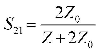 | (2) |
 where R is resistance, C is capacitance, and ω is angular frequency; therefore:
 | (3) |
 | (4) |
Data acquisition and measurement protocol
All of our measurements were done at room temperature. For the initial verification of the system, we measured the impedance of air and an isotonic solution of sucrose/dextrose with known permittivity. The impedance measurement across these fluids was recorded by the VNA using S parameters between the frequency range of 30 kHz to 6 GHz with the power of −18 dBm (Fig. 4). For verification, we used an optimization module in ADS software to simulate the reflection coefficient (S11) and the transmission coefficient (S21) and to predict the equivalent circuit elements.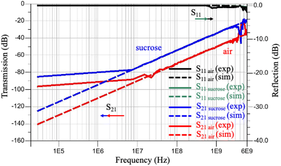 | ||
| Fig. 4 Comparison between measured reflection and transmission coefficients when the microfluidic channel was filled with air or a sucrose/dextrose solution consisting of 8.5 w/w% sucrose and 0.3 w/w% dextrose with simulation. Note: the reflection coefficient for air and sucrose overlapped for both the experiment and simulation. | ||
There was a good agreement between the experiment results (Fig. 4 – solid lines) and the simulation (Fig. 4 – dotted lines) except at low (<7 MHz) and high frequencies (>3 GHz). The reason for the discrepancy at very low frequency is due to the double layer effect between the cell and the electrodes at low frequency,46 and the equivalent circuit cannot justify the water dispersion at high frequency. In sum, the signals were not efficiently captured by R0. Therefore, there is no agreement between simulation and experimental results at low and high frequencies. However, as long as it does not affect the change between the S parameter measurement, we kept R0 in the equivalent circuit for simplicity.22 Besides, the difference between S21 measurements is more prominent than S11, which shows the sensitivity of S21 in this configuration with respect to S11. The values of the equivalent circuit parameters shown in this figure are listed in Table 1.
| Section | Parameter | Sucrose | Air |
|---|---|---|---|
| Microfluidic channel | C s (pF) | 3.5 | 0.6 |
| C G (fF) | 48.28 | 4.18 | |
| CPW under air | Characteristic impedance Z (Ω) | 53 | |
| Length@1 GHz θ air (°) | 1.19 | ||
| Loss R0 (Ω) | 10−9f (GHz) + 5 | ||
| CPW under PDMS | Characteristic impedance Z (Ω) | 46 | |
| Length@1 GHz θ PDMS (°) | 0.3 | ||
To ensure that our results are valid, we measured the background signal (measurement in the absence of yeast) every five minutes consecutively until the difference between the reflection and transmission line S parameters stabilized less than 0.001 dB. Cells inside the channel started to move toward the CPW within ∼10 μm steps by the oscillatory system, introduced inside the Experimental setup section. When the target single cell was close to the tapered gap between the CPW electrodes, we immediately brought the fluid flow to zero by switching the solenoid valves to the closed state, and the single cell was trapped between the electrodes by DEP along its long axis (Movie S2†). We captured the live cell by DEP at 4 MHz and 0 dBm and visually confirmed it using a microscope (Fig. 5). In the presence of DEP, the yeast cells moved toward the electrodes and were immobilized by the CPW. For the heat-killed yeast samples, due to the attraction of the dead yeast to the lower frequency, we captured single dead yeast by DEP at 30 kHz and 0 dBm.
 | ||
| Fig. 5 Micrograph of trapped yeast by dielectrophoresis (DEP) between the coplanar wave guide (CPW) electrode. | ||
After trapping the yeast, the VNA was quickly switched from the hold-frequency (4 MHz for live cell, 30 kHz for dead cell) to the sweep-frequency mode (30 kHz to 6 GHz) to measure the yeast's biophysical characteristics without the interference of the DEP. The commands were applied to the VNA using the Python code with the data analyzer. Two port scattering measurements were performed to obtain the single-cell electrical properties. The power was adjusted to −18 dBm, which is below the required power for reversible electroporation47 and to avoid any unwanted heating effect from microwave frequency.48 The cell remains immobilized between the CPW sensing gap, due to the coated lectin on the surface. The changes in S parameters were calculated and used to derive yeast biophysical characteristics using rapidly successive S parameters recorded with and without yeast. The yeast signal is defined as the difference between the reflection S11 and transmission coefficients S21 measured between the CPW with and without yeast trapped. With this type of measurement, the net effect of trapped yeast between the CPW will be acquired even with the calibration of the VNA shift with time. Transmission and reflection changes (Δ|S21|, and Δ|S11|) are calculated as follows:
Δ|S11| = 10![[thin space (1/6-em)]](https://www.rsc.org/images/entities/char_2009.gif) log|Sw/cell11|− 10log|Sw/o cell11| log|Sw/cell11|− 10log|Sw/o cell11| | (5) |
| Δ|S21| = 10log|Sw/cell21|− 10log|Sw/o cell21| | (6) |
Results and discussion
The impedance of ten live and twenty dead single yeast, individually, was measured while the single cell was trapped between the CPW signal electrodes. The averaged reflection S11 and transmission ΔS21 magnitude changes were measured for both live and dead yeasts (Fig. 6). To extract the electrical impedance values for the single yeast cell, the S parameters spectrum was fitted with the averaged experimental data based on the equivalent circuit changes with and without yeast trapped (Fig. 3). There was good agreement until ∼4 GHz, which showed the membrane and cytoplasm's electrical characteristics. Above 4 GHz, the suggested equivalent circuit is no longer valid as additional subcircuits inside the cell-equivalent circuit are required to define the nucleus's electrical properties. However, as the applied frequency range was insufficient for this purpose, we avoided adding additional subcircuits into the cell-equivalent circuit. | ||
| Fig. 6 (a) Reflection and (b) transmission magnitude changes for live and dead single yeast trapped between coplanar waveguide (CPW). | ||
The cell-equivalent-circuit values were optimized based upon the sensitivity of each parameter with its most prominent position on the simulation versus the frequency spectra as indicated by the arrows (Fig. 7). The direction of the arrows was intended to qualitatively show the incremental impact of each cell-equivalent circuit parameter at the frequency where the impact is most significant, that is, the positions of the arrows denote the frequency bands where each parameter is most sensitive. The values were optimized based on the trends, emphasizing different impedance parameters at various frequencies. Spectra for both the reflection changes and the transmission changes will undergo simultaneous adjustments during parameter tuning. Thus, it is essential for both spectra to reach an equilibrium to avoid overfitting in one spectrum and an off-target measurement in the other, which helps us to reach accurate data. At low frequency (kHz), signals can barely pass through the cell membrane due to the high value of membrane resistance and, therefore RYM is dominant. By increasing the frequency, due to the short-circuited yeast membrane capacitance, the membrane becomes transparent to the signal, and the cytoplasm's electrical properties can be calculated. The signal passes through the membrane (MHz) and RCP is dominated in that frequency range. The dominance of, CYM, and CCP appeared in the MHz and GHz frequency range. RYM's dominancy position region displays a more scattered region than the other equivalent parameter values (Fig. 6). This is due to the effect of solution conductivity at low frequencies. Although we used a low conductivity solution to decrease this effect at low frequency in our measurements, this effect is still noticeable. We calculated the membrane and cytoplasm electrical properties based on the ADS software's gradient optimization technique; their parameter values are listed in Table 2.
 | ||
| Fig. 7 Equivalent circuit parameters sensitivity with respect to the frequency in S-parameter spectrum for (a) reflection and (b) transmission changes up to 4 GHz. The circuit elements comprise yeast membrane resistance (RYM), yeast membrane capacitance (CYM), cytoplasm resistance (RCP), and cytoplasm capacitance (CCP). The direction of the arrows indicates each parameter's incremental effect at the frequency where the effect is most significant. | ||
| Parameter | Live yeast value | Dead yeast value |
|---|---|---|
| Membrane resistance RYM (MΩ) | 0.17 ± 0.08 | 0.29 ± 0.08 |
| Membrane capacitance CYM (pF) | 0.3 ± 0.1 | 0.023 ± 0.030 |
| Cytoplasm resistance RCP (MΩ) | 0.10 ± 0.04 | 0.24 ± 0.10 |
| Cytoplasm capacitance CCP (fF) | 3.6 ± 0.1 | 10.0 ± 0.1 |
| C s Live/Dead (pF) | 3.483 | 3.5 |
We gently killed the yeast cells by heating them which compromised the cell membrane integrity. No morphological changes between live and dead cells were discernible visually because the dead cell membrane was not completely broken down. Therefore, the inherent difference between live and dead cells was identified by EIS. Heated cells release most of their ion content, such as, K+, Mg2+ and Ca2+ into the solution through the perforations made in the membrane during the gentle heating process, as such, the permeability of the yeast membrane increases.49 Also, washing the cell with sucrose/dextrose solution will cause additional ions to be washed away, and therefore only a limited number of ions remain inside the cell membrane. Because the membrane is more permeable, however, the cell is porous and does fill with the solution surrounding it. As a result, the conductivity of the dead yeast membrane is going to be close to the sucrose/dextrose solution.50 Thus, the resistance of the dead cell membrane to the live cell membrane increases. Here, the amount of RYM increases from 0.17 ± 0.08 MΩ to 0.29 ± 0.08 MΩ. Cell membrane capacitance, which shows the dielectric property of the cell and cell integrity, remains constant while the cell is alive. However, it decreases due to cell death and drops to zero.51 The amount of CYM drops from 0.3 ± 0.1 pF for live yeast to 0.023 ± 0.03 pF for dead yeast. The higher value for live yeast CYM with respect to the dead cell reflects the membrane integrity of the live cell.
Changes in a dead cell's cytoplasm's electrical properties are a function of the media around the cell. Because the permeability of the dead cell membrane has increased, the media around the cell reaches the cytoplasm. Therefore, the conductivity of the cytoplasm is assumed to be close to the suspension media. This is consistent with literature reports where the resistance and capacitance of a dead cell cytoplasm in a buffer solution have been shown to decrease due to a greater amount of ion concentrations inside the solution with respect to the cell cytoplasm:52 While the electrical properties of the cytoplasm within a dead cell in a sucrose solution have been shown to increase due to the entrance of the non-conductive solution into the cell.53 In a separate experiment, we showed that the methylene blue dye penetrates the dead yeast cells indicating that the cell membrane was permeable after heat treatment of the cells (Fig. 1b). As a result, sucrose/dextrose solution is expected to substitute by ionic content inside the dead yeast cytoplasm, which allows the conductivity as well as the permittivity of the cytoplasm to approach the sucrose/dextrose solution value. Therefore, the conductivity of the dead yeast cytoplasm decreases.
As the cytoplasm permittivity is lower than the sucrose/dextrose solution,54 the permittivity inside the dead yeast cytoplasm increases as sucrose/dextrose solution concentration increases inside the dead cell. Thus, the dead cell cytoplasm resistance and capacitance due to the presence of sucrose/dextrose solution inside the cell increases, which is consistent with our observations. Here, the resistance of a dead yeast cytoplasm increases from 0.1 ± 0.04 MΩ to 0.24 ± 0.1 MΩ. Likewise, for the dead cell, as CCP/Live yeast < CCP/Dead yeast < Csurcose/dextrose due to the presence of sucrose/dextrose solution inside the dead cell cytoplasm, the capacitance of the dead yeast cytoplasm increases from 3.6 ± 0.1 fF to 10 ± 0.1 fF. The experimental data for live cells are in general agreement with the estimated theoretical values available in ESI† section. A comparison of our data and the reported literature can be found in Table S1.†
When live cells are trapped between the electrodes, due to the loading effect, the amount of Cs Live has to be lower than Cs = 3.5 pf. In this research, based on the optimization, we consider Cs Live = 3.483 pF, while Cs Dead = Cs = 3.5 pf due to the presence of sucrose/dextrose solution inside the cell and the loading effect can be neglected. The major difference between the dead and live cell signals appears in MHz and GHz, where the cytoplasm dominates in behavior with respect to the applied frequency (Fig. 7). This shows that, at higher frequency (GHz), microwave frequency can penetrate through the cell, as the membrane cannot act as an insulator anymore, and the difference between the intracellular properties will be more detectable. In this research, the noticeable difference appears at ∼3 GHz, where the cytoplasm capacitance dominates. Reflection and transmission phase changes for live and dead single yeast have been shown in Fig. S4.†
Based on the S parameters measurements, we showed that the change in cytoplasm structure can be identified within RF. The proposed system can speed up a continuous method for long-term measuring the target cell EIS measurement and checking the consecutive cell electrical measurement and viability. It provides a potential condition for investigating yeast growth between the CPW electrodes with the addition of an incubator and maintainable environmental growth conditions. Future work will focus on the EIS measurement of single-cell growth between the CPW to measure the structural changes during this period.
Conclusion
An innovative electrical-impedance sheathless microfluidic platform combined with CPW has been introduced to guide the cells with hydrodynamic focusing in a microfluidic channel and DEP was used to trap the single cell between the CPW electrodes. The electrical properties of the membrane and cytoplasm of single fission yeast S. pombe were investigated in a wide frequency range of 30 kHz to 6 GHz non-invasively. The electrical properties of the cell were measured through the suggested equivalent circuit simulation. We measured the cytoplasm's small capacitance to be approximately 3.6 fF. Then, the cell viability was successfully distinguished through impedance measurement. For dead cells, the resistance increases and the capacitance decreases due to the diffusion of the sucrose/dextrose solution through the perforated cell membrane. Also, the resistance and capacitance of the cytoplasm of the dead cell increases because of an increase in the permeability of the membrane and the influx of the surrounding media (sucrose/dextrose) to the cell cytoplasm. Noticeable differences between the viable and nonviable single yeast appeared at 3 GHz, where cytoplasm capacitance dominates. This system offers a rapid, precise, noninvasive, and label-free method for the characterization of a single cell, which can open the doors to use for any type of cell and different electrode configurations regardless of the shapes and geometries for cell viability discrimination, real-time single-cell monitoring, and rapid, precise single-cell analysis.Data availability
Data for this publication is available at https://doi.org/10.5281/zenodo.12863742.Author contributions
A. F. was responsible for conceptualization, methodology, formal analysis, data curation, investigation, device design, device fabrication, software, writing – original draft, and review & editing; A. M. was responsible for conceptualization, methodology, investigation, device design, device fabrication, and writing – review & editing; M. J. A. was responsible for conceptualization device design, methodology, formal analysis, software, and writing – review & editing; J. C. M. H. was responsible for supervision, writing – review & editing; A. A. was responsible for project administration, funding acquisition, writing – review & editing, and supervision.Conflicts of interest
The authors have no conflicts of interest to declare.Acknowledgements
We would like to express our gratitude toward Dr. Qian Chen from the Department of Biological Sciences, University of Toledo, for sending the yeast strain, and Dr. Kelley Donaghy for editing this manuscript. This work was performed in part at the Cornell NanoScale Science & Technology Facility (CNF), a member of the National Nanotechnology Coordinated Infrastructure NNCI, which is supported by the National Science Foundation (Grant NNCI-2025233). This work made use of the facility of the Cornell Center for Materials Research (CCMR) with support from the National Science Foundation Materials Research Science and Engineering Centers (MRSEC) program (DMR-1719875). Additional funding was provided by the United States Army Combat Capabilities Development Command (proposal number: 78597-EL).References
- A. Schmid, H. Kortmann, P. S. Dittrich and L. M. Blank, Curr. Opin. Biotechnol., 2010, 21, 12–20 CrossRef CAS PubMed.
- J. A. Osterberg, N. Dahal, R. Divan, C. S. Miller, D. Moline, T. P. Caldwell, X. Yu, S. W. Harcum and P. Wang, IEEE Trans. Microwave Theory Tech., 2021, 69, 1875–1886 Search PubMed.
- N. Haandbæk, S. C. Bürgel, F. Heer and A. Hierlemann, Lab Chip, 2014, 14, 369–377 RSC.
- Y. Feng, H. Chai, W. He, F. Liang, Z. Cheng and W. Wang, Small Methods, 2022, 6, 2200325 CrossRef CAS PubMed.
- X. Zhang, A. Hatamie and A. G. Ewing, Curr. Opin. Electrochem., 2020, 22, 94–101 CrossRef CAS.
- L. Huang, P. Zhao and W. Wang, Lab Chip, 2018, 28, 2359–2368 RSC.
- E. P. Preece, F. J. Hardy, B. C. Moore and M. Bryan, Harmful Algae, 2017, 61, 31–45 CrossRef CAS.
- M. Barreiros Dos Santos, R. B. Queirós, Á. Geraldes, C. Marques, V. Vilas-Boas, L. Dieguez, E. Paz, R. Ferreira, J. Morais, V. Vasconcelos, J. Piteira, P. P. Freitas and B. Espiña, Biosens. Bioelectron., 2019, 142, 111550 CrossRef CAS PubMed.
- H. E. Kubitschek, Nature, 1958, 182, 234–235 CrossRef CAS PubMed.
- D. C. Grulke, N. A. Marsh and B. A. Hills, Br. J. Exp. Pathol., 1973, 54, 884–891 CAS.
- M. Mansor and M. Ahmad, Int. J. Mol. Sci., 2015, 16, 12686–12712 CrossRef CAS PubMed.
- Y. Feng, J. Zhu, H. Chai, W. He, L. Huang and W. Wang, Small, 2023, 19, 2303416 CrossRef CAS PubMed.
- Y. Feng, Z. Cheng, H. Chai, W. He, L. Huang and W. Wang, Lab Chip, 2022, 22, 240–249 RSC.
- J. C. M. Hwang, IEEE Microwave Magazine, 2021, pp. 78–87 Search PubMed.
- H. Morgan, T. Sun, D. Holmes, S. Gawad and N. G. Green, J. Phys. D: Appl. Phys., 2007, 40, 61–70 CrossRef CAS.
- T. Sun and H. Morgan, Microfluid. Nanofluid., 2010, 8, 423–443 CrossRef CAS.
- Y. Cui, W. F. Delaney, T. Darroudi and P. Wang, Sci. Rep., 2018, 8, 497 CrossRef PubMed.
- R. Bashir, Adv. Drug Delivery Rev., 2004, 56, 1565–1586 CrossRef CAS PubMed.
- G. M. Whitesides, Nature, 2006, 442, 368–373 CrossRef CAS PubMed.
- S. Patel, D. Showers, P. Vedantam, T.-R. Tzeng, S. Qian and X. Xuan, Biomicrofluidics, 2012, 6, 034102 CrossRef PubMed.
- H. Li, C. Multari, C. Palego, X. Ma, X. Du, Y. Ning, J. Buceta, J. C. M. Hwang and X. Cheng, Sens. Actuators, B, 2018, 255, 1614–1622 CrossRef CAS.
- X. Ma, X. Du, H. Li, X. Cheng and J. C. M. Hwang, IEEE Trans. Microwave Theory Tech., 2018, 66, 3690–3696 Search PubMed.
- C. Yi, Q. Zhang, C.-W. Li, J. Yang, J. Zhao and M. Yang, Anal. Bioanal. Chem., 2006, 384, 1259–1268 CrossRef CAS PubMed.
- H. Chai, Y. Feng, J. Zhu, X. Meng, F. Liang, J. Bai and W. Wang, ACS Sens., 2023, 8, 2681–2690 CrossRef CAS PubMed.
- X. Ma, X. Du, L. Li, H. Li, X. Cheng and J. C. M. Hwang, IEEE J. Electromagn. RF Microw. Med. Biol., 2020, 4, 37–44 Search PubMed.
- Y. Feng, L. Huang, P. Zhao, L. Fei and W. Wang, Anal. Chem., 2019, 91, 15204–15212 CrossRef CAS PubMed.
- A. Denzi, C. Merla, M. Casciola, J. C. M. Hwang, X. Cheng, F. Apollonio and M. Liberti, in 2016 38th Annual International Conference of the IEEE Engineering in Medicine and Biology Society (EMBC), IEEE, Orlando, FL, USA, 2016, pp. 4232–4235 Search PubMed.
- C. Honrado, P. Bisegna, N. S. Swami and F. Caselli, Lab Chip, 2021, 21, 22–54 RSC.
- D. Malleo, J. T. Nevill, L. P. Lee and H. Morgan, Microfluid. Nanofluid., 2010, 9, 191–198 CrossRef PubMed.
- B. Xu, Y. Shi, Z. Lao, J. Ni, G. Li, Y. Hu, J. Li, J. Chu, D. Wu and K. Sugioka, Lab Chip, 2018, 18, 442–450 RSC.
- J. Chen, Y. Zheng, Q. Tan, E. Shojaei-Baghini, Y. L. Zhang, J. Li, P. Prasad, L. You, X. Y. Wu and Y. Sun, Lab Chip, 2011, 11, 3174 RSC.
- H. Li, A. Denzi, X. Ma, X. Du, Y. Ning, X. Cheng, F. Apollonio, M. Liberti and J. C. M. Hwang, IEEE Trans. Microwave Theory Tech., 2017, 65, 3503–3511 Search PubMed.
- C. Ferguson, N. Pini, X. Du, M. Farina, J. M. C. Hwang, T. Pietrangelo and X. Cheng, Anal. Chim. Acta, 2021, 1173, 338678 CrossRef CAS PubMed.
- M. Farasat, E. Aalaei, S. K. Ronizi, A. Bakhshi, S. Mirhosseini, J. Zhang, N.-T. Nguyen and N. Kashaninejad, Biosensors, 2022, 12, 510 CrossRef CAS PubMed.
- K. Zhao, Larasati, B. P. Duncker and D. Li, Anal. Chem., 2019, 91, 6304–6314 CrossRef CAS PubMed.
- M. Zhang, G. Huo, J. Bao, T. Markovic, P. Van Dijck and B. Nauwelaers, Chemosensors, 2022, 10, 318 CrossRef CAS.
- A. Zhang, D. Kawashima, H. Obara and M. Takei, IEEE Trans. Microwave Theory Tech., 2021, 69, 4678–4688 Search PubMed.
- Y. Yang, H. Zhang, J. Zhu, G. Wang, T.-R. Tzeng, X. Xuan, K. Huang and P. Wang, Lab Chip, 2010, 10, 553 RSC.
- D. Spencer and H. Morgan, Lab Chip, 2011, 11, 1234 RSC.
- F. Sherman, in Methods in Enzymology, Elsevier, 2002, vol. 350, pp. 3–41 Search PubMed.
- W. M. Arnold, A. G. Gessner and U. Zimmermann, Biochim. Biophys. Acta, Gen. Subj., 1993, 1157, 32–44 CrossRef CAS PubMed.
- Y. Ning, C. Multari, X. Luo, C. Palego, X. Cheng, J. C. M. Hwang, A. Denzi, C. Merla, F. Apollonio and M. Liberti, IEEE Trans. Microwave Theory Tech., 2014, 62, 1905–1911 Search PubMed.
- D. Sinha, D. Ivan, E. Gibbs, M. Chetluru, J. Goss and Q. Chen, J. Cell Sci., 2022, 135, jcs259046 CrossRef CAS PubMed.
- G. Gonzalez, Microwave Transistor Amplifiers: Analysis and Design, 1984 Search PubMed.
- B. R. Mutlu, J. F. Edd and M. Toner, Proc. Natl. Acad. Sci. U. S. A., 2018, 115, 7682–7687 CrossRef CAS PubMed.
- H. P. Schwan, Ann. N. Y. Acad. Sci., 1968, 148, 191–209 CrossRef CAS PubMed.
- Y. Ning, X. Ma, C. R. Multari, X. Luo, V. Gholizadeh, C. Palego, X. Cheng and J. C. M. Hwang, in 2015 IEEE MTT-S International Microwave Symposium, IEEE, Phoenix, AZ, USA, 2015, pp. 1–3 Search PubMed.
- T. Chretiennot, D. Dubuc and K. Grenier, IEEE Trans. Microwave Theory Tech., 2013, 61, 972–978 Search PubMed.
- S. Guyot, P. Gervais, M. Young, P. Winckler, J. Dumont and H. M. Davey, Environ. Microbiol., 2015, 17, 2982–2992 CrossRef PubMed.
- M. Kriegmaier, M. Zimmermann, K. Wolf, U. Zimmermann and V. L. Sukhorukov, Biochim. Biophys. Acta, Gen. Subj., 2001, 1568, 135–146 CrossRef CAS PubMed.
- C. Palego, C. Merla, Y. Ning, C. R. Multari, X. Cheng, D. G. Molinero, G. Ding, X. Luo and J. C. M. Hwang, in 2013 IEEE MTT-S International Microwave Symposium Digest (MTT), IEEE, Seattle, WA, USA, 2013, pp. 1–3 Search PubMed.
- H.-L. Gou, X.-B. Zhang, N. Bao, J.-J. Xu, X.-H. Xia and H.-Y. Chen, J. Chromatogr. A, 2011, 1218, 5725–5729 CrossRef CAS PubMed.
- Y. Ning, C. Multari, X. T. Luo, F. P. Cristiano, D. F. Molinero, S. Cheng, X. Hwang and C. M. James, Proc. 43rd Eur. Microw. Conf., 2013, p. 478 Search PubMed.
- A. Denzi, C. Merla, C. Palego, A. Paffi, Y. Ning, C. R. Multari, X. Cheng, F. Apollonio, J. C. M. Hwang and M. Liberti, IEEE Trans. Biomed. Eng., 2015, 62, 1595–1603 Search PubMed.
Footnote |
| † Electronic supplementary information (ESI) available. See DOI: https://doi.org/10.1039/d5lc00043b |
| This journal is © The Royal Society of Chemistry 2025 |