
 Open Access Article
 This Open Access Article is licensed under a
 Creative Commons Attribution 3.0 Unported Licence
Light-based 3D printing and post-treatments of moulds for PDMS soft lithography†
Bastien
Venzac

LAAS-CNRS, CNRS, Toulouse, France. E-mail: bastien.venzac@laas.fr
First published on 7th April 2025
Abstract
Polydimethylsiloxane (PDMS) chips are still the workhorses of academic microfluidics. Their production requires the fabrication of moulds, commonly produced using clean-room technologies. Light-based 3D printing and in particular, vat photopolymerization, material jetting and two-photon polymerization are rising techniques for the fabrication of moulds for PDMS replication, thanks to their accessibility, fast prototyping time, and improving resolution. Here, we are first reviewing the possibility opened by 3D printing for soft lithography, with a focus on mould designs. Then, inhibition of PDMS curing by photosensitive resins will be discussed as the main technical hurdle of 3D printed moulds. Fortunately, mould post-treatments are efficient solutions to eliminate this curing inhibition, which we gathered in a large database of post-treatment protocols from the literature.
Introduction: soft lithography
Polydimethylsiloxane (PDMS) is one of the preferred materials for microfluidic chip fabrication in academia. Among the ten most cited microfluidic articles, seven were based on PDMS chips according to Web of Science. PDMS has several properties that made it such a material of choice: transparency in the whole visible spectrum, low auto-fluorescence,1 elastic and non-brittle behaviour,2 and gas permeability.3,4 After mixing a liquid base and a curing agent, PDMS cures and accommodates the shape of moulds in which it was poured, a technique called soft-lithography.5–7 The transfer of micro and nanoscale features from a large variety of materials has been demonstrated, thanks to a low shrinkage during curing (1–2%).8 Moulded PDMS is easily bonded to another PDMS, glass or silicon substrate using plasma bonding to create enclosed channels (see Fig. 1).9 The PDMS flexibility also helps to create leak-free connections, by inserting large tubing inside a punched inlet. | ||
| Fig. 1 Schematic of the workflow of 3D printing for soft lithography. a) Stereolithography printing of a mould. b) Ink-jet printing of a mould. c) 2PP printing of a mould. d) Post-treatments, PDMS moulding and bonding of the PDMS replica on a glass slide for microfluidic chip fabrication. | ||
However, PDMS also presents several disadvantages, including low chemical resistance and high swelling when in contact with a large variety of organic solvents,10 strongly limiting its use for organic chemistry. Hydrophobic molecules easily adsorbs to the PDMS surface, and small hydrophobic molecules can also be absorbed inside the material.11,12 Surface treatments are often temporary, due to the migration of free silicone chains at the surface.13 Finally, soft lithography does not fit well for industrialization, as manufacturers prefer techniques allowing mass production like injection moulding or embossing.14 Despite the development of a wide variety of new materials for microfluidic fabrication which answer some of these critics, PDMS might still be used abundantly in the future, due to the inertia for the adoption of new materials and the over-presence of PDMS in laboratories and the literature.15
One of the main reasons for its predominance in academia, specifically, is the possibility of creating microfluidic chips outside clean room environments with limited equipment. One silicon mould could be replicated in hundreds of chips using soft lithography, reducing the consumed time and price in clean rooms. PDMS replicas have also been used as intermediate moulds for further replication in harder materials (fused silica, thermoplastics, …).16,17 Soft lithography has been tested with various mould types, including etched silicon, SU8 patterns on silicon,18 micro-milled brass or thermoplastics,19 and even coins or leaves,20,21 the latest being clean room-free.
In the search for cheaper and more accessible fabrication methods, moulds have been built using 3D printers. Fused deposition modelling, where a material is extruded from a nozzle, was tested as soon as 2002 with a thermoplastic material.22 However, the low resolution of this technology impeded its adoption in the community, as surfaces contained 20–50 μm grooves and channels were hardly smaller than 500 μm with badly defined sections.23 Since 2012, three 3D printing techniques based on photo-polymerization of resins have been more and more frequently employed for mould fabrication: vat photo-polymerization (VP), material jetting (MJ) and two-photon polymerization (2PP). In this review, we will first describe in detail these 3 techniques. In a second section, examples of moulds will be provided and listed in increasing complexity, starting with 2D moulds, then 2.5D moulds producing a single plane of networks with different heights, and finishing with PDMS chips with multiple layers and fully 3D networks. Discussion about the perspectives of 3D printing for soft lithography will be presented. Finally, in a last section, a large database of post-treatment protocols for 3D printed moulds will be presented, to avoid both classical problems of PDMS curing inhibition and difficult removal of the PDMS replicas from the moulds.
Section 1: light-based 3D printing techniques for soft lithography
Vat polymerization
In vat polymerization, a thin layer (between 10 and 100 μm) of resin is photo-polymerized between a mobile build plate and a transparent tank. The light is patterned using a scanning laser in the case of stereolithography (SLA) or a projected image shaped by a micro-mirror array (Digital Light Processing, DLP) or by a liquid crystal display (LCD) screen masking the light from LEDs, with wavelengths between 350 and 550 nm (with a majority of printers at 405 nm). The photosensitive resins are mostly composed of acrylate or methacrylate monomers with additives, including photo-initiators and light absorbers. The platform then moves up by a layer thickness, and a new layer is polymerized below the previous one (see Fig. 1a). When overhangs are created, the thickness of the layer is given by the penetration length of the light, which depends on the dose and the concentration of light absorbers.VP use for soft lithography has been rising since 2015; nowadays, VP printer prices are ranging from 200€ (Elegoo or Anycubic) to several tens of thousands of euros, with resolution going down to 30 μm for standard commercial printers and below for academic prototypes or high resolution commercial machines.24–26 For SLA, the print resolution and time are linked to the width of the laser beam, laser power and laser scan speed. Reducing the laser beam improves the resolution but increases strongly the printing time. Printing time is reduced using higher scanning speeds, but lead to lower doses which have to be compensated by a stronger laser. At the price of longer prints, both highly resolved and large moulds could be printed. In DLP printers, the resolution is directly linked to the pixel size of the projected image. Printing time is usually shorter than SLA, as a whole layer is cured in one exposure, and depends on the exposure time and light power. However, the print surface is dependent on the pixel number of the digital micro-mirror chips and manufacturers only provide chips with a resolution of up to 4 K (3840 × 2160 pixels).27 Therefore, a compromise between the print surface and resolution is mandatory. The last available technology, LCD printers, uses an LCD screen to mask light from LEDs. These low cost printers present the same advantages as the DLP printers, with the possibility of stitching several LCD screens to increase the print surface while keeping an identical resolution and low prices. However, these low-cost printers suffer from higher light inhomogeneity and lower power density, leading to lower performances and higher printing times.28
VP is an anisotropic fabrication process: the horizontal surfaces printed against the tank surface present a lower roughness than the vertical surfaces. In horizontal surfaces, small defects could be produced for SLA between laser passes if the hatching (the distance between two laser trajectories) is too high. Defects appear in DLP or LCD at the pixel borders, since the light dose is often not fully constant from the pixel center to its borders. For VP in general, the tank surface are never totally flat, with a roughness of around 100 nm for a Formlabs 3B SLA printer and 200 nm for an Anycubic Photon DLP printer.29 In vertical surfaces, grooves up to several tens of microns appear due to the vertical layers: in a single layer, the dose decreases along the light path thanks to light absorbers, leading to slight over-curing in the horizontal dimensions at the beginning of a layer.30 Manufacturers often recommend tilting large horizontal surfaces to avoid suction on the tank when the build plate moves up, but this configuration produces a stair-like surface with steps having the same dimensions as the layers. Therefore, moulds are mostly printed horizontally, sometimes vertically,30 with a limit on the total mould dimensions due to this suction effect that detaches the mould from the build plate. A usual solution to improve the adhesion to the build plate is to over-cure the first layers of the print. However, this over-curing also increases the shrinkage of the resin. If the mould is printed directly on the build plate, it results in a warped mould due to differential stress between the over-cured base and the rest of the mould.31 This warping is reduced by increasing the mould thickness, or by adding support pillars and a base between the mould and the build plate to obtain a homogeneously cured mould.
After completion of the printing, the resulting object has to be removed from the build plate and washed to remove the unpolymerized resin, usually using isopropanol – some recent resins are washed with water.32,33 Finally, most manufacturers recommend UV post-curing of the object, in order to fully complete the resin polymerization and improve the mechanical properties of the object.
Material jetting
In MJ, an on-demand piezo-based print-head similar to an inkjet printer ejects drops of photosensitive resins on a horizontal surface. The print-head is able to move horizontally in 2 dimensions and deposit drops down to 16 μm in diameter directly as lines of hundreds of droplets. After deposition, the resin is immediately cured by UV light located on the print-head. In this review, we will only describe inkjet printers working with photo-crosslinkable resins – other techniques used for 3D printing include the cooling of wax-based resins, the heating of thermoset drops or even the freezing of water-based resins.34,35 Therefore, the resin has several requirements: low viscosity for the ejection of a drop with the appropriate diameter, a large increase of this viscosity on the cooled build plate to avoid the flowing of the printed layer, and photo-curing chemistry (often based on acrylate and urethane).36 A subsequent layer of resin is then superimposed on the cured one until the print is finalized (see Fig. 1b). When overhanging structures have to be built, the use of a sacrificial support material is required. Deposited from different nozzles in the same print-head, the support material is usually composed of water soluble resin, based on polyethylene glycol (Stratasys process) or on heat-removable wax (3D Systems process).35MJ printing was the first mature commercial technology, leading to numerous reports for fabricating moulds before 2017.37–41 All the examples found in the literature were based on commercial printers from Stratasys and 3D Systems, and their numbers decreased after 2017, as VP started to be more common and less expensive than MJ, where printers cost several tens of thousands of euros. In terms of performance, the lowest resolution obtained was around 100 μm, with structures more rounded than VP, while the printing time was higher than VP (comparison between a Polyjet Eden 260VS and a Miicraft+ for the same design: 30 min vs. 12 min).23
Two photon polymerization
For moulds containing small 3D features, below 50 μm, a high-resolution 3D printing technique called two-photon polymerization (2PP) emerged in 2012.42 In this technique, a drop of photosensitive resin is deposited on a horizontal surface, often a glass slide or a silicon wafer. A high numerical aperture objective focuses a light beam from a femtosecond laser inside the drop, either from the other side of the glass slide, or directly immersed in the resin drop. The resin does not cure at the wavelength of the laser but reacts with light having half this wavelength. Moreover, at the focal point of the laser, the photon density is particularly high, allowing simultaneous and non-linear absorption of two photons by the resin photo-initiators, leading to radical creation and photo-polymerization of the resin.43 Since this two photon absorption is highly localized in the focal point, the polymerized voxel could be as small as 200 × 200 × 600 nm3, and depends strongly on the objective used.44 In the first commercial printers, the focal point is displaced in the liquid resin with a piezoelectric stage, allowing 3D, highly-precise but rather slow displacement with the unique possibility of following out-of-the-plane trajectories. In more recent generations, the focal point is displaced horizontally using galvanometric mirrors at high speed (up to 100![[thin space (1/6-em)]](https://www.rsc.org/images/entities/char_2009.gif) 000 μm s−1) and the object is therefore built in a layer-by-layer fashion. At the end of the print, the unpolymerized resin is developed by immersing the glass slide in solvents, usually propylene glycol methyl ether acetate and then isopropanol. One practical hurdle of 2PP is to preserve the adhesion of the print on the glass slide, as the resins could shrink up to 10%.45 This has been improved by silanizing the glass slide with methacrylated silanes, or by using other materials as supports (for example SU-8).46
000 μm s−1) and the object is therefore built in a layer-by-layer fashion. At the end of the print, the unpolymerized resin is developed by immersing the glass slide in solvents, usually propylene glycol methyl ether acetate and then isopropanol. One practical hurdle of 2PP is to preserve the adhesion of the print on the glass slide, as the resins could shrink up to 10%.45 This has been improved by silanizing the glass slide with methacrylated silanes, or by using other materials as supports (for example SU-8).46
While direct writing of solid epoxy resins has been demonstrated for the fabrication of microfluidic moulds since 2009,47 the spread of commercial 2PP printers, particularly from the Nanoscribe company, has given rise to numerous reports of mould fabrication in the literature since 2017. Printers are now able to print with voxels varying between 200 nm and 2 μm in width (Nanoscribe PPG2 and UpNano NanoOne 250). Identically to SLA, the same compromise has to be done between printing time and resolution. However, in contrast to SLA, the print size can be expanded in 2PP by stitching several fields of view, at the price of small defects at the stitching lines.44 In general, 2PP is still considered as a slow technique, especially at its smaller voxel size, as moulds for typical microfluidic networks still need printing time above 10 hours. Hybrid techniques have been published, where only the zones requiring high resolution were built using 2PP.48,49 The roughness of the prints depends mostly on the distance between two laser trajectories, and horizontal slices of 200 nm are observed.44 Optimized writing trajectories allowed the creation of moulds with roughness compatible with optical components.50
Replication in PDMS
After the mould is produced and developed, post-curing with UV-light is often used to improve the mechanical properties of the cured resin and to complete the conversion of the monomers, both in VP and 2PP.51 The classical soft-lithography process includes mixing of the PDMS base and the curing agent, pouring of the mix on top of the moulds and removal of air bubbles with vacuum. For MJ and VP, the produced moulds sometimes include millimetre-high walls around the channels to contain the PDMS, allowing also the PDMS height to be controlled.52,53 The PDMS is then usually cured at temperatures between 60 and 100 °C for several hours. Two main hurdles could then happen: for MJ and VP, most of the resins inhibit the PDMS curing, which is not the case for 2PP. Protocols have been developed to treat the moulds before pouring the PDMS, eliminating this curing inhibition. In section 3 of this review, we will discuss in detail the published post-treatments and propose an online and updated database of these protocols. These post-treatments are also sometimes required to facilitate the detachment of the PDMS replicas from the moulds. Among other tricks to improve the detachment, we advise to start detaching the PDMS from the resin mould with a scalpel, while adding isopropanol or ethanol below the replica. If the mould contains outer walls, an angle facilitates greatly the demoulding, as a lever can be produced with a scalpel on the side walls of the replica without damaging the horizontal surface. After removal of PDMS, the moulds could be re-used immediately.Section 2: examples of moulds
More and more laboratories are being equipped with 3D printers, and the temptation is high to 3D print moulds for soft lithography due to its numerous advantages compared to the main, classical clean room-based techniques. Infrastructure is not as heavy, except for 2PP which is still often located in clean rooms. The wide range of 3D printer resolutions could create features at the limits of UV-based photo-lithography (2PP) and features of several hundreds of micrometres in all directions, which are now the typical dimensions of microfluidic or millifluidic applications like organ-on-chips.54 Moulds comprising channels with different thicknesses or different geometries (rectangular, hemi-cylinders, half-spheres, …) are easily created, in a prototyping time of less than half a day from design to use, and for prices which continue to quickly decrease while performances keep increasing.In this section, we will give examples of the chip designs found in the literature using 3D-printed moulds, produced from VP, MJ or 2PP printers, starting with 2D moulds. Then, 2.5D moulds will be presented, showing already the great advantages of design freedom of 3D printing compared to lithography. More complex PDMS chips were produced using several moulds at once, allowing the fabrication of standing membranes and multilayer chips. The unique case of suspended channels with non-rectangular sections will then be discussed, finishing with the prospects of 3D printing for soft lithography.
2D moulds
A large proportion of the designs in the literature is still presenting channels with a single height, mimicking what is usual in classical photolithography, using SU-8 photoresists, dry films or other viscous, negative resists for thick patterns.55,56 3D printing use was mainly motivated by the simple access to this technology compared to clean-room techniques, its low prices or short prototyping times.57 It can be compared, here, to maskless lithography methods in terms of advantages over classical photolithography.56,58 Sometimes, chips with large channels, produced from macroscale moulds with features of several millimetres could simply not be done with clean-room techniques, limited to a few hundreds of micrometres.59 The argument of a limiting resolution for 3D printing is less and less valid, as VP is more and more precise, as seen in Fig. 2a with the creation of pillars down to 50 μm × 50 μm × 200 μm using a Sonic Mini 8K printer (Phrozen).52 Moreover, with 2PP, 2D moulds have been produced with the same resolution as photo-lithography, but with more defined walls and wells.60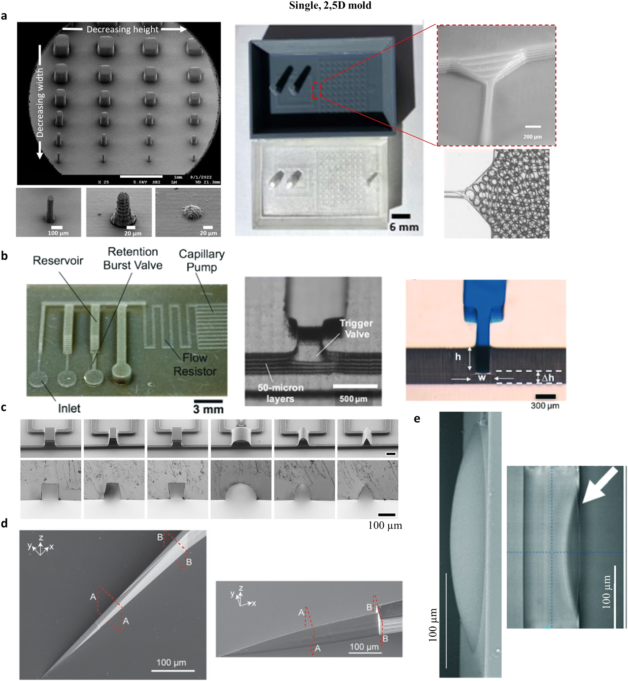 | ||
| Fig. 2 Examples of PDMS chips produced with a single, 2.5D mould. a) Left: Electronic micrograph of pillars produced with a Sonic Mini 8K (Phrozen) printer and Aqua Grey 8K (Phrozen) resin, showing pillars with setpoints of 75 × 75 × 500 μm3, 50 × 50 × 200 μm3, and 50 × 50 × 25 μm3. Middle and right: Mould and PDMS replica following a thermal and silanization post-treatment. Right: Multilayer channel used for step emulsification. Adapted from [A. Vedhanayagam, 2023 (ref. 52)]. b) Left: 3D-printed mould showing multiple channel heights (printer Perfactory MicroEDU, resin Envisiontec HTM140). Middle and right: Images of the replicated PDMS chip, after treatment with a silicone coating, and demonstration of the multilayer channel as a trigger valve for capillary microfluidics. Adapted from [Olanrewaju, 2016 (ref. 61)]. c) Micrographs of 2PP moulds and cut PDMS replicas of channels with different geometries produced by 2PP (Nanoscribe PPGT, IP-S resin). Adapted from [Lamont, 2019 (ref. 62)]. d) Microblades produced by 2PP (Nanoscribe PPGT2, IP-S resin). Adapted from [Koppaka, 2021 (ref. 63)]. e) Micrographs, side view of moulds produced by 2PP (Nanoscribe PPGT, IP-S resin) (left) and top view of the resulting PDMS channel. Adapted from [Tang, 2020 (ref. 50)]. | ||
2.5D moulds
A classical improvement of SU-8 lithography is the fabrication of 2.5D moulds by stacking several thicknesses of resin on top to each other. Such moulds are rarely made of more than 3 layers, as the fabrication time increases linearly for each new layer. 3D printing allows the simple fabrication of moulds having as many different thicknesses as wished. Resulting PDMS channels with steps were used for the trapping of superabsorbent particles,64 antibody-coated particles for diagnostics,65 and zebrafish embryos.66 For capillarity-based microfluidics, steps are efficient designs for trigger valves. Coupled with channels having different hydrodynamic resistance thanks to different heights, these valves are part of pump-free and programmable microfluidic circuitry able to flow several liquids sequentially for diagnostics (see Fig. 2c for pictures of the moulds and PDMS replicas).61Moulds with slopes and curves were even more complicated to fabricate using usual clean-room techniques. Greyscale lithography has been developed, whether using grey-tone masks or direct laser writing with different laser powers in SU-8.67,68 With 3D printers, moulds could present slopes and curves, as soon as the height of the structure is large compared to the slicing distance between two layers for VP printers, with the slices being less abrupt for MJ. As seen in Fig. 2a, a slope has been produced with a DLP printer to transfer droplets smoothly from a thin channel to a large reservoir. Here the slope is not fully smooth but presents more like a staircase profile due to the different layers.52 We used a similar slope to help the transfer of ex vivo testis tissue from a well to a channel.54 Slopes and curves have been used in several other applications, for example in hemi-cylindrical channels for valves (see Fig. 3a),69 pyramidal or hemispherical wells for aggregation of cells into organoids,70,71 or their fusions in well matrices,70,72 or even in patterned surfaces for the guiding of neurons.71
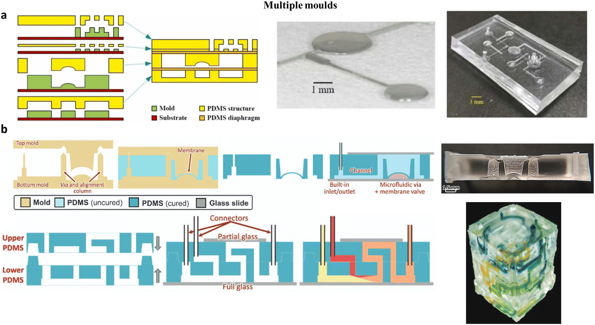 | ||
| Fig. 3 Examples of 3D PDMS chips produced using several moulds. a) Left: Schematic of the fabrication of the chip, using four different 3D printed moulds and stacking the resulting PDMS replicas with spin-coated membranes. Middle: Photographs of the 3D printed moulds, printed with a B9R-1-Cherry (B9Creations) resin and on a home-made DLP printer on a silanized glass slide, and then treated with extra UV and thermal curing. Right: Photograph of the final assembled chip. Adapted from [Liu, 2023 (ref. 69)]. b) Top left: Schematic of the one-step replication of a two-part mould with alignment structures printed with an MJ printer (ProJet 3000, 3DSystems and VisiJetEX200 resin) and treated with thermal baking and silanisation. Top right: Photograph of the resulting PDMS chip containing a membrane-based valve, cut in half. Bottom left: Schematic of the alignment of two 3D PDMS replicas produced with stacked moulds. Bottom right: Photograph of the resulting PDMS chips, made of 6 aligned layers. Adapted from [Glick, 2016 (ref. 41)]. | ||
Sometimes, really smooth slopes are required, and moving to 2PP printers is necessary as their slicing (when printing in a layer by layer fashion) is small enough to achieve gentle transitions.49,73,74 Several channel profiles, 100 μm-deep and wide, from rectangular, hemi-cylindrical or triangular were produced by Lamont et al. and successfully replicated into PDMS using a Nanoscribe printer with a layer height of 1 μm (Fig. 2c).62 Micro-blades, with several sharp profiles, have been produced with 2PP. Slopes with angles of 11° and an aspect ratio of 10:1 were produced and replicated, as seen in Fig. 2d.63 As a last example, 2PP also offers the possibility of finely tuning the shape of the PDMS channel wall themselves, for the fabrication of an optically smooth, 200 × 200 μm2 convex shape on the channel side for the creation of auto-aligned optical lenses (Fig. 2e).50
Assembling multiple replicas or moulds
PDMS microfluidic chips are often made of several stacked replicas from several moulds, for example for creating pressure-based valves by S. Quake et al.75 This simple idea was already presented in the first article showcasing the use of 3D printed moulds.37 Liu et al. pushed it further away for the production of a pressure regulator, composed of 4 different PDMS replicas sandwiching two thin PDMS membranes, as seen in Fig. 3a.69 Manufacturing the same chip using photolithography would have required a tedious process including four different wafers, one with two layers and one with three layers. With 3D printing, curved channels for valves and elaborated outlets for chip-to-world connection were easily added. Assembling several PDMS replicas around porous and/or elastic membranes to produce multilayer chips is also usual in the organ-on-chip area, following the first example of a lung-on-chip by Huh et al.76 This geometry has been produced from 3D-printed moulds, to mimic the lung,77 oviduct,78 or blood–brain-barrier culture conditions.79When stacking replicas, aligning the layers during bonding is cumbersome, especially for complex circuitry like the one in Fig. 3a. Using an MJ printer, Glick et al. proposed in 2016 a one-step moulding of “multilayer-like” PDMS chips by stacking two 3D-printed moulds (see Fig. 3b, top), for the production of valves.41 3D alignment structures facilitated the assembly of the moulds. PDMS was poured inside the double mould, cured and then released. Floors and ceilings of the channels were made by bonding glass slides. This technique had multiple advantages: auto-alignment of the layers, production of thin membranes without spin coating, and reduction of labour with a single moulding process. The replicas also contained alignment structures, facilitating their stacking into a 6-layer chip, with each layer having 3D channels (see Fig. 3b, bottom).
Suspended/3D moulds
In all the previous examples, the PDMS replicas were simply removed from 2.5D moulds by peeling them off. Cylindrical or even spiral channels have been produced by pulling out wires or fibres from cured PDMS, thanks to its elasticity.80,81 Using 3D-printed templates, the same process produced channels with irregular sections and shapes, as shown in Fig. 4a.40 Here, the mould was pulled out of the PDMS replica after removing the glass substrate below. This process also allowed the creation of channels with non-constant sections (Fig. 4b).53 A blood vessel with an aneurism has been scanned and replicated in negative as a suspended structure. The suspended structure has been printed inside a container by SLA. After pouring and curing the PDMS, the links between the container and the suspended structure were broken, the PDMS was unmoulded and the structure was removed thanks to the PDMS elasticity. This PDMS channel, mimicking the original vessel, has then been used to test the aggregation of platelets in this patient-specific geometry. Sometimes, controlling the external shape of the PDMS replicas was also required. Two studies proposed to combine an internal mould and an external mould to produce channels or tubes, with controlled wall thicknesses. In the first one, Hwang et al. produced soft robots, on which the wall thickness and geometry dictated the deflection of the robotic finger after pressurization of the internal channel.82 Karam et al. needed to control finely the wall thicknesses of models of blood vessels to mimic the vessel deformability under pressure.83 | ||
| Fig. 4 Examples of 3D PDMS chips produced from suspended structures. a) Left: Photograph of a PDMS replica containing one channel and one mould printed with an MJ printer (Objet24, Stratasys, and VeroWhitePlus resin) and coated with a gold–palladium layer. The mould was removed from the PDMS after curing. Right: Electronic micrograph of a channel cross section in PDMS. Adapted from [Hwang, 2015 (ref. 82)]. b) Left: Photographs of the mould printed using a SLA Perfactory 3 printer (EnvisionTec) and a PIC100 resin, treated with UV post-curing and washing in ethanol. Right: Blood perfusion inside a model of a stenotic vessel covered with endothelial cells to study the apparition of thrombosis. Adapted from [Costa, 2017 (ref. 53)]. c) Left: Schematic of the replication process. PDMS is partially cured on top of a 3D-printed mould containing suspended channels, printed using a Miicraft DLP printer and post-treated with thermal baking and silanisation. Before the complete curing of the PDMS, it is peeled off the master, forming a crack below the suspended channel which healed during the completion of the PDMS curing. Right: Example of crossing channels in the PDMS chip. Adapted from [Chan, 2015 (ref. 84)]. | ||
An interesting proposition, mixing 2.5 and 3D moulding, has been shown by Chan et al. Their VP mould comprised not only extruded structures on a base, like a classical 2.5D mould, but also short suspended bridges above other channels, as seen in Fig. 4c. Here, PDMS was slightly under-cured, so the replica could be peeled off the mould, at the price of a crack under the overpassing channel, corresponding to the liberation of the suspended bridge. However, thanks to the curing properties of the PDMS, these cracks healed during the completion of the curing, creating in a single step complex circuitry with multilevel channels, without any leakage.84
Perspectives and future of 3D printing for soft lithography
The use of 3D printers, and in particular VP, has skyrocketed in the last decade, pushed essentially by the increased availability of these printers in academic laboratories. Depending on the needs of each laboratory, the choice of the 3D-printing technology is crucial. Resolution in MJ is linked to the size of the ink drops, which depends on the nozzle geometry and viscosity of the ink. However, MJ printer optimization did not focus on resolution, but more on printing speed, print size and multi-material printing, with the last parameters being of small interest for mould manufacturing for soft lithography. Due to its large printing areas and printing speed, MJ printing is still a good choice when large-scale production of moulds with a resolution above 100 μm is required, at the cost of a more expensive printer.For VP, development has been more focusing on the resolution, where the smallest feature dimensions in X–Y depend mostly on the laser spot size for SLA or the pixel size for DLP. The resin composition, and in particular the presence of absorbers, has a larger influence on the z-resolution due to over-penetration of the light.35 The smallest features below 10 μm in X–Y have been demonstrated for projection micro stereolithography26,85 and for laser-based SLA.24 However, for one technology, decreasing the smallest feature dimensions always leads to a longer printing time. Recent advances in DLP demonstrated large area printed at sub-micron resolution, using stitching of the areas illuminated by a single micro-mirror array.26 Further shortening the printing time of VP would mostly be possible by tuning the resin reactivity.28
Another important feature of VP is simply its reduced price, allowing laboratories to invest into a low-cost printer. In 2024, printer prices started at around 200$ for Anycubic or Elego printers, with resolutions of 115 μm and 50 μm given by the supplier specifications, at the cost of illumination heterogeneity, low irradiance and inconsistent prints, inconveniences which have been partly reduced using optimized inks.28,86
To significantly decrease the resolution or printing time of moulds, one should check the development of other light-based 3D-printing technologies. Whereas commercial 2PP is still a slow printing technique compared to VP at its maximum resolution, numerous academic developments around this technology are significantly increasing its throughput, using multi-focus,87 two step-absorption,88,89 holographic 2PP,90 as reviewed by Balena et al.91 In another direction, several occurrences of volumetric 3D printing have been published since 2019, where volumes (and not layers) of resin are directly photo-polymerized through tomographic projections,92 or the intersection of two light beams of different colours, in combination with a dual colour photo-initiator.93 These strategies promised printing speed several orders of magnitude higher than VP, with resolution on the same scale.
In conclusion of this section, light-based 3D printing has already proven useful for the fabrication of mould for soft lithography. With the next generations of technologies, including more precise VP, high-speed 2PP or volumetric printing, 3D printing might overcome clean-room based mould fabrication techniques, as the smallest printable features and printing time will continue to decrease.
Section 3: PDMS curing inhibition by 3D printed moulds: protocol database
Is everything so easy with 3D printing? Not necessarily. In fact, one of the main drawbacks of VP and MJ is that PDMS does not cure correctly when in contact with most of their resins, leading to a layer of uncured PDMS around the channels that makes the mould useless. The main commercial silicone, Dow Corning Sylgard 184, is a complex mixture which contains a mix of linear polydimethylsiloxane with vinyl ends, branched siloxanes and platinum-based catalysts.94 On the other hand, commercial VP and MJ resins are industrial secrets, but most resins are based on radical systems, mostly (meth)acrylates or thiol-ene, sometimes mixed with cationic systems, like epoxides, oxetanes or vinyl ethers.35 We checked the composition of 12 resins from 12 different suppliers through their SDS documents: Anycubic Standard resin+,95 3D systems Eggshell AMB 10,96 B9Creations B9R-1-Cherry,97 DWS DL260,98 Elegoo ABS-like,99 Envisiontec PIC100,100 Formlabs Clear v4,101 Fun-To-Do Industrial Blend,102 LiqCreate Premium Tough,103 Phrozen Aqua Grey 8K,104 Resione HT100,105 and Stratasys VeroWhite+ RGD835.106 All of them reported the presence of acrylate or methacrylate monomers, with additional epoxy monomers for 3 of them. 9 SDS out of 12 indicated the presence of phosphine oxide-based photo-initiators. Care has to be taken as only “dangerous” chemicals are listed there.In the literature, several molecules have been shown to poison the platinum catalysts used in PDMS, including maleate, fumarate,107 β-alkynol,108 tri-organophosphite,109 or sulfur-containing molecules like benzothiazole.110 In particular, we have shown in a previous study that mixing phosphine oxide-based photo-initiators (TPO and BAPO) with PDMS resulted in complete inhibition of the silicone curing.111 This analysis was supported by other experiments, showing that the leaching of fragments of phosphine oxide-based photo-initiators from the moulds to the PDMS is likely the cause of the PDMS curing inhibition from 3D-printed moulds. The absence of this class of photo-initiators in 2PP resins is probably the main reason for the absence of curing inhibition from these resins.35 We did not show any significant inhibition from monomers (methyl-methacrylate) but rather a stronger bond between a cured, acrylate-contaminated PDMS part and 3D-printed mould. Therefore, two effects of leachates from moulds have to be reduced with post-treatments: first, the PDMS curing inhibition and second, potential bonding between the PDMS and the printed mould.
This increase of bonding between 3D printed moulds and PDMS has been shown, independently of the PDMS inhibition, for a large spectrum of resin formulation. Coupled with the presence of a larger roughness on the vertical surfaces, demoulding PDMS can be tricky, and the literature contains many protocols to decrease this adhesion, using mostly fluorinated silanes, and release chemicals. This is also the case with 2PP moulds, where a slight increase of adhesion can break these fragile moulds due to the weak adhesion of the printed structures on the substrate (often a glass slide or silicon substrate).
In the next sections of this article, we propose to review all the protocols for treating 3D printed moulds and to class them into different classes of protocols. Since the first reported use of SLA-printed moulds in 2013 (ref. 37) and MJ-printed moulds in 2014,38,39 multiple protocols have been proposed to alleviate the PDMS curing inhibition observed with the vast majority of photosensitive resins. Most publications did not study in detail this phenomenon and proposed a simple protocol, without discussing its optimization. Some other studies, including ours, focused on that specific question.71,111,112 In total, at the submission of this review, we found in the literature 136 different post-treatments with enough details to be replicated, for 75 different resins. Here, we propose a review of the main routes used to treat 3D printed moulds and their mechanisms and offer a database containing all these protocols. Along this publication, we propose to maintain and expand further this list in the future as an open access database available at the following DOI: https://doi.org/10.5281/zenodo.13881893. New published protocols could be directly sent to the corresponding author at E-mail: bastien.venzac@laas.fr to be added into the database.
UV-post curing
VP manufacturers advise short post-curing of the print under UV light, at the same wavelength as the printer light, often at 405 nm. In order to obtain the best resolution, the light dose applied during printing is just above the polymerization threshold of the resin, meaning that only a fraction of the active sites of the monomers reacted. To improve the mechanical properties of the printed object and complete the resin polymerization, a UV post-curing step is often required, especially for (meth)acrylate systems.35,51 We have previously shown, using Raman spectroscopy of moulds, that UV post-curing reduced methacrylate and acrylate groups in the mould.111 One drawback of UV post-curing is the short penetration length of the light inside the printed objects, due to the necessary presence of photo-absorbers in the resin. UV post-curing might not reach the core of thick prints. Eleven post-treatments consisting only of UV-post curing have been found (see Table 1), almost all for VP, with treatment duration longer than the manufacturer recommendation for routine post-curing, from 15 min to 24 h.57,71,79,111,113–116 Unfortunately, the method sections of most articles are incomplete, with missing information on UV wavelengths, treatment duration and/or dose applied. Several articles used a commercial curing box, optimized for multi-angle illumination of prints and available at reasonable costs, making such a post-treatment step quite standard for labs equipped with VP 3D printers. Beware, UV wavelength is an important parameter, as 254 nm or 365 nm UV light does not often cure resins that polymerize at 405 nm.| Reference | Resin | UV post-curing | |||
|---|---|---|---|---|---|
| Duration | Wavelength | Dose | Temperature | ||
| X corresponds to data unavailable in the references. | |||||
| VAT photopolymerization | |||||
| Razavi Bazaz57 | Creative CADWorks, custom resin | X | 405 nm | X | X |
| Venzac111 | DWS, GL4000 | 4 h | 405 nm | 14 mW cm−2 | 60 °C |
| Venzac111 | Formlabs, Flex v1 | 2 h | 405 nm | 14 mW cm−2 | 60 °C |
| Hagemann71 | Phrozen, Aqua Grey 4K | 1 h | 405 nm | X | X |
| Vogt114 | Formlabs, Black RS-F2-GPBK-04 | 24 h | X | X | X |
| Cameron79 | Creative CADWorks, Master Mold Resin | 60–80 min | 405 nm | 5.5 mW cm−2 | RT |
| Cameron79 | Formlabs, Clear RS-F2-GPCL-04 | 1 h | 405 nm | 5.5 mW cm−2 | 60 °C |
| Lundquist113 | Formlabs, BioMed Clear | 1 h | 405 nm | 5.5 mW cm−2 | 60 °C |
| Som Yang115 | Formlabs, Clear FLGPCL04 | 15 min | 405 nm | 5.5 mW cm−2 | RT |
| Som Yang115 | Formlabs, Surgical Guide FLSGAM01 | 15 min | 405 nm | 5.5 mW cm−2 | RT |
| Material jetting | |||||
| Cutuli116 | Stratasys, Vero PureWhite RDG837 | 1 h | X | X | 37 °C |
Thermal baking only
Another classical post-treatment is a thermal baking step after the development of the moulds, at temperatures ranging from 60 to 200 °C. For cationic systems, heat has the same effect as UV post-curing and completes the polymerization of the monomers, with the advantage of treating also the printed part beyond the UV penetration length.35 In a previous study, we have shown that thermal baking of moulds for 4 different resins is accompanied by a decrease of mass around 1% and by the evaporation of a liquid containing mainly fragments of the photo-initiator, and sometimes (meth)acrylate monomers. When mixed with PDMS, this liquid inhibits the PDMS curing. We have also shown that thermal baking promotes the rearrangement of photo-initiator fragments into larger molecules.111 Therefore, thermal baking could limit the PDMS curing inhibition through two phenomena: evaporation of small fragments of phosphine oxide-based photo-initiators outside of the moulds and trapping of the remaining fragments inside the moulds to limit their leaching. Fourteen different post-treatments have been sorted, for eleven different resins, as seen in Table 2. Compared to UV-curing, only an oven or a hotplate is necessary for this simple treatment. The choice of temperature and duration has to be tested by trial and error, starting with a high temperature of around 100–120 °C and at least 4 hours, and then reducing the duration or temperature if the treatment is efficient. However, high baking temperature could significantly wrap or even crack moulds for some resins, especially without UV post-curing. Fortunately, lower baking temperatures are usually also efficient, at the price of longer treatment durations. Indeed, we have observed that an imperfectly treated mould would stop inhibiting the PDMS curing after several rounds of PDMS baking (usually 60 °C, minimum 2 hours).| Reference | Resin | Thermal baking | |
|---|---|---|---|
| Duration | Temperature | ||
| VAT photopolymerization | |||
| Venzac111 | DWS, DL260 | 1 h at 120 °C or 24 h at 60 °C | |
| Venzac111 | DWS, DS3000 | 2 h at 120 °C or 24 h at 60 °C | |
| Venzac111 | Envisiontec, E-shell 300 | 1 h at 120 °C or 24 h at 60 °C | |
| Venzac111 | Formlabs, Black v1 | 1 h at 120 °C or 24 h at 60 °C | |
| Venzac111 | Formlabs, Clear v1 | 1 h at 120 °C or 24 h at 60 °C | |
| Venzac111 | Formlabs, Flex v1 | 2 h | 120 °C |
| Venzac111 | Formlabs, High Temperature v1 | 1 h at 120 °C or 1 h at 60 °C | |
| Kang117 | Formlabs, Clear | 1 h | 120 °C |
| Sanchez118 | Formlabs, Black | Overnight | 60 °C |
| Material jetting | |||
| Stolovicki119 | Objet, unspecified | Overnight | 90 °C |
| Cicolini120 | Stratasys, VeroWhite | Overnight | 110 °C |
| Segantini121 | Stratasys, VeroWhite | 12 h | 110 °C |
| Mossoti122 | Stratasys, VeroWhite | Overnight | 110 °C |
| 2-Photon polymerization | |||
| Tang50 | Nanoscribe, IP-S | 2 h | 200 °C |
Combination of UV post-curing and thermal baking
For most VP resins, a single UV post-curing or thermal baking step is not enough to eliminate the leaching of curing inhibitors out of the moulds. This is why numerous post-treatments for VP (43 in Table 3) combine a first post-curing step with a thermal baking step. In total, 33 resins were treated using UV post-curing, thermal baking, or a combination of both treatments, making such a protocol a legitimate candidate for a title of “universal” post-treatment for VP resins. Such a combination has one strong advantage: its accessibility. A UV curing box is often sold with 3D printers, and an oven or a hotplate is a classical piece of equipment in most labs.| Reference | Resin | UV post-curing | Thermal baking | ||||
|---|---|---|---|---|---|---|---|
| Duration | Wavelength | Dose | Temperature | Duration | Temperature | ||
| X corresponds to data unavailable in the references. | |||||||
| VAT photopolymerization | |||||||
| Dinh123 | Da Vinci Nobel 1.0A resin | X | X | X | X | 24 h | 80 °C |
| Grigorov112 | Anycubic, basic | 4 min | 395 nm | X | X | 1 h | 80 °C |
| Grigorov112 | Anycubic, plant based | 4 min | 395 nm | X | X | 1 h | 80 °C |
| Grigorov112 | Elegoo, ABS-like | 4 min | 395 nm | X | X | 2 h | 80 °C |
| Grigorov112 | Phrozen, Aqua 4K | 4 min | 395 nm | X | X | 2 h | 80 °C |
| Jóskowiak124 | Formlabs, Grey | 1 h | 405 nm | 5.5 mW cm−2 | 60 °C | 72 h | 65 °C |
| Karam83 | 3D Systems, Eggshell-Amb10 | 90 min | X | X | X | 1 h, 60 °C before UV/30 min, 80 °C after UV | |
| Lee125 | Formlabs, Clear v4 | 1 h | X | X | X | 2 h | 120 °C |
| Liu69 | B9Creations, B9R-1-Cherry | 1 h | X | X | X | 1 h | 100 °C |
| Može | Fun-to-do, Industrial Blend Unpigmented | 6 min | 365–405 nm | 900 mW cm−2 | X | 4 h | 100 °C |
| Može | Fun-to-do, Deep Black | 6 min | 365–405 nm | 900 mW cm−2 | X | 4 h | 100 °C |
| Može | Phrozen, Aqua Grey 8K | 10 min | 365–405 nm | 900 mW cm−2 | X | 4 h | 100 °C |
| Memarian126 | Phrozen, Aqua Gray 8K | 45 min | X | X | RT | 4 h | 100 °C |
| Le Gac127 | Formlabs, Clear v4 | 1 h | 405 nm | 5.5 mW cm−2 | 60 °C | 2 h | 120 °C |
| Le Gac127 | Formlabs, High Temp v2 | 2 h | 405 nm | 5.5 mW cm−2 | 60 °C | 4 h | 120 °C |
| Le Gac127 | Formlabs, BioMed | 30 min | 405 nm | 5.5 mW cm−2 | 60 °C | 2 h | 120 °C |
| Le Gac127 | Formlabs, surgical grade | 1 h | 405 nm | 5.5 mW cm−2 | 60 °C | 2 h | 120 °C |
| Le Gac127 | Formlabs, Elastic 50A | 6 h | 405 nm | 5.5 mW cm−2 | 60 °C | 48 h | 120 °C |
| Le Gac127 | Anycubic, plant-based | 1 h | 405 nm | 5.5 mW cm−2 | 60 °C | 2 h | 120 °C |
| Le Gac127 | Elegoo, plant-based | 1 h | 405 nm | 5.5 mW cm−2 | 60 °C | 2 h | 120 °C |
| Le Gac127 | eSUN, eResin | 1 h | 405 nm | 5.5 mW cm−2 | 60 °C | 2 h | 120 °C |
| Le Gac127 | BASF, Ultracur3D RG 35 | 1 h | 405 nm | 5.5 mW cm−2 | 60 °C | 2 h | 120 °C |
| Le Gac127 | BASF, Ultracur3D ST 45 M | 1 h | 405 nm | 5.5 mW cm−2 | 60 °C | 2 h | 120 °C |
| Ramasamy29 | Anycubic, Black (SKU TL4425) | 30 min | 405 nm | 5.5 mW cm−2 | 60 °C | 2 h | 120 °C |
| Ramasamy29 | Formlabs, Clear v4 (RS-F2-GPCL-04) | 30 min | 405 nm | 5.5 mW cm−2 | 60 °C | 2 h | 120 °C |
| Venzac111 | DWS, GL4000 | 1 h | 405 nm | 14 mW cm−2 | 60 °C | 8 h | 120 °C |
| Venzac111 | DWS, GM08 | 1 h | 405 nm | 14 mW cm−2 | 60 °C | 8 h at 120 °C or 24 h at 60 °C | |
| Venzac111 | Envisiontec, PIC100 | 2 h | 405 nm | 14 mW cm−2 | 60 °C | 4 h | 120 °C |
| Venzac111 | Envisiontec, R11 | 2 h | 405 nm | 14 mW cm−2 | 60 °C | 4 h | 120 °C |
| Venzac111 | Fun-to-do, Deep Black | 15 min | 405 nm | 14 mW cm−2 | 60 °C | 2 h at 120 °C or 48 h at 60 °C | |
| Venzac111 | Fun-to-do, Industrial Black | 15 min | 405 nm | 14 mW cm−2 | 60 °C | 2 h | 120 °C |
| Venzac111 | Fun-to-do, Industrial Red | 15 min | 405 nm | 14 mW cm−2 | 60 °C | 2 h at 120 °C or 48 h at 60 °C | |
| Venzac111 | Fun-to-do, Standard Black | 1 h | 405 nm | 14 mW cm−2 | 60 °C | 4 h | 120 °C |
| Venzac111 | Fun-to-do, Standard red | 2 h | 405 nm | 14 mW cm−2 | 60 °C | 8 h | 120 °C |
| Yang128 | Cyanate custom resin with a perfluoropolyether release agent | 20 min | X | 3 mW cm−2 | X | 1 h at 100 °C then 2 h at 140 °C then 2 h at 160 °C then 2 h at 180 °C then 2 h at 200 °C | |
| Som Yang115 | Formlabs, Elastic 50A (FLELCL01) | 15–45 min | 405 nm | 5.5 mW cm−2 | RT | 8 h | 80 °C |
| Som Yang115 | Formlabs, Elastic 80A (FLFL8001) | 15–45 min | 405 nm | 5.5 mW cm−2 | RT | 8 h | 80 °C |
| Ye66 | Anycubic, Gray UV | 2 h | X | X | X | 16 h | 80 °C |
| Hu129 | Formlabs, Clear | 30 min | X | X | X | 2 h | 120 °C |
| Lee130 | 3D Systems, Nextdent Ortho Rigid | 1 h | X | X | X | 2 h | 100 °C |
| Khoo131 | Formlabs, Clear v4 resin (RS-F2-GPCL-04) | 30 min | 405 nm | 5.5 mW cm−2 | 60 °C | 1 h | 120 °C |
| Chen132 | Formlabs, Durable | 30 min | 405 nm | 5.5 mW cm−2 | RT | 24 h | 65 °C |
| Byrne133 | Formlabs, Clear resin | 15 min | 405 nm | 5.5 mW cm−2 | RT | 3 h | 130 °C |
Mould surface coating
Coating the moulds with a protective layer that limits or suppresses the diffusion of inhibitors is also an efficient strategy. In our database (Table 4), 23 different coatings are referenced; some of them aim at reducing the PDMS curing inhibition, especially when applied without any other post-treatments. The coating could also improve the surface roughness of the mould, simplifying the optical imaging through a moulded PDMS part, or the plasma bonding of PDMS on another substrate, when applied after UV post-curing or thermal baking. In more detail, silicone, ink and lacquer were applied by manual airbrushing, with thicknesses of up to 50 μm. Parylene has been applied by vacuum deposition, with a thickness down to 18 nm. Finally, high-tech, clean room processes have also been tested, including aluminium, platinum, palladium and gold sputtering, SiO2 coating, SU-8 spin-coating and plasma-based Teflon deposition. When choosing a coating, care has to be taken about the following parameters: price of the equipment, reproducibility of manual operation like airbrushing, comparison of the thickness of the coating and the smallest feature printed in the mould, and preferential adhesion of the coating on the mould compared to PDMS, to avoid transferring it to the replica.| Reference | Resin | UV post-curing | Thermal baking | Coating | |
|---|---|---|---|---|---|
| Wavelength, dose, temperature | Duration, temperature | Material | Method | ||
| PFDTCS: trichloro(1H,1H,2H,2H-perfluorodecyl)silane. | |||||
| VAT photopolymerization | |||||
| Mohamed134 | Formlabs, Clear GPCL02 | Gold–palladium, 10 nm | Sputtering | ||
| Olanrewaju61 | Envisiontec, HTM140 | Silicone (ease release 200) | Spray | ||
| Escudero72 | DWS, DL260 | SiO2 (15 nm), then PFDTCS monolayer | Surface preparation deposition (Memsstar) | ||
| Hagemann71 | Anycubic, Clear | 1 h, 405 nm | Enamel paint (Plastikote), <50 μm | Airbrushing | |
| Hagemann71 | Elegoo, ABS-like | 1 h, 405 nm | Enamel paint (Plastikote), <50 μm | Airbrushing | |
| Hagemann71 | LiqCreate, Premium Tough | 1 h, 405 nm | Enamel paint (Plastikote), <50 μm | Airbrushing | |
| Hagemann71 | Phrozen, Water washable model gray | 1 h, 405 nm | Enamel paint (Plastikote), <50 μm | Airbrushing | |
| O'Grady70 | Formlabs, Grey | 1 min, 405 nm, 5.5 mW cm−2, 60 °C | Parylene, 18 nm | Vacuum deposition | |
| O'Grady70 | Formlabs, Clear | 1 min, 405 nm, 5.5 mW cm−2, 60 °C | Parylene, 18 nm | Vacuum deposition | |
| Comina37 | Miicraft, unspecified | 10 min | Ink (Pentel NN60) | Airbrushing | |
| Otroshchenko135 | Eryone, White water washable | 10 min, 405 nm | 6 h, 100 °C | PTFE | Sputtering with O2 or N2 plasma |
| Otroshchenko135 | Phrozen, TR250LV | 10 min, 405 nm | 6 h, 100 °C | PTFE | Sputtering with O2 or N2 plasma |
| Otroshchenko135 | Resione, G217 | 10 min, 405 nm | 6 h, 100 °C | PTFE | Sputtering with O2 or N2 plasma |
| Otroshchenko135 | Resione, HT100 | 10 min, 405 nm | 6 h, 100 °C | PTFE | Sputtering with O2 or N2 plasma |
| Byrne136 | Formlabs, Clear | 15 min, 405 nm, 5.5 mW cm−2, 60 °C | 2 h, 130 °C | Lacquer thinner (Klean-Strip) and clear coat (Finish 1 FC720/FH612), 40 μm | Airbrushing |
| Byrne136 | Formlabs, Grey | 30 min, 405 nm, 5.5 mW cm−2, 60 °C | 3 h, 130 °C | Lacquer thinner (Klean-Strip) and clear coat (Finish 1 FC720/FH612), 40 μm | Airbrushing |
| Dediu137 | Creative CADWorks, Master Mold Resin | 1 h, 405 nm | 20 h, 65 °C | Aluminum, 300 nm | E-beam high vacuum thin film deposition |
| Yi138 | Formlabs, High Temperature | 4 h | 1 h, 130 °C | Dry film lubricant (Electrolube) | Spray |
| Material jetting | |||||
| Guvanasen39 | Objet, Transparent Fullcure 720 | Gold (0.4 nm) and Knock Out Mold Release | Sputtering and painting | ||
| Chande139 | Stratasys, VeroBlack | SU-82002 | Spin-coating, soft-bake, UV exposure | ||
| Hwang140 | Stratasys, VeroWhitePlus | Platinum, 10 nm | Sputtering | ||
| Cairone141 | Stratasys, VeroWhitePlus 835 | Hydrosoluble acrylic acid polymers (Sokalan) | Drying on top of the mould | ||
| Hwang82 | Stratasys VeroWhitePlus RGD835 | Gold–palladium, 10 nm | Sputtering with different angles | ||
Silanization
Silanization is a specific type of coating which is often used with PDMS, glass or silicon in the microfluidics and microfabrication community, but has also been shown to be applicable to other substrates like metal or polymers. Usually, the substrate has first to be oxidized with a plasma treatment, and then a silane monolayer is formed by immersing the substrate in a silane–solvent solution or by vapour deposition. The silicon oxide part of the silane bonds to the oxidized substrate. In these post-treatment, the silanes used are perfluorosilane, adding a “Teflon-like” monolayer on top of the polymerized resin. Such a treatment reduces the PDMS curing inhibition and the bonding of the silicone on the acrylate surface (see Table 5). For this second objective, silanization has been added to previously described post-treatments. It has also been a popular treatment to help the detachment of PDMS replicas on 2PP moulds. The mechanism of the functionalization of acrylates by silane has not been studied. Is it classical grafting after plasma oxidation? Simply adsorption? One attention point: as being part of the eternal pollutant category, the use of fluorosilane might be restricted in the future. Fortunately, many alternatives to silanization are available for treatment of 3D-printed moulds.| Reference | Resin | UV post-curing | Thermal baking | Silanization | |
|---|---|---|---|---|---|
| Wavelength, dose, temperature | Duration, temperature | Plasma activation | Coating | ||
| PFOTCS: trichloro(1H,1H,2H,2H-perfluorooctyl)silane. PFOTES: 1H,1H,2H,2H-perfluorooctyltriethoxysilane. PFDTES: 1H,1H,2H,2H-perfluorodecyltriethoxysilane. | |||||
| VAT photopolymerization | |||||
| Zhang142 | Anycubic, unspecified | No | Immersion for 2 h in 1% wt PFOTES–ethanol | ||
| Liu143 | Anycubic, unspecified | 60 min | 2 h, 120 °C | 3 min | Spin-coating of PFOTCS |
| Credi144 | DWS, DL260 | 15 min, 2.1 mW cm−2 at 405 nm | 1 h, 100 °C | Air plasma, 150 W, 60 s | Immersion for 1 h in 1% PFDTES–toluene |
| Vedhanayagam52 | Phrozen, Aqua Grey 8K | 30 min | 1 h, 60 °C | No | Vapour deposition of PFOTCS for 25 min under vacuum |
| Han30 | Asiga, PlasCLEAR | 3 min (Asiga UV chamber) | 1 h, 120 °C, autoclave | Oxygen plasma, 1 min | Vapour deposition of PFOTCS for 2 h under vacuum |
| Chan84 | Miicraft, unspecified | 10 min | 4 h, 130 °C | Oxygen plasma, 3 min | Vapour deposition of PFOTCS for 30 min under vacuum |
| Wang145 | Asiga, PlasCLEAR v2.0 | 30 min | 48 h, 70 °C | No | Vapour deposition of PFOTCS for 2 h under vacuum |
| Material jetting | |||||
| King38 | Stratasys, VeroClear | 24 h, 80 °C | No | Vapour deposition of PFOTCS for 1 h under vacuum | |
| King38 | Stratasys, VeroGrey | 24 h, 80 °C | No | Vapour deposition of PFOTCS for 1 h under vacuum | |
| King38 | Stratasys, VeroWhite Plus | 24 h, 80 °C | No | Vapour deposition of PFOTCS for 1 h under vacuum | |
| Glick41 | 3D Systems, VisiJet EX200 | 45 min, 75 °C, then 1 h, 80 °C | No | Vapour deposition of PFOTCS for 30 min under vacuum | |
| Kim146 | 3D Systems, VisiJet M2S-HT90 | 24 h, 80 °C | Oxygen plasma, 1 min, 100 W, 1.2 Torr | Vapour deposition of PFOTCS for 2 h under vacuum and at 70 °C | |
| Two-photon polymerization | |||||
| Koppaka63 | Nanoscribe, IP-S | 5 min, 190 °C | No | Vapour deposition of PFOTCS for 45 min | |
| Jiménez-Díaz147 | Nanoscribe, IP-S | No | Vapour deposition of PFOCTS for 2 h under vacuum | ||
| Huang74 | Nanoscribe, IP-S | No | Silanization with PFOTCS | ||
Immersion in solvents
As inhibition of PDMS curing is due to molecules leaching out of the 3D-printed moulds, another strategy is to promote such leaching before the PDMS moulding by immersing the moulds in solvents. For aqueous solutions, numerous studies have reported the leaching of various molecules, mostly when studying the cytotoxicity of 3D-printed leachates for cells or organisms. In particular, the following molecules have been detected: polyethylene glycol, diethyl phthalate,148 (meth)acrylate monomers,149 photo-initiators,150 diphenyl sulphide, dicumyl peroxide, and benzoic acid ester.151 However, PDMS is highly hydrophobic and then molecules leaching to PDMS are more prone to be extracted by a non-polar solvent compared to aqueous solutions. Even if immersion in solvent seems to be a simple step to apply at first, this step alone is not efficient enough to reduce PDMS inhibition and has to be combined with UV post-curing, thermal baking and/or silanization (see Table 6). The reason behind such inefficiency seems to be related to the low solubility of acrylate monomers and photo-initiators in the solvents used (ethanol, isopropanol and water), while better solvents would quite surely swell, crack and deform the printed moulds.| Reference | Resin | UV post-curing | Solvent | Silanization | |||
|---|---|---|---|---|---|---|---|
| Duration | Wavelength | Dose | Plasma | Silane | |||
| VAT photopolymerization | |||||||
| Tjong152 | B9Creations, B9-R2-Black | 20 min | X | X | 2 × 24 h in isopropanol or ethanol | ||
| Costa53 | Envisiontec, PIC100 | 3500 flashes | 280–700 nm | 200 W per flash | 7 h in ethanol at 37 °C, bath change every 2 h | ||
| Li59 | Anycubic, unspecified | 20 min | X | X | 6 h in isopropanol | Air plasma corona, 1 min | PFOTES for 3 h |
| Waheed153 | Miicraft, BV003 | 5 min | 315–400 nm | X | 6 h in isopropanol | Air plasma corona, 1 min | PFOTES for 3 h under vacuum |
| Shrestha77 | Miicraft, BV007 | 3 min | X | X | 2 h in ethanol | Oxygen plasma, 2 min | PFOTCS for 90 min under vacuum |
| Reference | Resin | Solvent | Coating |
|---|---|---|---|
| VAT photopolymerization | |||
| Zhang156 | Shenzhen small sample, 150S | 4 h in ethanol | Spraying of Ease Release 200 |
| Reference | Resin | UV post-curing | Solvent | Thermal baking | ||
|---|---|---|---|---|---|---|
| Duration | Wavelength | Dose | ||||
| X corresponds to data unavailable in the references. PFOTCS: trichloro(1H,1H,2H,2H-perfluorooctyl)silane. PFOTES: 1H,1H,2H,2H-perfluorooctyltriethoxysilane. | ||||||
| Material jetting | ||||||
| Tabesh64 | Stratasys, unspecified | 10 min | 405 nm | 14 W cm−2 | 2 h in isopropanol + ultrasound | 24 h, 80 °C |
Advices about this post-treatment database
This review aims at proposing enough post-treatment options to facilitate the use of 3D printed moulds for soft lithography. However, one should take care of several points when replicating the proposed protocols:• Post-treatment efficiency, especially for volume-based treatments (thermal baking, UV post-curing, immersion in solvents), depends strongly on the design, shape and volume of the moulds. In particular, reducing the thickness of the base should reduce the duration of the treatments as the quantity of leachates is reduced.
• Warping and bending of moulds are usual problems, which are rarely reported in the final manuscripts. One of the main reasons in VP is the printing of the mould directly on the print platform, with the first layers being overcured to increase the adhesion of the print. This overcuring leads to differential shrinkage of the different layers and bending of the mould. This could be avoided by adding a base and breakable pillars below the mould, and by reinforcing the mould with large walls around the design, which could also serve as a reservoir for the PDMS.
• Formulations of commercial resins are sometimes modified without changing the name of the resin. A good example is Formlabs Clear (going from version 1 to version 4) or High Temperature, where the version 2 needs a completely different post-treatment than the version 1.
• Soft lithography has been shown to replicate even nanoscale details.7 Therefore, except when the curing is partially inhibited, all details of the moulds should be replicated. No reports of modification of the mould resolution by post-treatment have been found, but care has to be taken with coating based protocols that might add a significant thickness.
Taking into account these precautions and checking the updated database for more protocols would help the microfluidic community strongly in searching for a simple technique to fabricate moulds for soft lithography.
Conclusions and perspectives on post-treatments
Post-treatments were found for a large number of resins. Only one resin could not be turned PDMS-compatible, while only two VP, one MJ and seven 2PP resins did not need any post-treatments (Table 7). Resins sold as medical grade were the easiest ones to treat (for example Formlabs BioMed or DWS DS3000), while flexible/elastic resins were particularly difficult to treat (Formlabs Elastic, LiqCreate Flexible X or DWS GL4000). It is interesting to note that biocompatible resins require short post-treatments, meaning that they leach the smallest amount of toxic components, both for the PDMS catalyst and for animal cells. Looking at the literature about post-treatments for biocompatibility of 3D-printed structures, and in particular 3D printed chips, the same types of treatments are used to render chips biocompatible: UV post-curing,149,157 incubation in water,158 incubation in solvents,159,160 autoclaving or baking,157,161,162 and coating.70,161,163 While we recognized that cell toxicity and PDMS inhibition might be caused by different molecules, at different concentrations, the proposed database of post-treatments for soft lithography could also be a useful tool to design post-treatment for biocompatibility, as well as selecting resins which should be the least toxic for cell culture experiments in 3D-printed chips.| Reference | Resin | Post-treatment |
|---|---|---|
| VAT photopolymerization | ||
| Hagemann71 | Phrozen, LiqCreate Flexible X | No treatment found |
| Hwang140 | 3D Systems, Accura 60 | No treatment needed |
| Hwang140 | ZR80 | No treatment needed |
| Material jetting | ||
| Hwang140 | 3D Systems, VisiJet Crystal | No treatment needed |
| Two-photon polymerization | ||
| Koroleva42 | Envisiontec, E-shell 300 | No treatment needed |
| Hu49 | SU8-25 | No treatment needed |
| Soffe73 | Microchip, IP-PH | No treatment needed |
| Barata164 | Nanoscribe, IP-L | No treatment needed |
| Lamont62 | Nanoscribe, IP-S | No treatment needed |
| Ugrinic60 | Nanoscribe, IP-Q | No treatment needed |
| Hirschwald165 | Nanoscribe, IP-S | No treatment needed |
| Kluck17 | UpNano, UpBrix | No treatment needed |
Data availability
The data supporting this article have been included as part of the ESI.† The post-treatment database is available as an .xlsx document at Zenodo at https://doi.org/10.5281/zenodo.13881893.Conflicts of interest
There are no conflicts to declare.Acknowledgements
The author would like to thank Séverine Le Gac and Matic Može for the communication of unpublished post-treatment protocols. This work has been funded by the French National Research Agency (ANR) by the grant ANR-23-CE19-0004-01.References
- F. Schneider, J. Draheim, R. Kamberger and U. Wallrabe, Sens. Actuators, A, 2009, 151, 95–99 CAS.
- K. Khanafer, A. Duprey, M. Schlicht and R. Berguer, Biomed. Microdevices, 2009, 11, 503–508 CAS.
- G. Firpo, E. Angeli, L. Repetto and U. Valbusa, J. Membr. Sci., 2015, 481, 1–8 CAS.
- S. G. Charati and S. A. Stern, Macromolecules, 1998, 31, 5529–5535 CAS.
- G. G. Morbioli, N. C. Speller and A. M. Stockton, Anal. Chim. Acta, 2020, 1135, 150–174 CAS.
- T. Fujii, Microelectron. Eng., 2002, 61–62, 907–914 CAS.
- X.-M. Zhao, Y. Xia and G. M. Whitesides, J. Mater. Chem., 1997, 7, 1069–1074 CAS.
- S. W. Lee and S. S. Lee, Microsyst. Technol., 2007, 14, 205–208 Search PubMed.
- M. A. Eddings, M. A. Johnson and B. K. Gale, J. Micromech. Microeng., 2008, 18, 067001 Search PubMed.
- J. N. Lee, C. Park and G. M. Whitesides, Anal. Chem., 2003, 75, 6544–6554 CrossRef CAS PubMed.
- B. J. van Meer, H. de Vries, K. S. A. Firth, J. van Weerd, L. G. J. Tertoolen, H. B. J. Karperien, P. Jonkheijm, C. Denning, A. P. IJzerman and C. L. Mummery, Biochem. Biophys. Res. Commun., 2017, 482, 323–328 CrossRef CAS PubMed.
- M. W. Toepke and D. J. Beebe, Lab Chip, 2006, 6, 1484–1486 RSC.
- D. T. Eddington, J. P. Puccinelli and D. J. Beebe, Sens. Actuators, B, 2006, 114, 170–172 CrossRef CAS.
- H. Becker, Lab Chip, 2010, 10, 271–273 RSC.
- E. Berthier, E. W. K. Young and D. Beebe, Lab Chip, 2012, 12, 1224 RSC.
- Z. Faraji Rad, P. D. Prewett and G. J. Davies, Manuf. Lett., 2021, 30, 39–43 Search PubMed.
- S. Kluck, R. Prediger, L. Hambitzer, N. Nekoonam, F. Dreher, M. Luitz, M. Lunzer, M. Worgull, M. Schneider, B. E. Rapp and F. Kotz-Helmer, Adv. Sci., 2024, 11, 2405320 CAS.
- D. C. Duffy, J. C. Mcdonald, O. J. A. Schueller and G. M. Whitesides, Anal. Chem., 1998, 70, 4974–4984 CrossRef CAS PubMed.
- M. E. Wilson, N. Kota, Y. Kim, Y. Wang, D. B. Stolz, P. R. LeDuc and O. Burak Ozdoganlar, Lab Chip, 2011, 11, 1550–1555 RSC.
- G. Pitingolo, V. Taly and C. Nastruzzi, Biomicrofluidics, 2019, 13, 024106 CrossRef PubMed.
- W. Wu, R. M. Guijt, Y. E. Silina, M. Koch and A. Manz, RSC Adv., 2016, 6, 22469–22475 CAS.
- J. C. Mcdonald, M. L. Chabinyc, S. J. Metallo, J. R. Anderson, A. D. Stroock and G. M. Whitesides, Anal. Chem., 2002, 74, 1537–1545 CAS.
- N. P. Macdonald, J. M. Cabot, P. Smejkal, R. M. Guijt, B. Paull and M. C. Breadmore, Anal. Chem., 2017, 89, 3858–3866 CAS.
- A. Accardo, R. Courson, R. Riesco, V. Raimbault and L. Malaquin, Addit. Manuf., 2018, 22, 440–446 CAS.
- H. Gong, B. P. Bickham, A. T. Woolley and G. P. Nordin, Lab Chip, 2017, 17, 2899–2909 RSC.
- C. Vidler, K. Crozier and D. Collins, Microsyst. Nanoeng., 2023, 9, 1–13 CrossRef PubMed.
- A. Amini, R. M. Guijt, T. Themelis, J. De Vos and S. Eeltink, J. Chromatogr. A, 2023, 1692, 463842 CAS.
- H. Shafique, V. Karamzadeh, G. Kim, M. L. Shen, Y. Morocz, A. Sohrabi-Kashani and D. Juncker, Lab Chip, 2024, 24, 2774–2790 CAS.
- M. Ramasamy, B. Ho, C.-M. Phan, N. Qin, C. L. Ren and L. Jones, J. Micromech. Microeng., 2023, 33, 105016 CAS.
- D. H. Han, U. Oh and J.-K. Park, ACS Omega, 2023, 8, 19128–19136 CAS.
- M. Dewaele, D. Truffier-Boutry, J. Devaux and G. Leloup, Dent. Mater., 2006, 22, 359–365 CAS.
- H. K. Balakrishnan, F. Badar, E. H. Doeven, J. I. Novak, A. Merenda, L. F. Dumée, J. Loy and R. M. Guijt, Anal. Chem., 2021, 93, 350–366 CAS.
- Y. Liu, G. Jin, J.-H. Lim and J.-E. Kim, Sci. Rep., 2024, 14, 9909 CAS.
- A. Garg, S. S. Yerneni, P. Campbell, P. R. LeDuc and O. B. Ozdoganlar, Adv. Sci., 2022, 9, 2201566 Search PubMed.
- S. C. Ligon, R. Liska, J. Stampfl, M. Gurr and R. Mülhaupt, Chem. Rev., 2017, 117, 10212–10290 CAS.
- A. Elkaseer, K. J. Chen, J. C. Janhsen, O. Refle, V. Hagenmeyer and S. G. Scholz, Addit. Manuf., 2022, 60, 103270 CAS.
- G. Comina, A. Suska, D. Filippini, A. S. German Comina and D. Filippini, Lab Chip, 2013, 14, 424–430 Search PubMed.
- P. H. King, G. Jones, H. Morgan, M. R. R. de Planque and K.-P. Zauner, Lab Chip, 2014, 14, 722–729 CAS.
- G. S. Guvanasen, M. L. Mancini, W. A. Calhoun, S. Rajaraman and S. P. DeWeerth, J. Microelectromech. Syst., 2014, 23, 1045–1053 CAS.
- Y. Hwang, O. H. Paydar and R. N. Candler, Sens. Actuators, A, 2015, 226, 137–142 CAS.
- C. C. Glick, M. T. Srimongkol, A. J. Schwartz, W. S. Zhuang, J. C. Lin, R. H. Warren, D. R. Tekell, P. A. Satamalee and L. Lin, Microsyst. Nanoeng., 2016, 2, 1–9 Search PubMed.
- A. Koroleva, S. Gittard, S. Schlie, A. Deiwick, S. Jockenhoevel and B. Chichkov, Biofabrication, 2012, 4, 015001 Search PubMed.
- M. Pawlicki, H. A. Collins, R. G. Denning and H. L. Anderson, Angew. Chem., Int. Ed., 2009, 48, 3244–3266 CAS.
- F. Cantoni, D. Maher, E. Bosler, S. Kühne, L. Barbe, D. Oberschmidt, C. Marquette, R. Taboryski, M. Tenje and A.-I. Bunea, Addit. Manuf., 2023, 76, 103761 CAS.
- J. Bauer, A. G. Izard, Y. Zhang, T. Baldacchini and L. Valdevit, Adv. Mater. Technol., 2019, 4, 1900146 CrossRef CAS.
- A. Sharaf, J. P. Frimat, G.-J. Kremers and A. Accardo, Micro Nano Eng., 2023, 100188 CrossRef CAS.
- M. Stoneman, M. Fox, C. Zeng and V. Raicu, Lab Chip, 2009, 9, 819–827 RSC.
- Y. Xia, C. Song, Y. Meng, P. Xue, A. J. deMello, Q. Gao, S. Stavrakis, S. Ma and X. Cao, Sens. Actuators, B, 2022, 369, 132276 CrossRef CAS.
- C. Hu, J. Kearn, P. Urwin, C. Lilley, V. O. Connor, L. Holden-Dye and H. Morgan, Lab Chip, 2014, 14, 2447–2455 RSC.
- J. Tang, G. Qiu, X. Cao, Y. Yue, X. Zhang, J. Schmitt and J. Wang, Lab Chip, 2020, 20, 2334–2342 RSC.
- J. Purtov, A. Verch, P. Rogin and R. Hensel, Microelectron. Eng., 2018, 194, 45–50 CrossRef CAS.
- A. Vedhanayagam, M. Golfetto, J. L. Ram and A. S. Basu, Micromachines, 2023, 14, 1519 CrossRef PubMed.
- P. F. Costa, H. J. Albers, J. E. A. Linssen, H. H. T. Middelkamp, L. van der Hout, R. Passier, A. van den Berg, J. Malda and A. D. van der Meer, Lab Chip, 2017, 17, 2785–2792 RSC.
- S. Sharma, B. Venzac, T. Burgers, S. Schlatt and S. Le Gac, Organs-on-a-Chip, 2022, 4, 100023 CrossRef CAS.
- K. Stephan, P. Pittet, L. Renaud, P. Kleimann, P. Morin, N. Ouaini and R. Ferrigno, J. Micromech. Microeng., 2007, 17, N69–N74 CrossRef CAS.
- R. M. Guijt and M. C. Breadmore, Lab Chip, 2008, 8, 1402 RSC.
- S. Razavi Bazaz, N. Kashaninejad, S. Azadi, K. Patel, M. Asadnia, D. Jin and M. Ebrahimi Warkiani, Adv. Mater. Technol., 2019, 4, 1900425 CrossRef CAS.
- E. Sharma, R. Rathi, J. Misharwal, B. Sinhmar, S. Kumari, J. Dalal and A. Kumar, Nanomaterials, 2022, 12, 2754 CrossRef CAS PubMed.
- Y. Li, J. E. Sanfilippo, D. Kearns and J. Q. Yang, Microbiol. Spectrum, 2022, 10(5), e03233-22 CrossRef PubMed.
- M. Ugrinic, D. Decanini, N. Bidan, G. Lazzari, A. Harouri, G. Hwang, A.-M. Haghiri-Gosnet and S. Mura, Microelectron. Eng., 2023, 267–268, 111898 CrossRef CAS.
- A. O. Olanrewaju, A. Robillard, M. Dagher and D. Juncker, Lab Chip, 2016, 16, 3804–3814 RSC.
- A. C. Lamont, A. T. Alsharhan and R. D. Sochol, Sci. Rep., 2019, 9, 394 CrossRef PubMed.
- S. Koppaka, K. S. Zhang, M. Kurosu Jalil, L. R. Blauch and S. K. Y. Tang, Micromachines, 2021, 12, 1005 CrossRef PubMed.
- E. Tabesh, S. N. Leung and P. Rezai, Mater. Today Commun., 2023, 35, 106369 CrossRef CAS.
- M. Wu, S. Wu, G. Wang, W. Liu, L. T. Chu, T. Jiang, H. K. Kwong, H. L. Chow, I. W. S. Li and T.-H. Chen, Sci. Adv., 2022, 8, eabn6064 CrossRef PubMed.
- S. Ye, W.-C. Chin and C.-W. Ni, Biomed. Microdevices, 2023, 25, 30 CrossRef CAS PubMed.
- Y.-J. Chang, K. Mohseni and V. M. Bright, Sens. Actuators, A, 2007, 136, 546–553 CrossRef CAS.
- M. Gaudet and S. Arscott, Anal. Methods, 2017, 9, 2495–2504 RSC.
- L.-Y. Liu, L.-Y. Liu and Y.-C. Su, Sens. Actuators, A, 2023, 354, 114230 CrossRef CAS.
- B. J. O'Grady, M. D. Geuy, H. Kim, K. M. Balotin, E. R. Allchin, D. C. Florian, N. N. Bute, T. E. Scott, G. B. Lowen, C. M. Fricker, M. L. Fitzgerald, S. A. Guelcher, J. P. Wikswo, L. M. Bellan and E. S. Lippmann, Lab Chip, 2021, 21, 4814–4822 RSC.
- C. Hagemann, M. C. D. Bailey, E. Carraro, K. S. Stankevich, V. M. Lionello, N. Khokhar, P. Suklai, C. Moreno-Gonzalez, K. O'Toole, G. Konstantinou, C. L. Dix, S. Joshi, E. Giagnorio, M. S. Bergholt, C. D. Spicer, A. Imbert, F. S. Tedesco and A. Serio, PLoS Biol., 2024, 22, e3002503 CrossRef CAS PubMed.
- M. Escudero, L. Vaysse, G. Eke, M. Peyrou, F. Villarroya, S. Bonnel, Y. Jeanson, L. Boyer, C. Vieu, B. Chaput, X. Yao, F. Deschaseaux, M. Parny, I. Raymond-Letron, C. Dani, A. Carrière, L. Malaquin and L. Casteilla, Adv. Sci., 2023, 10, 2301499 CrossRef CAS PubMed.
- R. Soffe, S. Baratchi, M. Nasabi, S.-Y. Tang, A. Boes, P. McIntyre, A. Mitchell and K. Khoshmanesh, Sens. Actuators, B, 2017, 251, 963–975 CrossRef CAS.
- C. Huang, J. A. Wippold, D. Stratis-Cullum and A. Han, Biomed. Microdevices, 2020, 22, 76 CrossRef CAS PubMed.
- M. A. Unger, H. P. Chou, T. Thorsen, A. Scherer and S. R. Quake, Science, 2000, 288, 113–116 CrossRef CAS PubMed.
- D. Huh, B. D. Matthews, A. Mammoto, M. Montoya-Zavala, H. Y. Hsin and D. E. Ingber, Science, 2010, 328, 1662–1668 CrossRef CAS PubMed.
- J. Shrestha, M. Ghadiri, M. Shanmugavel, S. Razavi Bazaz, S. Vasilescu, L. Ding and M. Ebrahimi Warkiani, Organs-on-a-Chip, 2019, 1, 100001 CrossRef.
- M. de Almeida Monteiro Melo Ferraz, J. B. Nagashima, B. Venzac, S. Le Gac and N. Songsasen, Sci. Rep., 2020, 10, 1575 CrossRef PubMed.
- T. C. Cameron, A. Randhawa, S. M. Grist, T. Bennet, J. Hua, L. G. Alde, T. M. Caffrey, C. L. Wellington and K. C. Cheung, Micromachines, 2022, 13, 1573 CrossRef PubMed.
- M. K. S. Verma, A. Majumder and A. Ghatak, Langmuir, 2006, 22, 10291–10295 CAS.
- A. Asthana, K.-O. Kim, J. Perumal, D.-M. Kim and D.-P. Kim, Lab Chip, 2009, 9, 1138–1142 RSC.
- Y. Hwang, O. H. Paydar and R. N. Candler, Sens. Actuators, A, 2015, 234, 65–71 CAS.
- S. Karam, N. Shirdade, B. Madden, J. Rheinstadter, E. W. Church, M. C. Brindise and G. Manogharan, Manuf. Lett., 2023, 35, 770–777 Search PubMed.
- H. N. Chan, Y. Chen, Y. Shu, Y. Chen, Q. Tian and H. Wu, Microfluid. Nanofluid., 2015, 19, 9–18 CAS.
- H. Hinnen, M. Viglione, T. R. Munro, A. T. Woolley and G. P. Nordin, Micromachines, 2023, 14, 1286 Search PubMed.
- B. W. Caplins, C. I. Higgins, T. J. Kolibaba, U. Arp, C. C. Miller, D. L. Poster, C. J. Zarobila, Y. Zong and J. P. Killgore, Addit. Manuf., 2023, 62, 103381 Search PubMed.
- F. Formanek, N. Takeyasu, T. Tanaka, K. Chiyoda, A. Ishikawa and S. Kawata, Opt. Express, 2006, 14, 800–809 CAS.
- V. Hahn, T. Messer, N. M. Bojanowski, E. R. Curticean, I. Wacker, R. R. Schröder, E. Blasco and M. Wegener, Nat. Photonics, 2021, 15, 932–938 Search PubMed.
- V. Hahn, P. Rietz, F. Hermann, P. Müller, C. Barner-Kowollik, T. Schlöder, W. Wenzel, E. Blasco and M. Wegener, Nat. Photonics, 2022, 16, 784–791 CAS.
- G. Vizsnyiczai, L. Kelemen and P. Ormos, Opt. Express, 2014, 22, 24217–24223 Search PubMed.
- A. Balena, M. Bianco, F. Pisanello and M. De Vittorio, Adv. Funct. Mater., 2023, 33, 2211773 CAS.
- B. E. Kelly, I. Bhattacharya, H. Heidari, M. Shusteff, C. M. Spadaccini and H. K. Taylor, Science, 2019, 363, 1075–1079 CAS.
- M. Regehly, Y. Garmshausen, M. Reuter, N. F. König, E. Israel, D. P. Kelly, C.-Y. Chou, K. Koch, B. Asfari and S. Hecht, Nature, 2020, 588, 620–624 CAS.
- G. L. Flowers and S. T. Switzer, Background material properties of selected silicone potting compounds and raw materials for their substitutes, Mason and Hanger-Silas Mason Co., Inc., Amarillo, Tex. (USA), 1978 Search PubMed.
- Anycubic Resin User Manual & MSDS | ANYCUBIC 3D Printing, https://store.anycubic.com/pages/resin-user-manual, (accessed 18 March 2025).
- Eggshell-AMB SDS, https://support.3dsystems.com/s/article/materials-figure-4-eggshell-amb-10?language=en_US, (accessed 18 March 2025).
- B9R1-Cherry SDS, https://www.b9c.com/hubfs/SDS%20Sheets/sds-b9r1-cherry-ghs.pdf.
- DWS DL260 SDS, https://www.3dconsommables.fr/wp-content/uploads/2023/07/Fiche_technique_DWS_Precisa_DL260.pdf.
- Elegoo Resin MSDS, https://www.elegoo.com/blogs/3d-printing/elegoo-resin-sds, (accessed 18 March 2025).
- Safety Data Sheets - ETEC, https://etec.desktopmetal.com/safety-data-sheets/, (accessed 18 March 2025).
- Formlabs Clear V4, https://media.formlabs.com/m/2e4666e1dc86f854/original/-ENUS-Safety-Data-Sheet-Clear-V4-1-Resin.pdf.
- Fun-To-Do Industrial Blend, https://www.2engineers.com/wp-content/uploads/2014/11/MSDS-FTD-IB_UK_Oct.pdf.
- LiqCreate Premium Tough SDS, https://3ddentalstore.fr/wp-content/uploads/2021/11/Safety-data-sheet-of-Liqcreate-Premium-Tough-CLP.pdf.
- Phrozen Aqua Grey SDS, https://phrozen3d.com/pages/document, (accessed 18 March 2025).
- Resione SDS, https://www.resione.com/pages/msds, (accessed 18 March 2025).
- Material Safety Data Sheets | Stratasys Support Center, https://support.stratasys.com/en/materials/sds?phrase=rgd835, (accessed 18 March 2025).
- L. N. Lewis, J. Stein, R. E. Colborn, Y. Gao and J. Dong, J. Organomet. Chem., 1996, 521, 221–227 CAS.
- F. Faglioni, M. Blanco, W. A. Goddard and D. Saunders, J. Phys. Chem. B, 2002, 106, 1714–1721 CAS.
- I. Kownacki, B. Marciniec, H. Steinberger, M. Kubicki, M. Hoffmann, A. Ziarko, K. Szubert, M. Majchrzak and S. Rubinsztajn, Appl. Catal., A, 2009, 362, 106–114 CAS.
- J. Li, C. Niu, J. Peng, Y. Deng, G. Zhang, Y. Bai, C. Ma, W. Xiao and G. Lai, Appl. Organomet. Chem., 2014, 28, 454–460 CrossRef CAS.
- B. Venzac, S. Deng, Z. Mahmoud, A. Lenferink, A. Costa, F. Bray, C. Otto, C. Rolando and S. Le Gac, Anal. Chem., 2021, 93, 7180–7187 CrossRef CAS PubMed.
- E. Grigorov, B. Kirov and V. Galabov, A Combination of UV curing and thermal Treatment successfully overcomes PDMS Curing Inhibition on 3D-Printed low-cost-resin Molds, In Review, 2022 Search PubMed.
- J. D. Lundquist, L. Linkous, U. Hasni and E. Topsakal, IEEE Open J. Antennas Propag., 2023, 4, 434–445 Search PubMed.
- J. Vogt and K. Rosenthal, Sci, 2022, 4, 36 CrossRef CAS.
- D. Som Yang, Y. Wu, E. E. Kanatzidis, R. Avila, M. Zhou, Y. Bai, S. Chen, Y. Sekine, J. Kim, Y. Deng, H. Guo, Y. Zhang, R. Ghaffari, Y. Huang and J. A. Rogers, Mater. Horiz., 2023, 10, 4992–5003 RSC.
- E. Cutuli, D. Sanalitro, G. Stella, L. Saitta and M. Bucolo, Micromachines, 2023, 14, 2115 CrossRef PubMed.
- Y. Kang, J. Lee, S. Park, J. Kim, S. I. Kim and W. Ryu, ACS Appl. Mater. Interfaces, 2023, 15, 17653–17663 CrossRef CAS PubMed.
- R. Sanchez, M. Groc, R. Vuillemin, M. Pujo-Pay and V. Raimbault, Sensors, 1897, 2023, 23 Search PubMed.
- E. Stolovicki, R. Ziblat and D. A. Weitz, Lab Chip, 2018, 18, 132–138 RSC.
- M. Cicolini, M. Cocuzza, G. Ciardelli, S. L. Marasso and C. Tonda Turo, Development of a microfluidic alveolus-on-chip supporting epithelial-endothelial cells co-culture and air-liquid interface implementation for the modelling of the physiological alveolar-capillary barrier, 2022 Search PubMed.
- M. Segantini, M. Parmeggiani, A. Ballesio, G. Palmara, F. Frascella, S. L. Marasso and M. Cocuzza, Sensors, 2022, 22, 969 CrossRef CAS PubMed.
- G. Mossotti, A. Piscitelli, F. Catania, M. Aronne, G. Galfré, A. Lamberti, S. Ferrero, L. Scaltrito and V. Bertana, Water, 2024, 16, 1167 CrossRef CAS.
- T. Dinh, H.-P. Phan, N. Kashaninejad, T.-K. Nguyen, D. V. Dao and N.-T. Nguyen, Adv. Mater. Interfaces, 2018, 5, 1800764 CrossRef.
- A. Jóskowiak, C. L. Nogueira, S. P. Costa, A. P. Cunha, P. P. Freitas and C. M. Carvalho, Microchim. Acta, 2023, 190, 356 CrossRef PubMed.
- J. Lee, H. M. Cuong, J. Kim, E. Choi, H. Kee, S. Yang, J.-O. Park and S. Park, in 2023 IEEE/RSJ International Conference on Intelligent Robots and Systems (IROS), 2023, pp. 2628–2634 Search PubMed.
- F. L. Memarian, D. A. Khaladj, D. Hammar and L. S. Hirst, J. Visualized Exp., 2023, 191, e64287 Search PubMed.
- Y. Ö. Yilmaz, B. Venzac and S. Le Gac, Final report: Assessing the properties of 10 different 3D printing resins on PDMS inhibition, Twente University, 2022 Search PubMed.
- X. Yang, T. Wu, D. Liu, J. Wu, Y. Wang, Y. Lu, Z. Ji, X. Jia, P. Jiang and X. Wang, Addit. Manuf., 2023, 71, 103580 CAS.
- S. Hu, H. Li, W. Lu, T. Han, Y. Xu, X. Shi, Z. Peng and X. Cao, Adv. Funct. Mater., 2023, 34, 2313458 CrossRef.
- M.-Y. Lee, H.-W. Yoon, S.-I. Kim, J.-S. Kwon and S.-J. Shin, Biofabrication, 2024, 16, 045027 CrossRef CAS PubMed.
- H. Khoo, W. S. Allen, N. Arroyo-Currás and S. C. Hur, Sci. Rep., 2024, 14, 17646 CrossRef CAS PubMed.
- P.-C. Chen and J. Lawrensen, Sens. Actuators, A, 2024, 367, 115080 CrossRef CAS.
- C. E. Byrne, A. T. Martier, G. W. Kpeli, K. M. Conrad, W. Bralower, E. Olsen, G. Fortes, C. C. Culp, M. Wendell, K. A. Boone, M. R. Burow and M. J. Mondrinos, Biotechnol. J., 2024, 19, e202400550 CrossRef CAS PubMed.
- M. G. A. Mohamed, H. Kumar, Z. Wang, N. Martin, B. Mills and K. Kim, J. Manuf. Mater. Process., 2019, 3, 26 Search PubMed.
- A. Otroshchenko and M. V. Zyuzin, Phys. Fluids, 2022, 34, 112015 CrossRef CAS.
- C. E. Byrne, K. M. Conrad, A. T. Martier, G. Fortes, G. W. Kpeli, E. Olsen, W. Bralower, C. C. Culp, M. Wendell, K. A. Boone and M. J. Mondrinos, bioRxiv, 2023, preprint, DOI:10.1101/2023.12.06.570409.
- V. Dediu, M. Carp, F. S. Iliescu, E. A. Laszlo, C. Pachiu and C. Iliescu, in 2022 International Semiconductor Conference (CAS), 2022, pp. 243–246 Search PubMed.
- J. Yi, W. Haouas, M. Gauthier and K. Rabenorosoa, Adv. Intell. Syst., 2024, 2400394 Search PubMed.
- C. Chande, N. Riaz, V. Harbour, H. Noor, M. Torralba, Y.-H. Cheng, Z. Li, A. Tong, R. Voronov and S. Basuray, Technology, 2020, 08, 50–57 CrossRef.
- Y. Hwang, D. Seo, M. Roy, E. Han, R. N. Candler and S. Seo, J. Microelectromech. Syst., 2016, 25, 238–240 CAS.
- F. Cairone, S. Gagliano, D. C. Carbone, G. Recca and M. Bucolo, Microfluid. Nanofluid., 2016, 20, 61 CrossRef.
- L. Zhang, W. Li, L. Wei, Y. Zhao, Y. Qiu, H. Liu, C. Huang and J. Huang, Langmuir, 2023, 39, 13932–13945 CrossRef CAS PubMed.
- X. Liu, M. Li, J. Zheng, X. Zhang, J. Zeng, Y. Liao, J. Chen, J. Yang, X. Zheng and N. Hu, Micromachines, 2022, 13, 1479 CrossRef PubMed.
- C. Credi, D. Pintossi, C. L. Bianchi, M. Levi, G. Griffini and S. Turri, Mater. Des., 2017, 133, 143–153 CrossRef CAS.
- Z. Wang, L. J. Y. Ong, Y. Gan, J.-M. Pereira, J. Zhang, S. Kasetsirikul, Y.-C. Toh and E. Sauret, Lab Chip, 2024, 24, 4050–4059 RSC.
- S. Kim, S. K. Lee, A. Son, J.-H. Lee and H. G. Kim, Adv. Healthcare Mater., 2023, 12, 2301673 CrossRef CAS PubMed.
- E. Jiménez-Díaz, M. Cano-Jorge, D. Zamarrón-Hernández, L. Cabriales, F. Páez-Larios, A. Cruz-Ramírez, G. Vázquez-Victorio, T. Fiordelisio and M. Hautefeuille, Micromachines, 2019, 10, 576 CrossRef PubMed.
- M. de Almeida Monteiro Melo Ferraz, H. H. W. Henning, P. Ferreira da Costa, J. Malda, S. Le Gac, F. Bray, M. B. M. van Duursen, J. F. Brouwers, C. H. A. van de Lest, I. Bertijn, L. Kraneburg, P. L. A. M. Vos, T. A. E. Stout and B. M. Gadella, Environ. Sci. Technol. Lett., 2018, 5, 80–85 Search PubMed.
- S. M. Oskui, G. Diamante, C. Liao, W. Shi, J. Gan, D. Schlenk and W. H. Grover, Environ. Sci. Technol. Lett., 2016, 3, 1–6 Search PubMed.
- M. Carve and D. Wlodkowic, Micromachines, 2018, 9, 91 CrossRef PubMed.
- M. Walpitagama, M. Carve, A. M. Douek, C. Trestrail, Y. Bai, J. Kaslin and D. Wlodkowic, Aquat. Toxicol., 2019, 213, 105227 Search PubMed.
- J. Tjong, A. Teixeira and F. John, Solvent Extraction of 3D Printed Molds for Soft Lithography – Chips and Tips, https://blogs.rsc.org/chipsandtips/2020/06/12/solvent-extraction-of-3d-printed-molds-for-soft-lithography/, (accessed 29 November 2022).
- S. Waheed, J. M. Cabot, N. P. Macdonald, U. Kalsoom, S. Farajikhah, P. C. Innis, P. N. Nesterenko, T. W. Lewis, M. C. Breadmore and B. Paull, Sci. Rep., 2017, 7, 15109 CrossRef PubMed.
- S. O. Woo, M. Oh and Y. Choi, STAR Protoc., 2022, 3, 101376 Search PubMed.
- R. Franko and M. de A. M. M. Ferraz, Lab Chip, 2025, 25, 187–200 CAS.
- X. Zhang, Y. Liu, Y. Bao, Z. Zheng, J. Mi, Y. Tang, Q. Zhang and A. E. Oseyemi, Microchim. Acta, 2024, 191, 583 CrossRef CAS PubMed.
- I. Salmon, S. Grebenyuk, A. R. A. Fattah, G. Rustandi, T. Pilkington, C. Verfaillie and A. Ranga, Lab Chip, 2022, 22, 1615–1629 Search PubMed.
- G. González, D. Baruffaldi, C. Martinengo, A. Angelini, A. Chiappone, I. Roppolo, C. F. Pirri and F. Frascella, Nanomaterials, 2020, 10, 1788 Search PubMed.
- G. Grigaleviciute, D. Baltriukiene, V. Bukelskiene and M. Malinauskas, Coatings, 2020, 10, 254 Search PubMed.
- N.-K. Hwangbo, N.-E. Nam, J.-H. Choi and J.-E. Kim, Polymer, 2021, 13, 4410 Search PubMed.
- C. Hart, C. M. Didier, F. Sommerhage and S. Rajaraman, Biosensors, 2020, 10, 152 Search PubMed.
- K. Piironen, M. Haapala, V. Talman, P. Järvinen and T. Sikanen, Lab Chip, 2020, 20, 2372–2382 Search PubMed.
- S. Kreß, R. Schaller-Ammann, J. Feiel, J. Priedl, C. Kasper and D. Egger, Materials, 2020, 13, 3011 Search PubMed.
- D. Barata, E. Provaggi, C. van Blitterswijk and P. Habibovic, Lab Chip, 2017, 17, 4134–4147 CAS.
- L. T. Hirschwald, S. Brosch, G. Linz, J. Linkhorst and M. Wessling, Adv. Mater. Technol., 2023, 8, 2201857 CAS.
Footnote |
| † Electronic supplementary information (ESI) available. See DOI: https://doi.org/10.1039/d4lc00836g |
| This journal is © The Royal Society of Chemistry 2025 |