
 Open Access Article
 This Open Access Article is licensed under a Creative Commons Attribution-Non Commercial 3.0 Unported Licence
On-line detection of additive concentrations in acidic copper plating solution for metal interconnection by an electrochemical microfluidic workstation†
Yi
Zhao
abcef,
Ju-Xing
Zeng
ae,
Jia-Qiang
Yang
abce,
Tao
Song
abcef,
Ren
Hu
 be,
Jian-Jia
Su
be,
Bo
Zhang
*ae,
Fang-Zu
Yang
*abce,
Dongping
Zhan
*abce and
Lianhuan
Han
*ad
be,
Jian-Jia
Su
be,
Bo
Zhang
*ae,
Fang-Zu
Yang
*abce,
Dongping
Zhan
*abce and
Lianhuan
Han
*ad
aState Key Laboratory of Physical Chemistry of Solid Surfaces, Xiamen University, Xiamen 361005, Fujian, China. E-mail: bozhang@xmu.edu.cn; fzyang@xmu.edu.cn; dpzhan@xmu.edu.cn; hanlianhuan@xmu.edu.cn
bNational Engineering Research Center of Chemicals for Electronic Manufacturing (Reconstruction), Xiamen University, Xiamen 361005, Fujian, China
cEngineering Research Center of Electrochemical Technologies of Ministry of Education, Xiamen 361005, Fujian, China
dDepartment of Mechanical and Electrical Engineering, Pen-Tung Sah Institute of Micro-Nano Science and Technology, Xiamen University, Xiamen 361005, Fujian, China
eDepartment of Chemistry, College of Chemistry and Chemical Engineering, Xiamen University, Xiamen 361005, Fujian, China
fDiscipline of Intelligent Instrument and Equipment, Xiamen University, Xiamen 361005, Fujian, China
First published on 26th June 2025
Abstract
On-line detection of additive concentrations in acidic copper (Cu) electroplating solution, including the suppressor, accelerator and leveler, is crucial for the industrial production of integrated circuit metal interconnections. For this purpose, a portable electrochemical microfluidic workstation (EMW) is developed. The polymer electrochemical microfluidic chip is designed and fabricated by 3D printing, in which a liquid mixer is integrated with an electrochemical microcell. The asymmetrically distributed herringbone microstructures in the microchannels (width: 400 μm, height: 300 μm, length: 4 cm) ensure the highly efficient mixture of solutions. In the electrochemical microcell, a 12.5 μm radius platinum ultramicroelectrode (Pt UME) acts as the working electrode. Based on the suppressing or accelerating effects of the additives on Cu electroplating, the calibration curves can be obtained by the stripping charge of electrodeposited Cu. Thus, the concentration of each additive in the acidic Cu electroplating solution can be detected on line and adjusted in time. The solution volume needed for each additive is approximately 220 μL. The detection error is lower than 10%, meeting the analytic requirements in industry. The automated EMW has the potential to replace the current manual cyclic voltammetry stripping (CVS) employed in lab analysis.
Keywords: Electrochemical microfluidic workstation; On-line detection of additive concentration; Microfluidic chip; Ultramicroelectrode; Acidic copper electroplating.
1 Introduction
The feature size of metal interconnection lines in modern microelectronic devices ranges from sub-millimeter in printed circuit boards (PCBs)1–3 to micrometer in through-silicon via (TSV) and through-glass via (TGV) for chip packaging4–11 to nanometer in dual damascene technology.12–14 The acidic Cu electroplating solutions contain not only inorganic components such as copper sulfate (CuSO4), sulfuric acid (H2SO4) and hydrochloric acid (HCl), but also organic additives such as the suppressor, accelerator and leveler. It is the synergistic effects of the multiple additives that achieve Cu interconnections in the integrated circuit. The performance of the electroplating solution and the quality of electrodeposited Cu depend remarkably on the concentrations of the additives. Thus, the on-line detection of the concentration of each additive and in-time supplementation of the additives are crucial for not only laboratory research but also industrial production.Methods for detecting for the additive concentrations have been reported, including cyclic voltammetry stripping (CVS),15 nuclear magnetic resonance (NMR),15–18 UV-visible spectroscopy,19,20 mass spectrometry,21–23 and chromatography.24,25 Although spectroscopic methods can provide more detailed information about the by-products and the non-electroactive compounds in electroplating solution, they sometimes require additional pretreatments such as sample purification and solvent extraction, which are usually time-consuming and costly.15–18,24–26 CVS is a patented analytical technique for quantitative evaluation of organic additives in Cu electroplating solution based on the fact that the additives affect the kinetic rates of Cu2+ electroreduction. Up to now, it has been regarded as a powerful technique for its simplicity and sensitivity.27–30 In CVS, the concentration of organic additive is determined from the anodic stripping charge of metal Cu, which is related to the additive concentration due to its inhibition or acceleration effect on Cu electrodeposition. Usually, in CVS experiments, a platinum rotating disk electrode (Pt-RDE, diameter: 2 or 3 millimeters) is employed as the working electrode in order to improve the mass transfer rate.29,31,32 A large volume of solution is needed to ensure unrestricted flow at high rotation rate. In addition to the significant workload of solution preparation, this hinders the miniaturization of analytic instruments. Therefore, it is of great significance to develop a portable electrochemical microfluidic workstation for the on-line detection of additive concentrations and on-site supplementation of each additive in practical production.
In the CVS experiments, an RDE is adopted to reduce the thickness of the diffusion layer and enhance the mass transfer of Cu2+ through force convection by rotating a disc macroelectrode. However, because of its small size, a stationary ultramicroelectrode (UME) has the advantages of small capacitance, negligible IR drop, fast mass transfer rate and high signal-to-noise ratio. Moreover, miniaturization is much more feasible and cheaper for a UME than for an RDE system equipped with a rotator and speed controller. Pt UMEs have been widely used for trace analysis of metal ions and organic components in solution, e.g., Cu2+, As3+ and 2,4,6-trinitrotoluene.33–35 By replacing the RDE with a disc Pt UME, Sun et al. detected the additive concentrations in acidic Cu electroplating solutions with the CVS protocols, and demonstrated that the sensitivity of a Pt UME is sufficient—and even better than that of an RDE.36
In the last decades, microfluidic devices have become vital in chemistry and biology to provide miniaturized devices in various applications, including drug discovery and delivery, genetic analysis, biochemical reactions, environmental monitoring and pathogen detection.37,38 The microfluidic chip has basic functional units such as sample preparation, separation, and detection units. When integrated with a programed injection pumper, a microfluidic chip can mix solutions automatically by consuming a very small volume of electroplating solutions. Consequently, the heavy manual work of solution preparation in the CVS protocols are avoided.
In this work, by combining the techniques of microfluidics and UME, an electrochemical microfluidic workstation (EMW) is developed for the on-line detection of the suppressor, accelerator and leveler concentration in acidic Cu electroplating solution. 3D printing technology is employed for the rapid fabrication of a microfluidic chip mold. The microfluidic chips are fabricated by casting polydimethylsiloxane (PDMS) prepolymer on the mold, followed by thermal curing, drilling, oxygen plasma bonding, and assembly of the Pt UME. The results show that EMW is qualified for the on-line detection of the additive concentrations in electroplating solution.
2 Results and discussion
2.1 Detection of the concentration of the suppressor PEG
PEG is well known as a suppressor of Cu2+ electroreduction in Cu electroplating solution.39–42 The hydrophobic segments of PEG displace interfacial water on the Cl− terminated surface by co-adsorption, while the hydrophilic ether oxygens of PEG are available for hydrogen bond formation with the solvent water.39 The suppressing effect of PEG toward Cu2+ electroreduction is attributed to the formation of a PEG–Cl− or PEG–Cu–Cl− adsorptive layer on the copper surface, which limits the access of Cu2+ from the bulk solution to the electrode surface.39,40 In acidic Cu electroplating solution, the concentration of suppressor is typically 200–500 mg L−1, which is much higher than those of the leveler (1–10 mg L−1) and accelerator (1–5 mg L−1).43–47 At these practical concentrations of the three additives, the interference from the accelerator and leveler make it difficult to accurately detect the concentration of the suppressor. After one hundred-fold dilution, the concentrations of the leveler and accelerator become so low that their interferences can be almost ignored. Nevertheless, the suppressor can still significantly suppress the Cu2+ electroreduction. According to this strategy, the concentration of the suppressor can be determined or characterized from the anodic stripping charge of the electrodeposited Cu.Virgin make-up solution (VMS, 200 g L−1 CuSO4·5H2O + 40 g L−1 H2SO4 + 50 mg L−1 Cl−) and a PEG-containing solution (VMS + 25 mg L−1 PEG) were prepared separately. The VMS and PEG-containing solution were then injected into the microfluidic chip and mixed to conduct the standard PEG concentration determination by the programmed pumper system from the liquid-injection inlet through the mixing runner and the electrochemical micro-cell to the liquid flow outlet. Mixed solutions containing 0, 4, 5, 6, 8.3 and 12.5 mg L−1 PEG concentrations were studied in turn using the EMW (Fig. 1a). The parameter Q0 is defined as the anodic stripping charge of Cu in VMS, and Q is defined the electric charge in VMS at different PEG concentrations. Thus, the calibration curve of the normalized stripping charge (Q/Q0) as a function of PEG concentration can be derived as shown in Fig. 1b. Sample S1 and sample S2 were respectively injected and mixed with the VMS in a 1![[thin space (1/6-em)]](https://www.rsc.org/images/entities/char_2009.gif) :99 volume ratio in the microfluidic chip: sample S1 comprised VMS with 500 mg L−1 PEG, 3 mg L−1 SPS and 4 mg L−1 JGB, and sample S2 comprised VMS with 600 mg L−1 PEG, 3 mg L−1 SPS, and 4 mg L−1 JGB. Combining the calibration curve shown in Fig. 1b and the stripping voltammograms shown in Fig. 1c, the PEG concentrations of the diluted sample S1 and sample S2 were derived to be 5.09 mg L−1 and 6.17 mg L−1. Considering the dilution, the PEG concentrations in sample S1 and sample S2 are 509 mg L−1 and 617 mg L−1. The experiments were repeated several times, and the mean relative error (MRE) was calculated to be 2.3%, showing the reliability of the EMW instrumental method.
:99 volume ratio in the microfluidic chip: sample S1 comprised VMS with 500 mg L−1 PEG, 3 mg L−1 SPS and 4 mg L−1 JGB, and sample S2 comprised VMS with 600 mg L−1 PEG, 3 mg L−1 SPS, and 4 mg L−1 JGB. Combining the calibration curve shown in Fig. 1b and the stripping voltammograms shown in Fig. 1c, the PEG concentrations of the diluted sample S1 and sample S2 were derived to be 5.09 mg L−1 and 6.17 mg L−1. Considering the dilution, the PEG concentrations in sample S1 and sample S2 are 509 mg L−1 and 617 mg L−1. The experiments were repeated several times, and the mean relative error (MRE) was calculated to be 2.3%, showing the reliability of the EMW instrumental method.
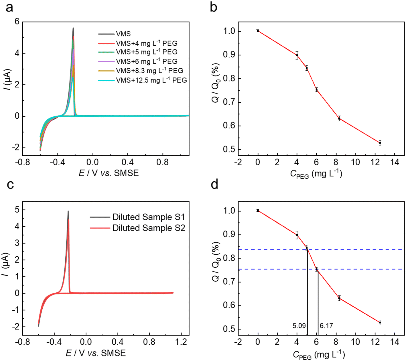 | ||
| Fig. 1 (a) Anodic stripping voltammograms obtained by the EMW in VMS (200 g L−1 CuSO4·5H2O + 40 g L−1 H2SO4 + 50 mg L−1 Cl−) with different PEG concentrations. (b) Calibration curve of the normalized stripping charge of Cu as a function of PEG concentration derived from the data in (a). (c) Anodic stripping voltammograms obtained in the diluted sample S1 and sample S2. (d) PEG concentration in diluted sample S1 and sample S2 determined from the calibration curve in (b). The potential was scanned from the OCP cathodically to −0.6 V, then anodically to 1.0 V, and back to the OCP with a scan rate of 50 mV s−1. | ||
To study the interferences of the accelerator and leveler on the detection of the suppressor concentration, we prepared two electroplating solution samples: one with different SPS concentrations (2.0, 2.5, 3.0, 3.5, and 4.0 mg L−1) prepared by adding accelerator to SPS-free solution (200 g L−1 CuSO4·5H2O + 40 g L−1 H2SO4 + 50 mg L−1 Cl− + 4 mg L−1 JGB + 500 mg L−1 PEG, defined as AFE), and the other with different JGB concentrations (3.0, 3.5, 4.0, 4.5 and 5.0 mg L−1) prepared by adding JGB to the leveler-free solution (200 g L−1 CuSO4·5H2O + 40 g L−1 H2SO4 + 50 mg L−1 Cl− + 3 mg L−1 SPS + 500 mg L−1 PEG, defined as LFE). The samples were injected and mixed with VMS in a volume ratio of 1:99 and tested using the EMW (Fig. 2a and c). As shown in Fig. 2a and b, the relative standard deviation (RSD) for samples with different SPS concentrations was calculated to be 0.79%. From Fig. 2c and d, the RSD for samples with different JGB concentrations was 1.04%. The results show that SPS and JGB interfere little with the detection of the PEG concentration.
 | ||
| Fig. 2 (a) Anodic stripping voltammograms obtained by the EMW in AFE (200 g L−1 CuSO4·5H2O + 40 g L−1 H2SO4 + 50 mg L−1 Cl− + 4 mg L−1 JGB + 500 mg L−1 PEG) with different SPS concentrations. (b) Anodic stripping charge of Cu as a function of SPS concentration. (c) Anodic stripping voltammograms obtained by the EMW in LFE (200 g L−1 CuSO4·5H2O + 40 g L−1 H2SO4 + 50 mg L−1 Cl− + 3 mg L−1 SPS + 500 mg L−1 PEG) with different JGB concentrations. (d) Anodic stripping charge of Cu as a function of JGB concentration. The insets in (a) and (c) display enlarged views detailing the voltammograms at −0.22 V. | ||
2.2 Detection of the concentration of the leveler JGB
Here, JGB was chosen as a testing leveler in the EMW. JGB has been demonstrated to be able to adsorb on the Cu surface and hinder Cu electrodeposition by cyclic voltammetry and surface-enhanced Raman spectroscopy.48 Theoretical calculations have revealed that the unsaturated molecular structure of JGB endows it with strong adsorption capability and high reaction activity compared to PEG and bis-(3-sulfopropyl)disulfide (MPS/SPS), suggesting unsaturated bonds as the molecular characteristics of a highly effective leveler.49 Furthermore, synergistic interactions between JGB and other bath components have been reported. JGB is considered to form a complex inhibitor with PEG and Cl−, which enhances the copper electrodeposition suppression effects.50 The principle of the leveler concentration detection is based on its ability to inhibit Cu2+ electroreduction. However, to exclude the interference of SPS on the concentration detection of JGB, we must determine the saturated concentration of SPS.The PEG-containing solution (VMS + 500 mg L−1 PEG) and a PEG–SPS containing solution with 100 mg L−1 SPS (VMS + 500 mg L−1 PEG + 100 mg L−1 SPS) were prepared and injected separately into the microfluidic chip, resulting in mixed solutions containing 0, 25, 50, 75 and 100 mg L−1 SPS. The mixed solutions were then studied in turn (Fig. 3a). As shown in Fig. 3b, the anodic stripping charge of Cu changed little when the SPS concentration exceeded 50 mg L−1. Thus, we adopted 75 mg L−1 as the saturated concentration of SPS when detecting the concentration of JGB.
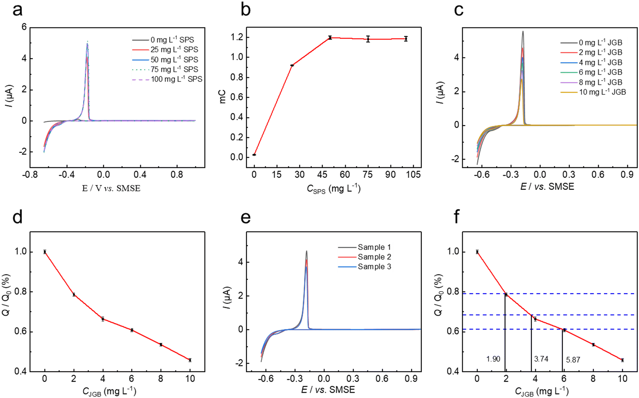 | ||
| Fig. 3 (a) Anodic stripping voltammograms obtained by the EMW in VMS with 500 mg L−1 PEG and different SPS concentrations. (b) Anodic stripping charge of Cu as a function of SPS concentration. (c) Anodic stripping voltammograms obtained by the EMW in VMS with 500 mg L−1 PEG, 75 mg L−1 SPS and different JGB concentrations. (d) Calibration curve of the anodic stripping charge of Cu as a function of JGB concentration. (e) Anodic stripping voltammograms obtained by the EMW for sample 1, sample 2 and sample 3. (f) JGB concentration detection of the three samples based on the data from (e) and the calibration curve in (d). | ||
The PEG–SPS standard solution (VMS + 500 mg L−1 PEG + 75 mg L−1 SPS) and the PEG–SPS–JGB standard solution (VMS + 500 mg L−1 PEG + 75 mg L−1 SPS + 20 ppm JGB) were prepared and injected into the microfluidic chip, where they were mixed with different volume ratios of 9:1, 8:2, 7:3, 6:4 and 5:5, in order to give the standard JGB concentrations and obtain the calibration curve. The targeted standard solutions containing 500 mg L−1 PEG, 75 mg L−1 SPS, and 2, 4, 6, 8, 10 mg L−1 JGB, were studied in turn (Fig. 3c), showing that JGB inhibited Cu2+ electrodeposition. The anodic stripping charges of Cu at the different JGB concentrations were obtained, and the calibration curve was plotted as shown in Fig. 3d. The normalized anodic stripping charge Q/Q0 decreased with increasing JGB concentration, where Q0 was obtained in the PEG–SPS standard solution.
The compositions of three practical electroplating solutions L1, L2 and L3 are listed in Table 1. To exclude the interference of SPS on the detection of the JGB concentration, we adjusted the concentration of JGB to 75 mg L−1 SPS and labeled the resulting solutions as sample 1, sample 2 and sample 3 (Table 1). Fig. 3e shows the stripping voltammograms obtained for the three samples, and Fig. 3f shows the corresponding concentrations of JGB obtained using the calibration curve in Fig. 3d. The controlled concentrations of JGB of the samples were 2 mg L−1, 4 mg L−1 and 6 mg L−1, indicating a mean relative error as low as 4.5%.
| Component | CuSO4·5H2O (g L−1) | H2SO4 (g L−1) | Cl− (mg L−1) | PEG (mg L−1) | SPS (mg L−1) | JGB (mg L−1) |
|---|---|---|---|---|---|---|
| Sample L1 | 200 | 40 | 50 | 500 | 3 | 2 |
| Sample L2 | 200 | 40 | 50 | 500 | 3 | 4 |
| Sample L3 | 200 | 40 | 50 | 500 | 3 | 6 |
| Sample 1 | 200 | 40 | 50 | 500 | 78 | 2 |
| Sample 2 | 200 | 40 | 50 | 500 | 78 | 4 |
| Sample 3 | 200 | 40 | 50 | 500 | 78 | 6 |
2.3 Detection of the concentration of the accelerator SPS
Here, we chose SPS as the accelerator. SPS has been demonstrated to be able to facilitate Cu2+ electrodeposition through synergistic interaction with Cl− anions; e.g., the electron paramagnetic resonance (EPR) spectroscopy results confirmed that SPS could not accelerate Cu2+ electrodeposition independently.51 The principle of detecting the concentration of SPS is based on its acceleration effect on Cu2+ electrodeposition.The standard samples (VMS + 500 mg L−1 PEG + 4 mg L−1 JGB + 0, 0.2, 0.4, 0.8 and 1.2 mg L−1 SPS) were prepared by mixing the standard solution A (VMS + 500 mg L−1 PEG + 4 mg L−1 JGB) and B (VMS + 500 mg L−1 PEG + 4 mg L−1 JGB + 1.2 mg L−1 SPS) in the microfluidic chip. The targeted samples containing 0, 0.2, 0.4, 0.8 and 1.2 mg L−1 SPS were studied in turn, as shown in Fig. 4a. The anodic stripping charges of Cu with different SPS concentrations were obtained, and the calibration curve was plotted as shown in Fig. 4b, demonstrating that SPS has a significant acceleration effect on Cu2+ electrodeposition, although the controlled SPS concentrations are much lower than those in practical acidic Cu electroplating solution.
 | ||
| Fig. 4 (a) Anodic stripping voltammograms obtained in VMS containing 500 mg L−1 PEG, 4 mg L−1 JGB and different SPS concentrations. (b) Calibration curve of the normalized anodic stripping charge of Cu as a function of SPS concentration. (c) Anodic stripping voltammograms of sample A1, sample A2 and sample A3. (d) SPS concentrations of the three samples derived from the calibration curve. | ||
The testing samples with different concentration of SPS are described and denoted as A1, A2 and A3 in Table 2. Since the SPS concentrations are outside the concentration range of the standard curve (Fig. 4b), the three samples were diluted 7.5-fold with standard solution A before the experiment. Fig. 4c presents the anodic stripping voltammograms, and Fig. 4d indicates the SPS concentrations derived from the calibration curve: 1.40 mg L−1, 2.79 mg L−1 and 4.31 mg L−1 for sample A1, A2 and A3 respectively, indicating a mean relative error of 5.7%.
| Component | CuSO4·5H2O (g L−1) | H2SO4 (g L−1) | Cl− (mg L−1) | PEG (mg L−1) | JGB (mg L−1) | SPS (mg L−1) |
|---|---|---|---|---|---|---|
| Sample A1 | 200 | 40 | 50 | 500 | 4 | 1.5 |
| Sample A2 | 200 | 40 | 50 | 500 | 4 | 3 |
| Sample A3 | 200 | 40 | 50 | 500 | 4 | 4.5 |
Moreover, we tested an industrial sample provided by Nantong Qunan Electronic Materials Co. Ltd., and the mean relative errors were 6.5% for the accelerator, 6.2% for the leveler and 3.6% for the suppressor, as detailed in ESI-1† and Fig. S1–S3. The results demonstrated the competitive capability of our EMW instrumental system.
3 Conclusions
An electrochemical microfluidic workstation (EMW) integrating a 3D printed microfluidic chip, a pumper injection system and a potentiostat was developed for the on-line detection and in-time supplementation of the suppressor, accelerator, and leveler in acidic Cu electroplating solutions. Employing the EMW, the mean relative error for the concentration detection of electroplating additives is much lower than 10%, which meets the requirements of industrial lab analysis. It should be noted that the solution volume consumed for each sample is only 220 μL, which will reduce not only the consumption of materials but also the solution preparation workload required in conventional CVS protocols. More importantly, the microfluidic system and the potentiostat can be easily miniaturized and integrated in a portable suitcase (ESI-2†), showing a prospective industrial application in the production line.4 Experimental section
4.1 Chemicals and instruments
CuSO4·5H2O, H2SO4 and HCl were purchased from Sinopharm Chemical Reagent Co., Shanghai, China. Janus Green B (JGB) was purchased from Yuanye Biotechnology Co., Shanghai, China. Polyethylene glycol (PEG) was purchased from Kaiwei Chemical Reagent Co., Shanghai, China. Bis-(sodium sulfopropyl)-disulfide (SPS) and 1H,1H,2H,2H-perfluorooctyltrichlorosilane (PFOCTS) were purchased from Aladdin Chemical Reagent Co., Shanghai, China. 2-(Difluoromethoxymethyl)-1,1,1,2,3,3,3-heptafluoropropane was purchased from Shanghai Ruiyi Environmental Protection Technology Co., Shanghai, China. Electronic fluorinated solution (Novec7100) was purchased from Shenzhen Zhongfluoride Technology Co., Shenzhen, China. All chemicals and reagents were of analytical or higher grade and were used without further purification. All the solutions were prepared with deionized water (18.2 MΩ cm, Milli-Q, Millipore Corp).A 3D printer was employed to fabricate the microfluidic chip mold (Halot-One Plus, Creality Technology Co., China). A program-controlled multichannel injection pump system was adopted to drive and mix the solutions in the microfluidic chip (TS-1B, Baoding Dichuang Electronic Technology Co., China). An oxygen plasma cleaner was used to modify the inner surface of the PDMS microfluidic chip (PDC-002-HP, Harrick Plasma Inc., USA). A scanning confocal laser microscope (SCLM, VKX1000, KEYENCE Co., Japan) was employed to characterize the surface roughness of the PDMS microfluidic chip. All the electrochemical experiments were performed with a CHI760e workstation (Shanghai Chenhua Co., China).
4.2 Fabrication of the PDMS microfluidic chip
A schematic diagram of the fabrication processes of the PDMS microfluidic chip is shown in Fig. 5a. Firstly, the mold of the microfluidic chip was designed using the software SolidWorks (SolidWorks, USA) and fabricated using the 3D printer. As shown in Fig. 5b, the microfluidic chip has dimensions of 91 mm (length) by 42 mm (width) by 13 mm (height). The microchannels featured a cross-section with a width of 400 μm and a height of 300 μm. The herringbone structure in the microchannels had a width of 100 μm and a height of 100 μm, and incorporated 90 degree bends. The spatial resolution of the 3D printer was 40 μm in the x–y axis and 50 μm in the z-axis, which was sufficient to ensure fabrication accuracy. As reported previously,52 the resin microstructure was printed layer-by-layer with a layer thickness of 50 μm and z-axial printing rate of 2 cm h−1, and each layer was photo-cured by UV light for 3.5 seconds. Once the 3D printing was completed, the obtained mold was rinsed with ethanol several times to remove the unreacted resin. After air-drying, the mold was photo-cured using UV light for another 600 seconds to strengthen the microstructures and improve the durability.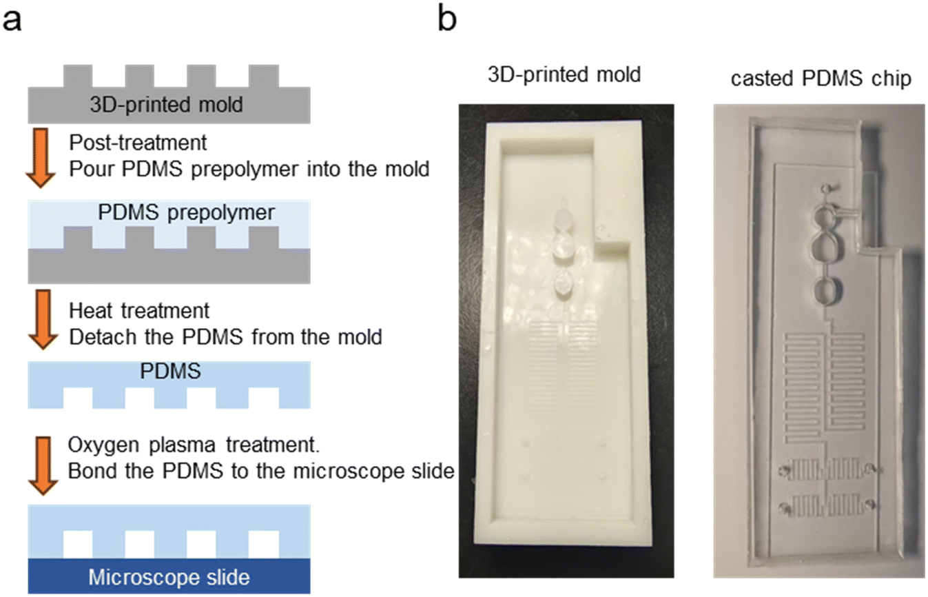 | ||
| Fig. 5 (a) Schematic diagram of the fabrication processes of the PDMS microfluidic chip. (b) Images of the 3D-printed mold and the casted PDMS chip. | ||
Secondly, PDMS was casted on the mold to transfer the microstructures. To ensure conformality, the 3D-printed mold was heated at 80 °C for 8 h to remove the residual monomers and catalysts in the resin, which may inhibit the polymerization of PDMS.53,54 To ensure the demold quality, the mold surface was silylated in a mixed solution containing 20 μL PFOCTS and 1 mL Novec7100. The obtained PDMS chip was rinsed with anhydrous ethanol for 5 minutes and heated for another 4 h at 80 °C. From the confocal laser scanning microscopy (CLSM) image shown in Fig. S5,† the arithmetic mean height (Sa) and maximum height (Sz) parameters were measured to be 0.093 μm and 1.666 μm, indicating that the detached PDMS surface was smooth enough for usage as a microfluidic chip.
Thirdly, the obtained PDMS was treated with a Harrick Plasma cleaner for surface functionalization with a power of 30 watts for 5 minutes in an oxygen-rich atmosphere, which is important to enhance the bonding intensity of the PDMS chip on the glass slide. The PDMS chip was attached to a glass slide cleaned by piranha solution (volume ratio of concentrated H2SO4 to H2O2: 7:3), and the microfluidic chip was then prepared and ready for use.
4.3 Configuration of the electrochemical microfluidic workstation (EMW)
As shown in Fig. 6, the EMW includes three modules: a microfluidic chip, a pumper injection system and a potentiostat. The program-controlled pumper injection system injected the solutions into the microfluidic chip from the inlets, where they mixed in the mixing runner area and then entered the electrochemical micro-cell. A Pt UME (Fig. S6†), a 3-mm diameter Pt disc electrode and a saturated Hg/Hg2SO4 electrode (SMSE) were implanted in the electrochemical micro-cell as the working electrode, counter electrode and reference electrode for the electroanalytical detections. Because the flux in each inlet is set up automatically by the programed injection pumper controller, the target concentration of each additive in the mixed solution can be well controlled as expected. For each sample, the required volume of the solution was 220 μL, which will reduce the workload and materials compared with conventional CVS protocols. The microfluidic chip is very easily cleaned using deionized water and can be reused conveniently. As in the CVS protocols, anodic stripping voltammetry was adopted to calibrate and detect the additive concentrations. To check the feasibility of the EMW, control experiments were performed using both the EMW and a conventional CVS workstation. The testing solution used in CVS contained 150 g L−1 CuSO4·5H2O, 50 g L−1 H2SO4 and 50 mg L−1 Cl−. The same target solution in EMW was mixed in the microfluidic channels by injecting three mother solutions. As shown in Fig. S7,† the anodic stripping charge of the electrodeposited Cu was almost the same, demonstrating the qualified solution mixing performance of the microfluidic chip. | ||
| Fig. 6 Schematic diagrams of the (a) microfluidic chip, (b) electrochemical micro-cell, and (c) electrochemical microfluidic workstation. | ||
Data availability
This study adheres to principles of research transparency and reproducibility. All empirical data presented herein were generated through original experimental work conducted exclusively by the research team. The investigation did not employ pre-existing datasets, access restricted repositories, or analyze proprietary information beyond the results explicitly reported in this manuscript.Primary experimental data, including quantitative measurements, observational records, and analytical outputs, have been systematically embedded within the manuscript's graphical elements (figures) and tabular presentations (tables). A comprehensive description of experimental protocols, instrumentation specifications, and procedural parameters is provided in the experimental section, enabling independent verification of findings through experimental replication.
The authors confirm that:
(1) No supplementary datasets or external data deposits were created during this investigation.
(2) All essential methodological details required for result reproduction are fully documented in the main text.
(3) Data visualization techniques maintain scientific integrity without selective representation.
Researchers seeking to validate conclusions may reconstruct the complete dataset by implementing the described experimental workflow under equivalent laboratory conditions.
Conflicts of interest
The authors declare no conflict of interest.Acknowledgements
The authors are all thankful for the financial supports from the National Natural Science Foundation of China (22132003, 22202166) and National Key Research and Development Program of China (2023YFF0713900).References
- Y. Zhao, Z. Y. Wang, L. Jin, J. Q. Yang, T. Song, F. Z. Yang and D. P. Zhan, 1-Dodecyl-2-methyl-3-benzylimidazolium chloride as a novel leveler: Towards simultaneously both the microvia void-free filling and through hole conformal thickening, Colloids Surf., A, 2024, 695, 134239 CrossRef CAS.
- L. Jin, W. Q. Li, Z. Y. Wang, J. Q. Yang, A. N. Zheng, F. Z. Yang, D. P. Zhan, D. Y. Wu and Z. Q. Tian, Novel, simple, and green citrate-based copper electronic electroplating bath in microvia void-free filling for printed circuit board application, ACS Sustainable Chem. Eng., 2022, 10, 14204–14211 CrossRef CAS.
- Z. Y. Wang, L. Jin, G. Li, J. Q. Yang, W. Q. Li, D. P. Zhan, Y. X. Jiang, F. Z. Yang and S. G. Sun, Electrochemical and in situ FTIR spectroscopic studies of gentian violet as a novel leveler in through-holes metallization for printed circuit board applications, Electrochim. Acta, 2022, 410, 140018 CrossRef CAS.
- Y. N. Tao, C. Liang, Z. Q. Mei, Z. Q. Song, Y. Wu, Y. N. Sun, W. Q. Zhang, Y. Ruan and X. G. Zhao, Numerical simulation of copper electrodeposition for Through Silicon Via (TSV) with SPS-PEG-Cl additive system, Microelectron. J., 2024, 144, 106089 CrossRef CAS.
- F. L. Wang and Y. P. Le, Experiment and simulation of single inhibitor SH110 for void-free TSV copper filling, Sci. Rep., 2021, 11, 12108 CrossRef CAS PubMed.
- H. Kim, H. Jeon, D. J. Lee and J. Y. Kim, Surface residual stress in amorphous SiO2 insulating layer on Si substrate near a Cu through-silicon via (TSV) investigated by nanoindentation, Mater. Sci. Semicond. Process., 2021, 135, 106153 CrossRef CAS.
- T. Fritzsch, F. Huegging, P. Mackowiak, K. Zoschke, M. Rothermund, N. Owtscharenko, D. L. Pohl, H. Oppermann and N. Wermes, 3D TSV hybrid pixel detector modules with ATLAS FE-I4 readout electronic chip, J. Instrum., 2022, 17, C01029 CrossRef.
- W. S. Lv, J. X. Liu, X. Lei and F. L. Zhu, Role of Cu/SiO rough interface in TSV for high-power device under electromigration, IEEE Trans. Electron Devices, 2023, 70, 5281–5287 CAS.
- J. T. Wang, F. C. Duan, Z. W. Lv, S. Chen, X. F. Yang, H. T. Chen and J. H. Liu, A short review of through-silicon via (TSV) interconnects: metrology and analysis, Appl. Sci., 2023, 13, 8301 CrossRef CAS.
- P. Xu, H. Huang, B. Q. Zhang and Z. H. Tang, Thermal performance analysis of carbon materials based TSV in three dimensional integrated circuits, IEEE Access, 2023, 11, 75285–75294 Search PubMed.
- M. Zhang, F. Qin, S. Chen, Y. W. Dai, P. Chen and T. An, Protrusion of through-silicon-via (TSV) copper with double annealing processes, J. Electron. Mater., 2022, 51, 2433–2449 CrossRef CAS.
- G. Krause, D. Hofmann, B. Habets, S. Buhl, M. Gutsch, A. Lopez-Gomez, W. S. Kim and X. Thrun, Metrology, inspection, and process control for microlithography XXXII, SPIE, 2018 Search PubMed.
- K. Kinoshita, M. Tada, M. Hiroi, K. Shiba, T. Onodera, M. Tagami, S. Saitoh, Y. Hayashi, T. Usami and T. Kikkawa, Via-shape-control for copper dual-damascene interconnects with low-k organic film, IEEE Trans. Semicond. Manuf., 2008, 21, 256–262 Search PubMed.
- D. T. Price, R. J. Gutmann and S. P. Murarka, Damascene copper interconnects with polymer ILDs, Thin Solid Films, 1997, 308–309, 523–528 CrossRef CAS.
- S. Choe, M. J. Kim, H. C. Kim, T. Lim, K. J. Park, K. H. Kim, S. H. Ahn, A. Lee, S. K. Kim and J. J. Kim, Degradation of poly(ethylene glycol-propylene glycol) copolymer and its influences on copper electrodeposition, J. Electroanal. Chem., 2014, 714, 85–91 CrossRef.
- M. Ostra, C. Ubide and M. Vidal, Quantitative nuclear magnetic resonance for additives determination in an electrolytic nickel bath, Anal. Bioanal. Chem., 2011, 399, 1907–1915 CrossRef CAS PubMed.
- A. Barriola, J. I. Miranda, M. Ostra and C. Ubide, Determination of additives in an electrolytic zinc bath by q H-NMR spectroscopy, Anal. Bioanal. Chem., 2010, 398, 1085–1094 CrossRef CAS PubMed.
- S. Choe, M. J. Kim, H. C. Kim, S. K. Cho, S. H. Ahn, S. K. Kim and J. J. Kim, Degradation of bis(3-sulfopropyl) disulfide and its influence on copper electrodeposition for feature filling, J. Electrochem. Soc., 2013, 160, D3179–D3185 CrossRef CAS.
- A. Barriola, E. Garcia, M. Ostra and C. Ubide, Additive determination in an electrolytic zinc bath by UV-Visible spectroscopy and multivariate calibration, J. Electrochem. Soc., 2008, 155, D480–D484 CrossRef CAS.
- S. K. Kim and J. J. Kim, Superfilling evolution in Cu electrodeposition: Dependence on the aging time of the accelerator, Electrochem. Solid-State Lett., 2004, 7, C98–C100 CrossRef CAS.
- W. Wang, Y. B. Li and Y. L. Li, Invalidating mechanism of bis (3-sulfopropyl) disulfide (SPS) during copper via-filling process, Appl. Surf. Sci., 2009, 255, 4389–4392 CrossRef CAS.
- C. C. Hung, W. H. Lee, S. Y. Hu, S. C. Chang, K. W. Chen and Y. L. Wang, Effect of bis-(3-sodiumsulfopropyl disulfide) byproducts on copper defects after chemical mechanical polishing, J. Vac. Sci. Technol., B, 2008, 26, 255–259 CrossRef CAS.
- W. H. Lee, C. C. Hung, S. C. Chang and Y. L. Wang, Bis-(3-sodiumsulfopropyl disulfide) decomposition with cathodic current flowing in a copper-electroplating bath, J. Electrochem. Soc., 2010, 157, H131–H135 CrossRef CAS.
- L. D'Urzo, H. H. Wang, C. Tang, A. Pa and C. Zhi, Solid phase extraction-high-performance liquid chromatography detection of organic additives in acidic copper baths - II. Polyethylene-glycol based suppressors, J. Electrochem. Soc., 2005, 152, C697–C700 CrossRef.
- L. D'Urzo, H. H. Wang, A. Pa and C. Zhi, SPE-HPLC detection of organic additives in acidic copper plating baths - I. sulfopropyl disulfide-based brighteners, J. Electrochem. Soc., 2005, 152, C243–C247 CrossRef.
- S. Choe, M. J. Kim, K. H. Kim, H. C. Kim, J. C. Song, S. K. Kim and J. J. Kim, Accuracy improvement in cyclic voltammetry stripping analysis of thiourea concentration in copper plating baths, J. Electrochem. Soc., 2015, 162, H294–H300 CrossRef CAS.
- Z.-W. Sun, N. Kovarsky, C. Yu and G. Dixit, US Pat., US6773569, 2004 Search PubMed.
- G. Chalyt, P. Bratin, M. Pavlov, A. Kogan and M. J. Perpich, US Pat., US6572753, 2003 Search PubMed.
- S. Yaofeng, M. Gao and H. Xia, US Pat., US9575032, 2014 Search PubMed.
- M. Pavlov, E. Shalyt, P. Bratin and I. Tsimberg, US Pat., US8535504, 2013 Search PubMed.
- N. Nakayama, US Pat., US 9964518, 2018 Search PubMed.
- D. Tench and C. Ogden, A new voltammetric stripping method applied to the determination of the brightener concentration in copper pyrophosphate plating baths, J. Electrochem. Soc., 2019, 125, 194–198 CrossRef.
- S. J. Wu, D. W. Pan, Z. Y. Yu, Q. Kang and D. Z. Shen, Gold microelectrode arrays based electrode for determination of trace copper in seawater, Asian J. Chem., 2014, 26, 2741–2744 CrossRef CAS.
- F. H. Narouei, D. Andreescu and S. Andreescu, Rapid characterization of arsenic adsorption on single magnetite nanoparticles by collisions at microelectrodes, Environ. Sci.:Nano, 2020, 7, 1999–2009 RSC.
- Y. Z. Wang, R. Y. Xu, L. W. Chen, C. B. Wu, L. L. Qiu, C. D. Windle, Q. Han and L. T. Qu, Hierarchical ZnO@hybrid carbon core-shell nanowire array on a graphene fiber microelectrode for ultrasensitive detection of 2,4,6-trinitrotoluene, ACS Appl. Mater. Interfaces, 2020, 12, 8547–8554 CrossRef CAS PubMed.
- B. G. Xie, J. J. Sun, X. B. Chen, J. H. Chen, T. L. Xiang and G. N. Chen, In situ monitoring of additives in copper plating baths by cyclic voltammetric stripping with a microelectrode, J. Electrochem. Soc., 2007, 154, D516–D519 CrossRef CAS.
- G. Gonzalez, I. Roppolo, C. F. Pirri and A. Chiappone, Current and emerging trends in polymeric 3D printed microfluidic devices, Addit. Manuf., 2022, 55, 102867 CAS.
- A. G. Niculescu, C. Chircov, A. C. Bîrca and A. M. Grumezescu, Fabrication and applications of microfluidic devices: A review, Int. J. Mol. Sci., 2011, 2021, 22 Search PubMed.
- G. K. Liu, S. Z. Zou, D. Josell, L. J. Richter and T. P. Moffat, SEIRAS study of chloride-mediated polyether adsorption on Cu, J. Phys. Chem. C, 2018, 122, 21933–21951 CrossRef CAS.
- Z. V. Feng, X. Li and A. A. Gewirth, Inhibition due to the interaction of polyethylene glycol, chloride, and copper in plating baths: a surface-enhanced Raman study, J. Phys. Chem. B, 2003, 107, 9415–9423 CrossRef CAS.
- C. Wang, J. Q. Zhang, P. X. Yang and M. Z. An, Electrochemical behaviors of Janus Green B in through-hole copper electroplating: An insight by experiment and density functional theory calculation using Safranine T as a comparison, Electrochim. Acta, 2013, 92, 356–364 CrossRef CAS.
- W. P. Dow, C. C. Li, Y. C. Su, S. P. Shen, C. C. Huang, C. Lee, B. Hsu and S. Hsu, Microvia filling by copper electroplating using diazine black as a leveler, Electrochim. Acta, 2009, 54, 5894–5901 CrossRef CAS.
- L. Jin, Z. Y. Wang, Z. Y. Cai, J. Q. Yang, A. N. Zheng, F. Z. Yang, D. Y. Wu and D. P. Zhan, 1-(2-Pyridylazo)-2-naphthol as a synergistic additive for improving throwing power of through hole copper electronic electroplating, J. Ind. Eng. Chem., 2023, 125, 269–276 CrossRef CAS.
- L. Jin, A. N. Zheng, M. Wang, J. Q. Yang, Z. Y. Wang, F. Z. Yang, D. Y. Wu and D. P. Zhan, Insights into the synergistic effects of safranine in an acidic copper bath on through-hole void-free filling for high-quality electronics interconnection, Colloids Surf., A, 2023, 671 CAS.
- J. Li, G. Y. Zhou, Y. Hong, C. Wang, W. He, S. X. Wang, Y. M. Chen, Z. S. Wen and Q. Y. Wang, Copolymer of pyrrole and 1,4-butanediol diglycidyl as an efficient additive leveler for through-hole copper electroplating, ACS Omega, 2020, 5, 4868–4874 CrossRef CAS PubMed.
- L. Zheng, W. He, K. Zhu, C. Wang, S. X. Wang, Y. Hong, Y. M. Chen, G. Y. Zhou, H. Miao and J. Q. Zhou, Investigation of poly (1-vinyl imidazole 1, 4-butanediol diglycidyl ether) as a leveler for copper electroplating of through-hole, Electrochim. Acta, 2018, 283, 560–567 CrossRef CAS.
- M. X. Tang, S. T. Zhang, Y. J. Qiang, S. J. Chen, L. Luo, J. Y. Gao, L. Feng and Z. J. Qin, 4,6-Dimethyl-2-mercaptopyrimidine as a potential leveler for microvia filling with electroplating copper, RSC Adv., 2017, 7, 40342–40353 RSC.
- B. Bozzini, L. D'Urzo, C. Mele and V. Romanello, Electrodeposition of Cu from acidic sulphate solutions in the presence of polyethylene glycol and chloride ions, J. Mater. Sci.:Mater. Electron., 2006, 17, 915–923 CrossRef CAS.
- Z. Q. Lai, S. X. Wang, C. Wang, Y. Hong, G. Y. Zhou, Y. M. Chen, W. He, Y. Q. Peng and D. J. Xiao, A comparison of typical additives for copper electroplating based on theoretical computation, Comput. Mater. Sci., 2018, 147, 95–102 CrossRef CAS.
- W. P. Dow, H. S. Huang, M. Y. Yen and H. C. Huang, Influence of convection-dependent adsorption of additives on microvia filling by copper electroplating, J. Electrochem. Soc., 2005, 152, C425–C434 CrossRef CAS.
- W. P. Dow, H. S. Huang, M. Y. Yen and H. H. Chen, Roles of chloride ion in microvia filling by copper electrodeposition - II. studies using EPR and galvanostatic measurements, J. Electrochem. Soc., 2005, 152, C77–C88 CrossRef CAS.
- A. I. Shallan, P. Smejkal, M. Corban, R. M. Guijt and M. C. Breadmore, Cost-effective three-dimensional printing of visibly transparent microchips within minutes, Anal. Chem., 2014, 86, 3124–3130 CrossRef CAS PubMed.
- G. Comina, A. Suska and D. Filippini, PDMS lab-on-a-chip fabrication using 3D printed templates, Lab Chip, 2014, 14, 424–430 RSC.
- H. N. Chan, Y. F. Chen, Y. W. Shu, Y. Chen, Q. Tian and H. K. Wu, Direct, one-step molding of 3D-printed structures for convenient fabrication of truly 3D PDMS microfluidic chips, Microfluid. Nanofluid., 2015, 19, 9–18 CrossRef CAS.
Footnote |
| † Electronic supplementary information (ESI) available. See DOI: https://doi.org/10.1039/d5im00073d |
| This journal is © Institute of Process Engineering of CAS 2025 |