Lithographic performances of aryl sulfonate ester-modified polystyrenes as nonchemically amplified resists†
Received
2nd April 2025
, Accepted 30th May 2025
First published on 12th June 2025
Abstract
Aryl sulfonate ester modified polystyrenes with different substituents (X–SEPS, X = H–, MeO–, and CN–) were synthesized by reversible addition-fragmentation chain transfer (RAFT) polymerization. The excellent thermal stability and film-forming capability of these three polymers suggest that they can satisfy the lithography process and are candidates for resist materials. Comparative electron beam lithography (EBL) demonstrates that the three resists (H–SEPS, MeO–SEPS and CN–SEPS) exhibit different EBL performances. Calculation of bond energies for the model compounds suggests that the influence of substituent groups on the bond energy is not the reason for the differences in sensitivity. Results obtained using a fully automated dissipative quartz crystal microbalance (QCM) analyzer confirm that the influence of substituent groups on the solubility behavior of resist films in developers leads to different photolithographic performances. The H–SEPS resist exhibits better comprehensive performance than the MeO–SEPS and CN–SEPS resists, achieving an 18 nm line/space (L/S) pattern and a 10 nm line/4 space (L/4S) semi-dense pattern by EBL at doses of 3200 and 2800 μC cm−2, respectively. Further extreme ultraviolet lithography (EUVL) demonstrates the capability of H–SEPS resist to form 22 nm half-pitch (HP) patterns. The detailed study of the photochemical reaction and patterning mechanism suggests that the decomposition of sulfonate ester groups into polar sulfonic acid groups, along with a rearrangement, leads to a solubility switch of resist films in the developer.
Keywords: Nonchemically amplified resist; Reversible addition-fragmentation chain transfer polymerization; Aryl sulfonate; Electron beam lithography; Extreme ultraviolet lithography.
1 Introduction
Photolithography is the cornerstone of the modern semiconductor industry, driving significant advances in integrated circuit (IC) manufacturing and information technology.1 In recent decades, ongoing innovations in photolithography have facilitated the reduction of the feature size of semiconductor devices from several micrometers to below 20 nm.2,3 The essence of photolithography lies in the exposure process, which forms nanopatterns in the resist layer and then transfers the pattern onto the substrate by etching. Consequently, resist materials have become one of the urgent factors,4 and the development of high-performance resist materials with high resolution (R), sensitivity (S), low line edge roughness (LER) or line width roughness (LWR) is an important issue in advanced photolithography.5–7
Nonchemically amplified resists (n-CARs) have received increasing attention in recent years due to its potential to achieve high-resolution and low LER patterns.2,6,8–15 Different from chemically amplified resists (CARs), which rely on acid diffusion and chemical amplification to increase sensitivity, n-CARs are usually single-component, avoiding uneven component distribution and uncontrollable reaction kinetics.6 In n-CARs, the photosensitive group incorporated into the main skeleton or side chains undergoes direct photochemical reactions upon irradiation, resulting in chain scission, cross-linking, or polarity change, which facilitates the solubility conversion of resist film in developers.6 A prominent example of n-CARs is the chain-scission polymethyl methacrylate (PMMA) resist, which achieves a 16 nm dense line/space (L/S) pattern with an LER of 2.2 nm at a dose of 110 mJ cm−2 in extreme ultraviolet lithography (EUVL).16 Gonsalves's group reported a series of negative-tone n-CARs based on copolymers bearing radiation-sensitive sulfonium functionality in recent years,14,17–20 one of which achieved sub-15 nm L/S patterns with low LERs using electron beam lithography (EBL).19 Our research group has developed several novel polymeric resists based on oxime ester groups,21,22 which demonstrated significantly improved sensitivity and resolution, achieving feature sizes down to 18 nm.
Sulfonate esters are rarely studied as photosensitive groups in previous reports on n-CARs.23 Sulfonate ester compounds are usually used as non-ionic photoacid generators (PAGs) in CAR formulations for both ultraviolet (UV) and EBL.24 During the exposure process, the sulfonate ester group decomposes, yielding the corresponding sulfonic acids and phenolic compounds. Then, sulfonic acid catalyzes the decomposition or polymerization of acid-sensitive resist material.25–27 Inspired by the photosensitivity of the sulfonate ester group and the polarity difference before and after exposure, we consider it possible to design a new type of n-CARs based on sulfonate ester.
Herein, a series of aryl sulfonate ester-modified polystyrene derivatives with different substituents (X–SEPS, X = H–, MeO–, and CN–) were designed and synthesized, as shown in Fig. 1. The change in substituent groups affects the solubility of the resist materials in the developer and changes the elemental composition of the materials, thus affecting the sensitivity, resolution and LER of the resist patterns. An aryl ester group was introduced into the side chain to increase the resistance of the resist film, which is an important parameter for pattern transfer by etching.28 The polydispersity and molecular weight of polymers also affect the pattern resolution and LER formed by the resist material.7 To improve the resolution and reduce LER, the polystyrene derivatives were synthesized by the reversible addition-fragmentation chain transfer (RAFT) polymerization, giving the polydispersity index (PDI) below 1.2 and the molecular weight (Mw) between 5.7 and 7.1 kDa for the polymers. The n-CAR based on the polymers was extensively evaluated by EBL and EUV lithography, achieving 18 nm L/S and 10 nm L/4S lithographic patterns with low LERs, respectively. The exposure mechanism was further investigated, confirming that the decomposition of sulfonate ester during exposure causes a solubility switch.
 |
| | Fig. 1 Structures of aryl sulfonate ester-modified polystyrenes with hydrogen, methoxyl, and cyanide substituents (X–SEPS, X = H–, MeO–, and CN–). | |
2 Results and discussion
2.1 Synthesis and characterization of aryl sulfonate ester-modified polystyrene (X–SEPS)
The procedure for the synthesis of the aryl sulfonate ester polymers is shown in Scheme 1. Treatment of sodium 4-styrene sulfonate with dichlorosulfoxide in N,N-dimethylformamide (DMF) quantitatively yields 4-styrene sulfonyl chloride. The etherification of 4-styrene sulfonyl chloride with para-substituted phenol afforded aryl 4-styrene sulfonate ester monomers. Further polymerization of the monomers by RAFT in the presence of the chain transfer agent isopropyl dithiobenzoate (CDB) and free radical initiator 2,2′-azobis(2-methylpropionitrile) (AIBN) gave the aryl sulfonate ester-modified polystyrene with the target Mw and PDI. The experimental procedures are detailed in the ESI.† The synthesized monomers were fully characterized using 1H NMR, HR-MS, and FTIR spectroscopy (Fig. S1–S7†), confirming the successful preparation of the monomers. The aryl sulfonate ester-modified polystyrene was further characterized by 1H NMR (Fig. S8–S10†) and GPC, yielding Mw values between 5.7 and 7.1 kDa and PDI values below 1.2, respectively (Fig. S11,†Table 1).
 |
| | Scheme 1 Synthetic procedure for aryl sulfonate ester-modified polystyrene (X–SEPS). | |
Table 1 Characterization and physical properties of the aryl sulfonate ester-modified polystyrene
| Polymer |
Mn |
Mw |
PDI |
T
d (°C) |
T
g (°C) |
RMS (nm) |
| H–SEPS |
6.2 kDa |
6.5 kDa |
1.05 |
375 |
101 |
0.31 |
| MeO–SEPS |
6.7 kDa |
7.1 kDa |
1.05 |
321 |
90 |
0.30 |
| CN–SEPS |
5.3 kDa |
6.0 kDa |
1.14 |
281 |
108 |
0.30 |
2.2 Physical properties of the X–SEPS
Good thermal stability and film-forming properties are prerequisites for resist materials. The thermogravimetric analysis (TGA) of all the polymers was conducted using a comprehensive thermal analyzer, and the decomposition temperature (Td) of the polymers was above 200 °C (Fig. S12a†). Differential scanning calorimetry (DSC) revealed that the glass-transition temperatures (Tg) of the polymers were in the range of 90–108 °C (Fig. S12b†). The side-chain substituent is significantly efficient at the Tg of polymers. CN–SEPS exhibits the highest Tg of 108 °C among the polymers, while MeO–SEPS exhibits the lowest Tg of 90 °C. The increased Tg of the CN–SEPS may be attributed to the increased polarity of sidechains by the CN group, which improves the interaction between the polymer chains.29,30 The results demonstrate the excellent thermal stability of the polymers, which are stable enough for the baking process in lithography. To demonstrate the film-forming ability of the polymers, the surface morphology of the spin-coated films was investigated by AFM (Fig. S12c†). The root-mean-square (RMS) roughness of the polymer films was calculated to be about 0.29–0.31 nm in an area of 5 × 5 μm2 (Table 1). These results indicate that the polymer films are sufficiently smooth to meet the requirements of high-resolution lithography.
2.3 Primary optimization of the developers for X–SEPS resists
As n-CARs, post-exposure baking (PEB) is not a necessary process because it avoids the subsequent chemical amplification.20 In this case, the development process is a key factor in lithography. To investigate the developers of the X–SEPS resists, 254 nm light (∼10 mW cm−2) was used to expose the spin-coated resist films for 4 min. The thickness of the resist films before and after development by different developers was then measured using an ellipsometer. The film remaining ratio was calculated by comparing the film thicknesses. In the case of positive tone development (PTD), the film remaining ratio for the exposed area should be low (close to 0%), whereas the unexposed area exhibits a high remaining ratio. Conversely, the developer dissolves the unexposed area as much as possible to increase the residual film rate in the exposed area with negative-tone development (NTD). After exposure to 254 nm, the remaining ratios of the polymer resist films before and after development in different developers are shown in Table S1.† Nine different developers were investigated. Developers such as butyl acetate, ethanol, isopropanol, n-propanol, and TMAH cannot fulfill the requirements of all three polymer resists. The results show that methyl isobutyl ketone (MIBK), acetonitrile (AN), and 1,2-dichloroethane can be used as the common developers of these three polymer resists, all providing NTD patterns. Considering that MIBK is more commonly used in the semiconductor industry and the film remaining ratio of the three polymer resist films is high in MIBK, we used MIBK as a common developer to evaluate the photolithographic performance of the polymer resists. The use of MIBK as a developer for X–SEPS resists was further confirmed by 254 nm lithography. As shown in Fig. S13,† all three polymeric resists can form uniform micron-scale NTD patterns, indicating the solubility switching and patterning ability of X–SEPS resists in MIBK developers.
2.4 EBL performance of the X–SEPS resists
The lithographic performance of the X–SEPS resists in the MIBK developer was further investigated by EBL. The dose-to-gel curve was used to analyze the contrast and sensitivity of the three polymer resists. A series of frames of 1.5 × 1.5 μm2 were exposed on the resist films with increasing doses, starting at 65 μC cm−2 with a dose increment of 15%. After exposure, the wafers with resists were developed in MIBK for 60 s and dried under nitrogen flow. The thickness of the exposed frames was measured by AFM. A three-dimensional (3D) AFM image of the H–SEPS patterns is shown in Fig. 2a as an example. With increasing exposure dose, the film thickness gradually increases and finally reaches an almost constant thickness, showing an NTD resist characteristic. The contrast curves were obtained from the AFM images by measuring the variation in retained film thickness with dose, as shown in Fig. 2b (black). The other X–SEPS resists exhibited similar NTD characteristics. A logistic function was used to fit the data,31,32 and a slope at y = 0.5 was created to form a line. The doses of the line at y = 0 and y = 1 are denoted as D0 and D100, respectively. The D100 is used to evaluate the sensitivity of the resist, and the contrast value (γ) was calculated by formula (1).33| |  | (1) |
 |
| | Fig. 2 (a) 3D AFM images of the H–SEPS resist pattern at different exposure doses after development in MIBK. (b) Contrast curves of X–SEPS resists. | |
The calculated EBL sensitivity and contrast of the three X–SEPS resists are summarized in Table 2. The CN–SEPS resist exhibits the highest sensitivity (1196 μC cm−2) but poor contrast (1.4). The contrasts of the H–SEPS and MeO–SEPS resists are both above 3, suggesting the potential to form high-resolution patterns. The sensitivities of the three resists were in the order of SCN–SEPS (1196 μC cm−2) > SH–SEPS (2264 μC cm−2) > RMeO–SEPS (3276 μC cm−2), and the contrasts were in the order of γH–SEPS (4.1) > γMeO–SEPS (3.2) > γCN–SEPS (1.4). The results suggest that the different substituents of the aryl sulfonate ester-modified polystyrene exhibited a significant effect on the lithographic performance of the resists.
Table 2 Sensitivity and contrast of X–SEPS resists developed by EBL in MIBK
| Resist |
Sensitivity (D100, μC cm−2) |
Contrast |
| H–SEPS |
2264 |
4.1 |
| MeO–SEPS |
3276 |
3.2 |
| CN–SEPS |
1196 |
1.4 |
To confirm the patterning capability, the lithographic performance of the X–SEPS resists was further investigated by EBL. Fig. 3 shows SEM images of 30, 25, 22 and 20 nm half-pitch (HP) line/space (L/S) patterns together with their LERs and LWRs for the three resist materials. All the resists were patterned under the same lithographic process conditions, that is, the film thickness of 30 nm and MIBK developer for 60 s. The H–SEPS and MeO–SEPS resists can resolve the 30, 25 and 22 nm HP patterns without collapse or bridge defects at exposure doses of 3400 and 4600 μC cm−2, respectively. However, in the case of a smaller feature size of 20 nm, the patterns became blurred because of the collapse due to the high aspect ratio, suggesting the limitation of the resolution of 20 nm for X–SEPS resists during the lithographic process. The CN–SEPS resist failed to give any clear lithographic patterns even at the best exposure dose of 2500 μC cm−2, maybe due to its low contrast. The LER and LWR of the SEM images of the lithographic pattern were calculated by the software ProSEM (Fig. S15–S20†). The LER and LWR values of the 22 nm HP patterns formed by the H–SEPS resists are only 2.6 and 4.3 nm, respectively, which are smaller than those of the chemically amplified photoresist.6,12 These results confirm the ability of the H–SEPS and MeO–SEPS resists to form high-resolution patterns.
 |
| | Fig. 3 SEM images of 30, 25, 22 and 20 nm HP line/space patterns formed by aryl sulfonate ester-modified polymer resists using EBL. (a) H–SEPS and MeO–SEPS resist patterns. (b) CN–SEPS resist patterns (developer: MIBK; film thickness: ∼30 nm). | |
The three (H–SEPS, MeO–SEPS and CN–SEPS) resists exhibit different EBL performances. The H–SEPS resist exhibits higher sensitivity, contrast, and lower LER and LWR values for patterning, suggesting excellent comprehensive performance among the three resists. The MeO–SEPS resist exhibits the poorest sensitivity and LER. The CN–SEPS resist is the most sensitive, but its contrast is too low to provide clear patterns. The lithographic conditions were almost the same for the three resists except for the substituents of the aryl sulfonate ester structure. The difference in patterning performance is attributed to the presence of substituents of H, MeO–, and CN– groups in the aryl sulfonate ester-modified polystyrenes.
A previous report demonstrated that the homolytic cleavage of ArO–S bonds in aryl sulfonate ester groups occurs after exposure,34 resulting in the formation of sulfonic acid and phenolic compounds (see the following mechanism study). The effect of substituents on the ArO–S bond energy of the aryl sulfonate ester may be an important factor leading to the difference in sensitivity.22 Smaller bond energy will lead to facile cleavage and higher sensitivity of the corresponding resist. To understand the differences among these resists for patterning, the bond energy (or dissociation energy) of the ArO–S bonds in the three model compounds (Fig. S14†) of aryl ester sulfonates was calculated using the ORCA 5.0.3 software package based on density functional theory (ESI†). The bond energies of ArO–S bonds (Ebond) were calculated to be 291.5, 278.8, and 294.8 kJ mol−1 for the hydrogen (H–), methoxy (CH3O–), and cyano (CN–) groups substituted model compounds, respectively (Table S2†). It was found that the substituents of aryl sulfonate ester result in different bond energies. However, the bond energy is not consistent with the sensitivity of the corresponding resists. The hydrogen- and cyano-substituted model compounds exhibited higher bond energy than that of the methoxy-substituted model compound, whereas the corresponding substituted polymeric resists showed higher sensitivity. This suggests that the influence of the substituent groups on the bond energy is not the main reason for the differences in sensitivity.
To further clarify the reason for the different performances of the resists, the effect of the substituting groups on the solubility of the materials was considered. All the resist films became insoluble in developers after exposure and exhibited NTD performance, as summarized in Table S1.† Therefore, the photolithographic performance is mainly affected by the solubility of the unexposed areas. The lower the solubility of the polymer film before exposure in the developer, the lower the exposure dose needed to switch the solubility, which means a higher sensitivity but lower contrast. A QCM analyzer was used to characterize the dissolution behavior of films formed by polymers with different substituents. Fig. 4 shows the dissolving dynamics curves of the H–SEPS, MeO–SEPS and CN–SEPS resist films during their development in MIBK. The H–SEPS and MeO–SEPS resist films dissolve rapidly in MIBK, and the frequency of QCM reaches a maximum when developing for 25 s, indicating complete dissolution of the film. In the case of CN–SEPS resist film, it first undergoes a swelling process in MIBK, and then slowly dissolves. The film did not completely dissolve after development for 430 s, indicating a very slow dissolution rate in MIBK. A previous report demonstrated that the contrast of a resist is determined by the dissolution behavior of polymeric films,35 suggesting that the slower dissolution rate of CN–SEPS leads to a smaller contrast and an obvious resist residue in the patterns.36 The results confirm that the influence of the substituent groups on the solubility behavior of the resist films in developers leads to different photolithographic performances.
 |
| | Fig. 4 Dissolving dynamics curves of X–SEPS resist films during development in MIBK measured by QCM. | |
2.5 Lithographic performance optimization of the H–SEPS resist for EBL and EUVL
The H–SEPS resist exhibits better comprehensive performance than the MeO–SEPS and CN–SEPS resists. Then, we further optimized the photolithographic performance of the H–SEPS resist. Although MIBK is commonly used as the developer for all three resists, it is necessary to confirm the optimal developer for H–SEPS resists by conducting comprehensive pattern experiments with EBL. The film-remaining ratios (Table S1†) demonstrate the possibility of forming NTD patterns in MIBK, AN, butyl acetate, and 1, 2-dichloroethane developers. The contrasts and sensitivities of the H–SEPS resist in the four developers were further evaluated by EBL using a similar method described in section 2.4. The contrast curves of the H–SEPS resist for different developers are shown in Fig. 5, and the calculated results are presented in Table 3. The H–SEPS resist achieved the highest sensitivity of 1220 μC cm−2 by using butyl acetate as a developer, but it had a poor contrast of 1.7. A higher contrast of 3.5 with a sensitivity of 1705 μC cm−2 is achieved for the H–SEPS resist when developing in acetonitrile, suggesting the potential for superior lithographic performance. In the case of 1,2-dichloroethane and MIBK developers, both the sensitivities and contrasts decrease.
 |
| | Fig. 5 Contrast curves of the H–SEPS resist in different developers by EBL. | |
Table 3 Calculated sensitivities and contrasts of X–SEPS resists in different developers by EBL
| Developer |
Sensitivity (D100, μC cm−2) |
Contrast |
|
The contrast curve in the MIBK developer was measured twice, exhibiting no obvious difference.
|
| 1,2-Dichloroethane |
2684 |
2.2 |
| AN |
1705 |
3.5 |
| MIBK |
2069 (2264a) |
3.1 (4.1a) |
| Butyl acetate |
1220 |
1.7 |
The EBL patterns of the H–SEPS resists of the four developers were also evaluated, as shown in Fig. 6. The calculation of LERs and LWRs for all patterns is shown in Fig. S21–S33.† It exhibits completely different resolution limits for the H–SEPS resist in different developers. In the case of 1,2-dichloroethane and MIBK, only 25 nm HP patterns can be resolved (Fig. 6a and c). When the developers were changed to AN or butyl acetate, the pattern resolutions were greatly improved, solving the 18 and 20 nm HP patterns, respectively (Fig. 6b and d). It exhibits the best performance for forming dense line/space (1![[thin space (1/6-em)]](https://www.rsc.org/images/entities/char_2009.gif) :1) patterns in AN developers, with a maximum resolution of 18 nm, LER of 3.2 nm and LWR of 3.9 nm at an exposure dose of 3200 μC cm−2. The H–SEPS resist exhibits superior EBL performance compared with previous reports on oxime sulfonate- or oxime carboxylate-based polystyrene resist.21,22 In the case of semi-dense line patterns, the H–SEPS resist can resolve the 14 and 10 nm L/4S patterns with LERs of 3.8 and 3.5 nm and LWRs of 4.5 and 4.3 nm in AN and butyl acetate developers, respectively. The results suggest that developers exhibit a significant influence on the lithographic performance of the H–SEPS resist, consistent with the influence of the substituent groups on the solubility behavior.
:1) patterns in AN developers, with a maximum resolution of 18 nm, LER of 3.2 nm and LWR of 3.9 nm at an exposure dose of 3200 μC cm−2. The H–SEPS resist exhibits superior EBL performance compared with previous reports on oxime sulfonate- or oxime carboxylate-based polystyrene resist.21,22 In the case of semi-dense line patterns, the H–SEPS resist can resolve the 14 and 10 nm L/4S patterns with LERs of 3.8 and 3.5 nm and LWRs of 4.5 and 4.3 nm in AN and butyl acetate developers, respectively. The results suggest that developers exhibit a significant influence on the lithographic performance of the H–SEPS resist, consistent with the influence of the substituent groups on the solubility behavior.
 |
| | Fig. 6 SEM images of EBL patterns formed by the H–SEPS resist in different developers (film thickness: 31 nm). (a) 1,2-Dichloroethane, (b) AN, (c) MIBK, and (d) butyl acetate. | |
The EUV lithographic performance of the H–SEPS resist was also investigated. We attempted to obtain the contrast curve of the H–SEPS resist using EUVL. However, due to the limitations of time and equipment used in EUVL experiments, only the contrast curve of EBL was measured. The EBL and EUVL have some similarities, both of which generate secondary electrons to induce photochemical reactions. Our previous study demonstrated that similar contrasts were observed for the sulfonium-based resists by EBL and EUVL, giving contrast values of 5.4 and 4.6, respectively.37 The grating masks forming 30, 25, 22, and 20 nm HP patterns on the wafer were performed at the Shanghai Synchrotron Radiation Facility (SSRF). AN was used as the developer for EUVL, which was consistent with the optimized conditions in EBL. The film thickness was reduced to 20 nm to prevent pattern collapse. Fig. 7 shows the 30 nm HP patterns of the H–SEPS resist by EUVL at different exposure doses, along with their LER values. The H–SEPS resist can form lithographic patterns without any collapse or bridging in a wide dose range from 120 to 193 mJ cm−2. Obvious necking and breakage stripes are observed at a low exposure (113 mJ cm−2). With increasing exposure dose, the line widths of the patterns increased, and the patterns improved (Fig. 7 and S34–S41†), and the LERs of the lithographic patterns decreased from 7.7 to 4.0 nm below. This result is consistent with the characteristics of the negative-tone resist.
 |
| | Fig. 7 SEM images of 30 nm HP patterns of the H–SEPS resist at different exposure doses by EUVL (developer: AN; film thickness: 20 nm). | |
The SEM images of 25, 22 and 20 nm HP patterns by EUVL are shown in Fig. 8. The H–SEPS resist resolved the 25 and 22 nm HP patterns with LERs of 4.7 and 4.8 nm at an exposure of 169.0 mJ cm−2 (Fig. 8 and S42 and S43†). In the case of smaller feature sizes of 20 nm HP patterns, an obvious break was observed. Previous reports have confirmed that EUV lithography usually shows a low LER and higher resolution than EBL because of the lower proximity effect of EUV patterning.21,37–39 However, the LERs of H–SEPS resist patterns by EUVL are higher than those by EBL. The resolution of the H–SEPS resist patterns was also much lower than that of the n-CARs previously reported by our research group.31,37,38 The reason for the roughness of EUVL patterns may be related to the roughness of the grating and the vibration of the EUV exposure platform. Both contribute to the LER and limit resolution improvement.
 |
| | Fig. 8 SEM images of 25, 22, and 20 nm HP line patterns of the H–SEPS resist by EUV lithography at an exposure of 169.0 mJ cm−2 (developer: AN; film thickness: 20 nm). | |
2.6 Mechanism study of X–SEPS resist
To understand the photochemical reaction of aryl sulfonate ester during exposure, the 1H NMR spectra of the model compound phenyl p-toluenesulfonate in deuterated DMSO were recorded under different doses of 254 nm light irradiation. Fig. 9 shows the changes in the signal peaks in 1H NMR spectra at exposure times of 0, 20, and 40 min, respectively. The reduction of the signal peak at 2.43 ppm assigned to the methyl protons, together with the appearance of the new methyl proton signal peak at 2.29 ppm, indicates the decomposition of sulfonate esters to p-toluenesulfonic acid.27 Two new signal peaks at 2.34 and 2.37 ppm suggest the production of two new toluenesulfonate-containing compounds. The ratio of the three compounds was calculated to be 2:1:1 by the integral area of the signal peaks at 2.37, 2.34, and 2.29 ppm. To confirm the new compounds upon irradiation, the model compound phenyl p-toluenesulfonate was exposed at 254 nm for 60 min, and the resulting compounds were separated by thin-layer chromatography (TLC), as shown in Fig. S44,† giving two new compounds as well as p-toluenesulfonic acid and phenyl p-toluenesulfonate. The purified new compounds were analyzed by 1H NMR and HR-MS, as shown in Fig. S45.† Compound 1 exhibited signal peaks of three methyl protons at 2.34 ppm, eight aromatic protons at 6.90–7.75 ppm, and a sulfonic acid proton at 10.60 ppm (Fig. S45a†). Combined with the molecular ion peak at m/z = 247.0435 obtained by HR-MS, it is inferred that compound 1 is a phenyl-substituted p-toluenesulfonic acid (Fig. S45a†). Similarly, compound 2 was inferred as a phenyl and phenol double-substituted p-toluenesulfonic acid by the signal peaks of methyl protons at 2.37 ppm, sulfonic acid proton at 10.60 ppm, phenolic hydroxyl proton at 9.37 ppm, and molecular ion peaks at m/z = 339.0699 in HR-MS (Fig. S45b†). The results suggest that the cleavage of the ArO–S or Ar–OS bond results in the formation of p-toluenesulfonic acid and the rearrangement of compounds 1 and 2, which is consistent with a previous report.34 The ratio of rearrangement compounds to p-toluenesulfonic acid is 3:1, suggesting the main pathway cleavage of Ar–OS bond under UV light (Fig. S46†).
 |
| | Fig. 9
1H-NMR spectra of the model compound phenyl p-toluenesulfonate at different exposure times under 254 nm light. | |
The cleavage mechanism of the model compound under UV light provides an important reference for studying the reaction of H–SEPS resist films under EUV irradiation. In situ outgassing analysis by a quadrupole mass spectrometry (QMS) was performed to identify the volatile fragments released from the H–SEPS resist film during EUV exposure. A H–SEPS resist film with a thickness of 50 nm was exposed to EUV for 300 s over an area of about 0.6 × 0.8 cm2. New signal peaks assigned to the fragment species of SO+ and SO2+ at m/z = 48 and 64 in the MS spectra were observed during exposure at 2 s (Fig. 10), suggesting the generation of the sulfonic acid group by EUV irradiation. The results are consistent with those of UV irradiation.
 |
| | Fig. 10 Mass spectra of the in situ outgassing of the H–SEPS resist film before and during EUV irradiation for 2 s. | |
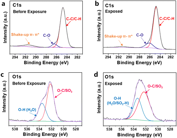
To further understand the mechanism of resist patterning after exposure, the H–SEPS resist films before and after EUV exposure were investigated by X-ray photoelectron spectroscopy (XPS). The high-resolution XPS full-scan survey spectrum of the H–SEPS resist film before and after EUV exposure for 300 s is shown in Fig. S47.† The C1 s spectrum (Fig. 11a) before exposure can be fitted well into three peaks, the binding energies at 284.80, 286.43, and 291.30 eV can be assigned to the bonds of C–C/C–H, C–O, and shake-up π–π* from the polystyrene phenyl ring.40,41 No significant change was observed in the C–O signal after EUV exposure (Fig. 11b), indicating a very small proportion of Ar–OS bond cleavage by EUV irradiation. It is different from the result that cleavage occurs mainly at Ar–OS for the model compound under UV light in solution. This may be due to the different photochemical reaction conditions. The free radical is easy to migrate in solution and form rearrangement compounds, whereas the migration is limited in polymeric resist films. The XPS spectrum of the O1s envelope (Fig. 11c) is fitted by two peaks as O–H and O–C/SO3 at binding energies of 533.55 and 532.17 eV, respectively, which come from the water adsorbed by the film42 and the sulfonate ester group.42,43 After EUV irradiation, the peak of O–H bonding energy shifts from 533.55 to 533.36 eV (Fig. 11d), suggesting the formation of the new SO3–H bond.44 In addition, the bond energies of the SO3 group shifted from 532.17 to 532.31 eV after irradiation, indicating a change in the SO3 group. This result is consistent with the conversion of sulfonate ester to sulfonic acid. The intensity of the SO3 signal decreased, which was attributed to the decomposition of sulfonic acid, and is consistent with observation in situ outgassing analysis.
 |
| | Fig. 11 C1 s core XPS spectra of the H–SEPS resist films (a) before and (b) after EUV exposure for 300 s; XPS of O1 s core spectra of the H–SEPS resist films (c) before and (d) after EUV exposure for 300 s. | |
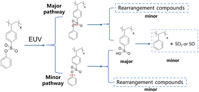
Combining the above experimental results and previous reports,27,34 the exposure mechanism of the H–SEPS resist film was proposed, as shown in Fig. 12. The aryl sulfonate ester groups in the H–SEPS resist film decompose upon EUV exposure, with the cleavage of the ArO–S bond being the major pathway and the Ar–OS bond being the minor pathway. Both pathways produce sulfonic acid and a small amount of rearrangement compounds. A few of the sulfonic acid is further decomposed into gas fragments. These decompositions of aryl sulfonate into polar sulfonic acid groups, along with minor rearrangement, lead to a solubility switch of resist films in the developer after exposure, forming negative-tone patterns. The exposure mechanism of the resist is similar in EBL and EUVL. Previous studies have confirmed that similar chemical reactions occur in resist films upon e-beam and EUV irradiation, both of which generate secondary electrons to induce chemical reactions.45,46
 |
| | Fig. 12 Proposed exposure mechanism of the H–SEPS resist film by EUV irradiation. | |
2.7 Etching resistance of the X–SEPS resists
The etching resistance is an important parameter for the resist to transfer the lithographic pattern to the substrate. To evaluate the etching resistance of the aryl sulfonate ester-modified polymer resists, the H–SEPS and MeO–SEPS resists, which can form high-resolution patterns by EBL, were etched using a dry plasma technique. A pattern of 1.5 × 1.5 μm2 square formed by EBL was etched using an SF6/O2 mixture at −110 °C for 10 s. After etching, the resist residue was removed using a plasma cleaning machine, and the heights of the pattern at each process were characterized by AFM. The 3D AFM images of the H–SEPS resist patterns before and after etching and after resist stripping, together with the cross-sectional morphology and height values, are shown in Fig. 13. The height of the photolithographic pattern before etching was 45 nm. The height after etching was 193 nm. After resist stripping, the height is 166 nm. Therefore, the etching depths of the resist and silicon wafer were 18 and 166 nm, giving the etching rate of the H–SEPS resist film and the silicon wafer 1.8 and 16.6 nm s−1, respectively. The etching selectivity of the H–SEPS resist on the silicon substrate was 9.2:1. The etching resistance of MeO–SEPS resist was measured in the same way, resulting in an etching selectivity of 8.8:1. All the aryl sulfonate ester-modified polymer resists exhibited excellent etching resistance, which is much better than that of the commercial PMMA (950 K) resist (∼6:1)47 and is comparable to the iodonium-functionalized polystyrene resists (9.5:1).38
 |
| | Fig. 13 AFM topography images and sectional profiles of the H–SEPS resist pattern (a) before etching, (b) after etching, and (c) after resist stripping. | |
3 Conclusions
In conclusion, we designed and prepared three kinds of n-CARs based on aryl sulfonate ester-modified polystyrenes (X–SEPS, X = H–, MeO–, and CN–). They exhibit completely different EBL performances. The QCM analysis combined with the bond energy calculation confirms that the influence of the substituent groups on the solubility behavior of the resist films in developers leads to different photolithographic performances. The H–SEPS resist was further optimized to achieve an 18 nm dense L/S pattern and a 10 nm semi-dense L/4S pattern by EBL. Further EUVL performance demonstrates that the H–SEPS resist can form the 22 nm HP patterns. The mechanism study shows that the decomposition of aryl sulfonate to sulfonic acid is the major pathway leading to the solubility switch of the resist film. This study demonstrates that the lithographic performance of n-CARs based on an aryl sulfonate ester-sensitive group can be modulated by changing the substituent. The modifications of substituent groups mainly change the solubility of the resist film rather than the bond energy of the sensitive group, providing useful guidelines for the design and development of n-CARs. A further study of the resist to EUVL for high-resolution patterns is currently underway.
4 Experimental section
4.1 Reagent and synthesis process
The initiator 2,2′-azobis(2-methylpropionitrile) (AIBN) was used after recrystallization with ethanol twice. Other standard reagents were purchased from commercial sources and used as received without further purification. The synthetic procedure of the X–SEPS is shown in Scheme 1. Detailed synthesis steps and characterization data are presented in the ESI.†
4.2 Analytical measurements
5–10 mg of the sample was dissolved in 0.5 mL of deuterated dimethyl sulfoxide (DMSO-d6) or deuterated chloroform (chloroform-d) and analyzed by proton nuclear magnetic resonance (1H NMR) spectrometry on an Ascend 600 M. The mass-to-charge ratio (m/z) and infrared characteristic absorption frequency of the monomers were determined by high-resolution mass spectra (HR-MS) Solarix FTICR mass spectrometers and Fourier transform infrared spectroscopy (FTIR) Excalibur 3100, respectively. The polymer molecular weight (Mw) and polydispersity index (PDI) were tested using gel permeation chromatography (GPC) (Wyatt DAWN Series), with tetrahydrofuran as the mobile phase and a flow rate of 1.0 mL min−1. The thermal decomposition temperature (Td) and glass transition temperature (Tg) of the polymer were measured under a nitrogen atmosphere using an integrated thermal analyzer JCT-1 and a differential scanning calorimeter (DSC) PerkinElmer DSC 4000, respectively, at a temperature rise rate of 10 °C min−1. The resist films were prepared using a coating machine CEE200X and Apogee Bake Plate, and their thickness was measured using a spectroscopic ellipsometer ES01A-DU. The initial exposure of the photoresist film was performed using a 254 nm mercury lamp CEL-LPH120-254. The mask used for the 254 nm exposure was purchased from Beijing China Sciences Shengze Electric Company Limited, with a mask resolution of 1 μm. Electron beam lithography (EBL) was performed using the electron beam exposure system Vistec EBPG 5000 plus ES at a beam current of 100 pA and an acceleration voltage of 100 kV. The extreme ultraviolet (EUV) lithography of the resist film was carried out on a soft X-ray interference lithography beamline (BL08U1B) at the Shanghai Synchrotron Radiation Facility. In situ outgassing analysis was performed using quadrupole mass spectrometry (QMS). The lithographic patterns were captured by a Regulus 8230 scanning electron microscope (SEM) at an accelerated voltage of 1.0 kV. To characterize the surface topography of the resist films, atomic force microscope (AFM) images were captured using the Dimension FastscanBio system in tapping mode. A fully automated dissipative quartz crystal microbalance (QCM) analyzer (QSense Omni) was used to characterize the dissolution behavior of resist films in developers. The etching resistance of the resist films was tested using a plasma etcher, (Sentech/Etchlab 200). The plasma cleaner CPC-F was used to remove the residual resist after etching. X-ray photoemission spectroscopy (XPS), ESCALAB 250Xi, was used for mechanistic investigation.
4.3 Preparation of resists and their films
The polymer was dispersed in PGMEA or PGMEA/cyclohexanone mixture (due to the poor solubility of CN–SEPS in PGMEA, 25 v% cyclohexanone was added to PGMEA for CN–SEPS resist preparation), and a transparent and uniform polymer solution was obtained after stirring for 2 h. The polymer solution was filtered using a 0.22 μm polytetrafluoroethylene filter to give a resist solution with a concentration of 20–50 mg mL−1. The resist solutions were spin-coated directly on two-inch bare silicon wafers at a rotational speed of 2000–5000 revolutions per minute (RPM) to obtain uniform films. After baking for 180 s on a bake plate at 100 °C, the thicknesses of the resist films were measured using a spectroscopic ellipsometer. The thickness of the resist film can be controlled by changing the concentration of the resist solution and the spin coating speed. For example, an H–SEPS resist solution of 23 mg mL−1 provides a resist film with a thickness of 34 nm at a speed of 3500 RPM.
4.4 QCM analysis of the resist films
The resist solution with a concentration of 50 mg mL−1 was spun on the Au substrate of the QCM analyzer at 2000 RPM, and a post-application bake (PAB) at 100 °C for 180 s was applied to the film-coated substrate to remove excess solvent. During the test, the flow rate of the developer was 30 μL min−1, the development time was 5–10 min, and the sampling interval was 0.2 s.
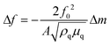
The QCM analyzer is a well-known method for testing the dissolution dynamics of the resist film during the development process.48,49 The QCM can detect extremely small mass changes in the nanogram order from the quartz crystal's resonant frequency during in situ development. The relationship between frequency change Δf and mass change Δm in the QCM test is shown as formula (2):
| |  | (2) |
where
f0 is the resonant frequency,
A is the area of the gold electrode on the quartz substrate,
ρq is the quartz crystal density, and
μq is the shear modulus.
50 The increase in frequency corresponds to the dissolution of the material, whereas the decrease in frequency corresponds to the swelling of the material.
49,51
Data availability
The data supporting this article have been included as part of the ESI.†
Author contributions
R. P. performed the synthesis, experimental measurements, and manuscript drafting. P. L. was involved in the theoretical calculation of bond energy. J. C. proposed the idea, conducted experiments, analyzed data, and performed manuscript drafting and review. T. Y., Y. Z., S. W., X. G., and R. H. were involved in the design of experiments, analytical characterizations, data analysis, and discussions. J. Z. and Y. W. performed the EUV lithographic experiment and participated in discussions. G. Y. helped design the synthetic route, data analysis and discussion, and manuscript review. Y. L. supervised the overall study, characterizations, and manuscript review.
Conflicts of interest
The authors declare no competing financial interests.
Acknowledgements
This work was supported by the National Natural Science Foundation of China (22090012, 22475224). The Chinese Academy of Sciences (CAS) is gratefully acknowledged. We also thank the National Center for Nanoscience and Technology for EBL experiments.
References
- Y. Zhang, H. Yu, L. Wang, X. Wu, J. He, W. Huang, C. Ouyang, D. Chen and B. E. Keshta, Advanced lithography materials: From fundamentals to applications, Adv. Colloid Interface Sci., 2024, 329, 103197–103197 CrossRef CAS PubMed.
- T. Manouras and P. Argitis, High sensitivity resists for EUV lithography: A review of material design strategies and performance results, Nanomaterials, 2020, 10, 1593 CrossRef CAS PubMed.
- S. Hu, J. Chen, T. Yu, Y. Zeng, S. Wang, X. Guo, G. Yang and Y. Li, A novel dual-tone molecular glass resist based on adamantane derivatives for electron beam lithography, J. Mater. Chem. C, 2022, 10, 9858–9866 RSC.
- M. Hassaan, U. Saleem, A. Singh, A. J. Haque and K. Wang, Recent advances in positive photoresists: Mechanisms and fabrication, Materials, 2024, 17, 2552 CrossRef CAS PubMed.
- J. W. Thackeray, Materials challenges for sub-20-nm lithography, J. Micro/Nanolithogr., MEMS, MOEMS, 2011, 10, 033009 CrossRef.
- S. Ghosh, C. P. Pradeep, S. K. Sharma, P. G. Reddy, S. P. Pal and K. E. Gonsalves, Recent advances in non-chemically amplified photoresists for next generation IC technology, RSC Adv., 2016, 6, 74462–74481 RSC.
- L. Li, X. Liu, S. Pal, S. Wang, C. K. Ober and E. P. Giannelis, Extreme ultraviolet resist materials for sub-7 nm patterning, Chem. Soc. Rev., 2017, 46, 4855–4866 RSC.
- M. Yasuda, M. Koyama, K. Imai, M. Shirai, H. Kawata and Y. Hirai, Stochastic simulation of pattern formation for negative-type chemically amplified resists in extreme ultraviolet lithography, J. Photopolym. Sci. Technol., 2020, 33, 53–56 CrossRef CAS.
- S. Hu, J. Chen, T. Yu, Y. Zeng, X. Guo, S. Wang, G. Yang and Y. Li, Photoresists based on bisphenol A derivatives with tert-butyl ester groups for electron beam lithography, J. Photochem. Photobiol., A, 2023, 436, 114351 CrossRef CAS.
- S. Hu, J. Chen, T. Yu, Y. Zeng, G. Yang and Y. Li, Chemically amplified resist based on dendritic molecular glass for electron beam lithography, Chem. Res. Chin. Univ., 2023, 39, 139–143 CrossRef CAS.
- Y. Wang, J. Chen, Y. Zeng, T. Yu, X. Guo, S. Wang, T. Allenet, M. Vockenhuber, Y. Ekinci, J. Zhao, S. Yang, Y. Wu, G. Yang and Y. Li, Molecular glass resists based on tetraphenylsilane derivatives: Effect of protecting ratios on advanced lithography, ACS Omega, 2022, 7, 29266–29273 CrossRef CAS PubMed.
- Y. Wang, J. Yuan, J. Chen, Y. Zeng, T. Yu, X. Guo, S. Wang, G. Yang and Y. Li, A single-component molecular glass resist based on tetraphenylsilane derivatives for electron beam lithography, ACS Omega, 2023, 8, 12173–12182 CrossRef CAS PubMed.
- K. Lawrie, I. Blakey, J. Blinco, R. Gronheid, K. Jack, I. Pollentier, M. J. Leeson, T. R. Younkin and A. K. Whittaker, Extreme ultraviolet (EUV) degradation of poly(olefin sulfone)s: Towards applications as EUV photoresists, Radiat. Phys. Chem., 2011, 80, 236–241 CrossRef CAS.
- P. G. Reddy, S. P. Pal, P. Kumar, C. P. Pradeep, S. Ghosh, S. K. Sharma and K. E. Gonsalves, Polyarylenesulfonium salt as a novel and versatile nonchemically amplified negative tone photoresist for high-resolution extreme ultraviolet lithography applications, ACS Appl. Mater. Interfaces, 2017, 9, 17–21 CrossRef CAS PubMed.
- S. K. Sharma, S. P. Pal, P. G. Reddy, P. Kumar, S. Ghosh and K. E. Gonsalves, Design and development of low activation energy based nonchemically amplified resists (n-CARs) for next generation EUV lithography, Microelectron. Eng., 2016, 164, 115–122 CrossRef CAS.
- A. Rathore, I. Pollentier, H. Singh, R. Fallica, D. De Simone and S. De Gendt, Effect of molecular weight on the EUV-printability of main chain scission type polymers, J. Mater. Chem. C, 2020, 8, 5958–5966 RSC.
- P. G. Reddy, P. Kumar, S. Ghosh, C. P. Pradeep, S. K. Sharma and K. E. Gonsalves, Organic-inorganic hybrid photoresists containing hexafluoroantimonate: Design, synthesis and high resolution EUV lithography studies, Mater. Chem. Front., 2017, 1, 2613–2619 RSC.
- C. A. da Silva Moura, G. K. Belmonte, P. G. Reddy, K. E. Gonslaves and D. E. Weibel, EUV photofragmentation study of hybrid nonchemically amplified resists containing antimony as an absorption enhancer, RSC Adv., 2018, 8, 10930–10938 RSC.
- J. Peter, M. G. Moinuddin, S. Ghosh, S. K. Sharma and K. E. Gonsalves, Organotin in nonchemically amplified polymeric hybrid resist imparts better resolution with sensitivity for next-generation lithography, ACS Appl. Polym. Mater., 2020, 2, 1790–1799 CrossRef CAS.
- M. Yogesh, M. G. Moinuddin, M. Chauhan, S. K. Sharma, S. Ghosh and K. E. Gonsalves, Organoiodine functionality bearing resists for electron-beam and helium ion beam lithography: Complex and sub-16 nm patterning, ACS Appl. Electron. Mater., 2021, 3, 1996–2004 CrossRef CAS.
- H. An, J. Chen, Y. Zeng, T. Yu, S. Wang, X. Guo, R. Hu, P. Tian, M. Vockenhuber, D. Kazazis, Y. Ekinci, G. Yang and Y. Li, Increasing the sensitivity of nonchemically amplified resists by oxime sulfonate-functionalized polystyrene, ACS Appl. Polym. Mater., 2024, 6, 5374–5384 CrossRef CAS.
- H. An, P. Lian, J. Chen, T. Yu, Y. Zeng and Y. Li, Nonchemically-amplified resists based on photosensitive oxime ester functionalized polystyrene, Acta Polym. Sin., 2024, 55, 1313–1324 CAS.
- M. Yoshiwa, H. Kageyama, Y. Shirota, F. Wakaya, K. Gamo and M. Takai, Novel class of low molecular-weight organic resists for nanometer lithography, Appl. Phys. Lett., 1996, 69, 2605–2607 CrossRef.
- N. A. Kuznetsova, G. V. Malkov and B. G. Gribov, Photoacid generators. Application and current state of development, Russ. Chem. Rev., 2020, 89, 173–190 CrossRef CAS.
- T. Shinozuka, M. Shirai and M. Tsunooka, Polymers as sulfonic acid generator on irradiation at 146 nm, Eur. Polym. J., 2001, 37, 1625–1634 CrossRef CAS.
- H. Shiraishi, N. Hayashi, T. Ueno, T. Sakamizu and F. Murai, Novolak resin-based positive electron-beam resist system utilizing acid-sensitive polymeric dissolution inhibitor with solubility reversal reactivity, J. Vac. Sci. Technol., B, 1991, 9, 3343–3347 CrossRef CAS.
- X. Lopez de Pariza, E. Cordero Jara, N. Zivic, F. Ruiperez, T. E. Long and H. Sardon, Novel imino- and aryl-sulfonate based photoacid generators for the cationic ring-opening polymerization of ε-caprolactone, Polym. Chem., 2021, 12, 4035–4042 RSC.
- M. Watanabe, S. Sasaki, S. Yabe and T. Taguchi, Thin resist process having high dry etching resistance in 0.13 μm KrF lithography, Proc. SPIE, 2001, 4345, 580–591 CrossRef CAS.
- G. H. Ho, C.-H. Shao, J.-J. Sung, F.-H. Kang, C.-B. Kao, W.-L. Hung, Y.-L. Chou and Y.-H. Huang, Outgassing and photochemical studies of photosensitive films upon irradiation at 13.5 nm, J. Vac. Sci. Technol., B, 2012, 30, 051602 CrossRef.
- T. Qu, G. Nan, Y. Ouyang, B. Bieketuerxun, X. Yan, Y. Qi and Y. Zhang, Structure-property relationship, glass transition, and crystallization behaviors of conjugated polymers, Polym., 2023, 15, 4268 CAS.
- Z. Wang, J. Chen, T. Yu, Y. Zeng, X. Guo, S. Wang, T. Allenet, M. Vockenhuber, Y. Ekinci, G. Yang and Y. Li, Sulfonium-functionalized polystyrene-based nonchemically amplified resists enabling sub-13 nm nanolithography, ACS Appl. Mater. Interfaces, 2023, 15, 2289–2300 CrossRef CAS PubMed.
- X.-Y. Lu, H. Luo, K. Wang, Y.-Y. Zhang, X.-F. Zhu, D. Li, B. Ma, S. Xiong, P. F. Nealey, Q. Li and G.-P. Wu, CO2-based dual-tone resists for electron beam lithography, Adv. Funct. Mater., 2021, 31, 2007417 CrossRef CAS.
-
M. A. M. H. J. Levinson, F. Cerrina, R. D. Allen, J. G. Skinner, A. R. Neureuther, M. C. Peckerar, F. K. Perkins and M. J. Rooks, Handbook of Microlithography, Micromachining, and Microfabrication, SPIE Press, 1997 Search PubMed.
- E. Torti, G. Della Giustina, S. Protti, D. Merli, G. Brusatin and M. Fagnoni, Aryl tosylates as non-ionic photoacid generators (PAGs): Photochemistry and applications in cationic photopolymerizations, RSC Adv., 2015, 5, 33239–33248 RSC.
- G. H. Bernstein, D. A. Hill and W. P. Liu, New high-contrast developers for poly(methyl methacrylate) resist, J. Appl. Phys., 1992, 71, 4066–4075 CrossRef CAS.
- K. Kasahara, H. Xu, V. Kosma, J. Odent, E. P. Giannelis and C. K. Ober, Nanoparticle photoresist studies for EUV lithography, Proc. SPIE, 2017, 10143, 1014308 CrossRef.
- X. Yuan, J. Chen, T. Yu, Y. Zeng, X. Guo, S. Wang, R. Hu, P. Tian, M. Vockenhuber, D. Kazazis, Y. Ekinci, J. Zhao, Y. Wu, G. Yang and Y. Li, Nonchemically amplified molecular resist based on multi-sulfonium modified triptycene for electron beam and extreme ultraviolet lithography, J. Micro/Nanopatterning, Mater., Metrol., 2024, 23, 034601 CAS.
- X. Yao, P. Lian, J. Chen, Y. Zeng, T. Yu, S. Wang, X. Guo, R. Hu, P. Tian, M. Vockenhuber, D. Kazazis, Y. Ekinci, G. Yang and Y. Li, Iodonium functionalized polystyrene as non-chemically amplified resists for electron beam and extreme ultraviolet lithography, RSC Appl. Polym., 2024, 2, 870–879 RSC.
- G. Lim, K. Lee, C. Koh, T. Nishi and H. J. Yoon, Multinuclear tin-based macrocyclic organometallic resist for EUV photolithography, ACS Mater. Au, 2024, 4, 468–478 CrossRef CAS PubMed.
- V. S. V. Satyanarayana, F. Kessler, V. Singh, F. R. Scheffer, D. E. Weibel, S. Ghosh and K. E. Gonsalves, Radiation-sensitive novel polymeric resist materials: Iterative synthesis and their EUV fragmentation studies, ACS Appl. Mater. Interfaces, 2014, 6, 4223–4232 CrossRef CAS PubMed.
- C. Dezanet, D. Dragoe, P. Marie, N. Harfouche, S. Froissart, A. Fouchet, J. Rouden, J. Lecourt, C. Harnois, P. Thebault, J. Baudoux and B. Lepoittevin, Zirconia surface polymer grafting via dopamine-assisted co-deposition and radical photopolymerization, Prog. Org. Coat., 2022, 173, 107202 CrossRef CAS.
- J. Wolska, K. Stawicka and J. Walkowiak-Kulikowska, Sulfonic-acid-functionalized polymers based on fluorinated methylstyrenes and styrene as promising heterogeneous catalysts for esterification, Mater. Chem. Phys., 2021, 273, 125132 CrossRef CAS.
- G. K. Belmonte, C. A. da Silva Moura, P. G. Reddy, K. E. Gonsalves and D. E. Weibel, EUV photofragmentation and oxidation of a polyarylene - Sulfonium resist: XPS and NEXAFS study, J. Photochem. Photobiol., A, 2018, 364, 373–381 CrossRef CAS.
- Q. Zhang, R. Huang, H. Yao, X. Lu, D. Yan and J. Xin, Removal of Zn2+ from polyethylene terephthalate (PET) glycolytic monomers by sulfonic acid cation exchange resin, J. Environ. Chem. Eng., 2021, 9, 105326 CrossRef CAS.
- Y. Wang, J. Chen, Y. Zeng, T. Yu, S. Wang, X. Guo, R. Hu, P. Tian, M. Vockenhuber, D. Kazazis, Y. Ekinci, Y. Wu, S. Yang, J. Zhao, G. Yang and Y. Li, Nonchemically amplified molecular resists based on sulfonium-functionalized sulfone derivatives for sub-13 nm nanolithography, ACS Appl. Nano Mater., 2023, 6, 18480–18490 CrossRef CAS.
- M. S. M. Saifullah, A. K. Rajak, K. A. Hofhuis, N. Tiwale, Z. Mahfoud, A. Testino, P. Karadan, M. Vockenhuber, D. Kazazis, S. Valiyaveettil and Y. Ekinci, Approaching angstrom-scale resolution in lithography using low-molecular-mass resists (<500 Da), ACS Nano, 2024, 18, 24076–24094 CrossRef CAS PubMed.
- X. Cong, S. Zhang, J. Gao, X. Cui, Y. Wu, X. Guo, R. Hu, S. Wang, J. Chen, Y. Li and G. Yang, Novel etch-resistant molecular glass photoresist based on pyrene derivatives for electron beam lithography, ACS Omega, 2024, 9, 37585–37595 CrossRef CAS PubMed.
- M. Toriumi, Theoretical analysis of development behavior of resist measured by QCM, Proc. SPIE, 2009, 7273, 72732Y CrossRef.
- M. Harumoto, J. J. Santillan, T. Itani and T. Kozawa, Dependence of photoresist dissolution dynamics in alkaline developers on alkyl chain length of tetraalkylammonium hydroxide, Jpn. J. Appl. Phys., 2022, 61, 056506 CrossRef CAS.
- G. Sauerbrey, Verwendung von Schwingquarzen zur Wägung dünner Schichten und zur Mikrowägung, Z. Phys., 1959, 155, 206–222 CrossRef CAS.
- N. Maeda, A. Konda, K. Okamoto, T. Kozawa and T. Tamura, Resist thickness dependence of line width roughness of chemically amplified resists used for electron beam lithography, Jpn. J. Appl. Phys., 2020, 59, 086501 CrossRef CAS.
Footnote |
| † Electronic supplementary information (ESI) available: Synthesis procedure and characterization; physical properties of aryl sulfonate ester polymers X–SEPS; 254 nm photolithography; bond energy computation; LER measurement of high-resolution SEM images; mechanism study of the X–SEPS resist. See DOI: https://doi.org/10.1039/d5im00046g |
|
| This journal is © Institute of Process Engineering of CAS 2025 |
Click here to see how this site uses Cookies. View our privacy policy here. 
 Open Access Article
 This Open Access Article is licensed under a Creative Commons Attribution-Non Commercial 3.0 Unported Licence
 *a,
Tianjun
Yu
*a,
Tianjun
Yu