DOI:
10.1039/D5EL00034C
(Paper)
EES Sol., 2025,
1, 356-365
A hydrophobic organic spacer cation for improving moisture resistance and efficiency in mixed-dimensional perovskite solar cells†
Received
13th March 2025
, Accepted 19th April 2025
First published on 24th April 2025
Abstract
Mixed-dimensional perovskite structures containing two-dimensional (2D) bulky organic cations offer enhanced stability but suffer from lower efficiency compared to their three-dimensional (3D) counterparts. To overcome the stability limitations while maintaining high efficiency, we introduce a hydrophobic sulfoxonium cation for mixed-dimensional perovskite solar cells (MxD-PSCs). Herein, we employ a novel triple organic cation comprising methylammonium iodide (MAI), formamidinium iodide (FAI), and trimethylsulfoxonium chloride (TMSCl) to formulate MAFA(TMS)xPbI3−xClx perovskites. The incorporation of TMSCl enhances moisture resistance due to its superior hydrophobicity, while also improving charge transfer and reducing non-radiative recombination as confirmed by optical, morphological, and electrical characterizations. The optimized MxD-PSCs achieve a remarkable power conversion efficiency (PCE) of 21.43%, VOC of 1.10 V, and JSC of 24.82 mA cm−2, with FF being enhanced to 78.5% under one-sun illumination (AM 1.5G). Moreover, optimized MxD-PSCs also perform exceptionally with a PCE of 34.18% under indoor lighting (1000 lux). Furthermore, the devices exhibit outstanding stability, retaining 85% of their initial efficiency after 90 days in an inert environment and 84% after 1000 hours under ambient conditions. These findings highlight the potential of the TMSCl cation for enhancing both the stability and PCE of MxD-PSCs, offering a promising pathway for the development of long-lasting and high-performance PSCs.
Broader context
Perovskite solar cells (PSCs) offer high efficiency but face stability issues, especially under moisture exposure. Mixed-dimensional perovskites combine 2D and 3D structures to enhance stability, though efficiency can be compromised. Introducing hydrophobic spacer cations, like trimethylsulfoxonium chloride, can improve both moisture resistance and performance. This research highlights a promising approach for developing durable and efficient PSCs.
|
Introduction
Hybrid metal halide perovskites represent the most promising next-generation photovoltaic (PV) materials, exhibiting exceptional optoelectronic characteristics, including a high photon absorption coefficient, extensive charge-carrier diffusion length, high charge-carrier mobility, and effective photo-generated exciton dissociation with low fabrication cost.1–5 The power conversion efficiency (PCE) of perovskite solar cells (PSCs) has significantly risen from 3.8% to more than 26% under one-sun illumination, matching that of crystalline silicon (c-Si) and other inorganic thin-film PVs.6 Various groupings of A, B, and X categories provide distinct types of perovskite materials for PSC applications, each exhibiting a unique crystal structure and optoelectronic capabilities. Specifically, methylammonium lead iodide (MAPbI3) is extensively utilized as an effective perovskite material in PSCs.7 However, this kind of perovskite is not stable and deteriorates when subjected to heat, oxygen, moisture, and light.8 Conversely, formamidinium lead iodide (FAPbI3) serves as a viable alternative to MAPbI3 for enhancing the stability of PSCs. This perovskite demonstrates an enhanced performance with an absorption onset at the near-infrared (NIR) region at approximately 840 nm, approaching the Shockley–Queisser limit. It also exhibits superior thermal stability, reduced volatility of FA+ relative to MA+, and more robust hydrogen bonding between FA+ and PbI6 compared to MA+ and PbI6.9,10 But, the application of FAPbI3 in PSCs is hampered by the superficial phase transitions of α-FAPbI3 to δ-FAPbI3 at room temperature (RT).11 Hence, numerous strategies have been explored for the commercial implementation of PSCs, with sequential deposition methods and compositional engineering for developing mixed-cation perovskites by different research groups. Grätzel et al. initially introduced the idea of mixed perovskites by integrating FA+ and MA+ at the A site to formulate (MA)x(FA)1−xPbI3 perovskite.12 The results indicated that δ-phase FAPbI3 can be entirely eliminated in (MA)x(FA)1−xPbI3 perovskite, with the resulting PSCs attaining a PCE of 14.9% by the sequential deposition approach with better stability. Furthermore, Saliba et al. reported FA+, MA+, and Cs+ MxD perovskites that effectively stabilize α-FAPbI3.13 This facilitates more reproducible PSC performances, achieving a steady power output of 21.1% and maintaining 18% after 250 h under operative conditions. Still, the triple mixed perovskite layers minimally impede defects between the grains and fail to ensure prolonged stability. Similarly, various research groups have investigated large organic ammonium cations such as guanidinium (GA+), phenethylammonium (PEA+), benzyl ammonium (BA+), etc. in MxD-PSCs, which demonstrated enhanced stability relative to pure MAPbI3 and FAPbI3-based PSCs.14–16 However, the long-term stability of these larger organic ammonium cation mixed hybrid PSCs has not been comprehensively effective, as amines are prone to react in the presence of moisture through hydrogen bonding.17 In recent years, sulfur-based cations are garnering increasing interest compared to organic ammonium cations for the development of moisture-stable PSCs, specifically 2-thiophene-methylamine (TMA+), 2-thiopheneethylamine (TEA+), butyldimethylsulfonium (BDMS+), trimethylsulfoxonium (TMS+) etc.18,19 The stability mostly arises from the absence of hydrogen bonding between the sulfur-based cations and H2O molecules, along with the robust electrostatic interactions between these cations and the PbI6. Amongst these, it has been shown that the novel sulfur-based TMS+ cation may interact with metal halides to create stable perovskites. Kaltzoglou et al. synthesized trimethylsulfonium iodide and examined its structural and optoelectronic characteristics, demonstrating remarkable stability under humid air conditions and at temperatures up to 200 °C for the first time.20 Furthermore, Parashar et al. demonstrated the integration of TMS+ cations into MAPbI3, resulting in the formation of mixed-dimensional perovskites (TMSPbI3)x(MAPbI3)100−x, which exhibit improved moisture resistance and a power conversion efficiency equivalent to pristine MAPbI3.21 Recent studies have explored the incorporation of several iodine-based organic cations and chloride-based cations, such as MACl and FACl, to improve the stability and performance of PSCs. Chloride-based cations provide several advantages over iodine-based organic cations, including the suppression of ion migration, enhancement of film crystallinity, defect passivation, long electron/hole diffusion length, carrier lifetime, strain alleviation, acceleration of low-dimensional stable phase formation, and are also advantageous for indoor light conditions with facile bandgap tuning.22–25 However, organic cations containing sulfur and chlorine have not been explored much due to several factors such as solubility, boiling point, and larger size; also it is quite challenging to replace Cl− with I− in perovskites.26
In this work, we have reported a novel organic triple-cation MxD-PSC that consists of MA+, FA+, and TMS+, forming a stable MAFA(TMS)xPbI3−xClx perovskite. The optimized incorporation of TMSCl stabilized the perovskite phase, enhanced crystallinity, and facilitated the formation of a defect-free and compact morphology compared to the pristine perovskite (PVK). Subsequently, the optimized MAFA(TMS)xPbI3−xClx-based MxD-PSCs showed a PCE of 21.43% compared to 17.82% for the reference device under AM 1.5G (1 sun) conditions. Moreover, MxD-PSCs also demonstrated a promising performance with a PCE of 34.18% under indoor light conditions (1000 lux). The unencapsulated MxD-PSC also showed enhanced stability, retaining 85% of its initial performance after 90 days in an inert atmosphere and 84% after 1000 hours under ambient conditions.
Results and discussion
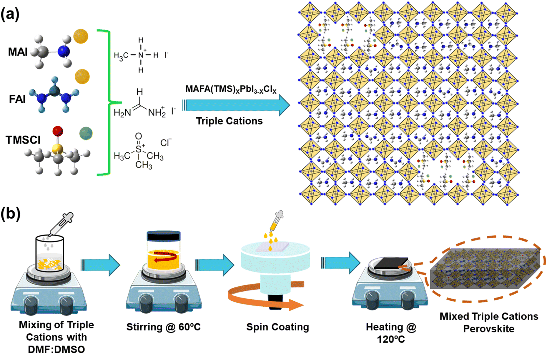
To elucidate the influence of the TMSCl salt, MxD perovskite was made both with and without the addition of this salt. Fig. 1a illustrates the development of an organic triple cation perovskite, defined by the formula MAFA(TMS)xPbI3−xClx for stable MxD-PSCs. The SnO2 layer was deposited on the ITO glass substrate with a spin coater, and then an MxD-perovskite layer was deposited on the top of the ITO/SnO2 by a one-step solution processing method using antisolvent engineering methodology inside an N2-filled glovebox as shown in Fig. 1b.
 |
| | Fig. 1 (a) Schematic representation of the MxD perovskite structure incorporating triple organic cations, depicting the arrangement of cations within the perovskite lattice. (b) Illustration of the fabrication process of MxD perovskite films, showing the sequential steps involved in film deposition, including precursor preparation, spin coating, annealing, and crystallization to achieve high-quality perovskite films. | |
The influence of TMSCl addition on the optical characteristics of MxD perovskite films was investigated using a UV-vis absorption spectrum, as seen in Fig. 2a. The perovskite film doping with 1 mg TMSCl displays an inclusive enhancement in absorbance compared to that of the doping with 0.5 mg TMSCl and pristine perovskite (PVK) film. The enhanced absorption property of 1 mg doped film is attributed to homogeneous crystal formation and superior perovskite film quality, while perovskite films with increased TMSCl concentrations (2 mg, 4 mg and 8 mg) exhibit reduced absorbance due to inadequate film covering and many voids (Fig. S1†).
 |
| | Fig. 2 Schematic of (a) the UV-vis absorption spectrum, (b) steady state PL spectra, (c) TRPL graphs of perovskites with or without TMSCl doping, (d) XRD graph, (e) enlargement of XRD graphs at lower angles, and (f) raman spectrum of the perovskite layer and doping with different concentrations of TMSCl. | |
Steady-state PL has been employed to examine the charge dynamics in PVK and doping with varying amounts of TMSCl additive in PVK as presented in Fig. 2b. The intensities of the PL peaks significantly increased with TMSCl doping from 0.5 mg to 1 mg, accompanied by a slight blue shift in the emission peak that followed the incorporation of TMSCl with the perovskite lattice. The enhanced PL intensities indicate a high crystal quality and improved charge transfer within the active layer.27,28 In contrast, perovskite films with increased TMSCl concentrations (2 mg, 4 mg, and 8 mg) exhibit low intensities with red shift due to a decrease in the quality of films (Fig. S2†). Additionally, the time resolved PL (TRPL) analysis shows that the photogenerated carriers have longer lifetime (5.58 ns) in case of the 1 mg TMSCl doped film which is notably greater than that of the PVK film (1.46 ns) as shown in Fig. 2c. The carrier lifetime study for varying TMSCl doping amounts in PVK was further investigated (Fig. S3†). It appears that the 1 mg TMSCl doped film is appropriate for reducing defects and promotes improved perovskite crystallization and development because a further increase in the TMSCl concentration (2, 4, and 8 mg) did not prolong the carrier decay time. The TRPL data has been fitted with the biexponential decay function (the fitting results have been summarized in Table S1†).29 The longer carrier lifetime indicates low nonradiative recombination as a result of reduced trap states in the perovskite layer and facilitated charge transport and these TRPL findings correlate with the steady state PL as well.30,31 The crystal structures of pristine and TMSCl doped perovskite films were examined using X-ray diffraction (XRD), with the resultant XRD patterns illustrated in Fig. 2d. The XRD patterns indicate that the 1 mg doped TMSCl film has a high intensity at 14.58°, representing perovskite films, compared to the 0.5 mg (14.52°) and pristine (14.52°) samples. Moreover, the associated PbI2 peaks at 13.14° progressively diminish subsequent doping with the TMSCl. As shown in Fig. 2e, under the conditions of 0.5 mg and 1 mg doping amounts of TMSCl, new diffraction peaks from 6° to 12° are observed in XRD patterns that might be related to the formation of a typical low dimensional perovskite via integration of TMSCl within the perovskite lattice.32,33 The XRD results demonstrate that an appropriate amount (1 mg) of TMSCl doping improves the crystallinity and film quality of the pristine perovskite film, corroborating the absorption and PL data. Opportunely, we discovered that the MxD-perovskite, when subjected to higher concentration doping, displays distinctive diffraction peaks at low angles (11.28° & 9.28°) with greater intensities compared to the peak at 14.86°, indicating the formation of a unique MxD-perovskite, MAFA(TMS)xPbI3−xClx (Fig. S4†). It is noted that when concentration increases, the associated peak of the perovskite shifts to higher values, namely 1 mg (14.58°) and 8 mg (14.86°). Moreover, the absorption spectra and the XRD graph of (TMS)xPbI2−xClx are illustrated in Fig. S5.† This finding confirmed that the interaction of TMSCl cations with PVK is responsible for the peaks at low angles. The vibrational modes of the perovskite films doped with different concentrations of the TMSCl cation were analysed using Raman spectroscopy with 532 nm laser excitation. To achieve adequate roughness for perovskite crystal growth, perovskite films were fabricated on ITO/SnO2 substrates rather than glass, leading to reduced spectral intensity owing to the quenching effect of the SnO2 layer.34 The raman peak of the pristine film appears at ∼95.23 cm−1 and the peaks of films doped with 0.5 mg and 1 mg TMSCl are slightly shifted to lower wave numbers at ∼91.58 cm−1 and ∼88.58 cm−1, respectively. A transition to lower wavenumbers indicates a reduction in bond stiffness, likely due to the elongation of the Pb–I bond by Cl substitution.35 This change may signify the emergence of more stable or extended phases with modified halide compositions.36 The interactions of the TMSCl doped in PVK (0.5, 1, 2, 4 and 8 mg) and (TMS)xPbI2−xClx were examined using Fourier transform infrared spectroscopy (FTIR), depicted in Fig. S6.† For the TMSCl doped perovskite, we found that N–H stretching peaks arise between 3000 and 3300 cm−1 and at 3402 cm−1 while there is no N–H peak for (TMS)xPbI2−xClx.37 Consequently, S![[double bond, length as m-dash]](https://www.rsc.org/images/entities/char_e001.gif) O stretching peaks occur at 1027 cm−1 and 1235 cm−1 for doped TMSCl films.38,39 These peaks evenly reduce from (TMS)xPbI2−xClx to 0.5 mg for the TMSCl doped film and disappear in pure PVK. These alterations are attributed to the robust interaction between TMSCl cations in PVK.
O stretching peaks occur at 1027 cm−1 and 1235 cm−1 for doped TMSCl films.38,39 These peaks evenly reduce from (TMS)xPbI2−xClx to 0.5 mg for the TMSCl doped film and disappear in pure PVK. These alterations are attributed to the robust interaction between TMSCl cations in PVK.
Top-view scanning electron microscopy (SEM) images were recorded to examine the influence of the TMSCl addition on perovskite film crystallization and grain size. Fig. 3a–c display the SEM images and respective grain distribution graphs of PVK and with 0.5 mg and 1 mg of TMSCl as an additive. It can be observed that the grain size of PVK is relatively smaller with an average grain size of 450 nm having a large number of grain boundaries with various cracks. In addition, the 0.5 mg and 1 mg TMSCl-doped PVK films exhibit grain sizes of 500 nm and 600 nm, respectively, which are larger than that of the PVK film. Nevertheless, defects/pinholes existed in the 0.5 mg TMSCl doped PVK film which were substantially removed after the doping amount of TMSCl was increased to 1 mg in PVK. The morphology of the optimized 1 mg doped film was also improved, showing a grain size as large as 1 μm and demonstrating stick type grains. Further overdosing of TMSCl (2, 4, and 8 mg) resulted in disrupted perovskite grain growth with disadvantageous formation of grains having more pinholes and a texture-like non-uniform surface as shown in Fig. S7.† The excessive use of additives in perovskite precursors influences the nucleation kinetics, hence altering the grain size and development.40 Moreover, a high concentration of the additive may influence the solubility of particular intermediates in the homogeneous solution, potentially leading to the precipitation of perovskite crystals and variations in grain sizes.41 Another potential cause may be the alteration in surface energy due to the excessive treatment with TMSCl, which affected the texture of the resultant film. The variations in surface energy may alter the interaction between the perovskite layer and substrate, resulting in distinct roughness or morphologies.42 These results demonstrate that the optimal amount of TMSCl in PVK not only regulates crystallization and grain formation but also aids in reducing Pb, which limits charge generation and extraction abilities in MxD-PSCs.43 Furthermore, detection of chlorine incorporation in PVK has been demonstrated by energy dispersive X-ray spectroscopy (EDS). It helps in ascertaining if chlorine has been effectively incorporated into the crystal lattice or is only present on the surface or grain boundaries. This indicates that chlorine is evenly distributed and concentrated at grain boundaries as the doping amount of TMSCl in PVK increases (Fig. S8†). Additionally, the surface morphology and potential of perovskites were examined before and after TMSCl doping using atomic force microscopy (AFM) and kelvin probe force microscopy (KPFM) as shown in Fig. 3d–g. Doping with 1 mg TMSCl in PVK directed to a reduction in the root-mean-square surface roughness from 72 nm in the PVK film to 61.4 nm. The reducing surface roughness signifies that the doping with TMSCl effectively passivates the defects at the grain boundary and inside the grains.39 Additionally, KPFM was used to analyse the potential of perovskite films and their surface work function in order to demonstrate the surface trap state. Here, contact potential difference (CPD) and surface work function can be derived from 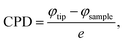 where φtip and φsample are the work function of the tip and perovskite films, and e is elementary charge.44 As per KPFM, the average CPD of PVK and doping with 1 mg TMSCl in PVK films are −144 ± 5 mV and 28 ± 5 mV, respectively. Also, surface work functions of PVK and 1 mg TMSCl doped PVK are calculated to be 4.844 eV and 4.672 eV for PVK, respectively. It can be observed that the TMSCl doped film has a lower work function, indicating a low density of electron trap states. This can inhibit the recombination of free holes and trapped electrons.45 Furthermore, the line profile graphs of PVK and TMSCl doped films signify that the film surface of doped PVK has a lower CPD change and a superior film quality as shown in Fig. 3h. To evaluate the variation in surface potential, KPFM line profiles were extracted across multiple grains and grain boundaries for both pristine and TMSCl-doped perovskite films. In the pristine perovskite, pronounced CPD dips were observed at the grain boundaries, indicating significant band bending due to charged defect states. This suggests the presence of strong local electric fields, which could act as non-radiative recombination centers. In contrast, the TMSCl-doped film exhibited a much flatter CPD profile, with minimal potential variation across grain boundaries. This flattening of potential reveals reduced trap densities and improved electronic uniformity, confirming the effectiveness of TMSCl in mitigating bulk defect states.46,47
 |
| | Fig. 3 (a)–(c) Top-view SEM pictures of PVK and with different amounts of TMSCl cation and alongside statistical distribution of the grain sizes for corresponding SEM images, AFM and KPFM images of (d) and (e) PVK film, (f) and (g) 1 mg TMSCl doping in PVK, and (h) line profile graph of KPFM (for interpretation of the references to colour in this figure legend, the reader is referred to the web version of this article). | |
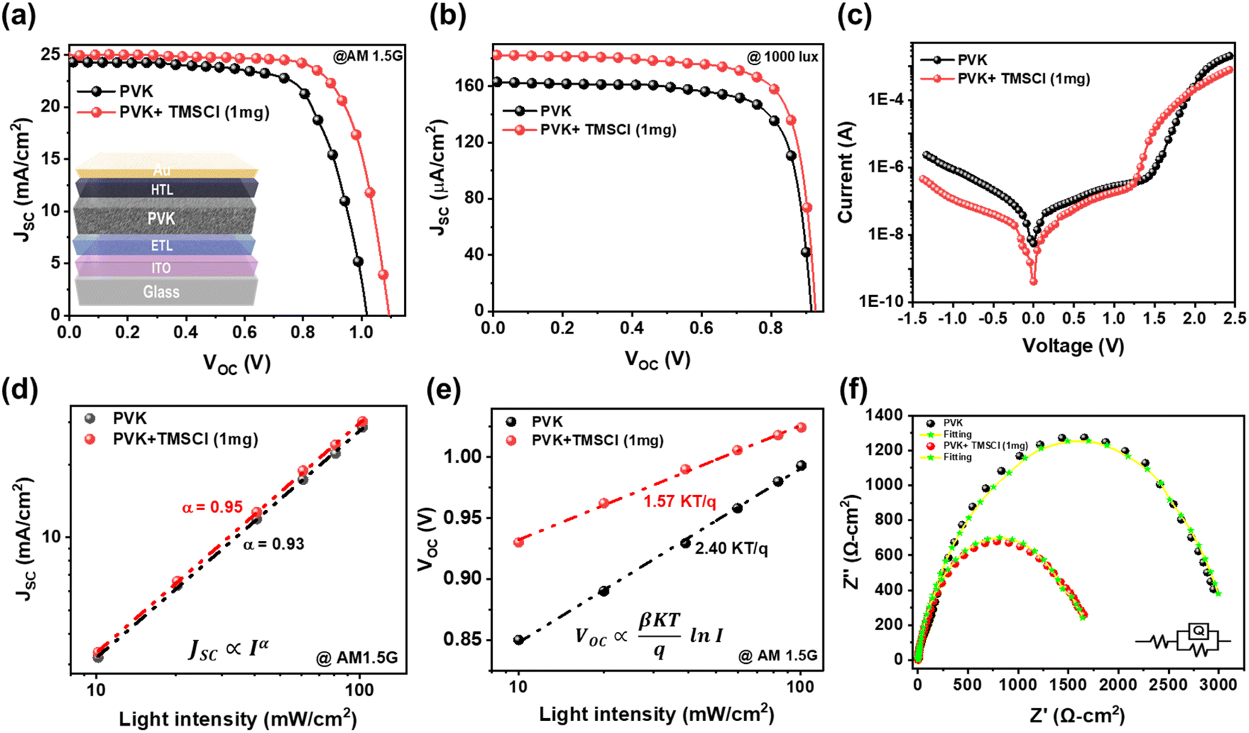
The fabrication methodology of our MxD-PSCs is broadly discussed in the experimental section of the ESI.† We have fabricated n-i-p based ITO/SnO2/PVK/spiro-OMeTAD/Au structured devices with doping of various amounts (0.5 mg, 1 mg, 2 mg, 4 mg and 8 mg) of TMSCl. Fig. 4a showed the optimized J–V curves with or without TMSCl additive doping, the PVK exhibited a PCE of 17.82% with a VOC of 1.02 V, a JSC of 24.46 mA cm−2, and a fill factor (FF) of 71.60%. For the 1 mg TMSCl doped device, the champion PCE increased to 21.43% with a VOC of 1.10 V, JSC of 24.82 mA cm−2, and enhanced FF of 78.5%, where a remarkable improvement in FF was observed under one sun conditions. However, doping with TMSCl also displayed remarkable performance under indoor light conditions compared to PVK as shown in Fig. 4b. The PVK device showed a PCE of 29.85% with a JSC of 162.98 μA cm−2, a VOC of 0.916 V, and FF of 74.20%; the 1 mg TMSCl doped device exhibited a PCE of 34.18%, a JSC of 182.15 μA cm−2, a VOC of 0.927 V, and 75.1% FF under 1000 lux LED illumination. Additionally, we have performed the J–V measurements with different doping amounts of TMSCl in PVK under both indoor and outdoor conditions (Fig. S9, S10, Tables S2 and S3†). It is observed that excessive doping of TMSCl cations disrupts the overall performance of the device which results in adverse effects.48Fig. 4c displays the dark I–V curves of devices, and the dark current after 1 mg TMSCl doping is one order of magnitude lower than that of the PVK device. Dark current is associated with charge recombination and the lower dark current shows suppressed charge recombination by TMSCl doping.49 Furthermore, to comprehend the charge carrier recombination mechanism in PVK and with 1 mg doping in PVK, the dependency of the JSC with light intensity (JSC ∝ Iα) was considered under light intensity ranging from 10 to 100 mW cm−2. JSCversus light intensity displays a linear relationship in dual-log scale, as shown in Fig. 4d. The fitted α values of PVK (0.93) and with 1 mg TMSCl doping (0.95) indicate low bimolecular recombination in the TMSCl doping assisted device, that can be attributed to the high-quality films with lower grain boundary defects.50,51 The semi-log plot of VOC as a function of light intensity for both the PSCs and the slopes results from the lines linearly fitted to the values as shown in Fig. 4e. The PVK demonstrates an effective dependency of VOC on the light intensity, with a slope of 2.40 KT/q, where K is Boltzmann constant, q is elementary charge, and T is absolute temperature. The device doped with 1 mg TMSCl displays a lower slope value of 1.90 KT/q, representing reduced trap-assisted Shockley–Read–Hall recombination, that is attributed to the improved crystallinity of the film with decreased trap defect sites as well as hindered ion migration due to the integration of TMSCl cations.37 Similarly, PVK with 1 mg doped TMSCl shows lower bimolecular and Shockley–Read–Hall recombination under indoor light intensities ranging from 250 to 1500 lux as shown in Fig. S11.† The electrical parameters, including J–V characteristics and intensity dependency analysis of devices, are summarized in Table 1. We quantitatively determined the respective resistances and recombinational phenomenon of devices with different TMSCl doping amounts using electrochemical impedance spectroscopy (EIS) in order to confirm the enhanced PV performance through the charge transfer process under a dark environment and short circuit conditions. The Nyquist plots of the device without and with 1 mg TMSCl doping and the curves are fitted by the equivalent circuit as shown in Fig. 4f. The PVK shows a series resistance (RSe) of 2.24 Ω cm2, a charge transfer resistance (Rct) of 3144 Ω cm2, and the device with 1 mg TMSCl shows RSe and Rct of 1.91 Ω cm2 and 1625 Ω cm2, respectively. The reduced Rct indicates that TMSCl doping effectively suppresses charge recombination in the device. The corresponding device parameters with variation of TMSCl doping are summarized in Fig. S12 and Table S4.† It has been observed that the high amount of TMSCl cation led to recombination which limited the charge transport process, subsequently increasing the Rct.52
 |
| | Fig. 4 The current density–voltage (J–V) curves for PVK and TMSCl doped PVK under (a) one sun conditions (the inset figure shows the fabricated n-i-p PSC structure, ETL – SnO2 and HTL – spiro-OMeTAD), (b) indoor lighting conditions, and (c) dark conditions. (d) Short circuit current density (JSC) versus light intensity plot under one sun conditions, (e) open-circuit voltage (VOC) versus light intensity plot under one sun conditions, and (f) the EIS spectra with an equivalent circuit diagram for PVK and 1 mg doped PVK devices. | |
Table 1 PV parameters of the PVK and 1 mg doping of TMSCl in PVK for outdoor and indoor environments
| Light source |
Device |
V
OC (V) |
J
SC (mA cm−2 μA−1 cm−2) |
FF (%) |
PCE (%) |
α
|
β
|
|
α and β are related to bimolecular recombination & trap-assisted recombination as discussed in the text.
|
| Outdoor (AM1.5G) |
PVK |
1.02 |
24.46 |
71.26 |
17.82 |
0.93 |
2.40 |
| PVK + TMSCl (1 mg) |
1.10 |
24.82 |
78.50 |
21.43 |
0.95 |
1.57 |
| Indoor (1000 lux) |
PVK |
0.91 |
162.98 |
73.90 |
29.85 |
0.78 |
1.91 |
| PVK + TMSCl (1 mg) |
0.93 |
182.15 |
75.10 |
34.18 |
0.80 |
1.52 |
We studied the long-term stability of the unencapsulated PSCs under the inert and ambient conditions (RH 50% ± 7%) as shown in Fig. 5a and b. It was found that PVK with TMSCl doping unveils significantly improved stability compared to the PVK device. The aforementioned investigations provide support for these results, which demonstrate that TMSCl-doped PVK is usually more stable than pristine PVK due to several kinds of physicochemical interactions that enhance its structural, chemical, and environmental resilience. Furthermore, as the hydrophobic nature of the perovskite plays a significant role in their moisture stability, the water dampening performance of different perovskite films was examined in Fig. 5c. The 1 mg TMSCl cation incorporated PVK film displays a contact angle of 85°, which is larger than that of the PVK film (73°), demonstrating that the doped PVK is more hydrophobic. Fig. 5d depicts the contact angles of the water drop on PVK and doped PVK films with different loading times. When the water loading time increased to 60 s, the doped PVK film still maintained a high contact angle of 58°, which is higher than that of the PVK film (45°) (Fig. S13†). Furthermore, we tested the hydrophobicity of MAFA, TMSCl, and (TMS)xPbI2−xClx films on the ITO/SnO2 substrate as shown in Fig. S14 and S15.† We observed that the TMSCl (51°) is more hydrophobic than MAFA (18°). Interestingly, (TMS)xPbI2−xClx displayed super hydrophobicity with a contact angle of 95.5°. The results suggest that the PVK with TMSCl doping could be more efficient in protecting the perovskite film from moisture and improving the stability. The percentage drop in PCE (inert and ambient conditions) and contact angle (0 to 5 s) is illustrated in Table 2. Additionally, we performed contact angle measurements at different doping amounts of TMSCl (0.5, 2, 4, and 8 mg) in PVK (Fig. S16†).
 |
| | Fig. 5 Stability analysis for unencapsulated PVK and TMSCl-doped devices (a) under inert conditions (devices were kept in a desiccator after each measurement), (b) under ambient conditions (RH 50% ± 7%), (c) schematic images of contact angles of a water droplet on PVK and 1 mg doped TMSCl films, and (d) contact angle vs. time graph of PVK and 1 mg TMSCl doped PVK films. | |
Table 2 Summary of device stability and time-dependent contact angle measurements for various deposited films
| Device |
Drop in PCE (Δη%) |
| Inert conditions for 90 days |
Ambient conditions for 1000 h |
| PVK |
46.2 |
39.1 |
| PVK + TMSCl (1 mg) |
13.5 |
12.9 |
| Various deposited films |
Change in contact angle after 5 seconds (Δθ%) |
| ITO/SnO2/MAFA |
50 |
| ITO/SnO2/TMSCl |
11.8 |
| ITO/SnO2/PVK |
17.8 |
| ITO/SnO2/PVK + TMSCl (1 mg) |
2.4 |
| ITO/SnO2/(TMS)xPbI2−xClX |
3.6 |
In this work, we investigated how mixing the TMSCl in PVK improves the optical, structural, chemical, and electrical properties in devices with the variation of doping amount. It has been observed that after doping of TMSCl, the Cl atoms distributed more at grain boundaries rather than inside grains as depicted in Fig. 6a. This indicates that Cl atoms at grain boundaries mitigate defects, enhance crystallinity, and stabilize the lattice, which collectively reduce recombination, improve charge transport, and increase the operational stability of PSCs.53,54 To further verify this hypothesis, we performed EDS point mapping of PVK films with different concentrations of TMSCl cations and we found that the weight percentage of Cl atoms is more at the grain boundary region as compared to inside grains (Fig. S17†). Upon increasing the amount of TMSCl from 0.5 mg to 8 mg, the Cl weight percentage varied as depicted in Fig. 6b. At the highest amount of TMSCl doping, the Cl atoms are distributed uniformly at grain boundaries and throughout grains, in contrast to the optimum doping amount. Fig. 6c illustrates the generalized depiction of TMSCl doping in PVK, confirming experimentally that an increased number of Cl atoms assists in passivating the grain boundaries in PVK films.
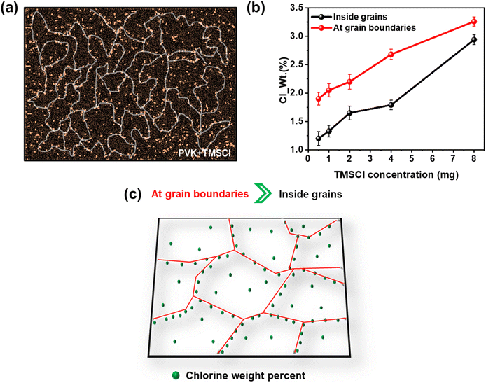 |
| | Fig. 6 (a) EDS image of TMSCl doped PVK with chlorine (Cl) weight percentage at grain boundaries, (b) graph of chlorine weight percent with the variation of TMSCl doping amount, and (c) schematic of (Cl) distribution within the PVK film morphology after TMSCl doping. | |
Conclusions
In summary, we investigated the role of TMSCl in the morphology and optoelectronics properties of a novel triple cation MxD-PSC. We find that the optimized doping amount of TMSCl in PVK leads to the formation of perovskite films with larger grains, high quality of films with high optoelectronic characteristics, and better stability than the PVK device. Furthermore, MxD-PSCs demonstrated a PCE of 21.43%, under AM 1.5G and also performed exceptionally under indoor conditions (1000 lux) with a PCE of 34.18%. The MxD-PSCs also displayed enhanced stability, maintaining 85% of the initial value after 90 days (inert conditions) and 84% of the initial values after 1000 hours under an ambient environment (RH 50% ± 7%). The TMSCl assisted PVK device unveiled excellent hydrophobicity by displaying extraordinary moisture resistance without any kind of encapsulation. Our investigations indicate that the use of TMSCl doping in PVK precursors provides favorable results for the advancement of highly efficient and durable PSCs, facilitating the commercialization of this technology.
Data availability
The data that support the findings of this study are available in the ESI.†
Conflicts of interest
The authors declare there is no conflict of interest.
Acknowledgements
R. S. wishes to thank the Science and Engineering Research Board (SERB), New Delhi, India for the Core Research Grant, (grant no. CRG/2022/003088) SERB project and Indian Institute of Technology Mandi for providing the experimental facilities at the Advanced Material Research Centre (AMRC) and Centre for Design & Fabrication of Electronic Devices (C4DFED).
References
- N. J. Jeon,
et al., A fluorene-terminated hole-transporting material for highly efficient and stable perovskite solar cells, Nat. Energy, 2018, 3(8), 682–689 CrossRef CAS.
- W. Nie,
et al., High-efficiency solution-processed perovskite solar cells with millimeter-scale grains, Science, 2015, 347(6221), 522–525 CrossRef CAS PubMed.
- G. Xing,
et al., Low-temperature solution-processed wavelength-tunable perovskites for lasing, Nat. Mater., 2014, 13(5), 476–480 CrossRef CAS.
- P. Kumar,
et al., Research progress and challenges in extending the infra-red absorption of perovskite tandem solar cells, Nano Energy, 2023, 109175 Search PubMed.
- S. D. Stranks,
et al., Electron-hole diffusion lengths exceeding 1 micrometer in an organometal trihalide perovskite absorber, Science, 2013, 342(6156), 341–344 CrossRef CAS.
-
C. Castañeda, et al., Machine learning algorithms for predicting electrical performance of perovskite solar cells, in 2024 IEEE Technology and Engineering Management Society (TEMSCON LATAM), IEEE, 2024 Search PubMed.
- N. J. Jeon,
et al., Compositional engineering of perovskite materials for high-performance solar cells, Nature, 2015, 517(7535), 476–480 CrossRef CAS PubMed.
- B. Conings,
et al., Intrinsic thermal instability of methylammonium lead trihalide perovskite, Adv. Energy Mater., 2015, 5(15), 1500477 CrossRef.
- Y. Liu,
et al., Stabilization of highly efficient and stable phase-pure FAPbI3 perovskite solar cells by molecularly tailored 2D-overlayers, Angew. Chem., Int. Ed., 2020, 59(36), 15688–15694 CrossRef CAS PubMed.
- J. Jeong,
et al., Pseudo-halide anion engineering for α-FAPbI3 perovskite solar cells, Nature, 2021, 592(7854), 381–385 CrossRef CAS PubMed.
- M. Lyu,
et al., Effect of additives AX (A= FA, MA, Cs, Rb, NH4, X= Cl, Br, I) in FAPbI3 on photovoltaic parameters of perovskite solar cells, Sol. RRL, 2020, 4(10), 2000331 CrossRef CAS.
- N. Pellet,
et al., Mixed-organic-cation perovskite photovoltaics for enhanced solar-light harvesting, Angew. Chem., Int. Ed., 2014, 53(12), 3151–3157 CrossRef CAS PubMed.
- M. Saliba,
et al., Cesium-containing triple cation perovskite solar cells: improved stability, reproducibility and high efficiency, Energy & Environ. Sci., 2016, 9(6), 1989–1997 RSC.
- W. Zhang,
et al., Guanidinium induced phase separated perovskite layer for efficient and highly stable solar cells, J. Mater. Chem. A, 2019, 7(16), 9486–9496 RSC.
- R. Hu,
et al., Enhanced stability of α-phase FAPbI 3 perovskite solar cells by insertion of 2D (PEA) 2 PbI 4 nanosheets, J. Mater. Chem. A, 2020, 8(16), 8058–8064 RSC.
- A. Q. Alanazi,
et al., Benzylammonium-mediated formamidinium lead iodide perovskite phase stabilization for photovoltaics, Adv. Funct. Mater., 2021, 31(30), 2101163 CrossRef CAS.
- J. Y. Ye,
et al., Enhancing charge transport of 2D perovskite passivation agent for wide-bandgap perovskite solar cells beyond 21%, Solar RRL, 2020, 4(6), 2000082 CrossRef CAS.
- C. Ge,
et al., Mixed dimensional perovskites heterostructure for highly efficient and stable perovskite solar cells, Sol. RRL, 2022, 6(4), 2100879 CrossRef CAS.
- M. Kundar,
et al., Stable perovskite solar cells based on direct surface passivation employing 2D perovskites, Sol. RRL, 2023, 7(23), 2300572 CrossRef CAS.
- A. Kaltzoglou,
et al., Trimethylsulfonium lead triiodide: an air-stable hybrid halide perovskite, Inorg. Chem., 2017, 56(11), 6302–6309 CrossRef CAS.
- M. Parashar,
et al., Formation of 1-D/3-D fused perovskite for efficient and moisture stable solar cells, ACS Appl. Energy Mater., 2021, 4(3), 2751–2760 CrossRef CAS.
- X. Liu,
et al., Advances in chloride additives for high-efficiency perovskite solar cells: multiple points of view, Chem. Commun., 2023, 59(90), 13394–13405 RSC.
- C. Zuo,
et al., An 80.11% FF record achieved for perovskite solar cells by using the NH4 Cl additive, Nanoscale, 2014, 6(17), 9935–9938 RSC.
- A. H. Howlader,
et al., Progress and challenges of chloride–iodide perovskite solar cells: a critical review, Nanomanufacturing, 2023, 3(2), 177–216 CrossRef.
- J. Kim,
et al.
, Chlorine incorporation in perovskite solar cells for indoor light applications, Cell Rep. Phys. Sci., 2020, 1(12), 100273 CrossRef CAS.
- L. Yang,
et al., Recent progress and challenges of organometal halide perovskite solar cells, Rep. Prog. Phys., 2016, 79(2), 026501 CrossRef PubMed.
- C. Luo,
et al., Engineering the buried interface in perovskite solar cells via lattice-matched electron transport layer, Nat. Photonics, 2023, 17(10), 856–864 CrossRef CAS.
- Y. Wu,
et al., Stable perovskite solar cells with 25.17% efficiency enabled by improving crystallization and passivating defects synergistically, Energy Environ. Sci., 2022, 15(11), 4700–4709 RSC.
- X. Zheng,
et al., Dual functions of crystallization control and defect passivation enabled by sulfonic zwitterions for stable and efficient perovskite solar cells, Adv. Mater., 2018, 30(52), 1803428 CrossRef.
- G. Kim,
et al., Impact of strain relaxation on performance of α-formamidinium lead iodide perovskite solar cells, Science, 2020, 370(6512), 108–112 CrossRef CAS PubMed.
- J.-W. Lee,
et al., Solid-phase hetero epitaxial growth of α-phase formamidinium perovskite, Nat. Commun., 2020, 11(1), 5514 CrossRef CAS.
- P. Chen,
et al., In situ growth of 2D perovskite capping layer for stable and efficient perovskite solar cells, Adv. Funct. Mater., 2018, 28(17), 1706923 CrossRef.
- H. Wang,
et al., Phenyltrimethylammonium chloride additive for highly efficient and stable FAPbI3 perovskite solar cells, Nano Energy, 2024, 123, 109423 CrossRef CAS.
- P. Pansa-Ngat,
et al., Mechanical and electrical comparative studies of widely utilized solar perovskite thin films via scanning probe microscopy, ACS Appl. Energy Mater., 2024, 7(8), 3234–3244 CrossRef CAS.
- R. G. Niemann,
et al., Halogen effects on ordering and bonding of CH3NH3+ in CH3NH3PbX3 (X = Cl, Br, I) hybrid perovskites: a vibrational spectroscopic study, J. Phys. Chem. C, 2016, 120(5), 2509–2519 CrossRef CAS.
- S. Ghosh,
et al., Raman spectroscopy of formamidinium-based lead mixed-halide perovskite bulk crystals, ChemPhysChem, 2023, 24(21), e202300303 CrossRef CAS PubMed.
- T. Zhou,
et al., Highly efficient and stable solar cells based on crystalline oriented 2D/3D hybrid perovskite, Adv. Mater., 2019, 31(32), 1901242 CrossRef PubMed.
- C. Deng,
et al., Modulating residual lead iodide via functionalized buried interface for efficient and stable perovskite solar cells, ACS Energy Lett., 2022, 8(1), 666–676 CrossRef.
- C. Deng,
et al.
, Solvation-driven grain boundary passivation improving the performance of perovskite solar cells, Adv. Energy Mater., 2024, 14(10), 2303387 CrossRef CAS.
- J. Zhao,
et al., Exploring the film growth in perovskite solar cells, J. Mater. Chem. A, 2021, 9(10), 6029–6049 RSC.
- J. Jiao,
et al., Solvent engineering for the formation of high-quality perovskite films: a review, Results Eng., 2023, 18, 101158 CrossRef CAS.
- M. Azam,
et al., Additive engineering enabled non-radiative defect passivation with improved moisture-resistance in efficient and stable perovskite solar cells, Chem. Eng. J., 2024, 483, 149424 CrossRef CAS.
- M. Azam,
et al., Realization of moisture-resistive perovskite films for highly efficient solar cells using molecule incorporation, ACS Appl. Mater. Interfaces, 2020, 12(35), 39063–39073 CrossRef CAS.
- S. Yu,
et al., Hydrazinium cation mixed FAPbI3-based perovskite with 1D/3D hybrid dimension structure for efficient and stable solar cells, Chem. Eng. J., 2021, 403, 125724 CrossRef CAS.
- Z. Kang,
et al., Kelvin probe force microscopy for perovskite solar cells, Sci. China Mater., 2019, 62(6), 776–789 CrossRef CAS.
- C. Lu,
et al., Carrier transfer behaviors at perovskite/contact layer heterojunctions in perovskite solar cells, Adv. Mater. Interfaces, 2019, 6(2), 1801253 CrossRef.
- E. M. Lanzoni,
et al., The impact of Kelvin probe force microscopy operation modes and environment on grain boundary band bending in perovskite and Cu (In, Ga) Se2 solar cells, Nano Energy, 2021, 88, 106270 CrossRef CAS.
- J.-W. Lee,
et al., Rethinking the A cation in halide perovskites, Science, 2022, 375(6583), eabj1186 CrossRef CAS PubMed.
- P. Kumar,
et al., A comprehensive review on dark current in perovskite photodetectors: origin, drawbacks, and reducing strategies, Sens. Actuators, A, 2024, 115076 CrossRef CAS.
- V. Mihailetchi, J. Wildeman and P. W. Blom, Space-charge limited photocurrent, Phys. Rev. Lett., 2005, 94(12), 126602 CrossRef CAS PubMed.
- D. Bi,
et al., Effect of different hole transport materials on recombination in CH3NH3PbI3 perovskite-sensitized mesoscopic solar cells, J. Phys. Chem. Lett., 2013, 4(9), 1532–1536 CrossRef CAS.
- M. Azam,
et al., Organic chloride salt
interfacial modified crystallization for efficient antimony selenosulfide solar cells, ACS Appl. Mater. Interfaces, 2022, 14(3), 4276–4284 CrossRef CAS.
- Q. Chen,
et al., The optoelectronic role of chlorine in CH3NH3PbI3 (Cl)-based perovskite solar cells, Nat. Commu., 2015, 6(1), 7269 CrossRef CAS.
- Y. Wang,
et al., Chlorine passivation of grain boundary suppresses electron–hole recombination in CSPbBr3 perovskite by nonadiabatic molecular dynamics simulation, ACS Appl. Energy Mater., 2019, 2(5), 3419–3426 CrossRef CAS.
|
| This journal is © The Royal Society of Chemistry 2025 |
Click here to see how this site uses Cookies. View our privacy policy here. 
 Open Access Article
 This Open Access Article is licensed under a Creative Commons Attribution-Non Commercial 3.0 Unported Licence
 *ab
*ab

 where φtip and φsample are the work function of the tip and perovskite films, and e is elementary charge.44 As per KPFM, the average CPD of PVK and doping with 1 mg TMSCl in PVK films are −144 ± 5 mV and 28 ± 5 mV, respectively. Also, surface work functions of PVK and 1 mg TMSCl doped PVK are calculated to be 4.844 eV and 4.672 eV for PVK, respectively. It can be observed that the TMSCl doped film has a lower work function, indicating a low density of electron trap states. This can inhibit the recombination of free holes and trapped electrons.45 Furthermore, the line profile graphs of PVK and TMSCl doped films signify that the film surface of doped PVK has a lower CPD change and a superior film quality as shown in Fig. 3h. To evaluate the variation in surface potential, KPFM line profiles were extracted across multiple grains and grain boundaries for both pristine and TMSCl-doped perovskite films. In the pristine perovskite, pronounced CPD dips were observed at the grain boundaries, indicating significant band bending due to charged defect states. This suggests the presence of strong local electric fields, which could act as non-radiative recombination centers. In contrast, the TMSCl-doped film exhibited a much flatter CPD profile, with minimal potential variation across grain boundaries. This flattening of potential reveals reduced trap densities and improved electronic uniformity, confirming the effectiveness of TMSCl in mitigating bulk defect states.46,47