
 Open Access Article
 This Open Access Article is licensed under a
 Creative Commons Attribution 3.0 Unported Licence
Mitigating the amorphization of perovskite layers by using atomic layer deposition of alumina†
Mayank
Kedia
 ab,
Chittaranjan
Das
*ab,
Malgorzata
Kot‡
c,
Yenal
Yalcinkaya
d,
Weiwei
Zuo
b,
Kenedy
Tabah Tanko
e,
Peter
Matvija
f,
Mikel
Ezquer
g,
Iñaki
Cornago
g,
Wolfram
Hempel
h,
Florian
Kauffmann
i,
Paul
Plate
j,
Monica
Lira-Cantu
e,
Stefan A.L.
Weber
ad and
Michael
Saliba
*ab
ab,
Chittaranjan
Das
*ab,
Malgorzata
Kot‡
c,
Yenal
Yalcinkaya
d,
Weiwei
Zuo
b,
Kenedy
Tabah Tanko
e,
Peter
Matvija
f,
Mikel
Ezquer
g,
Iñaki
Cornago
g,
Wolfram
Hempel
h,
Florian
Kauffmann
i,
Paul
Plate
j,
Monica
Lira-Cantu
e,
Stefan A.L.
Weber
ad and
Michael
Saliba
*ab
aInstitute for Photovoltaics (ipv), Research Center SCoPE, and Integrated Quantum Science and Technology Center (IQST), University of Stuttgart, Pfaffenwaldring 47, 70569 Stuttgart, Germany. E-mail: chittaranjan.das@ipv.uni-stuttgart.de; michael.saliba@ipv.uni-stuttgart.de
bHelmholtz Young Investigator Group, IMD-3 Photovoltaik, Forschungszentrum Jülich, 52425 Jülich, Germany
cChair of Applied Physics and Semiconductor Spectroscopy, Brandenburg University of Technology Cottbus-Senftenberg, Konrad-Zuse-Straße 1, 03046 Cottbus, Germany
dMax Planck Institute for Polymer Research, Ackermannweg 10, 55128 Mainz, Germany
eCatalan Institute of Nanoscience and Nanotechnology (ICN2), CSIC and The Barcelona Institute of Science and Technology, Autonomous University of Barcelona, 08193 Bellaterra, Spain
fCharles University, Faculty of Mathematics and Physics, Department of Surface and Plasma Science, V Holešovičkách 2, Prague, Czech Republic
gNational Renewable Energy Centre of Spain (CENER), Ciudad de la Innovación 7, 31621, Sarriguren, Spain
hZentrum für Sonnenenergie und Wasserstoff Forschung Baden-Württemberg (ZSW), 70563 Stuttgart, Germany
iSRF Advanced Materials Innovation and Characterization (AMICA), University of Stuttgart, 70569 Stuttgart, Germany
jSENTECH Instruments GmbH, Schwarzschildstraße 2, 12489 Berlin, Germany
First published on 12th March 2025
Abstract
Atomic layer deposition of aluminum oxide (ALD-Al2O3) layers has recently been studied for stabilizing perovskite solar cells (PSCs) against environmental stressors, such as humidity and oxygen. In addition, the ALD-Al2O3 layer acts as a protective barrier, mitigating pernicious halide ion migration from the perovskite towards the hole transport interface. However, its effectiveness in preventing the infiltration of ions and additives from the hole-transport layer into perovskites remains insufficiently understood. Herein, we demonstrate the deposition of a compact ultrathin (∼0.75 nm) ALD-Al2O3 layer that conformally coats the morphology of a triple-cation perovskite layer. This promotes an effective contact of the hole transporter layer on top of the perovskite, thereby improving the charge carrier collection between these two layers. Upon systematically investigating the layer-by-layer structure of the PSC, we discovered that ALD-Al2O3 also acts as a diffusion barrier for the degraded species from the adjacent transport layer into the perovskite. In addition to these protective considerations, ALD-Al2O3 impedes the transition of crystalline perovskites to an undesired amorphous phase. Consequently, the dual functionality (i.e., enhanced contact and diffusion barrier) of the ALD-Al2O3 protection enhanced the device performance from 19.1% to 20.5%, while retaining 98% of its initial performance compared to <10% for pristine devices after 1500 h of outdoor testing under ambient conditions. Finally, this study deepens our understanding of the mechanism of ALD-Al2O3 as a two-way diffusion barrier, highlighting the multifaceted role of buffer layers in interfacial engineering for the long-term stability of PSCs.
Broader contextDespite achieving high efficiencies, perovskite solar cells struggle with long-term stability, e.g. due to halide migration under illumination and moisture. We reveal that the degradation of the hole-transport layer (HTL) and related degradation by-products into the perovskite leads to its transformation from a crystalline phase to an undesirable amorphous phase. To address this issue, we deposited alumina on the perovskite surface as a compact and conformal interfacial layer using atomic layer deposition. We demonstrate that this protective layer acts as a dual-purpose diffusion barrier. It effectively blocks the ingress of degraded by-products into the perovskite and the egress of halide ions from the perovskite to the HTL, resulting in enhanced stability under operating conditions. This highlights the importance of understanding layer-by-layer degradation under operating conditions to fully elucidate the mechanisms of complete cell degradation. Such insights are crucial for advancing the understanding, development and commercialization of perovskites. |
Introduction
Organic–inorganic halide perovskite solar cells (PSCs) have emerged as a promising thin-film photovoltaic technology, with a current record power conversion efficiency (PCE) of >26%.1,2 However, their long-term stability under the operating conditions hinders commercialization.3,4 The interfaces in a multilayer stack act as a source of defects, leading to intrinsic instabilities.5–7 Various chemical and mechanical passivation techniques, including organic salts, polymers, and laser polishing, effectively mitigate these defects and increase device performance and stability.8–12 However, solvent-based post-treatment processes lack uniform coverage on a larger scale, potentially impacting long-term stability.13–15To overcome these challenges, atomic layer deposition (ALD) has been employed as a strategy for depositing compact thin metal oxides (sub-10 nm) as protective layers, particularly in microelectronics and photovoltaic industries.16–18 In the case of perovskites, several studies have reported the successful application of ALD of alumina (Al2O3) on perovskites at higher temperatures (>100 °C).19–22 This process involves depositing ALD-Al2O3 directly onto perovskites, such as methylammonium lead iodide (MAPbI3), resulting in an improved PCE of ∼18% with improved stability, maintaining 60% of its initial performance after 60 days in an ambient atmosphere with a relative humidity (R.H.) of 40–70%.23 Moreover, Kot et al. utilized room-temperature ALD (RT-ALD) deposition on MAPbI3 to avoid the effect of thermal stress on the perovskite and showed an increase in device performance and stability with an ALD-Al2O3 overlayer on top of the perovskite film over time.24,25
Such notable improvements in device stability are often attributed to the suppression of halide ion migration from MAPbI3 perovskites towards the hole-transport layer (HTL) or the ingress of H2O molecules into perovskites through the ALD-Al2O3 layer.26–28 However, these studies with ALD-Al2O3 passivation focus on “half-cell configurations” of inherently unstable perovskites, leaving the effect of the subsequently deposited charge-transport layer underexplored.19,26,29 Interestingly, the use of additives in spiro-OMeTAD in record-efficiency cells may result in undesirable products that percolate into the perovskite absorber, accelerating degradation and photoinstability.2,30–32 Thus, the protective layer stabilizes against the environment as well as against the adjacent layers.33,34
Despite these promising examples, there is limited evidence in literature on the conformal coverage of (<2 nm) ALD layers. In this study, using conductive atomic force microscopy (c-AFM), we demonstrated the uniform coverage of a ∼0.75 nm thin ALD-Al2O3 layer on top of a standard triple-cation perovskite, including its facets. This homogeneous coverage resulted in a PCE of 20.5% (from 19.1%) without modifying the bulk.35,36 The devices were subjected to shelf-aging (<10% R.H.) for 180 days, followed by 1000 min of maximum power point tracking (MPPT) under ambient conditions (>60% R.H.) to evaluate the shelf and operational stability. The unencapsulated devices with the ∼0.75 nm ALD layer retained 75% of the initial PCE, whereas the control devices retained only 10% of the initial PCE. Furthermore, when conducting outdoor stability tests under ISOS-O-2 protocol for 1500 h, the ALD-protected device maintained >98% of its initial efficiency compared to <10% for the control devices. We also systematically investigated the role of ALD-Al2O3 in enhancing the intrinsic stability of perovskite, with and without the spiro-OMeTAD overlayer. We observed that the ALD-Al2O3 layer improved the contact of the spiro-OMeTAD layer with the perovskite layer, thus mitigating shunting pathways. This compact barrier layer also inhibited the diffusion of byproducts from spiro-OMeTAD degradation under operating conditions into the perovskite. Thus, our study highlights the bifunctional nature of the interfacial diffusion barrier, both as a protection against penetration by extrinsic stressors and in preventing intrinsic outgassing from the active layer.
Results and discussion
Al2O3 barrier layers of various thicknesses were deposited by precisely controlling the number of ALD cycles deposited on a triple-cation (using Cs, MA and formamidinium (FA)) perovskite composition at room temperature. More details on fabrication and characterization can be found in the Experimental Section. The ALD-Al2O3 during deposition was monitored using in situ spectroscopic ellipsometry (SE), as shown in Fig. 1a. After the first few cycles (denoted as “I” for the “initial” ALD growth process), the thickness starts to increase linearly resulting in a “steady” growth regime (II). | ||
| Fig. 1 (a) Variation in stack thickness (ITO/Perovskite/ALD-Al2O3) with the number of ALD cycles measured by in situ spectroscopic ellipsometry. Top-left inset: Device stack. Bottom-right inset: magnified view of the first 30 cycles with two growth modes: initial (I) and steady growth (II). (b) Cross-sectional transmission electron microscopy (TEM) image of a ∼5 nm ALD-coated perovskite on a polished silicon substrate. A 200 nm layer of Pt was deposited to prevent damage to the ALD layer during focused ion beam milling. Insets show selected area diffraction patterns of Al2O3 (amorphous) and perovskite (crystalline). (c) 3D conductive atomic force microscopy (c-AFM) images of the uncoated and ALD-0.75nm films with the current contrast overlaid on the topological images collected over the same area, revealing the microstructure-specific response in the dark at 400 mV. The scale was the same for the uncoated and ALD-0.75nm films and fixed from 16 pA to 18 pA. (d) Current comparison of the perovskite film surface extracted from c-AFM image before and after ∼0.75 nm of ALD-Al2O3. | ||
In the inset of Fig. 1a, a sudden increase in the thickness is observed after the first ALD cycle, as TMA and H2O react to form alumina on top of the perovskite. However, with subsequent ALD cycles, the growth follows a meandering behavior, as the growth is assumed to be island-based because of the presence of various adsorption sites on the perovskite surface or steric hindrance.37 This can be described as the “initial regime” (I) until the perovskite layer is fully covered by the ALD process. From Fig. 1a, it can be assumed that after 10–14 cycles, the linear growth of alumina starts on the perovskite with a conformal thickness of <1 nm. We note that have also obtained a thickness of ∼35.24 nm after 600 ALD cycles on a clean silicon wafer to obtain a growth cycle of 0.057 nm per cycle, see Fig. S1 (ESI†). Thus, in this study, we have assigned a thickness of ∼0.75 nm for the ALD-Al2O3 thin film after 14 ALD cycles at room temperature.
To ensure the deposited ALD layer's conformity and quality, we first investigated a ∼5 nm thick alumina layer on top of the perovskite. In Fig. 1b, we show transmission electron microscopy (TEM) images of the cross-section showing a homogeneous coating of alumina on top of the perovskite surface via ALD, without any discernible discontinuities, even on a larger scale. Furthermore, selected area electron diffraction (SAD) data were collected in these two distinct regions: perovskite and ALD-Al2O3, as shown in Fig. 1b. The SAD pattern from the perovskite region showed randomly overlapping rings with bright spots, indicating the presence of a polycrystalline material. The diffraction patterns from the ALD-Al2O3 spot show a ring pattern that is more diffused and continuous, confirming the presence of an amorphous phase, which is consistent with previous reports.38,39 For ALD film crystallization, typically, a post-annealing treatment using significantly higher temperatures (>200 °C) is required.40 We posit that amorphous Al2O3 can also act as a passivation layer, as previously reported in literature.41,42 Fig. S2 and S3 (ESI†) show the individual elemental mapping and energy-dispersive X-ray (EDX) spectra displaying the uniform distribution of ALD-Al2O3 on the top of perovskite.
Further, we also performed reflection electron energy loss spectroscopy (REELS) to determine the bandgap (Eg) of the ultrathin ALD-2nm film on perovskite. The spectrum of the amorphous ALD-Al2O3 shows a shoulder at 0.71 eV and a broad loss feature at the onset of 3.27 eV in Fig. S4 (ESI†). This value is in close agreement with the previously reported value of ultrathin amorphous alumina (3.2 eV).43 Additionally, unlike stoichiometric and well-ordered crystalline alumina, our measurement also shows the distribution of tail states in the “forbidden” energy gap (shaded in orange). We associate the absence of sharp edges at the onset with the sub-bandgap electronic defects induced by site disorder and ideal vacancies owing to the amorphous and non-stoichiometric ratio of the ALD-Al2O3 layer.
While the coverage of a “thick” ∼5 nm layer benefits stability, it exacerbates the charge extraction.25,44 Therefore, the alumina layer needs to be sufficiently thick to uniformly cover the surface and, at the same time, sufficiently thin to have as low a series resistance as possible. To this end, we deposited ∼0.75 nm (referred to as “ALD-0.75nm”) and ∼2 nm (ALD-2nm) alumina on bare perovskite to ensure maximum perovskite coverage. In Fig. 1c, we map and correlate the local resistive dark current along with the topographic features of the underlying perovskite using conductive atomic force microscopy (c-AFM). Large variations in the current profile of the pristine (referred to as “uncoated”) perovskite film can be observed with the perovskite facets owing to the different orientations of the polycrystalline thin films.45 The ALD-0.75nm has weakened the conductivity of the perovskite film and only some grain tips (from roughness) were not covered. In Fig. 1d, we observed that ALD-0.75nm reduces the total average current by ∼0.20 pA, and the conductivity spread has been minimized, highlighting a uniform coverage of the ALD layer on the perovskite surface. For ALD-2nm, the perovskite was completely covered, including the facets and tips, as shown in Fig. S5 (ESI†). The individual topography maps, along with the current values, are shown in Fig. S6–S8 (ESI†). Additionally, masking the current value has provided us a coverage area of 87.46% after ∼0.75 nm of ALD coverage and 98.03% after 2 nm of ALD coverage. These c-AFM results confirm that an ultrathin ALD layer covers most of the perovskite facets, including the grain boundaries, as also suggested by our in situ spectroscopic ellipsometry results in Fig. 1a. Such a large-area surface coverage uniformity of an ultrathin interfacial layer is noteworthy as conventional solvent-based organic passivation layers tend to accumulate in the dips of the perovskite and passivate only the grain boundaries, as shown by Martins et al.46 However, full coverage by ALD-2nm comes at the cost of a significant loss in the transfer of photogenerated current, as shown in Fig. S19 (ESI†). Thus, in the following sections, we focus on ALD-0.75nm.
Next, the role as barriers of these uniform ALD-0.75nm layers on perovskite were studied in the “half-cell” configuration (without overlying HTL). Fig. 2a shows the top-view scanning electron microscopy (SEM) images of the as-prepared (“Fresh”) uncoated and ALD-0.75nm coated perovskites. The surface morphology of the ALD-0.75nm perovskite was comparable to that of the uncoated perovskite, indicating that the perovskite remained undamaged by the room-temperature ALD process. This contrasts with the reports for MAPbI3 and MAyFA(1−y)Pb(IBr)3, where a porous degradation pattern of >40 nm was observed.26,27 In Fig. 2b, we note that both the ALD-0.75nm and uncoated films started to degrade and developed pinholes under exposure to 1 sun illumination for 1000 min in an atmosphere of >50% R.H. (“Aged”). The damage to the uncoated perovskite was much more severe throughout the surface, including the grain boundaries and also within the grains (highlighted with red circles). We posit that this is because of the possible escape of volatile organic gases from residual solvents or perovskite decomposition upon light and moisture degradation, as previously reported.47–49 For ALD-0.75nm, fewer pinholes were observed within the grains, indicating that the protective alumina barrier reduced the ingress of O2 and H2O.50 Upon light degradation, the absorbance in Fig. 2c also decreased for both the uncoated and ALD-0.75nm perovskites, showing that direct light exposure in ambient conditions accelerates decomposition, as confirmed by the SEM images. Interestingly, in the inset of Fig. 2c, the uncoated film did not show any clear absorption onset around its band gap, whereas the ALD-0.75nm maintains a much sharper absorption onset, indicating that the perovskite retained its original absorber quality.
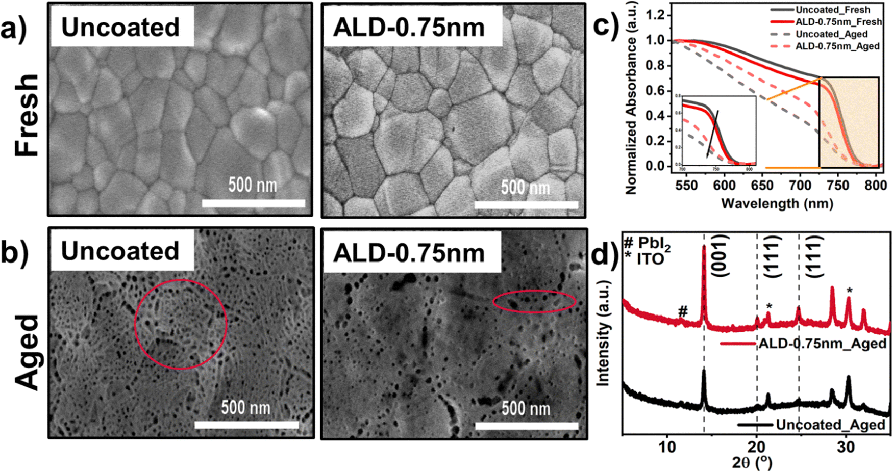 | ||
| Fig. 2 (a) and (b): Top-view of scanning electron microscopy (SEM) images. (c) Normalized absorbance (Inset: The enlarged region around the absorption onset) of the uncoated and ALD-0.75nm films before (Fresh) and after a light soaking test for 1000 min in the ambient atmosphere of >50% R.H. (Aged). (d) X-ray diffraction (XRD) pattern of the uncoated and ALD-0.75nm coated perovskite films after aging. | ||
The X-ray diffraction (XRD) measurements for the fresh ALD-0.75nm and uncoated perovskite were similar (see Fig. S9, ESI†). Fig. 2d shows the XRD reflections at 14.3° for the uncoated and ALD-0.75nm perovskites after light aging. The (001) reflection of the ALD-coated perovskite was almost twice that of the uncoated samples under constant light illumination in an ambient atmosphere (Fig. S10, ESI†). We also note that the PbI2 peak at 12.7° is not as pronounced upon light degradation, even for the uncoated triple-cation perovskite, as it was observed for the MAPbI3 and MAyFA(1−y)Pb(IBr)3 solar cells.26,51 Such observations underline the importance of the perovskite composition and its reactivity towards similar interfacial treatments, producing contrasting results. Based on these experiments, in Fig. S11 (ESI†), we also provide a possible growth mechanism of ALD-Al2O3 on top of FA-dominated perovskite using X-ray photoelectron spectroscopy (XPS). Thus, together with the morphology, crystallinity, and optical properties, it was shown that the ALD-protected perovskite film exhibited a slower intrinsic degradation as atmospheric gases were blocked, e.g., O2 and H2O (even in the presence of light).
In addition, to study the role of alumina as a barrier layer in a back electrode-free device, the spiro-OMeTAD as an HTL was deposited on the uncoated and ALD-0.75nm perovskite films, as shown in Fig. 3a. We performed the aging experiments as mentioned above, i.e., under light and ambient atmospheric conditions (>50% R.H.) for 1000 min. In Fig. 3b, the uncoated film with spiro-OMeTAD turned towards a white, milky color rather than the expected yellow color of the PbI2 phase, which is the commonly reported degradation product of perovskite.52 On the other hand, the ALD-0.75nm sample showed no visible signs of aging. This observation underscores that the role of the ALD-0.75nm barrier depends on the overlying layer. Moreover, this observation also underlines the degradative role of hygroscopic dopants, such as Li-TFSI salt in spiro-OMeTAD.30
 | ||
| Fig. 3 (a) Schematic of the ALD-0.75nm perovskite with a spiro-OMeTAD layer under aging conditions. (b) Optical images. (c) X-ray photoelectron spectra of carbon 1s (C1s) and fluorine 1s (F1s) core levels. (d) X-ray diffraction patterns. (e) Normalized time-of-flight secondary ion mass spectrometry depth profile of individual ions representing spiro-OMeTAD (OMe), CsMAFA perovskite (Pb, MA, FA, I), ITO (Sn), and Al2O3 (Al) layers of the uncoated and ALD-0.75nm films along with the spiro-OMeTAD layer fresh and after light aging under ambient conditions (>50% R.H.). | ||
To understand the chemical changes in spiro-OMeTAD in a full device during long-term operation, we performed in-operando near-ambient pressure X-ray photoelectron spectroscopy (NAP-XPS) measurements on the perovskite/(ALD-Al2O3)/spiro-OMeTAD stack. The C1s and F1s spectra have shifted to higher binding energy (B.E.) by ∼0.3 and ∼0.5 eV upon light illumination in the uncoated and ALD-0.75nm stack, as shown in Fig. 3c. The higher shift in the B.E. is consistent with the higher photovoltages in the ALD-0.75nm perovskite.53,54 The spectra of all the other elements are shown in Fig. S12 (ESI†). Further, to observe the chemical changes on the spiro-OMeTAD surface, we applied accelerated aging conditions, i.e., illumination at 80 °C, 1 mbar H2O and O2 atmosphere. The C1s and F1s spectra shift back to their respective dark peaks (indicated by the smaller arrows in Fig. 3c) for the ALD-0.75nm films, even under illumination. This confirms the loss in surface photovoltage due to chemical changes in the spiro-OMeTAD under light and moisture, independent of the buried interface.55,56 Interestingly, the C1s and F1s spectra in the uncoated sample moved to an even lower binding energy (shown by the larger arrow to the right in Fig. 3c, which might have been caused by the chemical reduction of spiro-OMeTAD owing to a damaged interface in the unencapsulated sample.57 Additionally, the I3d5/2 peak for both the uncoated and ALD-0.75nm is substantially low (compared to fresh samples) on the spiro-OMeTAD surface, even upon aging under light and moisture (see Fig. S13, ESI†).
XRD measurements were performed on the above-mentioned fresh and aged films to reveal the changes in the perovskite/(ALD-0.75nm)/spiro-OMeTAD bulk structural properties. The XRD measurement of the uncoated sample in the presence of spiro-OMeTAD showed a PbI2 peak before light aging, unlike the ALD-0.75nm samples, as shown in Fig. S14 (ESI†). This could indicate that the degradation mechanism of perovskite is different in the “half-cell” configuration as compared to that in the presence of spiro-OMeTAD film under aging conditions. Upon light and moisture aging, the perovskite peaks started disappearing in the uncoated sample. Additionally, an increase in the amorphous background is displayed in Fig. 3d. This 100% reduction in the scattering intensity of the uncoated sample indicates the absence of long-range order in the perovskite structure, pointing towards amorphization, as reported by Abate et al.58,59 A small peak was observed at 11.6°, while no PbI2 and perovskite peaks were observed in the uncoated sample. This indicates the possible transition of the perovskite to the FAPbI3-based δ phase containing the MA+ cation.60,61 In contrast, the ALD-0.75nm sample with spiro-OMeTAD exhibited a dominant perovskite reflection (14.3°) and a small PbI2 (12.7°) reflection upon aging, which is consistent with the XRD results shown in Fig. 2d. The insertion of the ALD-0.75nm layer significantly suppressed phase transformation.
Time-of-flight secondary ion mass spectrometry (ToF-SIMS) was employed to analyze the chemical distribution within the degraded phase of the perovskite layer. In Fig. 3e, for the uncoated device, the overlap of OMe+ and Pb2+ (indicated in the black arrow) suggests the diffusion of the degraded spiro-OMeTAD components into the perovskite layer, leading to an amorphous phase, as confirmed by the XRD pattern shown in Fig. 3d. In addition, the MA+ and FA+ signals were reduced drastically, indicating the escape of volatile species through pores of the aged spiro-OMeTAD. The remaining amounts of MA+ and FA+ signals, along with Pb2+ and I− towards the perovskite/SnO2 interface, could be related to the photo-inactive δ phase of the perovskite as seen in the XRD pattern in Fig. 3d. By inserting an ALD-0.75nm layer between the perovskite and spiro-OMeTAD, the depth profiles could be clearly distinguished from MA+ and FA+, retaining their composition along with Pb2+ and I− in the perovskite region. Furthermore, the sharp drop in the OMe+ concentration from the spiro-OMeTAD towards the perovskite bulk proves the barrier capability of the ultrathin alumina layer under operating conditions. The intensity of the Al3+ peaks at the spiro-OMeTAD/perovskite interface and decreases uniformly on both sides, as also observed by Yun et al.62
Next, we explored the effect of the ALD-0.75nm in a full device in the following n–i–p stack: glass/ITO/SnO2/CsMAFA/(ALD-0.75nm)/spiro-OMeTAD/Au. First, we shelf-aged the unencapsulated devices for 180 days (<10% R.H.) followed by a maximum power point tracking (MPPT) in an ambient atmosphere (>50% R.H.) for 1000 min. The spatial inhomogeneities in these devices were visualized using electroluminescence (EL) measurements before and after the MPPT aging under ambient conditions. As depicted in Fig. 4a, both samples exhibited high luminescence at the beginning of the current biasing, even saturating the detector. Over time, the uncoated device exhibited a decreased luminescence, particularly at the cell edges, reaching almost zero luminescence within 10 s. In contrast, the ALD-0.75nm device maintained distinct cell edges, indicating a decreased device degradation from the edges, along with an intact cell interface.63
 | ||
| Fig. 4 (a) and (b):a Electroluminescence (EL) mapping of the uncoated and ALD-0.75nm devices (a) Before MPPT and (b) After MPPT aging. The images were captured while the current was applied. The applied current density of J = 6.25 mA cm−2 was the same for all the devices. (c) and (d): Cross-sectional SEM images of the uncoated and ALD-0.75nm devices (c) before and (d) after MPPT aging. | ||
To compare the EL intensities, a specific area, including only the pixels corresponding to the cell, was selected, and the relative mean EL variation in the area was plotted over time, see Fig. S15 (ESI†). After MPPT, the electroluminescence (EL) intensity decreased exponentially for both devices but stabilized for the ALD-0.75nm device after 5 s, as seen in Fig. S15 (ESI†). Within 5 s, the uncoated device exhibits a larger fraction of dark regions, as shown in Fig. 4b (top). This may be attributed to the formation of significant shunt pathways because the electron transport layer (ETL) and HTL are in direct contact.64 Conversely, the ALD-0.75nm device experienced only a reduction in EL intensity while maintaining the same spatial distribution, even after 5 s. A series of EL images captured at regular intervals for all devices, along with a histogram of pixel intensity, are presented in Fig. S16 (ESI†). The formation of degraded phases in the uncoated devices, contributing to the dark areas in the EL image, can also be observed in the optical images from the back side in Fig. S17 (ESI†).
This accelerated, non-uniform degradation observed in the EL of the MPPT-aged devices could be attributed to the deterioration of any of the multiple layers within the stack (or a combination thereof). We present cross-sectional SEM images of both the uncoated and ALD-0.75nm devices before and after MPPT in Fig. 4c and d. The cross-sectional image of the uncoated device revealed small voids (highlighted by red circles) between the spiro-OMeTAD/perovskite interface. During MPPT, these voids appeared to increase significantly. Interestingly, perovskite grains, which often go from the bottom to the top, also seem to be less defined at the spiro-OMeTAD/perovskite interface, which may impede carrier photogeneration and transport.65 In stark contrast, an ultrathin ALD layer prevents the growth of pinholes at the perovskite/spiro-OMeTAD interface, proving a strong contact with the spiro-OMeTAD layer. After MPPT, the perovskite grains remained relatively intact, maintaining a stable charge transport interface.
Of the several PSC degradation mechanisms proposed in literature, we focus on the compact conformal interlayer.66 In Fig. 5, we hypothesize that the deposition of ALD-Al2O3 on the standard “triple-cation” perovskite may occur as follows. First, it improves the contact with the overlying spiro-OMeTAD HTL. Second, alumina may passivate defect states on the perovskite surface. Third, the ALD layer prevents additional degradation pathways by minimizing the ion migration of the degraded byproducts of spiro-OMeTAD towards the perovskite and ETL. This ion diffusion in the presence of moisture renders the interface permeable, thereby degrading the perovskite.
 | ||
| Fig. 5 Schematic of perovskite/spiro-OMeTAD degradation under ambient conditions and illumination for uncoated and ALD-0.75nm films. The orange, green, red, gray, and purple circles in the perovskite represent FA, MA, Cs, Pb, and I atoms/molecules, respectively. The –OMe from spiro-OMeTAD is represented by C (black dot), O (red dot), and H (white) inside the amorphous perovskite. | ||
Determining the exact reaction mechanism of the degraded spiro-OMeTAD species with perovskites is challenging. However, as previously reported, the porosity of the spiro-OMeTAD facilitated the ingress of H2O and O2 to degrade organic FA+ and MA+ molecules from the surface. The degraded triple-cation perovskite turns into a thermodynamically favored, non-photoactive δ-phase of FAPbI3.67 Recently, Correa-Baena et al. proposed a degradation mechanism: First, the surface oxidation of iodide ions (I−) to iodate (IO3−) occurs (see reaction (1)).
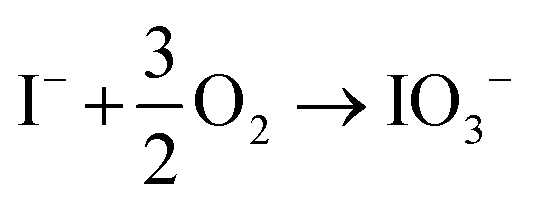 | (1) |
This iodate species transforms the surface PbI2 to a more thermodynamically favorable one, referred to as Pb(IO3)2*, in two steps, reactions (2) and (3).59
| PbI2* + 3O2 → Pb(IO3)2* | (2) |
| Pb(IO3)2* → Pb(IO3)2 + VPbI2 | (3) |
Importantly, the ultrathin ALD layer also benefits device performances and long-term stability. The current density–voltage curves (J–V curves) of the uncoated and ALD-0.75nm PSCs are depicted in Fig. 6a. A champion efficiency of 20.5% (19.1%) was achieved for ALD-0.75nm (uncoated) devices. Fig. S19 (ESI†) shows the statistics collected from 12 cells, respectively (refer to Table S1 for detailed photovoltaic parameters in the ESI†). The average short-circuit current density (JSC) of the uncoated and ALD-0.75nm samples was unaffected and consistent with the external quantum efficiency (EQE) of the devices shown in Fig. S20 (ESI†).
 | ||
| Fig. 6 (a) Champion J–V curves of the uncoated and ALD-0.75nm devices. The detailed parameters are listed in Table S1 (ESI†). (b) Normalized to 1 at the maximum power point (MPP) after 180 days of shelf-aging, The PSCs were kept for 1000 min under ambient conditions (>50% R.H. and 298 K) under 100 mW cm−2 illumination and J–V measurements were performed every 10 min. (c) and (d): Long-term stability of ALD-0.75nm and control devices for ~2 months during outdoor MPPT measurements in Barcelona, Spain (41.50°N, 2.11°E). (c) Normalized power output (d) Normalized performance factor. Here, the performance factor is the ratio between the integral of total power produced vs. the integral of the total irradiance power on the device over one day. | ||
Another effect of the possible surface passivation is an improvement in the fill factor (FF) to ∼80% of the ALD-0.75 nm, representing a ∼3% absolute increment compared to the uncoated device. To further understand the electronic role of such an ultrathin ∼0.75 nm ALD layer on the surface defects, we collected a map of the surface photovoltage value (SPV) distribution for both films, as shown in Fig. S21 (ESI†). The heterogeneous distribution of the SPV for the uncoated film suggests a non-uniform charge carrier density due to either the varied stoichiometry or non-uniform defect distribution.69 Overall, the SPV value decreased from 65 mV with an RMS variation of 5 mV on the uncoated sample to 55 mV with an RMS deviation of 3 mV on the ALD-0.75nm. The decrease of the SPV could be the result of the passivation of surface defect states, indicating improved homogeneity of the charge carriers and minimized surface defects.11
Furthermore, we have also performed electrochemical impedance spectroscopy (EIS) of uncoated and ALD-0.75nm devices. The impedance characteristics of the PSC presented in Nyquist plots show two semicircles in two distinct frequency regions, which represent different processes in the device, shown in Fig. S22 (ESI†).70 In the EIS response of the devices, the bulk recombination resistance (R2) is comparable with 3.0 kΩ and 3.2 kΩ for the ALD-0.75nm and uncoated devices, respectively. However, the interface recombination resistance (R3) increases from 2.3 kΩ for the uncoated device to 4.6 kΩ for the ALD-0.75nm device, indicating reduced recombination events at the interface. This is also consistent with the increase in the observed FF and VOC of the ALD-0.75nm PSCs. The fitting parameters are shown in Table S2 (ESI†).
Fig. S23 (ESI†) indicates that the long-term shelf-stability of the unencapsulated ALD-0.75nm device can retain up to 85% of its initial power conversion efficiency (PCE) after 180 days of storage in an N2 environment (<10% R.H.) while the ALD-uncoated PSCs shows a 30% drop in the PCE. To intensify the impact of intense light and atmospheric degradation on the PSCs, these 180-day shelf-aged uncoated and ALD-0.75nm devices underwent MPPT aging in ambient atmosphere (>50% R.H.) for 1000 min, shown in Fig. 6b. All the derived photovoltaic parameters exhibited a more rapid decrease for the uncoated PSCs, as illustrated in Fig. S24 (ESI†). It is crucial to note that understanding the underlying reasons for performance degradation requires analysis of the final device performance and also other photovoltaic parameters (such as JSC, VOC, and FF). Therefore, we extracted the final J–V from each MPPT measurement point and plotted it in Fig. S25 (ESI†). Losses in FF and JSC emerged as the dominant factors contributing to the decrease in the PCE of the uncoated devices. A significant improvement was observed in the ALD-0.75nm devices, maintaining up to 75% of the PCE before MPPT, along with comparatively stable VOC and FF. It is evident that in both cases, the decrease in the final device performance of the PSCs is a function of JSC and FF, and it declines for the uncoated PSCs.
As a figure of merit for greater device improvements, we performed outdoor device stability for the ALD-0.75nm vs. uncoated PSCs as per the ISOS-O-2 protocol in Barcelona, Spain (41.50°N, 2.11°E). Fig. 6c shows the normalized power output during the day and night cycles. The control device exhibits an exponential decline after 500 h, while the ALD-0.75nm device is stable until 1500 h, maintaining close to 98% of its initial PCE. To improve the outdoor comparison, we show the normalized performance factor (PF) of our devices in Fig. 6d, which is the ratio between the power produced and expected over one day, as used by Abate et al.71 Similar to the indoor MPPT shown in Fig. 6b, the performance of the ALD-0.75nm PSCs remained stable until 1500 h, three times higher than that of the uncoated device. The sudden drop in the performance for both the cells at around 500 and 1000 h is due to poor incident irradiance (in that particular period) and, accordingly, temperature as well as R.H. change, see Fig. S26 (ESI†). Notwithstanding, we observed that the ALD-0.75nm device showed better recovery after rainy days compared to the control.
These results indicate that the degradation of PSCs stems not only from poor charge transfer to the adjacent charge transport layer but also from poor charge generation within the active perovskite layer after shelf-aging and MPPT. Finally, the analysis performed here shows that a systematic study of the effect of individual layers under light-aging stress under ambient conditions can reveal multiple mechanisms of device degradation. Thus, we can infer that the presence of a ∼0.75 nm thin layer of Al2O3 acts as a barrier, enhancing long-term stability under ambient conditions.
Conclusions
In summary, our study focused on the long-term stability of PSCs, specifically examining the interaction between the perovskite material and the organic charge transport layer. To address these stability issues, we introduced an ultrathin Al2O3 (alumina) layer deposited via ALD at room temperature, ensuring that the underlying perovskite remained undamaged. Our findings indicated that the alumina layer functions as a dual-purpose diffusion barrier (against degassing) in addition to preventing moisture ingress into the perovskite. First, using nanoscale c-AFM, we demonstrated that the alumina conformally coats to the perovskite layers. This enhanced the contact of spiro-OMeTAD with perovskite while also acting as a defect-mitigating passivation layer. This improved the performance and intrinsic stability of the perovskite material. Secondly, the alumina barrier served as a protective layer impeding ion migration from the degraded spiro-OMeTAD into the perovskite and vice versa. Using a combination of spectroscopy, diffraction, and microscopy techniques, we showed that the alumina prevented the amorphization of crystalline perovskite, thereby enhancing the final device stability under ambient conditions, even without encapsulation. This study contributes to a holistic understanding of decoupling the final device degradation from the instability caused by ion migration from the perovskite material and by the residues from the degraded charge extraction layer into the perovskite. Hence, our study highlights the efficacy of a conformal diffusion barrier layer using an ultrathin alumina layer, deposited from ALD, in accelerating the commercialization and long-term durability of perovskite photovoltaics.Experimental section
Materials
N,N-Dimethylformamide (DMF, 99.8%), dimethyl sulfoxide (DMSO, 99.9%), spiro-OMeTAD, 4-tert-butylpyridine (TBP), chlorobenzene (CB), lithium bis (trifluoromethylsulfonyl) imide salt (Li-TFSI), and cesium iodide (CsI, 99.9%) were purchased from Sigma-Aldrich Co., Ltd. Lead(II) iodide (PbI2, 99.999%) and lead(II) bromide (PbBr2, 99.999%) were purchased from TCI Chemical. Formamidinium iodide (FAI, 99.9%) and methylammonium bromide (MABr, 99.9%) were purchased from GreatCell Solar. The SnO2 colloidal precursor (tin(IV) oxide, 15% in H2O colloidal dispersion) was purchased from Alfa Aesar. All salts and solvents were used as received without further purification.Perovskite solutions preparation
The SnO2 solution was prepared outside the glovebox by mixing 1 mL of SnO2 colloidal precursor with 3 mL of deionized water. The prepared solution was mixed using a vortex shaker for 60 s before use. The perovskite precursor and spiro-OMeTAD solutions were prepared in a nitrogen-filled glovebox. The perovskite solution was prepared by dissolving FAI (1.16 M), MABr (0.24 M), PbI2 (1.19 M), and PbBr2 (0.24 M) in a solvent mixture of DMF and DMSO in a 4![[thin space (1/6-em)]](https://www.rsc.org/images/entities/char_2009.gif) :1 volume ratio. This “mixed” solution was stirred for 300 s until complete dissolution. A 1.5 M stock solution of CsI prepared in anhydrous DMSO was added to the “mixed” solution and filtered with a 0.25 μm PTFE filter to obtain the CsMAFA triple-cation, Cs0.05(MA0.17FA0.83)0.95Pb(I0.83Br0.17)3. For the spiro-OMeTAD solution, 72.3 mg spiro-OMeTAD was dissolved in 1 mL chlorobenzene along, 28.8 μL 4-tert-butylpyridine (TBP) and 17.5 μL bis(trifluoromethylsulfonyl)imide lithium salt (Li-TFSI) solution (520 mg mL−1 in acetonitrile). After constant stirring, the solution was filtered before use.
:1 volume ratio. This “mixed” solution was stirred for 300 s until complete dissolution. A 1.5 M stock solution of CsI prepared in anhydrous DMSO was added to the “mixed” solution and filtered with a 0.25 μm PTFE filter to obtain the CsMAFA triple-cation, Cs0.05(MA0.17FA0.83)0.95Pb(I0.83Br0.17)3. For the spiro-OMeTAD solution, 72.3 mg spiro-OMeTAD was dissolved in 1 mL chlorobenzene along, 28.8 μL 4-tert-butylpyridine (TBP) and 17.5 μL bis(trifluoromethylsulfonyl)imide lithium salt (Li-TFSI) solution (520 mg mL−1 in acetonitrile). After constant stirring, the solution was filtered before use.
Device fabrication
Pre-patterned ITO substrates were cleaned sequentially with a detergent solution (2% Hellmanex in DI water), deionized water, acetone, and isopropanol for 15 min in an ultrasonic bath. After drying, the substrates were cleaned with ultraviolet ozone (UVO) for 15 min to remove organic residues. Next, the SnO2 solution was spin-coated onto the cleaned ITO substrates at 3000 rpm for 30 s, followed by annealing at 150 °C for 30 min. The SnO2 films were further cleaned by UVO treatment for 20 min and immediately transferred to the glovebox. The triple-cation perovskite precursor was spin-coated on the SnO2/ITO substrates at 1000 rpm for 10 s and 5000 rpm for 20 s. 150 μL of chlorobenzene was dropped at the last 5 s as an antisolvent. The substrate was then annealed at 100 °C for 30 min and allowed to cool before the next step. The samples were removed from the glovebox and transferred to the ALD system for Al2O3 deposition. After the ALD deposition, the samples were loaded in the glovebox again to deposit a spiro-OMeTAD layer at 4000 rpm for 20 s. Finally, gold was deposited using a 0.16 cm2 area at a rate of 0.5 Å s−1.Atomic layer deposition of Al2O3
Atomic layer deposition was carried out in an SI PEALD system (SENTECH Instruments GmbH). The reactor walls and substrate heater were maintained at room temperature (RT). Trimethylaluminum (TMA, Dockweiler Chemicals, Electronic Grade) and water (VWR International, M-Clarity™ = MQ1000) were used as the aluminium and oxygen sources, respectively. Both chemicals were kept in stainless steel bubblers at room temperature. Nitrogen (99.9999) was used as carrier gas with 120 sccm for both TMA and H2O. The ALD cycle of Al2O3 comprises a 60 ms pulse of TMA, a 15 s N2 purge pulse, a 60 ms H2O pulse, and a 15 s N2 purge step. During deposition, the substrate temperatures of both processes were fixed at 25 °C. The perovskite samples were placed directly on an aluminum carrier, with a silicon reference piece in its vicinity. The film thickness was measured post-deposition on a silicon reference piece using a SENTECH spectroscopic ellipsometer SE 800. To assess the film thickness, a refractive index of 632.8 nm of 1.64 was assumed while applying the Cauchy model. To achieve a film thickness of ∼0.75 nm, 14 ALD cycles were deployed, resulting in a growth rate of approximately 0.5 Å per cycle. For in situ ellipsometry, the total stack thickness consists of ∼471 nm of perovskite and ∼160 nm of ITO substrate plus silicate glass. Thus, the starting thickness reported was ∼666.5 nm, including an average roughness of ∼35.5 nm.JV and EIS measurements
The J–V characteristics of the solar cells were recorded in an ambient atmosphere under an AM 1.5 G, 100 mW cm−2 spectrum (WAVELABS, SINUS-70) using a Keithley 2400 source meter. The solar cells were unencapsulated during the test and measured in both forward and reverse directions using a 0.089 cm2 mask from −0.2 V to 1.2 V with 200 mV s−1 after 1 week of complete device fabrication. Impedance spectroscopy measures were performed using an Autolab potentiostat GSTT302N at short-circuit conditions with 10 mV AC voltage under dark in the frequency range of 0.01 Hz and 100 kHz.MPPT tracking- long-term stability
For this measurement, a class AAA continuous solar simulator with a spatial uniformity in irradiance greater than 2% over the entire test area (156 mm × 156 mm) was used under an irradiance of 100 mW cm−2 with an AM1.5G spectrum, and the samples were placed on a controlled metal table at a temperature of (25 ± 1) °C. An InfinityPV source measurement unit (SMU) was used to measure the IV curve and perform light-soaking degradation under MPPT conditions.MPPT tracking- outdoor stability
Encapsulation sealing was performed using glass-to-glass sealing. First, the active area was covered with a UV-curing epoxy and then the top glass was placed and exposed to a UV light source (254 nm) for 45 min, and then copper wires were connected to the back contacts using conductive silver epoxy.Outdoor stability (ISOS-O-2) tests were performed in Barcelona, Spain (41.30°N, 2.09°W, Csa climate). PSCs were mounted on a dual-axis sun tracker and performance was measured at MPP using an MP0205M24, LPVO maximum power point tracker. The solar intensity was measured with ISO 9060/IEC 61724 Class A pyranometers while the temperature was recorded using RK330-01 Atmospheric Temperature, Humidity & Pressure Sensors. All sensors were mounted on the same platform as the PSCs.
To calculate the performance factor, the output power density (Pout) from the device is integrated over a time interval of 1 day, and divided by the integrated input power density (Pin) from the measured solar irradiance over the same time of measurement. This is summarized in the following equation:

Electroluminescence (EL)
Electroluminescence (EL) images were captured using a silicon-based CCD camera (Hamamatsu ORCA-R2) without adding any additional optical filter to the lens. The electrical biasing of the samples under test has been conducted by using a digital DC Power Supply (Agilent E3642A)EQE
The external quantum efficiency (EQE) of the solar cells was measured using an Enlitech QE-R system.SEM
Surface topology images were obtained using a Hitachi S-4700 scanning electron microscope (SEM).XRD
The XRD patterns were measured on an X′′Pert Pro (PANanalytical) in Bragg–Brentano geometry using Cu Kα1 radiation (λ = 1.5406 Å) and scanning from 2° to 60° (2θ) with a step interval of 0.0167°.UV-vis
The absorption spectra were measured using a UV-Vis-NIR spectrophotometer (PERKIN ELMER, Lambda 1300).XPS
Near-ambient-pressure (NAP) XPS measurements were performed on a custom-built spectrometer (Specs) using a DeviSim NAP reactor cell coupled with a differentially pumped hemispherical electron energy analyzer (Phoibos 150 NAP 2D-DLD) and Al Kα X-ray source (μ-Focus 600). The samples were transferred to the NAP cell via ultra-high vacuum chambers with a base pressure of 1 × 10⁻⁹ mbar. During measurements, the samples were situated at a distance of 0.3 mm from an electron-collecting nozzle having an orifice diameter of 0.3 mm. The NAP cell operated in a dynamic mode with a completely open pumping outlet, while the required gas pressure was set using a proper gas inlet flow. Pure O2 (Linde, purity 99.999%) and H2O purified by several freeze–pump–thaw cycles were used in accelerated aging tests.REELS is performed in an ESCALAB-150Xi (Thermo Fisher Scientific) with an electron beam source of 50 eV, both with a pass energy of 10 eV in a UHV environment below 10−8 Torr.
Conductive AFM/SPV
Conductive AFM and SPV measurements were performed using an MFP-3D infinity atomic force microscope (Asylum Research, Oxford Instruments) in a nitrogen-filled glove box, where the humidity and oxygen levels were below 0.4% and 0.1%, respectively. The measurements were performed with platinum-iridium coated SCM PIT-V2 cantilevers (Bruker) with spring constants of 2 mN nm−1 and a free resonance of 75 kHz. The cantilever holder for the conductive AFM measurement was an ORCA cantilever holder from Asylum Research with a current amplification factor of 2 nA N−1.The AlOx coverage was obtained using Gwyddion software. A mask on the current map by setting a data range as a percentage was set the maximum value of 100% was appointed and determined the minimum value by checking the covered area. Finally, we chose the lowest possible minimum range that covers the high-current areas but not the entire current map.
For surface photovoltage (SPV) measurements, the sample was illuminated by a pulsed laser (Cobolt 06-01 Series) at 488 nm from below. Laser power was regulated by custom-written code embedded within the MFP3D control software by the AFM controller (Asylum Research ARC2), which supplied an analog voltage to activate the illumination. Surface photovoltage values were derived by subtracting the dark surface potential from the light surface potential.
TEM
For transmission electron microscopy (TEM), a lamella was prepared using the lift-out technique with a focused ion beam. The preparation was performed using a Zeiss Auriga Crossbeam Workstation. After selecting the area of interest, a protective platinum layer was deposited on the sample surface to protect the material near the surface from damage during the preparation. Then, the material was removed on both sides of the platinum layer using a gallium ion beam. The beam current of the gallium ions was reduced with a reduced thickness of the remaining material to avoid damaging the area of interest. When the lamella had a remaining thickness of approximately 1 μm, it was cut loose and transferred to a TEM Grid with the aid of a micromanipulator. On the grid, the final thinning to electron transparency (typically less than 100 nm in thickness) was performed. The prepared lamella had a width of 16 μm and a height of 8 μm.The TEM investigations were carried out in a Thermo Fisher Spectra 300 at 300 kV by bright-field imaging and selected area diffraction (SAD). The TEM was equipped with a high-brightness Schottky field-emission gun (X-FEG). The chemical composition was determined by spot measurements using energy-dispersive X-ray analysis (EDX). The TEM was equipped with a ThermoFisher Super-X EDX detector. The measurements were quantified using Velox software version 3.11. In addition, elemental distribution maps were recorded in the scanning TEM (STEM) mode with a pixel size of 150 pm and a dwell time of 4 μs.
ToF-SIMS
Time-of-flight secondary ion mass spectrometry was performed using a ToF-SIMS5 from Iontof. In addition to analyzing the Bi source, we chose a Cs source for sputtering. With this source, we have the opportunity to detect electropositive and electronegative elements simultaneously by selecting CsClusters, such as CsPb+, CsSn+, or CsI+. Furthermore, the Cs cluster shows a reduced matrix effect compared to single Ions as Pb+ or Sn+. The analyzed area was in the size 20 × 20 μm2, the sputter crater of the Cs source in the size of 300 × 300 μm2.Data availability
The data will be available upon reasonable request.Conflicts of interest
There are no conflicts to declare.Acknowledgements
M. S., M. K., and C. D. thank Helmholtz Young Investigator Group FRONTRUNNER. M. S., Y. Y., and S. W. thank the German Research Foundation (DFG) for funding (SPP2196, 431314977/GRK 2642). M. S. and M. L. C. acknowledge the funding from ProperPhotoMile. Project ProperPhotoMile is supported under the umbrella of SOLARERA.NET co-funded by The Spanish Ministry of Science and Education and the AEI under Project PCI2020-112185 and CDTI Project IDI-20210171; the Federal Ministry for Economic Affairs and Energy based on a decision by the German Bundestag Projects FKZ 03EE1070B and FKZ 03EE1070A and the Israel Ministry of Energy with Project 220-11-031. SOLAR-ERA.NET is supported by the European Commission with the EU Framework Programme for Research and Innovation HORIZON 2020 (Cofund ERA-NET action number 786483), funded by the European Union. M. S. acknowledges funding from the European Research Council under the Horizon Europe Program (LOCAL-HEAT, Grant Agreement 101041809). M. S. acknowledges funding from the German Bundesministerium für Bildung and Forschung (BMBF), project “NETPEC” (01LS2103E). M. S. also acknowledges funding by the Deutsche Forschungsgemeinschaft (German Research Foundation) via the project “Correlating Defect Densities with Recombination Losses in Halide-Perovskite Solar Cells.” The authors gratefully acknowledge the core facility SRF AMICA (Stuttgart Research Focus Advanced Materials Innovation and Characterization) at the University of Stuttgart for their support and assistance. This research was supported by the German Research Foundation (DFG, AOBJ: 661806). M. Kot and P. P. acknowledge the funding from Zentrales Innovationsprogramm Mittelstand (ZIM), Federal Ministry of Economics and Climate Protection Project no KK5087602BR1. M. S., M. K., and C. D. acknowledge the CERIC-ERIC Consortium for access to experimental facilities and financial support (proposal number 20232163). P. M. is grateful for the partial financial support provided by the Czech Ministry of Education, Youth and Sports (project LM2023072). M. K. and M. S. also acknowledge the VIPERLAB project financed by the European Union's Horizon 2020 (grant agreement No. 101006715). M. K. thanks Eugenia Zugasti and Javier Diaz Berrade from CENER, Spain, for their assistance during the MPPT measurements. M. K. also acknowledges Ludwig Marth from SENTECH for technical assistance during ALD deposition.References
- Best Research-Cell Efficiency Chart | Photovoltaic Research | NREL, 2023, Available from: https://www.nrel.gov/pv/interactive-cell-efficiency.html.
- J. Zhou, L. Tan, Y. Liu, H. Li, X. Liu and M. Li, et al., Highly efficient and stable perovskite solar cells via a multifunctional hole transporting material, Joule, 2024, 8(6), 1691–1706 CAS.
- L. Duan, D. Walter, N. Chang, J. Bullock, D. Kang and S. P. Phang, et al., Stability challenges for the commercialization of perovskite–silicon tandem solar cells, Nat. Rev. Mater., 2023, 8(4), 261–281 CrossRef CAS.
- M. V. Khenkin, E. A. Katz, A. Abate, G. Bardizza, J. J. Berry and C. Brabec, et al., Consensus statement for stability assessment and reporting for perovskite photovoltaics based on ISOS procedures, Nat. Energy, 2020, 5(1), 35–49 CrossRef.
- F. Li, X. Deng, F. Qi, Z. Li, D. Liu and D. Shen, et al., Regulating Surface Termination for Efficient Inverted Perovskite Solar Cells with Greater Than 23% Efficiency, J. Am. Chem. Soc., 2020, 142(47), 20134–20142, DOI:10.1021/jacs.0c09845.
- B. Chen, P. N. Rudd, S. Yang, Y. Yuan and J. Huang, Imperfections and their passivation in halide perovskite solar cells, Chem. Soc. Rev., 2019, 48(14), 3842–3867 RSC.
- C. Das, R. Roy, M. Kedia, M. Kot, W. Zuo and R. Félix, et al., Unraveling the Role of Perovskite in Buried Interface Passivation, ACS Appl. Mater. Interfaces, 2023, 15(48), 56500–56510, DOI:10.1021/acsami.3c13085.
- E. A. Alharbi, A. Y. Alyamani, D. J. Kubicki, A. R. Uhl, B. J. Walder and A. Q. Alanazi, et al., Atomic-level passivation mechanism of ammonium salts enabling highly efficient perovskite solar cells, Nat. Commun., 2019, 10(1), 1–9 CAS.
- G. Wu, R. Liang, M. Ge, G. Sun, Y. Zhang and G. Xing, Surface Passivation Using 2D Perovskites toward Efficient and Stable Perovskite Solar Cells, Adv. Mater., 2022, 34(8), 2105635, DOI:10.1002/adma.202105635.
- E. Ochoa-Martinez, M. Ochoa, R. D. Ortuso, P. Ferdowsi, R. Carron and A. N. Tiwari, et al., Physical Passivation of Grain Boundaries and Defects in Perovskite Solar Cells by an Isolating Thin Polymer, ACS Energy Lett., 2021, 6(7), 2626–2634, DOI:10.1021/acsenergylett.1c01187.
- M. Kedia, M. Rai, H. Phirke, C. A. Aranda, C. Das and V. Chirvony, et al., Light Makes Right: Laser Polishing for Surface Modification of Perovskite Solar Cells, ACS Energy Lett., 2023, 8(6), 2603–2610, DOI:10.1021/acsenergylett.3c00469.
- M. Saliba and W. Zuo, Sandwiched between flat barriers, Science, 2025, 387(6738), 1040–1041, DOI:10.1126/science.adw1552.
- T. Huang, S. Tan, S. Nuryyeva, I. Yavuz, F. Babbe and Y. Zhao, et al., Performance-limiting formation dynamics in mixed-halide perovskites, Sci. Adv., 2021, 7(46), 1799, DOI:10.1126/sciadv.abj1799.
- S. Tan, I. Yavuz, M. H. Weber, T. Huang, C. H. Chen and R. Wang, et al., Shallow Iodine Defects Accelerate the Degradation of α-Phase Formamidinium Perovskite, Joule, 2020, 4(11), 2426–2442 CrossRef CAS.
- Z. Saki, M. M. Byranvand, N. Taghavinia, M. Kedia and M. Saliba, Solution-processed perovskite thin-films: the journey from lab- to large-scale solar cells, Energy Environ. Sci., 2021, 14(11), 5690–5722 CAS.
- F. Lee, S. Marcus, E. Shero, G. Wilk, J. Swerts and J. W. Maes, et al. Atomic Layer Deposition: An Enabling Technology for Microelectronic Device Manufacturing, in: 2007 IEEE/SEMI Advanced Semiconductor Manufacturing Conference (ASMC). IEEE; 2007. 359–365. https://ieeexplore.ieee.org/document/4259230/.
- M. Leskelä and M. Ritala, Atomic Layer Deposition Chemistry: Recent Developments and Future Challenges, Angew. Chem., Int. Ed., 2003, 42(45), 5548–5554, DOI:10.1002/anie.200301652.
- M. A. Hossain, K. T. Khoo, X. Cui, G. K. Poduval, T. Zhang and X. Li, et al., Atomic layer deposition enabling higher efficiency solar cells: A review, Nano Mater. Sci., 2020, 2(3), 204–226 CrossRef.
- X. Dong, X. Fang, M. Lv, B. Lin, S. Zhang and J. Ding, et al., Improvement of the humidity stability of organic–inorganic perovskite solar cells using ultrathin Al2O3 layers prepared by atomic layer deposition, J. Mater. Chem. A, 2015, 3(10), 5360–5367 CAS.
- D. Choudhury, G. Rajaraman and S. K. Sarkar, Self limiting atomic layer deposition of Al2O3 on perovskite surfaces: a reality?, Nanoscale, 2016, 8(14), 7459–7465 CAS.
- V. Zardetto, B. L. Williams, A. Perrotta, F. Di Giacomo, M. A. Verheijen and R. Andriessen, et al., Atomic layer deposition for perovskite solar cells: research status, opportunities and challenges, Sustainable Energy Fuels, 2017, 1(1), 30–55 CAS.
- R. Singh, S. Ghosh, A. S. Subbiah, N. Mahuli and S. K. Sarkar, ALD Al2O3 on hybrid perovskite solar cells: Unveiling the growth mechanism and long-term stability, Sol. Energy Mater. Sol. Cells, 2020, 205, 110289, DOI:10.1016/j.solmat.2019.110289.
- D. Koushik, W. J. H. Verhees, Y. Kuang, S. Veenstra, D. Zhang and M. A. Verheijen, et al., High-efficiency humidity-stable planar perovskite solar cells based on atomic layer architecture, Energy Environ. Sci., 2017, 10(1), 91–100 CAS.
- M. Kot, C. Das, Z. Wang, K. Henkel, Z. Rouissi and K. Wojciechowski, et al., Room-Temperature Atomic Layer Deposition of Al2O3: Impact on Efficiency, Stability and Surface Properties in Perovskite Solar Cells, ChemSusChem, 2016, 9(24), 3401–3406, DOI:10.1002/cssc.201601186.
- M. Kot, L. Kegelmann, C. Das, P. Kus, N. Tsud and I. Matolinova, et al., Room-Temperature Atomic-Layer-Deposited Al2O3 Improves the Efficiency of Perovskite Solar Cells over Time, ChemSusChem, 2018, 11(20), 3640–3648, DOI:10.1002/cssc.201801434.
- C. Das, M. Kot, T. Hellmann, C. Wittich, E. Mankel and I. Zimmermann, et al., Atomic Layer-Deposited Aluminum Oxide Hinders Iodide Migration and Stabilizes Perovskite Solar Cells, Cell Rep. Phys. Sci., 2020, 1(7), 100112 Search PubMed.
- M. Kot, K. Henkel, K. Müller, L. Kegelmann, S. Albrecht and N. Tsud, et al., Al2O3-Atomic Layer Deposited Films on CH3NH3PbI3: Intrinsic Defects and Passivation Mechanisms, Energy Technol., 2019, 7(11), 1900975, DOI:10.1002/ente.201900975.
- D. Koushik, F. Naziris, J. Melskens, A. Nusteling, V. Zardetto and H. Schut, et al., On the effect of atomic layer deposited Al2O3 on the environmental degradation of hybrid perovskite probed by positron annihilation spectroscopy, J. Mater. Chem. C, 2019, 7(18), 5275–5284 CAS.
- D. Koushik, L. Hazendonk, V. Zardetto, V. Vandalon, M. A. Verheijen and W. M. M. Kessels, et al., Chemical Analysis of the Interface between Hybrid Organic–Inorganic Perovskite and Atomic Layer Deposited Al2O3, ACS Appl. Mater. Interfaces, 2019, 11(5), 5526–5535, DOI:10.1021/acsami.8b18307.
- S. Wang, Z. Huang, X. Wang, Y. Li, M. Günther and S. Valenzuela, et al., Unveiling the Role of tBP-LiTFSI Complexes in Perovskite Solar Cells, J. Am. Chem. Soc., 2018, 140(48), 16720–16730, DOI:10.1021/jacs.8b09809.
- F. Lin, J. Luo, Y. Zhang, J. Zhu, H. A. Malik and Z. Wan, et al., Perovskite solar cells: Li–TFSI and t-BP-based chemical dopant engineering in spiro-OMeTAD, J. Mater. Chem. A, 2023, 11(6), 2544–2567 CAS.
- S. Ghosh, D. Pariari, T. Behera, P. P. Boix, N. Ganesh and S. Basak, et al., Buried Interface Passivation of Perovskite Solar Cells by Atomic Layer Deposition of Al2O3, ACS Energy Lett., 2023, 8(4), 2058–2065, DOI:10.1021/acsenergylett.3c00296.
- N. Rolston, B. L. Watson, C. D. Bailie, M. D. McGehee, J. P. Bastos and R. Gehlhaar, et al., Mechanical integrity of solution-processed perovskite solar cells, Extreme Mech. Lett., 2016, 9, 353–358 CrossRef.
- Q. Wang, N. Phung, D. Di Girolamo, P. Vivo and A. Abate, Enhancement in lifespan of halide perovskite solar cells, Energy Environ. Sci., 2019, 12(3), 865–886 RSC.
- M. Saliba, T. Matsui, J. Y. Seo, K. Domanski, J. P. Correa-Baena and M. K. Nazeeruddin, et al., Cesium-containing triple cation perovskite solar cells: improved stability, reproducibility and high efficiency, Energy Environ. Sci., 2016, 9(6), 1989–1997 RSC.
- K. Artuk, D. Turkay, M. D. Mensi, J. A. Steele, D. A. Jacobs and M. Othman, et al., A Universal Perovskite/C60 Interface Modification via Atomic Layer Deposited Aluminum Oxide for Perovskite Solar Cells and Perovskite–Silicon Tandems, Adv. Mater., 2024, 2311745, DOI:10.1002/adma.202311745.
- L. P. Riikka and V. Wilfried, Island growth as a growth mode in atomic layer deposition: A phenomenological model, J. Appl. Phys., 2004, 96(12), 7686–7695, DOI:10.1063/1.1810193.
- J. Gong, M. Adnani, B. T. Jones, Y. Xin, S. Wang and S. V. Patel, et al., Nanoscale Encapsulation of Hybrid Perovskites Using Hybrid Atomic Layer Deposition, J. Phys. Chem. Lett., 2022, 13(18), 4082–4089, DOI:10.1021/acs.jpclett.2c00862.
- S. M. Prokes, M. B. Katz and M. E. Twigg, Growth of crystalline Al2O3via thermal atomic layer deposition: Nanomaterial phase stabilization, APL Mater., 2014, 2(3), 32105 Search PubMed.
- V. Miikkulainen, M. Leskelä, M. Ritala and R. L. Puurunen, Crystallinity of inorganic films grown by atomic layer deposition: Overview and general trends, J. Appl. Phys., 2013, 113(2), 21301 Search PubMed.
- G. Tang, T. Wang, J. Cao, Z. Zhao, J. Song and P. Liu, et al., Highly stable and efficient perovskite solar cells passivated by a functional amorphous layer, J. Mater. Chem. A, 2021, 9(38), 21708–21715 CAS.
- F. Zhang, Q. Huang, J. Song, Y. Zhang, C. Ding and F. Liu, et al., Growth of Amorphous Passivation Layer Using Phenethylammonium Iodide for High-Performance Inverted Perovskite Solar Cells, Solar RRL, 2020, 4(2), 1900243, DOI:10.1002/solr.201900243.
- I. Costina and R. Franchy, Band gap of amorphous and well-ordered Al2O3 on Ni3Al(100), Appl. Phys. Lett., 2001, 78(26), 4139–4141 CrossRef CAS.
- R. Zhao, K. Zhang, J. Zhu, S. Xiao, W. Xiong and J. Wang, et al., Surface passivation of organometal halide perovskites by atomic layer deposition: an investigation of the mechanism of efficient inverted planar solar cells, Nanoscale Adv., 2021, 3(8), 2305–2315 CAS.
- Y. Kutes, Y. Zhou, J. L. Bosse, J. Steffes, N. P. Padture and B. D. Huey, Mapping the Photoresponse of CH3NH3PbI3 Hybrid Perovskite Thin Films at the Nanoscale, Nano Lett., 2016, 16(6), 3434–3441, DOI:10.1021/acs.nanolett.5b04157.
- S. Panigrahi, T. Calmeiro, M. J. Mendes, H. Águas, E. Fortunato and R. Martins, Observation of Grain Boundary Passivation and Charge Distribution in Perovskite Films Improved with Anti-solvent Treatment, J. Phys. Chem. C, 2022, 126(45), 19367–19375, DOI:10.1021/acs.jpcc.2c05055.
- N. Li, Y. Luo, Z. Chen, X. Niu, X. Zhang and J. Lu, et al., Microscopic Degradation in Formamidinium-Cesium Lead Iodide Perovskite Solar Cells under Operational Stressors, Joule, 2020, 4(8), 1743–1758 CAS.
- B. P. Finkenauer, Ma. K. Akriti and L. Dou, Degradation and Self-Healing in Perovskite Solar Cells, ACS Appl. Mater. Interfaces, 2022, 14(21), 24073–24088, DOI:10.1021/acsami.2c01925.
- Q. Sun, P. Fassl, D. Becker-Koch, A. Bausch, B. Rivkin, S. Bai, P. E. Hopkinson, H. J. Snaith and Y. Vaynzof, Role of Microstructure in Oxygen Induced Photodegradation of Methylammonium Lead Triiodide Perovskite Films, Adv. Energy Mater., 2017, 7(20), 1700977, DOI:10.1002/aenm.201700977.
- R. Azmi, S. Zhumagali, H. Bristow, S. Zhang, A. Yazmaciyan and A. R. Pininti, et al., Moisture-Resilient Perovskite Solar Cells for Enhanced Stability, Adv. Mater., 2023, 2211317, DOI:10.1002/adma.202211317.
- F. J. Ramos, T. Maindron, S. Béchu, A. Rebai, M. Frégnaux and M. Bouttemy, et al., Versatile perovskite solar cell encapsulation by low-temperature ALD-Al2O3 with long-term stability improvement, Sustainable Energy Fuels, 2018, 2(11), 2468–2479 CAS.
- D. Zhang, D. Li, Y. Hu, A. Mei and H. Han, Degradation pathways in perovskite solar cells and how to meet international standards, Commun. Mater., 2022, 3(1), 1–14 Search PubMed.
- T. Hellmann, C. Das, T. Abzieher, J. A. Schwenzer, M. Wussler and R. Dachauer, et al., The Electronic Structure of MAPI-Based Perovskite Solar Cells: Detailed Band Diagram Determination by Photoemission Spectroscopy Comparing Classical and Inverted Device Stacks, Adv. Energy Mater., 2020, 10(42), 2002129, DOI:10.1002/aenm.202002129.
- C. Das, M. Wussler, T. Hellmann, T. Mayer, I. Zimmermann and C. Maheu, et al., Surface, Interface, and Bulk Electronic and Chemical Properties of Complete Perovskite Solar Cells: Tapered Cross-Section Photoelectron Spectroscopy, a Novel Solution, ACS Appl. Mater. Interfaces, 2020, 12(36), 40949–40957, DOI:10.1021/acsami.0c11484.
- M. Wussler, T. Mayer, C. Das, E. Mankel, T. Hellmann and C. Prabowo, et al., Tapered Cross-Section Photoelectron Spectroscopy of State-of-the-Art Mixed Ion Perovskite Solar Cells: Band Bending Profile in the Dark, Photopotential Profile Under Open Circuit Illumination, and Band Diagram, Adv. Funct. Mater., 2020, 30(27), 1910679, DOI:10.1002/adfm.201910679.
- C. Das, M. Kedia, W. Zuo, C. Mortan, M. Kot and J. Ingo Flege, et al., Band Bending at Hole Transporting Layer-Perovskite Interfaces in n–i–p and in p–i–n Architecture, Solar RRL, 2022, 6(9), 2200348, DOI:10.1002/solr.202200348.
- F. M. Rombach, S. A. Haque and T. J. Macdonald, Lessons learned from spiro-OMeTAD and PTAA in perovskite solar cells, Energy Environ. Sci., 2021, 14(10), 5161–5190, 10.1039/D1EE02095A.
- D. Di Girolamo, N. Phung, F. U. Kosasih, F. Di Giacomo, F. Matteocci and J. A. Smith, et al., Ion Migration-Induced Amorphization and Phase Segregation as a Degradation Mechanism in Planar Perovskite Solar Cells, Adv. Energy Mater., 2020, 10(25), 2000310, DOI:10.1002/aenm.202000310.
- J. Hidalgo, W. Kaiser, Y. An, R. Li, Z. Oh and A. F. Castro-Méndez, et al., Synergistic Role of Water and Oxygen Leads to Degradation in Formamidinium-Based Halide Perovskites, J. Am. Chem. Soc., 2023, 145, 24549–24557, DOI:10.1021/jacs.3c05657.
- S. Sánchez, B. Carlsen, V. Škorjanc, N. Flores, P. Serafini and I. Mora-Seró, et al., Thermodynamic stability screening of IR-photonic processed multication halide perovskite thin films, J. Mater. Chem. A, 2021, 9(47), 26885–26895, 10.1039/D1TA05248A.
- B. Dou, L. M. Wheeler, J. A. Christians, D. T. Moore, S. P. Harvey and J. J. Berry, et al., Degradation of Highly Alloyed Metal Halide Perovskite Precursor Inks: Mechanism and Storage Solutions, ACS Energy Lett., 2018, 3(4), 979–985, DOI:10.1021/acsenergylett.8b00305.
- E. Choi, J. W. Lee, M. Anaya, A. Mirabelli, H. Shim and J. Strzalka, et al., Synergetic Effect of Aluminum Oxide and Organic Halide Salts on Two-Dimensional Perovskite Layer Formation and Stability Enhancement of Perovskite Solar Cells, Adv. Energy Mater., 2023, 13(39), 2301717, DOI:10.1002/aenm.202301717.
- D. A. Jacobs, C. M. Wolff, X. Y. Chin, K. Artuk, C. Ballif and Q. Jeangros, Lateral ion migration accelerates degradation in halide perovskite devices, Energy Environ. Sci., 2022, 15(12), 5324–5339, 10.1039/D2EE02330J.
- P. Kaienburg, P. Hartnagel, B. E. Pieters, J. Yu, D. Grabowski and Z. Liu, et al., How Contact Layers Control Shunting Losses from Pinholes in Thin-Film Solar Cells, J. Phys. Chem. C, 2018, 122(48), 27263–27272, DOI:10.1021/acs.jpcc.8b09400.
- Y. Jiang, S. C. Yang, Q. Jeangros, S. Pisoni, T. Moser and S. Buecheler, et al., Mitigation of Vacuum and Illumination-Induced Degradation in Perovskite Solar Cells by Structure Engineering, Joule, 2020, 4(5), 1087–1103, DOI:10.1016/j.joule.2020.03.017.
- M. H. Miah, M. B. Rahman, M. Nur-E-Alam, N. Das, N. B. Soin and S. F. W. M. Hatta, et al., Understanding the Degradation Factors, Mechanism and Initiatives for Highly Efficient Perovskite Solar Cells, ChemNanoMat, 2023, 9(3), e202200471, DOI:10.1002/cnma.202200471.
- J. Lin, M. Lai, L. Dou, C. S. Kley, H. Chen and F. Peng, et al., Thermochromic halide perovskite solar cells, Nat. Mater., 2018, 17(3), 261–267, DOI:10.1038/s41563-017-0006-0.
- S. Yi and J. H. Lee, Degenerate Lattice-Instability-Driven Amorphization under Compression in Metal Halide Perovskite CsPbI3, J. Phys. Chem. Lett., 2022, 13(40), 9449–9455, DOI:10.1021/acs.jpclett.2c02047.
- Y. Yalcinkaya, P. N. Rohrbeck, E. R. Schütz, A. Fakharuddin, L. Schmidt-Mende and S. A. L. Weber, Nanoscale Surface Photovoltage Spectroscopy, Adv. Opt. Mater., 2023, 2301318, DOI:10.1002/adom.202301318.
- A. Guerrero, J. Bisquert and G. Garcia-Belmonte, Impedance Spectroscopy of Metal Halide Perovskite Solar Cells from the Perspective of Equivalent Circuits, Chem. Rev., 2021, 121(23), 14430–14484, DOI:10.1021/acs.chemrev.1c00214.
- M. Khenkin, H. Köbler, M. Remec, R. Roy, U. Erdil and J. Li, et al., Light cycling as a key to understanding the outdoor behaviour of perovskite solar cells, Energy Environ. Sci., 2024, 17(2), 602–610, 10.1039/D3EE03508E.
Footnotes |
| † Electronic supplementary information (ESI) available. See DOI: https://doi.org/10.1039/d4ee05703a |
| ‡ Present Address: Faculty of Electronics, Photonics and Microsystems, Wroclaw University of Science and Technology, Janiszewskiego 11/17, Wroclaw 50-372, Poland. |
| This journal is © The Royal Society of Chemistry 2025 |