
 Open Access Article
 This Open Access Article is licensed under a
 Creative Commons Attribution 3.0 Unported Licence
Emerging strategies for the large-scale fabrication of perovskite solar modules: from design to process
Bochun
Kang
 a and
Feng
Yan
*ab
a and
Feng
Yan
*ab
aDepartment of Applied Physics, Research Center for Organic Electronics, The Hong Kong Polytechnic University, Hung Hom, Kowloon, Hong Kong, P. R. China
bResearch Institute of Intelligent Wearable Systems, The Hong Kong Polytechnic University, Hung Hom, Kowloon, Hong Kong SAR, P. R. China
First published on 18th March 2025
Abstract
Perovskite solar cells (PSCs), recognized as a promising third-generation thin-film photovoltaic technology, offer notable advantages including low-cost production, high power conversion efficiency, and tunable bandgap characteristics. Despite these advancements, scaling up PSCs to large-area perovskite solar modules (PSMs) presents substantial challenges. To overcome the obstacles, alternative deposition methods such as solution-based blade coating, slot-die coating, spray coating, inkjet printing, and screen printing, as well as solvent-free methods like chemical vapor deposition and physical vapor deposition, are being explored to eliminate film inhomogeneity and defects when applied to a larger area. These emerging strategies aim to enhance film quality, uniformity, and scalability, which are essential for large-area applications. This comprehensive review systematically summarizes the manufacturing status of PSMs from fundamental theoretical principles to practical applications in processing, discussing various deposition techniques, and simultaneously exploring strategies to enhance PSM performance in terms of solvent, additive and interface engineering. Additionally, it delves into the stability challenges faced by large-scale manufacturing of commercial products, analyzing and summarizing the latest scribing processing and encapsulation technologies, and providing prospects for module development.
 Bochun Kang | Bochun Kang joined Professor Yan's group in 2023 and is now pursuing his PhD degree in the Hong Kong Polytechnic University, Department of Applied Physics. His current research interests include scalable perovskite solar modules design and fabrication. |
 Feng Yan | Feng Yan is a Chair Professor at the Department of Applied Physics and the director of Research Center for Organic Electronics in the Hong Kong Polytechnic University. He received his PhD degree in Physics from Nanjing University. He worked at Engineering Department of Cambridge University in 2001 as a Research Associate and joined the Department of Applied Physics of The Hong Kong Polytechnic University in 2006. He is a Highly Cited Researcher identified by Clarivate from 2021 to 2024. He has research interests in organic electronics, thin-film transistors, biosensors, solar cells, 2D materials, and smart materials. |
Broader contextWith the onset of the fossil energy crisis, the efficient utilization of solar energy has become critically important. This has led to significant commercial and research investments in the photovoltaic industry. The promising third-generation photovoltaic solutions, perovskite solar cells, recognized, have garnered substantial attention and made significant advancements in recent years. Certified small-area perovskite solar cell efficiencies have reached 26.7%, rivaling those of silicon solar cells. To facilitate commercialization, developing stable and efficient large-scale perovskite solar modules remains a crucial challenge. The commonly used small-scale spin-coating method in laboratory settings is less effective for large-area applications due to uneven centripetal forces. This comprehensive review addresses the emerging strategies for the large-scale fabrication of perovskite solar modules. Large-area coating techniques primarily include liquid-phase deposition methods (meniscus coating and droplet spraying) and non-liquid-phase deposition methods (physical and chemical vapor deposition). Furthermore, device design, encapsulation, and stability testing of solar modules are essential steps on the path to commercialization. |
1. Introduction
Solar panels, as simple and efficient devices for converting renewable solar energy into electricity, have contributed to mitigating the depletion of traditional fossil fuels.1,2 From the client's perspective, the rapid and sustained demand for photovoltaics (PV), which is forecast to grow by over 30% over the next five years, which has further attracted substantial commercial investment in the scale production of solar cells. As of 2023, the global cumulative installed capacity has exceeded 1 TW-scale.3,4Perovskite solar cells (PSCs), as a promising third-generation thin-film photovoltaic technology, are considered one of the most potentially applicable photovoltaic technologies for the future due to their ease of fabrication, low cost, high power conversion efficiency, and tunable bandgap characteristics.5–8 Based on the photovoltaic effect, when photons with energy greater than the bandgap of perovskite are absorbed, excitons are generated.9,10 Due to the low exciton binding energy in the perovskite absorbing layer, excitons rapidly dissociate to form electron–hole pairs.11 Subsequently, electrons pass through an electron transport layer (ETL) composed of an n-type semiconductor with matched energy levels while holes diffuse across a hole transport layer (HTL) based on a p-type semiconductor in the opposite direction, generating a directed output current.9,10 Currently, PSCs have undergone rapid development at the laboratory scale. Over the past decades, the power conversion efficiency (PCE) record has been continuously broken, soaring swiftly from 3.8% to over 26%, nearing the record held by silicon solar cells.12,13
Typically, small-area PSCs are extensively studied to innovate while conserving materials. However, in terms of real-world PV applications and industry, the scaling up of PSCs is an irresistible trend. In practical applications, large-area PSCs may necessitate the integration of multiple sub-cells into large-area perovskite solar modules (PSMs). The built-in series-connection cells enhance the output voltage while effectively relieving substantial losses due to parasitic resistance arising from charge transport distances within the transparent electrodes.14 The majority of PSCs now being explored are based on the spin-coating approach, with effective areas in the range of 0.04–1 cm2.15,16 When attempting to adopt spin-coating for large-area perovskite production, the radial centrifugal force can severely affect the film quality and form films with severe nonlinear inhomogeneous thicknesses along the radial direction.17 These morphological defects are manifested as numerous ring-shaped pinholes in thinner regions and non-radiative recombination in thicker areas.18 Nevertheless, the PSMs' requirement for film uniformity, non-pinhole, and nice crystallographic properties are mandatory for the sake of the series circuit. This conflict has stimulated the emergence of new processes for scaling up. Since the first report of PSM by Carlo et al.19 in 2014, research groups worldwide have made significant progress, reaching up to 23.3%,20 in the development of scalable processes for large-area PSMs and film deposition over the past decade.
Currently, various strategies have been developed in two dominant technique routes, solution-based and solvent-free evaporation, for depositing high-quality large-area perovskite films. These include solution-based blade coating,21 slot-die coating,22 spray coating,23 inkjet printing,24 and screen printing,25 as well as solvent-free vapor-based chemical vapor deposition (CVD)26 and physical vapor deposition (PVD).27 In response to these blossoming technologies, strategies such as solvent engineering,28 interface engineering,29 and additive engineering,30etc. have been employed to enhance the crystallization, carriers transport laterally and vertically among every single subcell, thereby paving the way for achieving high photovoltaic performance in PSMs.
This review systematically summarizes and discusses PSMs fabricated via various deposition technologies. Beginning with fundamental principles, we focus on the captivating and beneficial progress in the production of high-efficiency large-area modules and explore strategies for enhancing PSM performance from the perspectives of auxiliary processes and microscale science. Furthermore, we analyze the challenges faced by the large-scale fabrication application of PSMs and propose potential development pathways for future modules.
2. Device configuration
2.1 Perovskite solar modules
The exploration of PSCs performance is typically conducted on individual cells with very small areas in labs, usually ranging from 0.04 to 1 cm2.15,16,31 As these small cells are poised for commercial applications, there is an inevitable trend towards scaling up to larger areas. However, when the effective area is increased, the efficiency often experiences a significant decline. This is primarily due to the increased carrier transport distance within the PSC device, resulting in more charge loss over this extended distance. Additionally, the increase in cell area leads to higher internal resistance, hindering the flow of current and reducing current output, thereby resulting in lower PCE.32,33 Therefore, in response to the challenges of scaling up laboratory-scale photovoltaic cells for commercial applications and to drive commercialization, researchers have begun to shift their focus towards the development and optimization of solar modules.Since the diverse applications and fabrication processes of different-sized PSC devices, there is an urgent need for a standardized classification criterion to categorize module sizes and mitigate conflicting comparisons. The National Renewable Energy Laboratory (NREL) has proposed a universally applicable standard for module size classification, which finds wide application in various photovoltaic technologies such as Si and cadmium telluride (CdTe) solar modules.34 In the champion photovoltaic module efficiency chart, NREL has classified modules larger than 200 cm2 into distinct categories. Modules ranging from 200 to 800 cm2 are designated as “submodules”, while those spanning 800 to 6500 cm2 fall under the classification of “modules”. Modules with an area between 6500 and 14![[thin space (1/6-em)]](https://www.rsc.org/images/entities/char_2009.gif) 000 cm2 are identified as “standard modules”, and modules exceeding 14000 cm2 are referred to as “large modules”. NREL has chosen to disregard modules smaller than 200 cm2 in their classification. Research findings indicate that large-scale modules are typically manufactured by commercial enterprises, whereas laboratory investigations predominantly focus on modules ranging from 10 to 100 cm2. However, NREL's classification framework still necessitates complementary information to present a comprehensive categorization of modules. Encouragingly, Green et al.35 have bridged this gap in their continually updated solar cell efficiency tables over three decades. They define modules ranging from 10 to 200 cm2 as “minimodules”, while modules smaller than 10 cm2 are referred to as “cells”. Over the years, outstanding performers have emerged in various fields, with some already transitioning to large-scale commercial production, which is a highly promising development. Table 1 provides a record of the outcomes from the different classification categories to date.
000 cm2 are identified as “standard modules”, and modules exceeding 14000 cm2 are referred to as “large modules”. NREL has chosen to disregard modules smaller than 200 cm2 in their classification. Research findings indicate that large-scale modules are typically manufactured by commercial enterprises, whereas laboratory investigations predominantly focus on modules ranging from 10 to 100 cm2. However, NREL's classification framework still necessitates complementary information to present a comprehensive categorization of modules. Encouragingly, Green et al.35 have bridged this gap in their continually updated solar cell efficiency tables over three decades. They define modules ranging from 10 to 200 cm2 as “minimodules”, while modules smaller than 10 cm2 are referred to as “cells”. Over the years, outstanding performers have emerged in various fields, with some already transitioning to large-scale commercial production, which is a highly promising development. Table 1 provides a record of the outcomes from the different classification categories to date.
| Size (cm2) | Combined criteria | PCE records (%) | Active area (cm2) | Year | Stability description | Contributors | Ref. |
|---|---|---|---|---|---|---|---|
| ≤1 | Small cells | 26.7 | 0.0519 | 2024 | Undisclosed | University of Science and Technology of China | 35 |
| 1–10 | Cells | ||||||
| 10–200 | Minimodules | 23.30 | 27.22 | 2024 | Decrease to 94.66% after 1000 h light soaking under room temperature | École Polytechnique Fédérale de Lausanne | 20 |
| 200–800 | Submodules | 20.6 | 215.53 | 2024 | Undisclosed | Korea Research Institute of Chemical Technology and Unitest | 36 |
| 800–6500 | Modules | 20.7 | 810 | 2024 | Pass IEC61215 | Wuxi Utmolight Technology | 37 |
| IEC61730 | |||||||
| 6500–14000 |
Standard modules | 18.4 | 7200 | 2024 | Undisclosed | Renshine Solar | 38 |
| >14000 |
Large modules | 19.04 | 20000 |
2024 | Undisclosed | Kunshan GCL Photoelectric Materials | 39 |
 | ||
| Fig. 1 (a) Architecture of the parallel PSMs.40 Copyright 2021, Wiley-VCH GmbH. (b) Metallic grids on parallel PSMs.43 Copyright 2021, American Association for the Advancement of Science. (c) P1–P2–P3 laser scribing on series PSMs. (d) The overall plane view and (e) the current flow path in the side view of the series PSMs.44 Copyright 2020, MDPI, Basel, Switzerland. | ||
In contrast, series-connected PSMs enhance the open-circuit voltage while maintaining a stable current, which thereby limit the total current passing through the TCO and enable a greater reduction of resistive losses. Consequently, the series connection is regarded as a more promising module industrialization strategy. Normally, series modularization for PSCs is commonly achieved through a built-in circuit established by a P1–P2–P3 scribing process. This can be rapidly accomplished within microseconds under laser irradiation.45 This approach shows advantageous for large-scale batch production. The three-step sequential laser scribing process, the P1–P2–P3 interconnection process, is employed to achieve the formation of multiple interconnected independent PSCs for constructing a PSM, as depicted in Fig. 2c–e. Initially, the P1 laser scribing step is performed on the indium tin oxide (ITO) layer deposited on the glass substrate, creating isolated ITO substrates. Subsequently, in the P2 step, the entire structure is selectively removed before the top electrode is deposited, allowing the interconnection of individual cells through the deposition of the top electrode, resulting in a series-connected structure. Disparate from P1, the energy requirement for P2 is much higher depending on the material and the increase in thickness. P3 removes the top electrode with the assistance of laser, creating a conductive pathway eventually. It is noteworthy that the three scribing lines are required to be kept in strict geometrical parallel, preventing cells failure and leakage caused by the cross.46 The distance from P1 to P3 (scribing lines included) called the ‘dead area’, which act as wires and does not make any contributions to the photoelectric effects. In contrast to the “dead zone”, the “active region” bears the responsibility for the entire power conversion process. These two zones together compose the aperture area. And the geometric fill factor (GFF), determined by the ratio of ‘active area’ and ‘aperture area’ is an essential parameter for describing the effectively utilized area of PSMs. GFF plays a pivotal role in PSMs, serving as a crucial determinant of the module's light utilization capacity and conversion efficiency per unit area. A higher GFF signifies an augmented capability of the module to harness sunlight effectively, thereby establishing a positive correlation with the reduction of ‘dead area’. Simultaneously, it represents a paramount objective pursued in the development of PSMs scribing techniques.44,47 Compared to traditional mask-based patterning, laser scribing technology has the capability to elevate the GFF from 50% to a stable level exceeding 90%.48,49

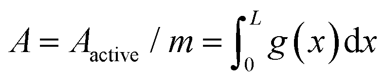
The initial work is to determine the shapes. It is known from the published paper that high-performance PSMs are typically designed in a rectangular configuration. Here, we will analyze the reasons behind this design through numerical analysis.50 Starting from the principle, under AM 1.5 solar illumination, the photovoltaic effect generates electron–hole pairs at each point distributed across the active area, resulting in a local current density. Subsequently, these electrons move vertically through the p–i–n junction and reach the top electrode edge to enter the series circuit loop as shown in Fig. 2c. Assuming that the subcell's length is the same as the module's length L, the area of every single subcell A can be illustrated as:
 | (1) |
| g(x) = (n + 1)Axn/Ln+1 | (2) |
The subsequent task behind is to ascertain the ideal number of subcells within the fixed module width W. We supposing that the module is divided into m subcells, the m − 1 scribings are required to complete the module fabrication. The total output power Pout within the module can be approximated as a compensation relationship between the power of a unscribed perfect device Pideal, Ploss and the scribing power loss Pscribing as follows:
 | (3) |
 | (4) |
Laser scribing is undoubtedly the most widely used technology in the module process. Functional materials can be vaporized through high-intensity lasers in an instant by absorbing laser photons.55–57 By taking advantage of the different absorption ranges of materials for wavelength, selective removal of materials can be achieved. Longer durations of laser pulses lead to higher energy output, resulting in a larger thermal impact zone. However, if the laser power is too high or the pulse frequency is not appropriate, it may lead to excessive damage to the perovskite layer or other functional layers, even causing burnout, thereby increasing the reject rate and lowering manufacturing yield. This also corresponds to higher process improvement costs. Generally, the smaller laser processing area in the PSMs, the larger GFF, indicating higher light utilization efficiency. Therefore, picosecond and femtosecond lasers have greater advantages compared to nanosecond lasers. Huang et al.57 performed dead area optimization, reducing the dead zone to 70 µm with the assistance of a picosecond laser, resulting in a GFF of 99%. Apart from laser scribing, another common scribing method is mechanical scribing.58 Unfortunately, mechanical scribing is a relatively unstable scribing process. During the P2 and P3 stages, excessive stress during mechanical scribing can cause damage to the bottom TCO, resulting in poor contact between the top metal electrode and TCO. This increases the series resistance of the device and leads to a decrease in the device's FF and GFF. Additionally, during the P3 stage, there is a risk of directly pressing the top metal electrode onto the TCO during mechanical scribing, which can result in a short circuit in the device. Unidirectional scribing can also lead to the accumulation of detached material at the trailing end along the direction of motion, causing serious defects. However, the energy saving of the mechanical one has also attracted the attention of the industry. For both scribing methods, the issue of electrode peeling after the P3 stage is unavoidable. The integrated dust removal functionalities have been developed to effectively alleviate this problem. Interestingly, it has been demonstrated that beyond the process itself, the design of scribing patterns can also enhance the performance of PSMs. Rakocevic and colleagues59 have innovatively designed a module with a point-contact configuration, achieving an enhancement in GFF from 95% to 99% as well. The record of GFF was broken by Carlo et al.,60 reaching a remarkable 99.6% improvement. They designed an unconventional discontinuous P2 pattern that miraculously reduced the dead area from a small size of 45 µm to an incredible limit of the average of 19.5 µm (Fig. 3a–c). And they proved the feasibility of a PCE of 20.7% on a miniature size of 2.6 cm2. Hence, the choice of the final commercial modularization process should be a decision that respects both production yield requirements and manufacturing costs. This is dependent on multiple constraining factors. For instance, opting for laser scribing implies substantial energy consumption, while enhancing precision using shorter pulse widths results in slower production efficiency.
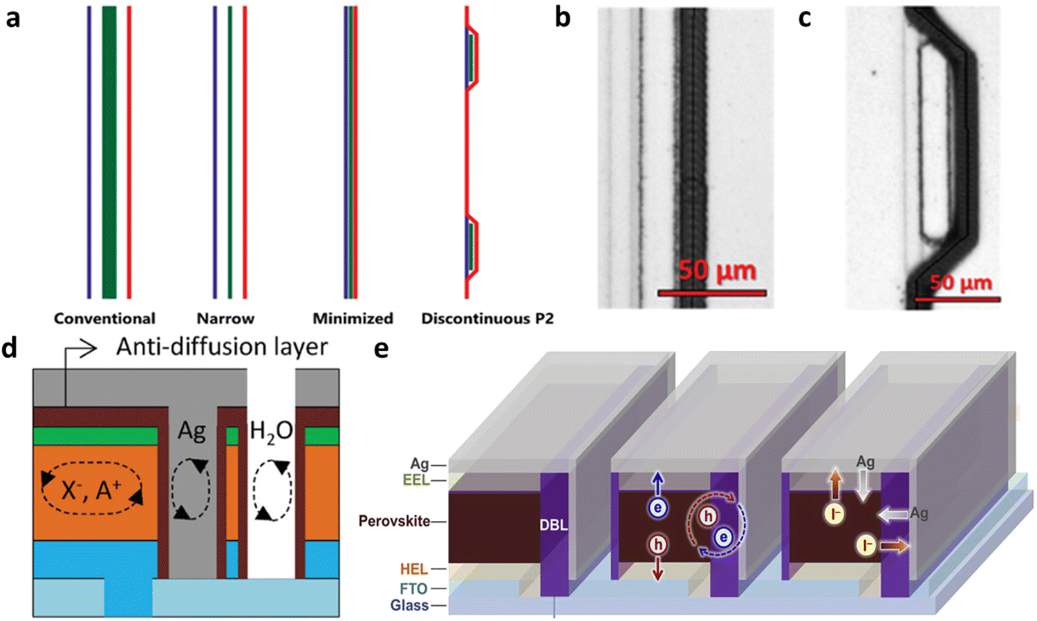 | ||
| Fig. 3 (a) Schematic diagram of conventional, narrow, minimized and discontinuous laser scribing designs. (b) Scanning electron microscope (SEM) figures of minimized and (c) discontinuous P2 interconnection.60 Copyright 2024, Wiley-VCH GmbH. (d) Anti-diffusion layer treated by O3.61 Copyright 2023, Wiley-VCH GmbH. (e) DBL for blocking lateral diffusion.62 Copyright 2019, Elsevier Inc. | ||
It is worth noting that the process inhomogeneities may have a negative impact on the PSMs in the cell-to-module fabrications. Especially in perovskite materials, their soft lattice structure makes them prone to deformation and aging. The presence of functional thin film defects in the layered structure of PSCs can lead to the exposure of the perovskite layer. When the perovskite material overflows or encounters the top electrode, irreversible reactions may occur, resulting in device damage. To address this issue, thin insulating layers such as bathocuproine (BCP)63 are used for longitudinal protection. These protective layers can be deposited above the perovskite layer, preventing its exposure to the external environment and thereby improving the device's lifespan. However, merely controlling the vertical diffusion is not sufficient to ensure the stability of PSMs. The severe lateral exposure in the cross-sectional area caused by laser scribing becomes a specific issue for PSMs. In the P2 and P3 layers, this leads to direct contact between perovskite materials and the external environment. Although subsequent encapsulation can isolate the environment, it cannot completely prevent stability losses caused by ion migration. Therefore, several efficacious strategies for lateral protection have been investigated. Mai et al.61 used ozone (O3) treatment to obtain PbOx at the cross-section, innovatively providing a solution to block lateral diffusion, while protecting P2 and P3, greatly reducing leakage caused by burrs generated by metal electrodes in laser scribing, and improving efficiency as shown in Fig. 3d. Additionally, low-dimensional diffusion barriers (DBL) were demonstrated by Han et al.62 as excellent lateral protection measures, increasing the potential barrier for ion diffusion as illustrated in Fig. 3e. The experiments illustrated that two-dimensional graphitic carbon nitride (g-C3N4) effectively inhibits the lateral migration of iodide by reducing it by a factor of 103–107. These modules achieved a stable PCE exceeding 15% for over 1000 hours under 85 °C.
2.2 Flexible/semitransparent solar modules
For catering to achieve broader commercial application scenarios such as building integrated photovoltaics (BIPV), researchers are developing a range of attractive module solutions, especially focusing on enhancing flexibility and transparency. The flexible PSMs (F-PSMs) are an emerging solar technology that has demonstrated a significant efficiency increase to 18.84%.64 A flexible substrate is a critical component of the F-PSM, providing a flexible support structure for the perovskite material. These substrates can be made of flexible plastics, films, or fiber materials, enabling the solar module to have characteristics such as lightweight, bendable, and customizable properties, usually polyethylene terephthalate (PET) and polyethylene naphthalate (PEN). However, the primary challenges of this technology involve designing efficient flexible electrodes and ensuring the bending stability of device structures and materials. From the perspective of large-scale production, flexible substrates often present challenges in achieving high-quality perovskite crystallization due to their relatively rough surfaces. During annealing, uneven thermal conduction and the presence of solvent trapped in substrate crevices in air-assisted coating processes can exacerbate this issue. The evaporation of retained solvent can lead to a significant number of defects at the grain boundaries.65 Gao et al.66 took inspiration from tendons and incorporated supramolecular poly(dimethylsiloxane) polyurethane materials with self-healing properties, resulting in a significant enhancement in the bending durability of F-PSMs. Even after undergoing 8000 bending cycles, the F-PSMs retained 80% of their initial efficiency. Meng et al.67 introduced glue-like poly(3,4-ethylenedioxythiophene):poly(ethylene-co-vinyl acetate) (PEDOT:EVA) as HTL, which lent its strong cohesion as shown in Fig. 4a to obtain 17.55% PCE on 31.20 cm2 and maintained 85% of the initial efficiency after 7000 mechanical bends. | ||
| Fig. 4 (a) Schematic diagram of PEDOT:EVA stress relief.67 (b) Transmittance changes with the amount of Br and the perovskite thickness.68 (c) Transparency effect under different laser patterns.69 (d) Schematic diagram of the large-scale R2R PSMs production process with the help of multi-process collaboration.70 | ||
Additionally, semi-transparent PSMs (ST-PSMs) are considered a significant research direction due to their effective photovoltaic conversion while maintaining high visible light transparency, meeting both architectural aesthetics and functional requirements. Since the light absorption capacity and photoelectric conversion capacity of perovskite are mutually restricted, how to balance PCE and average visible transmittance (AVT) becomes thought-worthy. In 2014, Eperon et al.71 first proposed semi-transparent PSCs, which triggered extensive subsequent research. Compared with traditional PSMs, the key technologies of ST-PSMs lie in the transparent top electrode and the preparation of high-quality semi-transparent perovskite films. Typically, transparent electrodes include TCO,72 ultra-thin metal electrodes,73 dielectric/metal/dielectric multilayer electrodes,74etc. Normally, the method for depositing the top transparent electrode is magnetron sputtering, but this technique frequently causes damage to the exposed substrate layer. To mitigate this Magliano et al.75 incorporated a vanadium oxide protective buffer layer, resulting in an efficiency of 15.7% over an area of 1 cm2, while preserving the AVT of 42%. The conductivity of these materials is generally lower than that of opaque materials, and they also lose the ability to reflect unabsorbed photons, allowing the perovskite layer to engage in secondary absorption. Another critical constraint on transparency is the composition and thickness of the perovskite. The size of the halide ions in the perovskite determines its bandgap; as the radius of the halide ions decreases, the bandgap of the perovskite widens, thereby increasing the visible light transmission region. Typically, an increase in bromide content leads to a noticeable enhancement in transparency. Additionally, employing diluted solvent concentrations to reduce the thickness of the perovskite layer can more effectively increase the AVT, as illustrated in Fig. 4b. Differently, a recent research proposed a method to achieve visual transparency without the conventional increase in AVT. This approach leverages the optical properties of human eyes. Yoo et al.69 utilized laser cutting to create micro-patterns with varying densities on the non-wavelength-selective PSMs. As shown in Fig. 4c, they achieved 32% AVT and 9.0% PCE over an aperture area of 4 cm2.
According to empirical investigations, diverse thin film coating processes exhibit disparate levels of selectivity and compatibility within distinct functional layers, each presenting unique merits and drawbacks. To facilitate expedited industrial manufacturing, the amalgamation of multiple technologies is imperative. For instance, realizing highly efficient and economically viable roll-to-roll (R2R) ideal production paradigms is a culmination of the synergistic integration of various methodologies. For example, Weerasinghe and colleagues70 achieved sustainable production of 11% efficient F-PSMs using an R2R process in an ambient environment. In this process, the ETL was applied using gravure printing, while the perovskite and HTL layers were coated through slot-die coating with air-knife assist. The top carbon electrode was coated using screen printing. As a trend for future development, this highly integrated mode, leveraging the strengths of each process (Fig. 4d), has led to breakthroughs in the final device, offering possibilities for the realization of rapid flow in industrial-scale production.
3. Large-scale perovskite deposition methods
3.1 Meniscus-based perovskite fabrication processes
 | (5) |
 | (6) |
 | (7) |
 | ||
| Fig. 5 (a) Schematic diagram of fluid dynamics of the meniscus coating process. (b) Schematics of the functions relationships between speed and perovskite thickness under evaporation and Landau–Levich regimes.80 (c) Measured film thickness h as a function of deposition speed v.79 Copyright 2009, American Chemical Society. | ||
 | (8) |
 | (9) |
 | (10) |
 | ||
| Fig. 6 (a) Plots for the relationship between crystallization free energy and particle radius. (b) Schematic illustration of the diffusion region around the spherical particle and (c) the plot of monomer concentration [M] as a function of distance x under reaction and diffusion-controlled situation. (d) Schematic diagrams of the chemical potential level shifts of particles with disparate size. (e) Plots of the relationship between the number of particles from nucleation to growth and σr of the size distribution.81 Copyright 2011, WILEY-VCH Verlag GmbH & Co. KGaA, Weinheim. | ||
This process remains closely related to the particle size and is primarily influenced by solubility. From a morphological perspective, both small and large particles reach the same size at the end of the growth period. This indicates that smaller particles have a higher growth rate. Theoretically, according to the Gibbs–Thomson relationship, when particles are too small, the chemical potential of their monomers is lower than that of the monomers in the solution. This favors the dissolution of solute particles in Ostwald ripening, leading to larger average crystalline sizes (Fig. 6d). The growth rate which is determined by radius r and time t can be expressed as:
 | (11) |
In the typical blade coating process, the precursors are dripped parallel to the doctor blade or the gap between the doctor blade and the glass, where it is spread uniformly using the liquid's surface tension. Subsequently, the blade moves relatively to the substrate and drags the solution onto the substrate to form a uniform film. Based on the fluid mechanics theory discussed at the beginning of this chapter, it has been determined that the coating speed and the distance between the blade and the substrate play decisive roles in the thickness of the film. However, when it comes to the quality and uniformity of crystallization, there is still a lack of quantitative control. Under constant velocity conditions, as the film coating progresses, the amount of perovskite precursor stored within the gap decreases. This significantly leads to uneven film thickness caused by meniscus deformation. In addition, the property of the content of precursor storage in blade gap can limit its development in terms of film expandability. In 2015, Tsai et al.96 proposed a coating method with constant acceleration, increasing the uniformity under the acceleration of 6 mm s−2 (Fig. 7a). For the same principle, uniformly accelerated variation of the distance of the blade head from the substrate may be a worthwhile option to explore for guiding high quality films. There are still no attempts in this process. In addition, higher speeds lead to severe viscous resistance exerted on the meniscus, resulting in higher solution consumption, thickness gradients along the coating direction, and prolonged drying time.79,97 Therefore, several strategies have been developed to reduce the viscosity of precursor solutions. The alteration of solvents can condition the viscosity, and Zhuang et al.21 adjusted the high-evaporation solvent ACN in the blade-coated bromide surface modifier and perovskite precursor (Fig. 7b), resulting in the preparation of PSCs with an efficiency exceeding 24%. Moreover, in 2018, Deng et al.30 introduced trace amounts of the surfactant L-α-phosphatidylcholine (LP) into the precursor solution. This approach modulated the fluid drying kinetics of the MAPbI3 precursor where MA is methylammonium and increased the adhesion of the perovskite ink to the underlying non-wetting charge transport layer. This strategy enabled them to achieve a PCE of around 15% with an effective area exceeding 50 cm2. LP subsequently emerged as a widely influential pre-additive surfactant. Furthermore, temperature and the volume of the added solution are also important controllable parameters. Arun et al.98 conducted temperature control on the doctor blade and explored the different effects of substrate temperature, solution volume, and speed parameters on the crystalline morphology (Fig. 7c and d). The early-stage process exploration of this system discovered that the size of perovskite islands increases with the increase in solution volume and substrate temperature. Overall, the effects of these parameters are based on the hydrodynamic tuning of the Levich–Landau regime, a quest to achieve an optimal balance between the equipment and the fluid flow characteristics.
 | ||
| Fig. 7 (a) Schematic diagram of bar coating with constant speed and constant acceleration.96 Copyright 2015, Elsevier B.V. All rights reserved. (b) SEM of surface reconstructed MA0.7FA0.3PbI3 perovskite film.21 (c) Schematics of the shrinkage of the ink droplet drying on a hydrophobic substrate without LP and (d) the pinning effect with LP.30 Copyright 2018, Springer Nature. (e) Plots of the perovskite island size variation with the solution volume and (f) substrate temperature.98 Copyright 2016, Elsevier. | ||
 | ||
| Fig. 8 (a) Schematic diagram of the slot-die coating equipment.99 Copyright 2024, Wiley-VCH GmbH. (b) Schematic diagram fluid mechanics models and core parameters in slot-die coating.103 Copyright 2016, American Institute of Chemical Engineers. (c) Images of slot-die coated perovskite thin films under different combination of ink supply rate and coating speed. From left to right: too fast, too slow and balanced supply.104 (d) The image and (e) schematic illustrations of ribbing defects during slot-die coating.99 Copyright 2024, Wiley-VCH GmbH. (f) Schematic diagram of slot die coating of perovskite films using 150 °C substrate-heating (left) and 150 °C substrate-heating/75 °C substrate-heating (right). (g) Color map of PCEs at the different head temperatures versus slot-die coating speeds. (h) Only-head heating with various temperatures.105 Copyright 2022, Elsevier B.V. | ||
From the perspective of process parameters, both slot-die coating and blade coating belong to the meniscus coating model, sharing fundamental process parameters. However, due to the slot-die mode, the precursor flow rate, or the injection rate, becomes an additional influential parameter in slot-die coating. Its matching with the motion speed of the slot-die is a key approach to addressing film formation defects. It is worth noting that it is a double-edged sword as it provides a more sustained solution supply, but the liquid reservoir in the slot-die introduces complex and unpredictable fluid changes in the meniscus. In this regard, Ding et al.103 systematically discussed the causes of defects in slot-die processes. They identified five defect formation mechanisms. Firstly, a too low solvent injection flow rate affects the minimum wet film thickness, leading to the rupture of the receding meniscus and the formation of an incomplete film (Fig. 8c). Additionally, imbalances in dynamic wetting, such as interruptions during the coating process, result in film discontinuity. The introduction of bubbles during liquid reservoir injection creates bubble-related voids within the wet film and uncoated areas of the substrate. Exceeding speed limitations causes ink to gradually accumulate on the coating head and leads to loss of pre-measured and expected film thickness. Lastly, the mismatch of vacuum pressure results in the appearance of ribbings (Fig. 8d and e). These four defects are all caused by variations in the advancing meniscus.99 In addition, they designed a different coating head to try to widen the machining window and eliminate defects caused by meniscus variations. In 2021, Zimmermann et al.106 explored a two-step sequential deposition process to achieve precise control over the porosity of lead-based intermediates for optimal perovskite conversion efficiency. They successfully obtained a uniform perovskite layer with an area of 5 × 10 cm2. Furthermore, they achieved an efficiency of 15.2% on an effective area of 12 cm2.
Similar to blade coating, slot-die coating also lacks the crystallization driving force inherent in traditional spin coating. Therefore, additional quenching assistance is necessary.107 The volatility rate of the solvent is crucial for the quality of perovskite thin films. Rapid solvent evaporation may result in defects in the film, such as pinholes or cracks, while slow solvent evaporation can lead to incomplete crystallization of the film, affecting device performance. The crystallization assistance process following film coating is discussed in detail in Section 3.1.5 including methods such as air-knife and fast-vacuum-assisted flash evaporation. Furthermore, the unique structural characteristics of slot-die coating allow for more intriguing approaches to crystallization assistance, such as utilizing the synergistic heating of the slot-die head and substrate to facilitate crystallization (Fig. 8f). This method effectively suppresses the coffee-ring effect and enhances crystallization quality. A temperature-adjustable slot-die head was designed by Seo et al.105 under the heating condition of 75 °C, together with the substrate environment of 150 °C (Fig. 8g), they used a one-step method to prepare PSCs with a PCE of 17.05%, which is an improvement of more than 15% compared to the control. However, it is important to note that when the temperature of the slot-die head exceeds 80 °C, solute precipitation at the outlet can obstruct the precursor flow in the ink reservoir. Their findings demonstrate that this strategy significantly enhances the controllability of nucleation. A more appropriate nucleation rate reduction provides sufficient time for the formation of larger grains. Notably, in the absence of hot substrate assistance, merely adjusting the temperature of the hot-head resulted in a significant performance degradation with increasing temperature (Fig. 8h). This is attributed to the negative temperature gradient from the outlet to the substrate, which reduces solvent evaporation and consequently diminishes the crystallization driving force.108 Despite the superior scalability of slot-die coating due to its continuous liquid supply design, the fine delivery tubes and complex feeding structures of this method increase the difficulty of equipment cleaning and maintenance. Additionally, the significant cost of consumables associated with daily laboratory use is also a noteworthy concern.
Among these options, the air-knife-assisted process has emerged as one of the most extensively employed techniques for accelerating solvent evaporation, primarily due to its instantaneous switching capability and exceptional control (Fig. 9a). Typically, inert gases such as nitrogen and argon are commonly employed in this process. The pioneer is the work by Huang et al.111 in 2014 introduced the utilization of gas-assisted crystallization on perovskite films. The fundamental principle underlying this strategy involves the direct removal of surplus solvents through the introduction of enhanced airflow, leveraging gas diffusion mechanisms.112,113 The net mass flow rate j, governs the evaporation process and can be determined using the following equation:
 | (12) |
 | (13) |
 | ||
| Fig. 9 (a) Schematic illustrations of air-knife assist, (b) vacuum assist and (c) in situ heat assist modes. (d) Schematics of main, side and top views of uneven evaporation during blade coating. (e) Schematic diagrams of the flow tracks of the Marangoni and capillary convective flows under meniscus coating process.114 | ||
Besides, vacuum assistance is also a fast and proficient solvent removal solution (Fig. 9b). By rapidly evacuating the chamber to a negative pressure state, the solvent can be quickly evaporated and dried within seconds. Guo et al.115,116 first introduced this technique in the meniscus process in 2019 and analyzed the reasons for the improvement in the filling factor from the perspective of crystallization kinetics control. In this flow, vacuum pumping rate and duration are two important factors affecting nucleation and crystallization, and their relationship is as follows:
| P = P0exp(−αt) + Plimit | (14) |
:6 between DMF and NEP, they achieved champion performance. They discovered that at this volume ratio, there was only a 1-second difference in nucleation rate during the cell-to-module scaling process, providing a surprisingly scalable solution. Ultimately, during the scaling process from 0.08 cm2 to 22.96 cm2, there was only approximately a 0.9% efficiency loss. This highlighted the tremendous commercial prospects of vacuum-assisted technology.
Another way of accelerating evaporation is the in situ heating (Fig. 9c). Initially, determining the thermal processing window is essential to achieve an equilibrium that prevents the excessive capillary flow from transporting solutes to the interface, forming coffee rings that disrupt homogeneity and morphology. In this context, it becomes necessary to consider a new fluid mechanics factor, the Marangoni effect (Fig. 9d and e).76,114 As the solvent evaporates during the coating process, the formation of temperature gradients causes the surface tension modification at the contact phase. The hot environment intensifies to a reverse Marangoni flow, offsetting capillary flow, to help mass transport from the edges towards the solution center. Here, the Marangoni number Ma is used to represent a dimensionless quantity that characterizes the relationship between surface tension and viscous forces. The relationship is as follows:
 | (15) |
In summary, the meniscus coating process and crystallization-assisted techniques in terms of processing to aid in understanding and obtaining more perfect crystal films have been developed. Additionally, innovative material engineering approaches that enhance performance through solvent and additive solutions in subsequent discussions were explored.
3.2 Droplets-based fabrication process
Controlled contact-free droplet splatting is a viable solution for large-area manufacturing in the fields of electronics, bioengineering and nanotechnology, etc. Disparate from the direct fluid coating, this approach utilizes a nozzle to disperse droplets, forming uniform functional films onto a substrate, thereby enabling customizable and scalable fabrication techniques.The outcome of this process is determined by the specifications of the nozzle (distance to substrate, speed, flow rate), the ink (viscosity, surface tension), and the substrate (temperature, wetting properties). From the perspective of theoretical physics models of the process, it is summarized as droplet impact dynamics (DID), within which, the factors mentioned above are quantified using three evaluation criteria for printing adaptability: Weber (We), Reynolds (Re), Ohnesorge (Oh) and Z. We and Re determine the relative importance of inertial forces compared to viscous effects and the ratio of inertial forces to capillary forces, respectively. Oh and Z refer to the dimensionless quantifications of the balance between viscous forces, inertial forces, and capillary forces, and are used to determine whether the ink can be sprayed stably. These can be expressed using the following equations:
 | (16) |
 | (17) |
 | (18) |
 | ||
| Fig. 10 (a) The processing parameter window for DID.120 Copyright 2023, Elsevier Ltd. (b) Schematic illustration of the spray coating and crystallization mechanism.121 (c) Schematic diagrams of pressure-assisted spray,122 (Copyright 2012, Elsevier B.V.) (d) sonication-assisted spray123 (Copyright 2023, Wiley-VCH GmbH) and (e) electrospray coating.124 (Copyright 2023, Wiley-VCH GmbH) (f) changes in the efficiency of PSCs of different sizes prepared by spray coating.125 (g) Schematics of CIJ and DOD inkjet printing methods.119 Copyright 2017, Wiley-VCH Verlag GmbH & Co. KGaA, Weinheim. | ||
Spray coating and inkjet printing are the most promising processing techniques in the field of PSMs that apply this underlying physical model. In this chapter, these two techniques will be discussed in detail.
In addition to the light-absorbing layer, Schackmar et al.131 developed all-functional-layer inkjet-printed PSCs using a full-functional layer. They conducted a step-by-step optimization of inks such as NiOx, phenyl-C61-butyric acid methyl ester (PC61BM), and BCP, as well as the specifications for nozzles and the substrate interface. The resulting PSCs achieved PCE of 17.2% and 12.3% for devices with areas of 0.11 cm2 and 1 cm2 respectively. Wei et al.132 investigated the feasibility of utilizing the passivating agent 2-adamantylamine hydrochloride (2-ADAHCl) through inkjet printing. By controlling the deposition surface density at 2.5 µg cm−2, they achieved a remarkable PCE of 24.57% in their PSC devices. Gao et al.133 have achieved large-area MAPbI3 perovskite solar cells based on full inkjet printing. They utilized PEN as the inkjet printing substrate and, following vapor annealing in ethyl acetate, obtained a dense and uniform morphology perovskite film over a sizable area of 120 cm2 with 16.78% milestone PCE.
The relatively slow processing speed of inkjet printing, compared to other large-area techniques, can be attributed to the smaller size of the nozzle. This may explain the limited number of published results regarding the successful application of inkjet printing in large-area PSMs research. Moreover, achieving synchronized crystallization at different positions during the printing process is a significant challenge, given the critical importance of timing for perovskite precursors. This complex crystallization kinetics problem greatly impacts the uniformity of the resulting films. Along with the high demand of the DID process on the quality of inks, the development of inks is an extremely important topic.
3.3 Contact pattern printing process
 | (19) |
:0.75 paste to dilutant ratio. Their study achieved an efficiency close to 9.9% on PSMs with an area of 224 cm2.
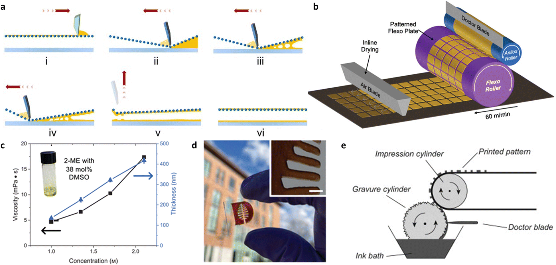 | ||
| Fig. 11 (a) Schematic diagram of screen printing: transfer of ink from the screen to the substrate.138 Copyright 2022, Springer Nature. (b) Schematic diagram of flexographic printing process. (c) Viscosity of perovskite ink (black line) and thickness of deposited perovskite film (blue line) as a function of lead concentration in the perovskite precursor. (d) Precise graphic printing by flexographic.141 Copyright 2023, Wiley-VCH GmbH. (e) Schematic diagram of gravure printing process.142 Copyright 2015, Elsevier Ltd. | ||
Overall, the excellent compatibility of screen printing enables the realization of large-area printing for the full functional layer of PSMs. Currently, it exhibits outstanding performance in processing high-viscosity inks within mesoporous carbon electrode device structures. Notably, in scalable production, how to clean the mesh poses a complex and costly issue compared to other processes.
Flexographic printing technology is widely used to produce transparent electrodes and interface layers in polymer and organic solar cells.143–145 It is considered to have great potential in customized flexible PSMs. However, currently, there is limited research and most of it focuses on non-absorb ink development, such as Poly(3,4-ethylenedioxythiophene) polystyrene sulfonate (PEDOT:PSS),146 NiOx,147etc. Thus far, the team of Scheideler and Huddy is the only one that has published their exploration of the flexographic process for perovskite ink (Fig. 11c and d).141 They successfully prepared MA0.6FA0.4PbI3 films with controlled thicknesses ranging from 100–500 nm under N2-assisted conditions. Also, their precise edge control resolved the challenge of uneven edges in the P2 scribing process. Ultimately, they achieved large-scale manufacturing on a 140 cm2 substrate and realized a champion PCE of 20.4% on a 0.134 cm2 PSC. Unfortunately, they did not continue the exploration of PSMs, but they have already paved a significant milestone in this area.
3.4 Solvent-free fabrication techniques
The solvent-free processing technique is an environmentally friendly method for manufacturing PSMs. In comparison to the traditional solvent-based process, it completely has no or minimal use of organic solvents. This method reduces the negative environmental impact by minimizing the emission of volatile organic compounds, thereby mitigating potential risks to air quality and human health. In general, solvent-free vapor deposition is an environmentally friendly large-area coating strategy that offers excellent reproducibility. It also allows for flexible control of patterns through the use of masks. Additionally, it enables the production of high-quality crystalline films with uniform and controllable thickness. Unfortunately, the energy consumption and equipment costs associated with high-vacuum and high-temperature environments are unavoidable drawbacks. However, despite these limitations, vapor deposition remains a highly promising and competitive large-area coating strategy with significant potential.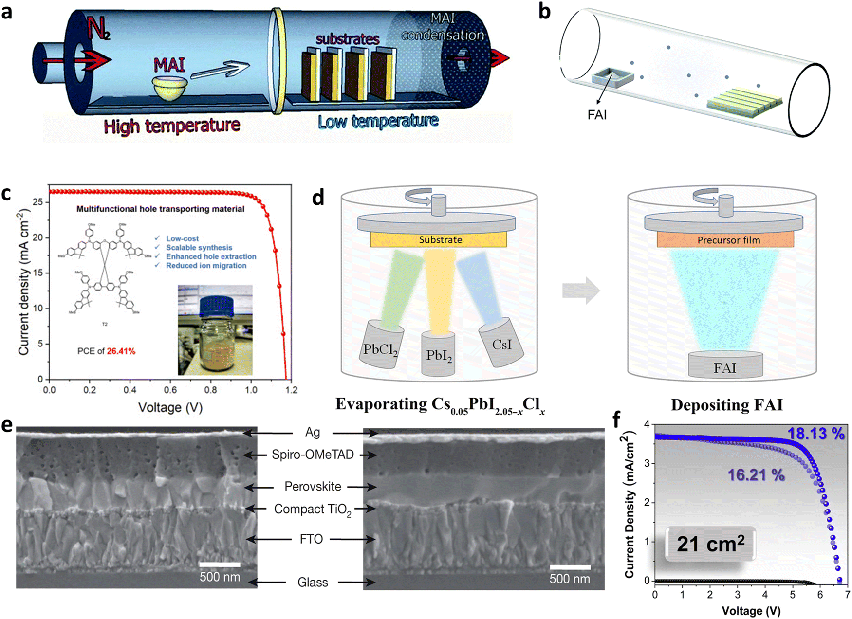 | ||
| Fig. 12 (a) Schematic diagram of the HCVD furnace and MAI deposition onto metal halide seeded substrates.156 (b) Hybrids-CVD of the FAI organic precursor for the formation of perovskite.48 (c) New HTL materials ‘T2’ assisted the PSCs to achieved a records PCE though co-evaporation.158 Copyright 2024, Elsevier Inc. (d) Simplified scheme presenting the Cl-containing alloy-mediated sequential vacuum deposition approach.159 (e) The cross-sectional SEM images of PSCs constructed from a vapor-deposited perovskite film (left) and a solution-processed perovskite film (right).160 Copyright 2013, Springer Nature Limited. (f) PCE has been enhanced to 18.13% on a 21 cm2 platform with co-evaporation.161 Copyright 2020, Elsevier Inc. | ||
:1 using CVD. This hybrid vapor deposition approach induced the formation of PbI2-DMSO intermediate phases at grain boundaries. Through recrystallization, a dense and low-defect CsxFA1−xPbI3−yBry light-absorbing layer is formed. This approach achieved a champion PCE of 19.9% on PSMs with an area of 10 cm2. More recently, Zhou et al.,158 as the holders of the efficiency record, fabricated high-quality FAPbI3 thin films by combining a dual-source two-step co-evaporation method (Fig. 12c), achieving a record-breaking certified efficiency of 26.21% on small-area devices and a PCE of 21.45% on a minimodule with an area of 14.4 cm2.
Through the comparison of the deposition processes of various large-area PSMs, we have summarized the differences between different techniques in Table 2 to aid in understanding the distinctions among them. Spin-coating consistently leads with the highest efficiency records; however, concerning scalability, a majority of high efficiency PSMs are generated through meniscus-based technologies and PVD. Despite their ability to provide high-quality thin films, CVD and PVD processes are constrained in high-throughput manufacturing due to their demanding processing environments and slower deposition rates. Droplets-based and pattern-based methods exhibit relatively lower efficiencies but possess the advantage of patterned manufacturing, suitable for specific application scenarios. Techniques such as flexographic and gravure printing have yet to witness successful PSM attempts, leaving room for further research in the future. Overall, we believe that blade coating and slot-die coating strike a balance between manufacturing efficiency and device performance, serving as robust tools for the industrialization of large-scale PSMs. Future process selections should weigh efficiency, material utilization, process speed, and environmental adaptability to drive the commercial application of PSMs.
| Perovskite deposition methods | Process type | Materials consumption | Cycle time | Environment requirement | PCE records of PSCs (%) | PCE records of PSMs (%) |
|---|---|---|---|---|---|---|
| Spin coating | Centrifugal | High | Medium | Glove box | 26.735 | 22.96163 |
| Blade coating | Meniscus-based | Low | Fast | Ambient, low humidity | 25.31164 | 23.320 |
| Slot-die coating | Meniscus-based | Low | Fast | Ambient, low humidity | 24.1165 | 21.9165 |
| Spray coating | Droplets-based | Low | Fast | Ambient, low humidity | 22.43166 | 18.0166 |
| Inkjet printing | Droplets-based | Low | Fast | Ambient, low humidity | 18.26167 | 16.78133 |
| Screen printing | Pattern-based | Low | Fast | Ambient, low humidity | 20.52138 | 18.12138 |
| Flexographic printing | Pattern-based | Medium | Fast | Ambient, low humidity | 20.4141 | Undisclosed |
| Gravure printing | Pattern-based | Medium | Fast | Ambient, low humidity | 19.1110 | Undisclosed |
| CVD | Evaporation | High | Slow | Controlled gas environment | 21.98168 | 16.16168 |
| PVD | Evaporation | High | Slow | Vacuum | 26.21158 | 21.45158 |
4. Large-scale deposition of other layers
Apart from the perovskite light-absorbing layer, the deposition of other functional layers (such as the HTL, ETL, and back electrode) exerts a significant influence on both device performance and stability. Similar to the perovskite layer, the fabrication of these functional layers can be broadly classified into solution-based and vapor-phase techniques. The selection of an appropriate deposition method depends on factors such as material solubility, dispersibility, and the stringent quality requirements for thin-film uniformity and functionality.4.1 Solution-based techniques
Due to its cost-effectiveness and procedural simplicity, solution deposition is widely employed for the deposition of soluble or dispersible materials. Solution deposition is suitable for the deposition of soluble or dispersible materials. Spray coating and chemical bath deposition are commonly utilized for depositing metal nanoparticles. Chang et al.169 utilized a spray coating process to deposit ZnTiO3 ETLs on FTO, producing a minimodule with a PCE of 20.27%. Bi and colleagues62 achieved a PCE of 15.6% by spray-coating NiOx on a 36 cm2 area. Chen et al.170 also employed spray coating to deposit a novel HTL NixMg1−xLiO, enabling high-speed charge carrier extraction while preventing pinholes on a large scale. Furthermore, the meniscus coating technique is suitable for the deposition of high solubility transport layers. Huang's research group95,171,172 has successfully employed the blade-coating deposition technology for poly[bis(4-phenyl)(2,4,6-trimethylphenyl)amine] (PTAA), demonstrating impressive stability and PCE in modules using a 2.2 mg mL−1 PTAA solution within a 150 µm coating gap. Wang et al.173 deposited the new hole transport material poly-DBPP self-assembled monolayer (SAM) via blade coating at a coating speed of 20 mm s−1 and a 200 µm coating gap. This approach yielded one of the most outstanding PCE of 25.1% in PSCs and achieved a high PCE of 22% on PSMs.Research indicates that the cost of metal electrodes accounts for over 40%174 of the total cost of perovskite PV devices. In the PSC industry striving for low-cost production to replace silicon-based cells, Carbon materials exhibit good stability, inertness to ion migration, and inherent waterproof properties, making them a promising alternative material to address the high-cost issue. Carbon paste, a back electrode material known for its carrier selectivity, is typically deposited using solution methods such as blade coating, screen printing.175,176 After calibrating the multilayer functional level for level matching, Yang et al.177 achieved high-performance PSMs with a PCE of 15.3% based on MA0.9Ga0.1PbI3 using a blade-coated low-temperature carbon electrode. Xu et al.178 utilized high-temperature screen printing deposition for all functional layers except the perovskite layer and electrodes, achieving an impressive PCE of 12.87% on an active area of 60.08 cm2. While devices based on carbon electrodes lag behind those using metal electrodes due to moderate hole extraction capabilities, energy mismatches, and limited lateral conductivity, they hold significant potential for the complete R2R manufacturing of perovskite devices. Furthermore, substituting carbon for metal electrodes will reduce the use of rare contact metals, thereby lowering costs. However, solution methods may face challenges in ensuring adequate uniformity and precision for ultra-thin films with thickness requirements as low as a few nanometers.
4.2 Vapor-phase techniques
For insoluble organic compounds and inorganic oxides that require high thickness accuracy, vapor-phase deposition methods are more suitable. Vapor-phase deposition techniques include sputtering, PVD, CVD, atomic layer deposition (ALD). These methods allow materials to be deposited in gaseous form onto substrates in vacuum or specific gas atmospheres, offering advantages such as high precision, uniformity, and controllability. PVD deposition of metal electrodes, ETL C60, buffer layer BCP, etc.,63,172,179–181 has been widely reported and is a mature technology. However, other techniques are still being explored in this field. Xu et al.118 employed radiofrequency sputtering at room temperature in a pure Ar2 atmosphere to deposit a 10 nm thin nickel oxide layer. Through the collaborative blade-coating of perovskite deposition, they successfully obtained the second highest PCE ranking currently certified PCE 23.28% on a 22.96 cm2 minimodule. Lan et al.182 achieved notable results by depositing a 15 nm SnO2 buffer layer using ALD, enhancing charge extraction and reducing interface recombination. They obtained a respectable efficiency of 17.30% on a relatively large 900 cm2 module. Broadly speaking, the utilization of vapor-phase processes in large-area modules is widespread, however, due to the vacuum environment required, the production speed in large-scale industrial production lines is slower compared to solution-based methods. Moreover, participation in ideal R2R continuous production processes poses significant challenges.5. State-of-the-art PSMs improvement strategies
To further enhance the performance and explore prospects the of PSMs, researchers incessantly investigate novel strategies for improvement. This chapter primarily focuses on the latest enhancement approaches, including additive engineering, solvent engineering, and interface modification, to optimize the performance of PSMs. By synergistically employing these cutting-edge strategies, the overall performance and stability of PSMs can be significantly enhanced, thus providing robust support for the widespread application and adoption of sustainable energy solutions.5.1 Solvent engineering
The pioneering work by Snaith et al.183 in 2012 revealed the use of DMF as a solvent for perovskite precursors, and Conings et al.184 then demonstrated that the addition of DMSO can further enhance the solubility of perovskite. Hence, this discovery laid the foundation for the classical DMF/DMSO mixed precursors solvent system. With gamma-butyrolactone (GBL), NMP they are recognized to be the most effective solvent options.185,186 These high-boiling polar solvents can be effectively eliminated through the centrifugal force exerted during spin-coating techniques. However, in the aforementioned prevalent pathways for large-scale PSMs production, as indicated by our fluid analysis, the drying process of the solvents becomes considerably more arduous, leading to defect-ridden perovskite films. Consequently, there is an urgent demand for solvents possessing high evaporation flux, which can alleviate this issue and enhance the quality of the films.Notably, 2-methoxyethanol (2-ME) is considered an effective primary solvent due to its low boiling point (124 °C) and high vapor pressure (6 Tor). It has been proven to assist in the crystallization and shaping processes in meniscus coating.21,187 The feasibility of post-treatment-free 2-ME was first used and demonstrated by Hendriks et al.187 ACN has a great potential to optimize the rapid formation of high quality perovskite films without external forces due to its extremely high evaporation flux. Deng et al.188 employed a solvent mixture strategy by combining the nonvolatile, coordinating solvents (NVCS) DMSO with two volatile, noncoordinating solvents (VNCS) ACN and 2-ME in a 3:2 volume ratio. As the proportion of ACN increased, the processing speed was found to grow within the window of 40–99 mm s−1. At the same time, the grains become larger with the help of DMSO (Fig. 13b). Based on this solvent strategy, they achieved an NREL-certified efficiency of 16.4% on an aperture area of 63.7 cm2 and kept a high stability for over 1000 hours of maximum power point (MPP) testing (Fig. 13c). In the absence of Lewis base solvent additives, the rapid crystallization of the 2-ME/ACN combination leads to severe crystal defects. However, through experimentation, it has been found that the addition of 20% DMSO effectively regulates and delays the crystallization process, thereby assisting in improving the grain size and crystallinity. Similarly, other Lewis base solvents have shown similar effects.189,190 Chung et al.191 discovered that incorporating the Lewis base solvent 1,3-dimethyl-imidazolidinone (DMI) into 2-ME enhances the nucleation rate of the stable FAI–PbI2 coordination complex intermediate phase. This successful inhibition of δ-phase perovskite formation contrasts with the traditional addition of DMSO. By carefully adjusting the proportions, they found that the optimal crystal formation was achieved with a volume ratio of 925:75 for 2-ME and DMI, respectively (Fig. 13d and e). Overall, they achieved an impressive PCE of 20.8% on a larger substrate exceeding 100 cm2, with an effective area of 81 cm2, using gas-quenched blade coating. Abate et al.192 developed a DMSO/2-ME/ACN binary and ternary solvent system suitable for slot-die coating in wide-bandgap inorganic CsPbI2.77Br0.23 perovskite with Lewis base as the primary solvent. By utilizing dynamic light scattering, they discovered that the optimal dispersion of colloidal particles and the resulting improved crystalline surface, leading to enhanced charge transport and an impressive PCE of 19.05%, can be achieved at a DMSO to ACN ratio of 0.8:0.2. However, the ternary solvent system exhibited severe surface pinholes. Electrochemical impedance spectroscopy (EIS) revealed a tenfold reduction in composite resistance, from over 2000 to 177.40 Ω. Furthermore, in their attempts on large-area substrates of 100 cm2, they achieved a PCE of 8.07%. ACN also serves as a primary solvent. Yuan et al.193 have developed a precursor ink strategy with high-evaporative ACN as the primary component and DMSO/DMF as auxiliary additives. This innovative approach effectively suppresses the formation of the coffee ring phenomenon. The low-coordination solvent environment provided by ACN reduces the phase transition barrier of δ-FAPbI3 from −4.2 eV to −4.6 eV. Additionally, it mitigates the defect collapse caused by non-evaporative DMSO at the buried interface, thereby significantly enhancing stability. Remarkably, this strategy enables an exceptionally wide blade coating processing window ranging from 5 to 180 mm s−1, realizing a 15.64 cm2 minimodule with an outstanding PCE of 21.9%.
 | ||
| Fig. 13 (a) Vapor pressure and donor number (DN) of VNCS ACN, 2-ME, GBL and NVCS DMF, DMSO. (b) SEM images of perovskite films fabricated with ACN/2-ME w/ and w/o DMSO. (c) Long-term operational stability of an encapsulated perovskite module loaded at MPP under 1-sun equivalent illumination.188 (d) J–V curves with different DMI dosage. (e) Nucleation distribution of 2-Me/DMI complexes.191 (f) Aximal steady-state photocurrent output of FAPbI3 perovskite films (g) the corresponding intensities of 9 platforms in the large-area FAPbI3 perovskite films.193 Copyright 2023, Wiley-VCH GmbH. | ||
5.2 Additive engineering
Additive engineering is a widely used and practical approach for enhancing the performance of PSMs. Some organic molecules can induce better perovskite crystallization. Jiang et al.194 conducted a study on a series of carbonyl additives with large π-electron conjugated structures, and observed a positive correlation between dipole moment polarization and the defect-constraining ability of perovskite as shown in Fig. 14a. Among them, 4-(N,N-diphenylamino) benzaldehyde (DLBA) stood out with a high dipolarity of 5.88 D. Additionally, DLBA was found to be capable of modifying the surface hydrophobicity of perovskite, thereby reducing the interfacial potential barrier caused by polarity differences. This successful adjustment resulted in lower charge recombination, as evidenced by EIS showing a significant decrease in charge transfer resistance. Ultimately, the researchers fabricated PSMs with an area of 14 cm2 and achieved a PCE of 20.18%, highlighting the potential of carbonyl small molecules. The long-standing challenges of large-scale fabrication and stability in PSMs can be mitigated by incorporating the organic molecule tris(pentafluorophenyl)borane (TPFB) into the HTL. Gu et al.180 discovered that the addition of the water-resistant material TPFB greatly protected the devices from water intrusion as illustrated in Fig. 14b. In a groundbreaking study involving a double-sided perovskite configuration, they achieved exceptional stability with T97 exceeding 6000 hours.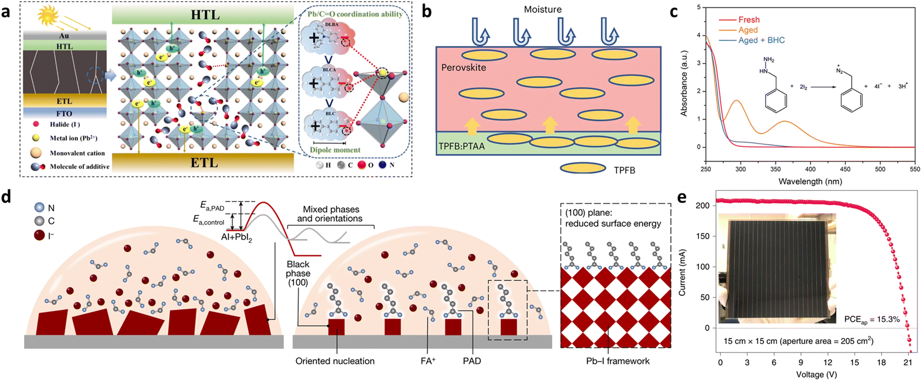 | ||
| Fig. 14 (a) Action mechanism diagram of additive dipole effect on perovskite film.194 Copyright 2023, Wiley-VCH GmbH. (b) Schematic diagram of how TPFB prevented the damage of water to perovskite. Yellow arrows indicate the spread of TPFB from the HTL to perovskite film.180 Copyright 2023, Springer Nature. (c) Ultraviolet (UV)–visible absorption spectra of the fresh and aged 1.37 M MAI:FAI (7:3) before and after adding BHC.172 (d) Schematic illustration of the thermodynamic driving force and the kinetics of the oriented nucleation of perovskite films.195 Copyright 2023, Springer Nature. (e) Cross-section SEM image of the fully blade-coated perovskite solar sub-module.196 Copyright 2022, Springer Nature. | ||
Additionally, it is worth mentioning that the addition of the salt has been demonstrated as an excellent modulation strategy. Uddin et al.197 incorporated a zinc metal salt, zinc trifluoromethane sulfonate (Zn(OOSCF3)2), which effectively suppressed iodine vacancies by utilizing the iodine reduction capability of CF3SOO−. During the crystallization process, the presence of Zn2+ ions accelerated the nucleation rate. Furthermore, a series of experiments involving the replacement of the anion verified the synergistic passivating effect of this couple of ions. This strategy successfully achieved large-area modules exceeding 100 cm2 with a certified efficiency of 19.21%. Chen et al.172 explored a cost-effective and efficient reducing additive, benzylhydrazine hydrochloride (BHC), which suppressed the molecularization tendency of iodine in the aging solution (Fig. 14c). In addition, Shi et al.195 introduced the small molecule salt pentanamidine hydrochloride (PAd) and utilized the strong interaction between amidinium and PbI2 to induce unidirectional crystal growth along (100), skipped the inferior intermediate δ-phase (Fig. 14d). As a result, a 21.4% certificated minimodule was fabricated to prove the scaling up ability. This characteristic extended the shelf life of the precursor solution and significantly reduced the time and material costs associated with large-scale production. Their efforts resulted in a blade-coated module achieving a certified efficiency of 18.2%. Methylammonium chloride (MACl) is widely used as an powerful organic halide salt additive in FA-based perovskite systems, but previous investigations have mainly focused on small-scale explorations.198–200 Bu et al.196 conducted a study on the application of MACl in large-scale films. They discovered that MACl can significantly reduce the formation energy in the FA-Cs co-A-site system, bypassing the intermediate perovskite-DMF phase and directly transforming into a dense α-phase. Through observing the annealing processes, tiny crystals gradually merged, accompanied by the volatilization of MACl, as a ripening process that resulted in the formation of complete crystals without the anti-solvent extraction. The omission of anti-solvent undoubtedly paved the way for large-scale production. Encouragingly, they achieved a blade-coated submodule with an area of 205 cm2 and a minimodule with an area of 22.4 cm2, exhibiting PCEs of 15.30% and 20.5% (Fig. 14e), respectively. Further, the addition of ionic liquids can modulate the potential aggregation problems of organic halide additives. Ding et al.20 developed an ionic liquid additive, 1,3-bis(cyanomethyl)imidazolium chloride ([Bcmim]Cl), that synergistically interacts with MACl, and regulates the aggregation of MACl. Through a series of attempts with fixed cation [Bcmim]+ and various anions, it was observed that Cl− resulted in stronger proton exchange, manifested by the increased acidity trend in the solution and broadened peaks in 1H NMR spectra. Helium ion microscopy coupled with secondary ion mass spectromet (HIM-SIMS) analysis demonstrated that the incorporation of this ionic liquid dispersed the aggregated MACl, with [Bcmim]+ being dispersed at the grain boundaries, inducing larger crystal formation and reducing defect density. Ultimately, this strategy enabled them to achieve a certified-PCE record of 23.30% for a blade-coated minimodule.
5.3 Interface modification
Interface modification regulates charge transfer and reduces energy losses in PSMs by introducing functional materials at the interfaces. These functional materials can adjust the energy level alignment, enhance light absorption, improve charge separation efficiency, and thus enhance the photovoltaic conversion efficiency and stability.95,201–203Defect trap states are highly detrimental as they significantly impact both the stability and efficiency of perovskite materials in PSMs. Currently, researchers have identified a range of interface passivation agents that can effectively mitigate the trap states on the surface. For instance, inorganic salts are being utilized to reconstruct the perovskite surface, thereby enhancing carrier mobility and reducing recombination. Additionally, organic polymer materials are being employed to crosslink and anchor free ions, minimizing ion migration and improving the interface characteristics. Rana et al.102 introduced a hydrophobic fluorinated anilinium benzylphosphonate (FABP) as a fully organic passivation agent. By utilizing ammonium and phosphonate groups, they employed a double recombination anchoring mechanism that highlighted the inherent thermal stability of the FACs organic–inorganic hybrid perovskite Cs0.15FA0.85Pb(I0.83Br0.17)3, while maintaining over 90% of the initial efficiency after 850 hours of sunlight exposure. They demonstrated the feasibility of this large-scale module fabrication process using slot-die coating and achieved an efficiency of 19.28% on an active area of 58.5 cm2 (Fig. 15a). Fei et al.95 incorporated PTAA with BCP to chelate the free Pb2+ ions at the interface of perovskite, effectively eliminating the formation of a several tens of nanometers thick amorphous layer caused by DMSO evaporation (Fig. 15b). This approach addressed the bottom surface defects that commonly occur during the top-down crystallization of FA0.9Cs0.1PbI3 perovskite films using the N2 air-knife-assisted blade coating process.204 As a result, the efficiency of the minimodule was improved to 21.8% while the small blade-coated cells’ was 24.6%. Here, our research group published a surface modifier called N,N-diphenylguanidine monohydrobromide (DPGABr), which can reconstruct the surface within a few hundred milliseconds under blade coating, achieving over 24% PCE on blade-coated small-area PSCs in the ambient air.21
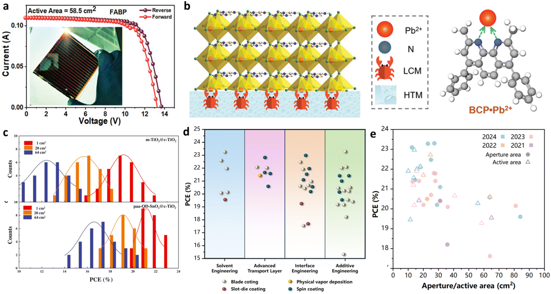 | ||
| Fig. 15 (a) J–V curve of the best-performing FABP passivated PSMs.102 Copyright 2023, Wiley-VCH GmbH. (b) Illustration of the chelation of the lead chelation molecules (LCMs) (in the HTL) with Pb2+ ions at the bottom side of the perovskite films.95 Copyright 2023, American Association for the Advancement of Science. (c) A statistical distribution of the PCE for PSCs with different ETLs.205 Copyright 2022, American Association for the Advancement of Science. (d) PCE advances in PSMs categorized by improvement strategies and deposition approaches; (e) aperture/active area and year of publication. | ||
In addition, there has been a wave of research focused on the design of novel transport layers. Instead of repairing the interfaces, the strategy of creating new interface systems with materials that exhibit higher charge carrier mobility has gained attention. The development of efficient transport layers can induce a more favorable energy level alignment, thereby reducing losses due to non-radiative recombination. Kim et al.205 designed a new ETL composed of polyacrylic acid (PAA)-stabilized tin(IV) oxide quantum dots (QD-SnO2) as an alternative to the traditional mesoporous titanium dioxide (m-TiO2) to reduce optical losses at the interface caused by reflection and interference (Fig. 15c). They achieved a minimodule PCE of 21.7% with a 20 cm2 active area. The carboxyl groups of PAA are tightly cross-linked with compact-TiO2 (c-TiO2), forming an excellent electron-selective contact and optimizing energy level alignment. External quantum efficiency (EQE) measurements confirmed that the Jsc of the FAPbI3 system was increased to over 26 mA cm−2. Moreover, the electro-luminescence EQE (EQEEL) decreased from 8.3% to 2.5%, indicating a significant reduction of non-radiative recombination by 80%. Besides, Zhou et al.158 synthesized a novel HTL material T2, which possesses a deeper highest occupied molecular orbital (HOMO). They achieved a PCE of 21.45% on a solvent-free, dual-source CVD platform with an effective area of 14.4 cm2. The introduction of thiomethyl groups with sulfur atoms in T2 allowed for the anchoring of non-coordinated Pb2+ ions at the perovskite interface. Additionally, from a band alignment perspective, T2 exhibited better system-level energy level alignment with both the perovskite and top Au electrode compared to the traditional 2,2′,7,7′-tetrakis(N,N-di-p-methoxyphenylamine)-9,9′-spirobifluorene (spiro-OMeTAD).
Moreover, SAM materials have been considered a promising and effective solution for fixing or replacing HTL by reinforcing anchoring effects. For instance, the three-tooth structure strengthened the anchoring effect of the phosphate groups in SAM directly with TCO to improve the current leakage206 and the NiOx-SAM strong linkage modification for the perovskite buried interface.207 Regarding the application of SAMs in large-scale PSMs, their utilization is still relatively uncommon. Fortunately, Ren et al.202 made preliminary explorations in this area. They polymerized a well-investigated tiny molecule SAMs, (4-(3,6-dimethyl-9H-carbazol-9-yl)butyl)phosphonic acid (Me-4PACz), into a long-chain structure. By implementing the N2 air-knife assisted blade coating process, they achieved a PCE of 20.7% on a module with an aperture area of 25 cm2 and enhanced the stability to over 1400 hours. Unlike single unit molecules, this denser polymerized structure exhibited reduced sensitivity during anchoring to the TCO, thereby widening the processing window. It resulted in a longer fluorescence lifetime of 633 ns. Additionally, the phosphonic acid groups passivated the buried interface of the perovskite, reducing non-radiative recombination and significantly improving the FF to 83.9%. By optimizing the perovskite thin film and modifying the interface, the photovoltaic efficiency of HTL-free and ETL-free PSCs has significantly surpassed 24%. Zhu et al.208 introduced the SAM into the perovskite precursor solution to deposit and bind it to ITO, ultimately achieving a high-efficiency HTL-free inverted structure device with a record PCE of 24.5% with the assistance of larger Me-4PACz molecules. Additionally, using spin-coating techniques, they achieved a high PCE of 22.5% on a 1 cm2 area. These findings collectively demonstrate the significant potential and advantages of TL-free structures. These structural optimization and innovations will further promote the development of PSCs as a renewable energy technology with promising applications.
This chapter presents a thorough examination of the crucial strategies for enhancing the performance of PSMs, which include additive engineering, solvent engineering, and interface modification. Table 3 and Fig. 15d and e have been utilized to respectively encapsulate the recent progressions in PSMs, delineating them based on effective area and chronological categorization, as well as the processing methodologies and strategic approaches employed. By analyzing these methods comprehensively, it becomes evident that their shared principles and mechanisms primarily manifest in three key areas. Initially, optimizing crystal quality and managing defects is vital. The selection of additives and solvents can notably improve the nucleation and growth processes of perovskite crystals. For instance, by controlling solvent evaporation rates or introducing Lewis basic additives, it is possible to enhance grain size and reduce defect density, thereby boosting photovoltaic performance.20,189–192,197 Furthermore, interface modification strategies enhance carrier dynamics by improving energy level alignment. The utilization of organic polymers or inorganic salts as passivation agents not only enhances interface charge transfer but also improves the long-term stability of devices. Lastly, auxiliary optimization strategies for large-scale processing are essential for industrial production. Achieving uniformity and stability necessitates addressing challenges such as optimizing solvent systems, incorporating interface materials suitable for high-throughput preparation, and developing adjustable film-forming processes. Future research should explore the synergistic effects of these strategies, emphasizing scalability and cost-effectiveness.158,205 Additionally, it is crucial to adopt environmentally friendly practices to mitigate recycling challenges. For example, the utilization of green solvents like ACN is pivotal for advancing the commercial development of perovskite solar technology.188,195
| Perovskite composition | Type | Effective materials | Perovskite process type | Assist mode | PCE (%) | Aperture/active areaa (cm2) | Year | Ref. |
|---|---|---|---|---|---|---|---|---|
| CThe PCE has been certified by a recognised authority. 1Aperture area. 2Active area. a Since authors use different statistical scales for area, in order to avoid ambiguity, we use superscripts 1 and 2 to represent aperture area and active area (without considering GFF) respectively for ease of understanding. | ||||||||
| Cs0.05MA0.05FA0.9Pb(I1−xClx) | Additive engineering | [Bcmim]Cl | Blade coating | N2 air knife | 23.3C | 27.221 | 2024 | 20 |
| Cs0.1FA0.9PbI3 | Solvent engineering | NEP | Blade coating | Vacuum | 23.28C | 22.961 | 2024 | 118 |
| 22.55C | 57.131 | |||||||
| FAPbI3 | Solvent engineering | DMF | Blade coating | N2 air knife | 23.09C | 12.41 | 2024 | 164 |
| ((FA0.95Cs0.05)PbI3)0.975(MAPbBr3)0.025 | Interface treatment | SnO2 with different oxygen vacancies level | Spin coating | Anti-solvent | 22.96 | 142 | 2024 | 163 |
| Rb0.03Cs0.05MA0.05FA0.90PbI3 | Advanced ETL Materials | TiO2 nanoparticles | Spin coating | Vacuum | 22.72C | 24.632 | 2022 | 209 |
| FAPbI3 | Interface treatment | Trifluoroacetate (TFA−) and 3,3-diphenylpropylammonium (DPA+) | Blade coating | N2 air knife | 22.47 (20.50C) | 251 | 2024 | 210 |
| 20.88 | 641 | |||||||
| FA0.9Cs0.1PbI3 | Additive engineering | Ferrocenium hexafluorophosphate (FcPF6) | Blade coating | Vacuum | 22.13 | 361 (182) | 2024 | 211 |
| 20.27 | 1001 (562) | |||||||
| FA0.9Cs0.1PbI3 | Advanced HTL Materials | [2-(9-Ethyl-9H-carbazol-3-yl)ethyl]phosphonic acid (EtCz3EPA) | Blade coating | Regular annealing | 22.1 | 17.881 | 2024 | 179 |
| MA0.7FA0.3PbI3 | Advanced HTL Materials | Poly-DBPP | Blade coating | N2 air knife | 22 | 30.031 | 2024 | 173 |
| FAPbI3 | Additive engineering | Perfluoroalkylsulfonyl quaternary ammonium iodide (FSAI) | Blade coating | N2 air knife | 22 | 15.642 | 2024 | 212 |
| FA0.92MA0.08PbI2.76Br0.24 | Interface treatment | 2-Chloro-5-(trifluoromethyl)-phenylammonium bromide | Spin coating | Regular annealing | 21.9 | 102 | 2024 | 165 |
| FAPbI3 | Solvent engineering | ACN | Blade coating | N2 air knife | 21.9 | 15.642 | 2023 | 193 |
| FA0.9Cs0.1PbI3 | Interface treatment | BCP | Blade coating | Regular annealing | 21.8C | 26.91 | 2023 | 95 |
| Cs0.05MA0.05FA0.9PbI3 | Advanced HTL Materials | A novel spiro-type HTM ‘DP’ | Spin coating | vacuum | 21.78C | 27.861 | 2023 | 213 |
| FAPbI3 | Advanced HTL Materials | Polyacrylic acid-stabilized tin(IV) oxide quantum dots | Spin coating | Anti-solvent | 21.7C | 202 | 2022 | 205 |
| 20.6C | 642 | |||||||
| Cs0.05MA0.1FA0.85PbI2.9Br0.1 | Interface treatment | Phenethylammonium bromide (PEABr) and polymethyl methacrylate (PMMA) | Spin coating | Anti-solvent | 21.56 | 13.682 | 2024 | 214 |
| FAPbI3 | Advanced HTL Materials | A novel spiro-type HTM 'T2' | PVD | None | 21.45 | 14.41 | 2024 | 158 |
| FAPbI3 | Additive engineering | PAd | Spin coating | Vacuum | 21.4C | 27.831 | 2023 | 195 |
| Cs0.05FA0.85MA0.10Pb(I0.97Br0.03)3 | Additive engineering | Fullerene derivative 4-(1′,5′-dihydro-1′-methyl-2′H-[5,6] fullereno-C60-Ih-[1,9-c]pyrrol-2′-yl) phenylphosphonic acid (CPPA) | Spin coating | Vacuum | 21.4 (19.6C) | 17.11 | 2023 | 215 |
| Cs0.05(FA0.9MA0.1)0.95Pb(I0.9Br0.1)3 | Module protection | O3 | Spin coating | Anti-solvent | 21.37C | 12.841 | 2023 | 61 |
| FAPbI3 | Interface treatment | Benzamidine hydrochloride (PFACl) | Spin coating | Regular annealing | 21.2 | 13.442 | 2023 | 216 |
| FAPbI3 | Additive engineering | Thermotropic liquid crystals 3,4,5-trifluoro-4′-(trans-4-propylcyclohexyl)biphenyl (TFPCBP) | Spin coating | Vacuum | 21.1C | 311 | 2024 | 217 |
| MA0.7FA0.3PbI3 | Interface treatment | Me-4PACz | Blade coating | N2 air knife | 20.7 | 251 | 2023 | 202 |
| FAPbI3 | Interface treatment | Carbon disulfide (CS2) vapour | Blade coating | Undisclosed | 20.66 | 40.62 | 2023 | 218 |
| Cs0.05FA0.95PbI3 | Interface treatment | Dimethylammonium trifluoroacetate (DMATFA) | Spin coating | Vacuum | 20.58 | 63.741 | 2024 | 219 |
| FA0.88Cs0.12PbI3 | Additive engineering | MACl | Blade coating | Air knife | 20.5 | 22.41 | 2022 | 196 |
| 15.3 | 2051 | |||||||
| FA0.83Cs0.17PbI3 | Solvent engineering | NMP | Slot-die coating | Air knife | 20.42 (19.3C) | 17.12 | 2021 | 220 |
| 19.54 | 652 | |||||||
| FA0.95MA0.05PbI2.85Br0.15 | Additive engineering | 1-Butyl-3-methylimidazolium thiocyanate (BMIMSCN) | Blade coating | Regular annealing | 20.4 | 102 | 2022 | 221 |
| (FAPbI3)0.95(MAPbBr3)0.05 | Interface treatment | Acetylcholine bromide (ACBr) | Blade coating | N2 air knife | 20.4 (17.53C) | 311 | 2021 | 222 |
| MA0.7FA0.3PbI3 | Additive engineering | TPFB | Blade coating | N2 air knife | 20.2 (19.2C) | 221 | 2023 | 180 |
| Cs0.05MA0.05FA0.9PbI3 | Interface treatment | Potassium borohydride (KBH4) | Spin coating | Vacuum | 20.2 | 291 | 2024 | 223 |
| FA0.90MA0.03Cs0.07Pb(I0.92Br0.08)3 | Additive engineering | DLBA | Spin coating | Anti-solvent | 20.18 | 142 | 2023 | 194 |
| (FAPbI3)0.95(MAPbBr3)0.05 | Solvent engineering | DMI | Blade coating | Air knife | 20.10 | 361 | 2023 | 191 |
| 20.15 | 811 | |||||||
| MA0.7FA0.3PbI3 | Additive engineering | Zn(OOSCF3)2 | Blade coating | N2 air knife | 19.60C | 841 | 2024 | 197 |
| 19.21C | 1081 | |||||||
| FA1−xMAxPb(I1−yBry)3 | Additive engineering | 2-(N-Morpholino)ethanesulfonic acid potassium salt (MESK) | Blade coating | N2 air knife | 19.45 | 11.352 | 2024 | 181 |
| Cs0.15FA0.85Pb(I0.83Br0.17)3 | Interface treatment | FABP | Slot-die coating | N2 air knife | 19.28 | 58.52 | 2023 | 102 |
| 17.62 | 641 | |||||||
| MA0.7FA0.3PbI3 | Additive engineering | BHC | Blade coating | N2 air knife | 18.2 | 35.81 | 2021 | 172 |
6. Device encapsulation and stability tests
Researchers have made significant breakthroughs in the PCE of PSMs as they gradually acquire the fabrication processes of the functional layers on a larger scale.20,158,209,224 However, to achieve commercialization and large-scale production, enhancing the stability of PSMs is a topic that deserves deep consideration. The instability issues of PSMs can be divided into two fields, intrinsic and extrinsic. Intrinsic factors include the instability caused by phase transitions and defects in perovskite materials, while extrinsic factors involve rapid aging and degradation induced by environment heat, moisture, and oxygen.225–228The internal instability of perovskite materials is closely intertwined with their structural and chemical stability. The mathematical formulation of the Goldschmidt tolerance factor t229 can be expressed as follow:
 | (20) |
 | ||
| Fig. 16 (a) Tolerance factors distribution of different perovskite compositions.233 Copyright 2022, Wiley-VCH GmbH (b) The instability stress sources of perovskite materials.234 | ||
Additionally, UV radiation is a critical factor that triggers photodegradation, charge defects, and lattice distortions in perovskite materials. Elevated temperatures accelerate lattice expansion and ion migration processes, contributing to decreased material stability. Mechanical stress, such as bending and stretching, can cause cracks and fractures in the perovskite layer, consequently reducing module performance and lifespan. Furthermore, light intensity and spectral composition influence the stability of perovskite materials, with high-intensity light and specific wavelengths leading to material degradation and deterioration.235 Take MAPbI3 as an example, the pathway of perovskite degradation is illustrated in Fig. 16b.234 Simultaneously, during the real-life operation of PSMs, it has been found that the stability of PSMs is also affected by factors such as layer delamination and potential-induced degradation (PID). The multi-layer structure of PSMs inherently introduces challenges related to delamination, primarily stemming from the lamination process and differential thermal expansion characteristics across layers. Delamination issues manifest in two key areas: the separation between encapsulation materials and the device, and internal delamination within the device itself. The former is chiefly influenced by the properties of the encapsulation materials, with considerations such as water vapor and air barrier capabilities, as well as mechanical resistance playing pivotal roles. Multi-layer encapsulation236,237 and advanced lamination processes238,239 can effectively improve the resistance to delamination. In rare cases, delamination will occur immediately after an immature lamination process.240 However, the delamination phenomenon between layers inside PSMs is different. Erdil et al.240 tested the relationship between each layer through indoor thermal cycle testing and found that this phenomenon is dominated by temperature fluctuations. The ETL part of C60 and SnO2 is the most likely to fall off in the entire structure. We were surprised to find that this coincides with the delamination phenomenon of SnO2 often encountered in vacuum annealing in Qi et al.'s48 exploration of CVD preparation of PSMs in Section 3.4.1. These findings have promoted in-depth research on advanced thermally stable carrier transport materials and thermal insulation packaging materials. Additionally, PID is manifested as a significant decline in the performance of photovoltaic devices under the influence of an external voltage bias or internal electric field, which is caused by the high voltage difference between the module and the ground during operation.241 In traditional silicon solar modules (SSMs), PID is observed as the migration of alkali metal ions, such as sodium ions (Na+), in soda lime glass when the device is at a negative potential to the ground, which can cause rapid and catastrophic damage.242–244 In addition to the impacts similar to those in SSMs, which mainly come from the packaging materials, perovskite has unique ionic properties and the multiple impacts of PID caused by its internal high ion migration activity are more serious and fatal to stability.245,246 Interestingly, Zhang et al.241 found that after applying −1500 V negative bias for 18 hours, the diode characteristics of the device gradually disappeared and could be quickly recovered to 80% in dark storage. They believed that this recoverability was due to the ion migration performance of perovskite, which enabled the Na+ driven by the bias to migrate quickly out of the perovskite layer. Researchers are still exploring the mechanisms involved, but some strategies have been found to alleviate PID to a certain extent by selecting proper functional layer and interlayer buffer strategies. Zeel et al.246 found that using PC61BM as ETL in n–i–p can temporarily reduce PID, with only 4% performance loss under 18 hours of continuous bias. NiOx barrier layer was found by Nakka and colleagues247 that successfully kept Na+ away from perovskite and reduced the PCE loss from 73% to 35%. Currently, the IEC 62804-1-1 technical specification defines the test method for crystalline silicon PV modules,248 but there is no specific PID test standard for PSMs. Research papers generally utilize the horizontal comparison of performance degradation under the condition of applying a negative bias of −1000 V. Given this, we contend that with the deepening industrial deployment, it is imperative to establish more standardized and comprehensive industry testing standards to evaluate the stability factors of both internal and external placements and operations at various stages. This initiative aims to bolster the commercial impetus of PSMs and enhance customer assessment criteria.
6.1 Device encapsulation
Encapsulation, which is considered by an increasing number of scientists to be a consensus in development, serves as a direct and effective bidirectional protective measure. It effectively isolates the extrinsic complex environment that accelerates aging while also preventing the leakage of lead in PSMs from impacting the extrinsic environment.249 Due to the unique degradation mechanisms and fragile stability of PSMs, the primary task is to ensure isolation from water and oxygen. For PSMs, although we all know that encapsulation technology is a commercially indispensable technological barrier, the exploration of encapsulating technology is still far behind the focus on performance at the current stage. The main parameters affecting the encapsulation of the material are shown in Table 4.226| Characteristics | Specification or requirement |
|---|---|
| WVTR | 10−4–10−6 g m−2 day−1 |
| OTR | 10−3–10−5 cm3 m−2 day−1 atm−1 |
| T g | <−40 °C (during winter in deserts) |
| Total hemispherical light transmission over the wavelength range from 400 nm to 1100 nm | >90% of incident light |
| Hydrolysis | None (80 °C, 100% RH) |
| Water absorption | <0.5 wt% (20 °C/100% RH) |
| Resistance to thermal oxidation | Stable (up to 85 °C) |
| Mechanical creep | None (90 °C) |
| Tensile modulus | <20.7 MPa (<3000 psi) at 25 °C |
| Chemical inertness | No reaction (with embedded Cu coupons at 90 °C) |
| UV absorption degradation | None (>350 nm) |
| Hazing or clouding | None (80 °C, 100% RH) |
Due to the light absorption window being restricted to the bottom surface, the optimal encapsulating technique for PSMs corresponds to that of SSMs, employing a single-sided glass vacuum lamination process. This process can be categorized into two distinct pathways, the thin-film encapsulation (TFE) from the top to the bottom, and the edge seal (ES) from the side to the center, as depicted in Fig. 17a.250 Both these two processes offer excellent encapsulating performance. ES is considered a more cost-effective encapsulating solution as it requires less material. However, in the field of flexible encapsulating, TFE surpasses ES since the encapsulation material has a smaller contact area and mechanical side stress in ES, leading to potential seal damage during bending. At present, commercial polymer demonstrate excellent performance in both TFE and ES processes and can be uniformly applied to the device using spin coating or injection methods. Traditional polymers such as PMMA,251–253 ethyl vinyl acetate (EVA),254 and polycarbonate (PC),227etc. have shown promising results in TFE. With the increasing area of functional layer deposition, the TFE encapsulation mode also requires materials with corresponding extensibility to serve PSMs and better facilitate commercial applications. PMMA, known for its high impact resistance and thermal stability, is widely utilized in the circuit printing field. Typically prepared via spin coating, PMMA usage aligns with the challenges faced in the laboratory-scale expansion of PSCs. Hughes et al.255 addressed this issue by adjusting the solvent environment of PMMA, designing uniformly dispersed encapsulants in ethyl acetate. This innovative approach provided a PSM-friendly solution idea for large-area coating using a spray coating process. Moreover, PC is considered to be a good packaging material due to its excellent flexibility, but its high roughness is seldom used in large area packaging. Skafi et al.256 used a blade coating method to reduce its roughness from over 1400 nm to 23 nm by applying a resin mixture and enhanced its chemical resistance, which provides an imaginative way for PC to be used in large area PSMs.
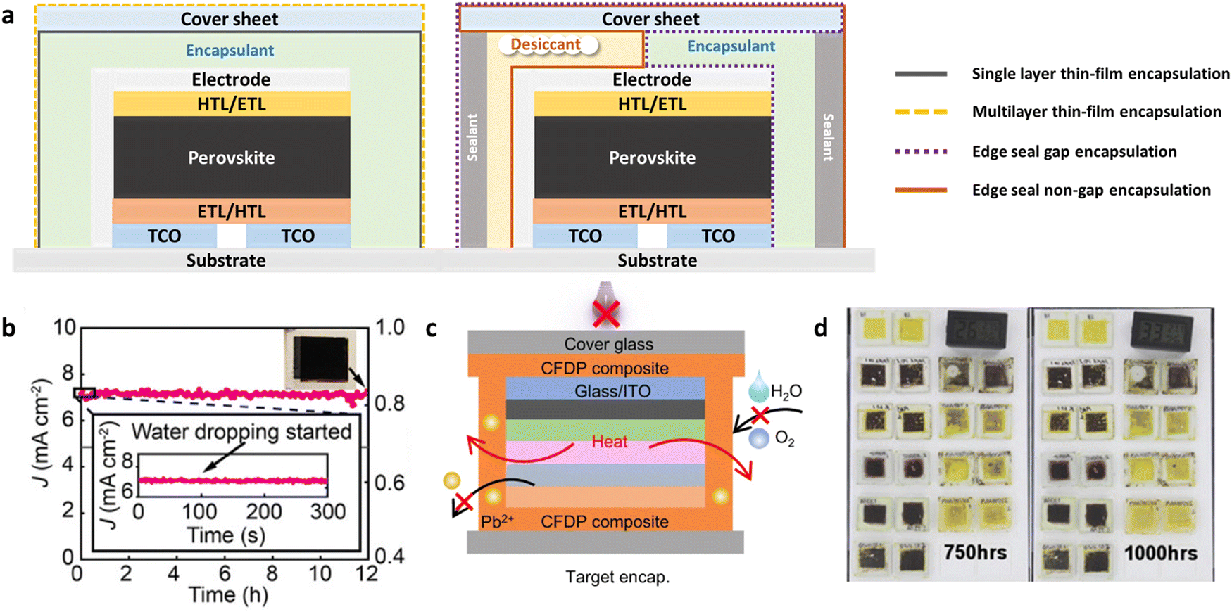 | ||
| Fig. 17 (a) Schematic diagrams of different TFE and ES encapsulation approaches. (b) High stability performance under water drop stress.136 (c) Schematic of CFDP package without UV irradiation.257 (d) The degradation performance after 750 and 1000 hours.258 Copyright 2016, Elsevier Ltd. | ||
Furthermore, more recent research on advanced encapsulation materials has also seen new developments, which especially affect several narrow protective capabilities. In addition to glass encapsulation, Mai et al.136 explored novel encapsulation techniques by introducing Glaco, a commercialized thin nanostructured super-repellent coating material. They successfully induced an advancing contact angle greater than 167° and a contact angle hysteresis less than 10°. This method significantly enhanced the waterproofing performance of the devices from nearly zero to over 12 hours of water tolerance (Fig. 17b). This provides a promising avenue for enhancing the stability against water-induced degradation. Based on existing materials and processes, the isolation of water and oxygen has generally met the requirements. However, there has been limited attention given to external thermal management and the environmental pollution caused by lead leakage. Thermal energy produced can lead to rapid ion migration, resulting in the severe degradation of perovskite materials. While Pb, as a highly toxic element, poses a significant threat to human and environmental safety if it leaks. Tong and colleagues257 developed a self-crosslinked fluoropropyl methylsiloxane-dimethylsiloxane multiblock polymer (CFDP) encapsulation material that can be processed at room temperature, eliminating the thermal instability caused by high-temperature lamination (Fig. 17c). The material maintained 95% efficiency after undergoing 220 thermal cycles. Moreover, the incorporation of carbonyl groups facilitated coordination and anchored Pb, leading to 99% leaking inhibition during a rainwater exposure test. Moreover, Qi et al.259 discovered that materials with high self-healing properties at temperatures above Tg can significantly reduce the risk of Pb leakage. They made remarkable achievements by adopting ternary additive engineering to a thermocrosslinking epoxy resin, changing Tg to 42 °C. This modification led to a staggering reduction of 375 times in lead leakage under extreme and harsh hail simulation conditions. Additionally, Mariani et al.260 discovered a new packaging material, viscoelastic (semi-solid)/highly viscous (liquid) polyolefin, which can be operated in industrial high-throughput solventless lamination. The addition of two-dimensional hexagonal boron nitride (h-BN) in the solution further enhances its adhesive, barrier, and thermal management properties. High stability was demonstrated through multiple cycles of aging tests involving light, heat, and impact.
6.2 Standardized stability tests
The encapsulated perovskite module needs to undergo a series of stability tests to evaluate its performance under different environmental conditions. However, most research papers on stability mainly focus on inconsistent simple tests like environmental storage or light soaking at present, which do not meet the stringent stability requirements for commercial products under specific conditions, limiting the full potential of the technology. Therefore, the development of guiding standards for stability testing of PSMs is pressing and imperative.Regarding traditional ground-mounted photovoltaics, which mainly refers to silicon solar arrays, the International Electrotechnical Commission (IEC) has provided a set of on-site performance testing standards known as IEC 61215.248,261 However, due to the differences in physical systems, these standards are not applicable to the new generation thin-film cells such as OPV and PSMs. In the battle to establish standards, many scholars have proposed solutions, but the problem is the inability to form unified standardized criteria. This undoubtedly hinders the transition of experimental products to the industrial production process.262–264 Therefore, in 2011, Reese et al.265 integrated and organized the major research advancements in the field and introduced the International Summit on Organic PV Stability (ISOS) protocols as a standardized aging experiment guideline. This document is not a definitive verdict but rather a standardized guidance to assist in conducting experiments in disparate research environments. It serves as a starting point and will be gradually improved as research progresses.266
The ISOS testing protocol is primarily defined by the combination of four stressors, namely, light exposure (one standard solar simulator or complete darkness), ambient contaminants (inert gases, atmospheric air, or controlled relative humidity), temperature (ambient temperature, 65 °C, or 85 °C), and electrical bias (open circuit (OC), maximum power point tracking, or +/− fixed voltage).265 Based on the different combinations of these environmental stressors, the testing protocol is divided into five stress testing tracks. ISOS-D and ISOS-L represent a complementary set of light environment stress controls. ISOS-D involves testing the device's resilience to atmospheric contents and monitoring the degradation and the formation of defects in a darkened setting. Conversely, ISOS-L entails prolonged continuous light soaking, which expedites defect formation and phase separation processes. In addition to these steady-state tests under fixed conditions, ISOS-T and ISOS-LT explore cyclic conditions. Their objective is to investigate the lifespan under the cyclic interplay of heat and light-moisture-heat, which more faithfully simulate the dynamic environmental variations of light and temperature in real-world climates. The repetitive migration of charge carriers during this process is regarded as a significant acceleration factor for aging. Recognizing that indoor testing alone cannot adequately reflect real-world scenarios like building-integrated photovoltaics, such as BIPV, ISOS-O is specifically devised for outdoor testing. It primarily focuses on statistically assessing the lifetime performance under actual outdoor conditions. Given the diverse climatic conditions across different regions, this testing approach places greater emphasis on comprehensive data collection to provide a wide range of acceleration factor information.
The new edition of ISOS offers three targeted testing protocols for PSCs to address their dual degradation mechanisms of intrinsic and extrinsic stability. The light soaking and dark mode alternating cycle testing, ISOS-LC, has been included as a supplement to assess the reversible chemical processes of metastable perovskite under light-induced degradation and recovery. In addition, studies have shown that the shielded part of the PSMs during operation will not generate current but will form a reverse bias, which will cause internal ion migration and charge carrier accumulation, forming a thermal trap. ISOS-V recommends applying bias at the MPP or OC position in the dark to enhance understanding of PSM degradation under bias. Moreover, due to the potential masking effect of sensitive gas atmospheres on the intrinsic stability performance of PSMs, the ISOS-I protocol has been included in the assessment framework. It proposes maintaining a fixed atmospheric environment to eliminate this potential drawback. This is not established as an independent measure but rather serves as an addition to the aforementioned protocols. If an inert gas environment is adopted, it is considered to comply with the ISOS-I protocol.
Furthermore, within each pathway, there are three subdivisions, allowing for fine-grained control of the testing conditions. These are designed for various experimental conditions, with Level 3 representing more stringent testing requirements and higher equipment demands in the laboratory. Level 1, on the other hand, utilizes commonly available equipment and is considered the minimum requirement for stability testing. The specific testing conditions can be found in Table 5.265,266
| Test ID | Light source (stability) | Temperature | RH | Environment/set-up | Light source (IV) | Load |
|---|---|---|---|---|---|---|
| Dark storage (ISOS-D) | ||||||
| ISOS-D-1 | None | Ambient (23 ± 4 °C) | Ambient | Ambient air | Solar simulator/sunlight | OC |
| ISOS-D-2 | None | 65, 85 °C | Ambient | Oven, ambient air | Solar simulator | OC |
| ISOS-D-3 | None | 65, 85 °C | 85% | Env. chamber | Solar simulator | OC |
| Bias stability (ISOS-V) | ||||||
| ISOS-V-1 | None | Ambient (23 ± 4 °C) | Ambient | Ambient air | Solar simulator | Positive: VMPP; Voc; Eg/q; Jsc Negative: Voc, JMPPa |
| ISOS-V-2 | None | 65, 85 °C | Ambient | Oven, ambient air | Solar simulator | |
| ISOS-V-3 | None | 65, 85 °C | 85% | Env. chamber | Solar simulator | |
| Light-soaking (ISOS-L) | ||||||
| ISOS-L-1 | Solar simulator | Ambient (23 ± 4 °C) | Ambient | Light only | Solar simulator | MPP or OC |
| ISOS-L-2 | Solar simulator | 65, 85 °C | Ambient | Light/temperature | Solar simulator | MPP or OC |
| ISOS-L-3 | Solar simulator | 65, 85 °C | ∼50% | Light/temperature/RH | Solar simulator | MPP |
| Outdoor stability (ISOS-O) | ||||||
| ISOS-O-1 | Sunlight | Ambient | Ambient | Outdoor | Solar simulator | MPP or OC |
| ISOS-O-2 | Sunlight | Ambient | Ambient | Outdoor | Sunlight | MPP or OC |
| ISOS-O-3 | Sunlight | Ambient | Ambient | Outdoor | Sunlight/solar simulator | MPP |
| Thermal cycling (ISOS-T) | ||||||
| ISOS-T-1 | None | RT to 65, 85 °C | Ambient | Hot plate/oven | Solar simulator | OC |
| ISOS-T-2 | None | RT to 65, 85 °C | Ambient | Oven/Env. chamber | Solar simulator | OC |
| ISOS-T-3 | None | −40 to +85 °C | <55% | Env. chamber | Solar simulator | OC |
| Light cycling (ISOS-LC) | ||||||
| ISOS-LC-1 | Solar simulator/Dark cycle period: 2, 8, or 24 h; Duty cycle: 1:1 or 1:2 |
Ambient (23 ± 4 °C) | Ambient | Light only | Solar simulator | MPP or OC |
| ISOS-LC-2 | 65, 85 °C | Ambient | Light/temperature | Solar simulator | MPP or OC | |
| ISOS-LC-3 | 65, 85 °C | <50% | Light/temperature/RH | Solar simulator | MPP | |
| Solar-thermal cycling (ISOS-LT) | ||||||
| ISOS-LT-1 | Solar simulator | Linear/step ramping between RT and 65 °C | Monitored, uncontrolled | Weathering chamber | Solar simulator | MPP or OC |
| ISOS-LT-2 | Solar simulator | Linear ramping between 5 °C and 65 °C | Monitored, controlled at 50% beyond 40 °C | Env. chamber with a sun simulator | Solar simulator | MPP or OC |
| ISOS-LT-3 | Solar simulator | Linear ramping between −25 °C and 65 °C | Monitored, controlled at 50% beyond 40 °C | Env. chamber with sun simulator and freezing | Solar simulator | MPP or OC |
7. Conclusions and outlook
In summary, important issues for PSMs, including structural design, scalable deposition theoretical models and methods, fabrication technologies for high-quality functional layers, and product-oriented encapsulation and stability testing have been systematically investigated in recent years. Encouragingly, through collaborative efforts in both the academic and industrial communities, minimodules and large modules exceeding 800 cm2 have achieved PCE of over 23% and 20%,20,37 respectively, gradually approaching the energy conversion performance of silicon solar modules. However, considering commercialization demands, efficiency, stability, and safety are all essential and require further enhancement. In producing large PSMs, three critical steps: functional layer deposition, scribing, and encapsulation, will play decisive roles in addressing these urgent needs.Several advancements can be observed from a materials-to-devices perspective on the manufacturing steps of PSMs. Firstly, interface, solvent, and additive engineering have been identified as effective means to adjust the inherent crystal structure and morphology, thereby enhancing efficiency and intrinsic stability in materials and physical theory. Device performance can be significantly improved by integrating chemical mechanisms such as anchoring and intermediates, along with energy level alignment between functional layers. Recent developments in surface passivation molecules provide researchers with improved methods for modifying shallow surface morphology. Secondly, the exploration of high-throughput and uniform deposition processes has facilitated the rapid industrialization and scale-up of PSMs. In particular, the mainstream meniscus coating technology warrants further investigation into the harmonious relationship between coating machine process parameters and the fluid dynamics of precursor solutions. Currently, the highest efficiencies in this process have been achieved through air knife-assisted fluid dynamics engineering for interface morphology control, indicating substantial potential for further development. In contrast, meniscus coating and printing technologies present more promising avenues for scalability. Thirdly, the limits of active area utilization are being continuously pushed by enhancing laser precision and patterning. Although breakthroughs such as the low dead zone technology achieving over 99.5% GFF for minimodules have been reported, the application area remains less than 3 cm2 and further exploration into reliability and reproducibility in larger-area devices is warranted.60 Fourthly, in terms of product durability and stability, perovskite materials are still highly sensitive. During large-area deposition, mixed components such as MAxFA(1−x)PbI3 and FAxCs(1−x)PbI3 have demonstrated superior chemical and operational stability within existing technologies, which merits attention. When addressing long-term operational concerns, encapsulation serves as a robust protective measure that can significantly mitigate the bidirectional penetration impacts on PSMs, including external mechanical and environmental influences, as well as internal material degradation and toxic material leakage. The single-sided glass vacuum lamination process is regarded as a suitable approach for application in PSMs due to its rapid and straightforward production workflow. Fifthly, the ISOS standards for perovskite stability testing represent an essential framework for the commercialization of PSMs, providing impetus for the emergence of better products. However current literature predominantly focuses on stability testing related to light soaking and cycling, while further exploration of thermal cycling and ultraviolet stability testing remains necessary.
On the basis of the increasingly mature technology in a single junction, tandem PSMs with a high theoretical efficiency limit have attracted wide attention. Among various technological pathways, silicon/perovskite tandems have demonstrated the most outstanding performance levels, reaching 34.6%.13 The control of interface states between materials poses a significant challenge as the number of layers increases. Simultaneously, with an increasing number of interfaces, the phenomenon of delamination during long-term device operation will become more complex. Furthermore, by exploiting the tunable bandgap properties of perovskite, precise design of photoelectric matching for wide and narrow bandgap subcells is necessary to avoid spectral overlap and energy wastage.267–269 With the current emergence of industrialization, the development of portable PSMs with functionalities such as flexibility and semi-transparency is a promising direction to meet diverse commercial demands. This opens up rich possibilities for wearable electronic applications. The bending resistance of F-PSMs is critically important, posing new challenges for the stability of their transport layers, perovskite materials, and the secure contact at interfaces. Moreover, their compatibility with R2R production methods makes it essential to explore large-scale printing processes that facilitate collaborative interactions among various material systems. Semi-transparent PSMs can be applied in contexts such as solar windows, significantly enhancing solar energy utilization, particularly in urban environments. Additionally, the inevitable leakage of lead from high-performance PSMs poses negative risks to both human health and the environment. The fatigue of materials in F-PSMs can further accelerate this leakage, making the exploration of lead-free perovskite components a crucial research avenue. Furthermore, it is necessary to develop specialized encapsulation materials and process to address these concerns effectively for unavailability due to rigid cover sheet.
Data availability
Data availability is not applicable to this article as no new data were created or analyzed in this study.Conflicts of interest
The authors declare no conflict of interest.Acknowledgements
This work is financially supported by the Research Center for Organic Electronics of the Hong Kong Polytechnic University (Project No. 1-CE0P). This work is also supported by the Research Grants Council of Hong Kong, China (Project No. 15306822) and the project of strategic importance of the Hong Kong Polytechnic University (Project No. ZE2X).References
- H. H. Liu, A. G. Aberle, T. Buonassisi and I. M. Peters, Sol. Energy, 2016, 135, 598–604 Search PubMed.
- F. Li, F. R. Lin and A. K. Jen, Adv. Mater., 2024, 36, 2307161 CAS.
- Global Market Outlook For Solar Power 2023 - 2027, https://www.solarpowereurope.org/insights/market-outlooks/global-market-outlook-for-solar-power-2023-2027-1, (accessed 11, 2023) Search PubMed.
- Solar Panels Market Outlook & Forecasts 2024-2029: Green Building Initiatives Drive Demand, Enhancing Energy Efficiency and Sustainability, https://www.businesswire.com/news/home/20240902284683/en/Solar-Panels-Market-Outlook-Forecasts-2024-2029-Green-Building-Initiatives-Drive-Demand-Enhancing-Energy-Efficiency-and-Sustainability---ResearchAndMarkets.com Search PubMed.
- D.-Y. Son, J.-W. Lee, Y. J. Choi, I.-H. Jang, S. Lee, P. J. Yoo, H. Shin, N. Ahn, M. Choi, D. Kim and N.-G. Park, Nat. Energy, 2016, 1, 16081 CrossRef CAS.
- J. S. Manser and P. V. Kamat, Nat. Photonics, 2014, 8, 737–743 CrossRef CAS.
- S. De Wolf, J. Holovsky, S.-J. Moon, P. Loper, B. Niesen, M. Ledinsky, F.-J. Haug, J.-H. Yum and C. Ballif, J. Phys. Chem. Lett., 2014, 5, 1035–1039 CrossRef CAS.
- T. Miyasaka, Chem. Lett., 2015, 44, 720–729 CrossRef CAS.
- V. Gonzalez-Pedro, E. J. Juarez-Perez, W.-S. Arsyad, E. M. Barea, F. Fabregat-Santiago, I. Mora-Sero and J. Bisquert, Nano Lett., 2014, 14, 888–893 CrossRef CAS PubMed.
- J. Burschka, N. Pellet, S.-J. Moon, R. Humphry-Baker, P. Gao, M. K. Nazeeruddin and M. Grätzel, Nature, 2013, 499, 316–319 CrossRef CAS PubMed.
- J. M. Frost, K. T. Butler, F. Brivio, C. H. Hendon, M. van Schilfgaarde and A. Walsh, Nano Lett., 2014, 14, 2584–2590 CrossRef CAS.
- A. Kojima, K. Teshima, Y. Shirai and T. Miyasaka, J. Am. Chem. Soc., 2009, 131, 6050–6051 CrossRef CAS PubMed.
- Interactive Best Research-Cell Efficiency Chart, https://www.nrel.gov/pv/interactive-cell-efficiency.html Search PubMed.
- M. Yang, D. H. Kim, T. R. Klein, Z. Li, M. O. Reese, B. J. Tremolet de Villers, J. J. Berry, M. F. A. M. van Hest and K. Zhu, ACS Energy Lett., 2018, 3, 322–328 CrossRef CAS.
- K. Xiao, R. Lin, Q. Han, Y. Hou, Z. Qin, H. T. Nguyen, J. Wen, M. Wei, V. Yeddu, M. I. Saidaminov, Y. Gao, X. Luo, Y. Wang, H. Gao, C. Zhang, J. Xu, J. Zhu, E. H. Sargent and H. Tan, Nat. Energy, 2020, 5, 870–880 CrossRef CAS.
- J. Zhuang, P. Mao, Y. Luan, N. Chen, X. Cao, G. Niu, F. Jia, F. Wang, S. Cao and J. Wang, Adv. Funct. Mater., 2021, 31, 2010385 Search PubMed.
- L. A. Castriotta, M. Zendehdel, N. Yaghoobi Nia, E. Leonardi, M. Löffler, B. Paci, A. Generosi, B. Rellinghaus and A. Di Carlo, Adv. Energy Mater., 2022, 12, 2103420 CrossRef CAS.
- Y. Xiao, C. Zuo, J.-X. Zhong, W.-Q. Wu, L. Shen and L. Ding, Adv. Energy Mater., 2021, 11, 2100378 CrossRef CAS.
- F. Matteocci, S. Razza, F. Di Giacomo, S. Casaluci, G. Mincuzzi, T. M. Brown, A. D'Epifanio, S. Licoccia and A. Di Carlo, Phys. Chem. Chem. Phys., 2014, 16, 3918–3923 CAS.
- B. Ding, Y. Ding, J. Peng, J. Romano-deGea, L. E. K. Frederiksen, H. Kanda, O. A. Syzgantseva, M. A. Syzgantseva, J.-N. Audinot, J. Bour, S. Zhang, T. Wirtz, Z. Fei, P. Dörflinger, N. Shibayama, Y. Niu, S. Hu, S. Zhang, F. F. Tirani, Y. Liu, G.-J. Yang, K. Brooks, L. Hu, S. Kinge, V. Dyakonov, X. Zhang, S. Dai, P. J. Dyson and M. K. Nazeeruddin, Nature, 2024, 628, 299–305 CAS.
- J. Zhuang, C. Liu, B. Kang, H. Cheng, M. Xiao, L. Li and F. Yan, Adv. Mater., 2023, 2309869 Search PubMed.
- P. J. S. Rana, B. Febriansyah, T. M. Koh, B. T. Muhammad, T. Salim, T. J. N. Hooper, A. Kanwat, B. Ghosh, P. Kajal, J. H. Lew, Y. C. Aw, N. Yantara, A. Bruno, S. A. Pullarkat, J. W. Ager, W. L. Leong, S. G. Mhaisalkar and N. Mathews, Adv. Funct. Mater., 2022, 32, 2113026 CAS.
- M. Park, W. Cho, G. Lee, S. C. Hong, M.-C. Kim, J. Yoon, N. Ahn and M. Choi, Small, 2019, 15, 1804005 Search PubMed.
- H. Eggers, F. Schackmar, T. Abzieher, Q. Sun, U. Lemmer, Y. Vaynzof, B. S. Richards, G. Hernandez-Sosa and U. W. Paetzold, Adv. Energy Mater., 2020, 10, 1903184 Search PubMed.
- F. De Rossi, J. A. Baker, D. Beynon, K. E. A. Hooper, S. M. P. Meroni, D. Williams, Z. Wei, A. Yasin, C. Charbonneau, E. H. Jewell and T. M. Watson, Adv. Mater. Technol., 2018, 3, 1800156 Search PubMed.
- L. B. Qiu, S. S. He, Y. Jiang and Y. B. Qi, J. Mater. Chem. A, 2021, 9, 22759–22780 CAS.
- S. Siegrist, S. C. Yang, E. Gilshtein, X. X. Sun, A. N. Tiwari and F. Fu, J. Mater. Chem. A, 2021, 9, 26680–26687 CAS.
- Z. Y. Jiang, B. K. Wang, W. J. Zhang, Z. C. Yang, M. J. Li, F. M. Ren, T. Imran, Z. X. Sun, S. S. Zhang, Y. Q. Zhang, Z. G. Zhao, Z. H. Liu and W. Chen, J. Energy Chem., 2023, 80, 689–710 Search PubMed.
- J. Zhuang, P. Mao, Y. Luan, X. Yi, Z. Tu, Y. Zhang, Y. Yi, Y. Wei, N. Chen, T. Lin, F. Wang, C. Li and J. Wang, ACS Energy Lett., 2019, 4, 2913–2921 CAS.
- Y. Deng, X. Zheng, Y. Bai, Q. Wang, J. Zhao and J. Huang, Nat. Energy, 2018, 3, 560–566 Search PubMed.
- W. Zhao, D. Lin, P. Guo, N. Jia, J. Wu, Q. Ye, F. Yan and H. Wang, Adv. Funct. Mater., 2024, 2423096 Search PubMed.
- J. Park, J. Kim, H.-S. Yun, M. J. Paik, E. Noh, H. J. Mun, M. G. Kim, T. J. Shin and S. I. Seok, Nature, 2023, 616, 724–730 Search PubMed.
- L. Rakocevic, L. E. Mundt, R. Gehlhaar, T. Merckx, T. Aernouts, M. C. Schubert, S. W. Glunz and J. Poortmans, Sol. RRL, 2019, 3, 1900338 Search PubMed.
- Champion Photovoltaic Module Efficiency Chart, https://www.nrel.gov/pv/module-efficiency.html, 2024 Search PubMed.
- M. A. Green, E. D. Dunlop, M. Yoshita, N. Kopidakis, K. Bothe, G. Siefer, D. Hinken, M. Rauer, J. Hohl-Ebinger and X. Hao, Prog. Photovoltaics Res. Appl., 2024, 32, 425–441 CrossRef.
- KRICT Develops Innovative Perovskite Solar Cell with UniTest, https://www.businesskorea.co.kr/news/articleView.html?idxno=217516 Search PubMed.
- Wuxi Utmolight Technology, https://utmolight.com/en/ Search PubMed.
- RenShine Solar, https://www.renshinesolar.com/, 2024 Search PubMed.
- Kunshan GCL Photoelectric Materials, https://www.gcltech.com/en/goods/produce1/73.html Search PubMed.
- Z. Yang, Z. Liu, V. Ahmadi, W. Chen and Y. Qi, Sol. RRL, 2022, 6, 2100458 CrossRef CAS.
- J. M. C. da Silva Filho, A. D. Gonçalves, F. C. Marques and J. N. de Freitas, Sol. RRL, 2022, 6, 2100865 CrossRef.
- W. Zhao, P. Guo, J. Wu, D. Lin, N. Jia, Z. Fang, C. Liu, Q. Ye, J. Zou, Y. Zhou and H. Wang, Nano-Micro Lett., 2024, 16, 191 CrossRef CAS PubMed.
- Z. Yang, W. Zhang, S. Wu, H. Zhu, Z. Liu, Z. Liu, Z. Jiang, R. Chen, J. Zhou, Q. Lu, Z. Xiao, L. Shi, H. Chen, L. K. Ono, S. Zhang, Y. Zhang, Y. Qi, L. Han and W. Chen, Sci. Adv., 2021, 7, eabg3749 CrossRef CAS PubMed.
- F. Di Giacomo, L. A. Castriotta, F. U. Kosasih, D. Di Girolamo, C. Ducati and A. Di Carlo, Micromachines, 2020, 11, 1127 CrossRef PubMed.
- A. L. Palma, Sol. RRL, 2020, 4, 1900432 CrossRef CAS.
- S. Razza, S. Pescetelli, A. Agresti and A. Di Carlo, Energies, 2021, 14, 1069 CAS.
- A. L. Palma, F. Matteocci, A. Agresti, S. Pescetelli, E. Calabrò, L. Vesce, S. Christiansen, M. Schmidt and A. D. Carlo, IEEE J. Photovolt., 2017, 7, 1674–1680 Search PubMed.
- L. Qiu, S. He, Y. Jiang, D.-Y. Son, L. K. Ono, Z. Liu, T. Kim, T. Bouloumis, S. Kazaoui and Y. Qi, J. Mater. Chem. A, 2019, 7, 6920–6929 Search PubMed.
- D. H. Kim, J. B. Whitaker, Z. Li, M. F. A. M. van Hest and K. Zhu, Joule, 2018, 2, 1437–1451 CrossRef CAS.
- M. A. Alam and M. R. Khan, Principles of Solar Cells, Purdue University, USA, 2022 Search PubMed.
- S. Dongaonkar and M. A. Alam, Prog. Photovoltaics Res. Appl., 2015, 23, 170–181 CrossRef.
- D. Castro, V. C. M. Duarte and L. Andrade, ACS Omega, 2022, 7, 40844–40852 Search PubMed.
- S. Bhattarai, A. Sharma, D. Muchahary, M. Gogoi and T. D. Das, Optik, 2021, 243, 167492 CrossRef CAS.
- L. Gao, L. Chen, S. Huang, X. Li and G. Yang, ACS Appl. Energy Mater., 2019, 2, 3851–3859 Search PubMed.
- B. Stegemann and C. Schultz, Encycl. Appl. Phys., 2019, 1–30, DOI:10.1002/3527600434.eap830.
- W. Zhao, P. Guo, C. Liu, N. Jia, Z. Fang, L. Ye, Q. Ye, Y. Xu, A. P. Glotov, A. A. Novikov, V. A. Vinokurov, D. Harvey, D. Shchukin and H. Wang, Adv. Mater., 2023, 35, 2300403 CrossRef CAS PubMed.
- L. Yu, W. Zhang, H. Ge, G. Yan, W. Yu, Y. Du, L. Zhou, W. Long and Y. Huang, 2023, 13.
- H. Higuchi and T. Negami, Jpn. J. Appl. Phys., 2018, 57, 08RE11 Search PubMed.
- L. Rakocevic, G. Schöpe, B. Turan, J. Genoe, T. Aernouts, S. Haas, R. Gehlhaar and J. Poortmans, Prog. Photovoltaics Res. Appl., 2020, 28, 1120–1127 Search PubMed.
- F. Di Giacomo, L. A. Castriotta, F. Matteocci and A. Di Carlo, Adv. Energy Mater., 2024, 2400115 CrossRef CAS.
- Y. Gao, C. Liu, M. He, C. Zhang, L. Liu, Q. Luo, Y. Wu, H. Zhang, X. Zhong, R. Guo, Y. Xie, S. Wu, R. E. I. Schropp and Y. Mai, Adv. Mater., 2023, 2309310 Search PubMed.
- E. Bi, W. Tang, H. Chen, Y. Wang, J. Barbaud, T. Wu, W. Kong, P. Tu, H. Zhu, X. Zeng, J. He, S.-I. Kan, X. Yang, M. Grätzel and L. Han, Joule, 2019, 3, 2748–2760 CAS.
- C. Chen, S. Zhang, S. Wu, W. Zhang, H. Zhu, Z. Xiong, Y. Zhang and W. Chen, RSC Adv., 2017, 7, 35819–35826 RSC.
- Y. Yoo, G. Seo, H. J. Park, J. Kim, J. Jang, W. Cho, J. H. Kim, J. Shin, J. S. Choi, D. Lee, S.-W. Baek, S. Lee, S. M. Kang, M.-C. Kim, Y.-E. Sung and S. Bae, J. Mater. Chem. A, 2024, 12, 1562–1572 Search PubMed.
- Y. Gao, K. Huang, C. Long, Y. Ding, J. Chang, D. Zhang, L. Etgar, M. Liu, J. Zhang and J. Yang, ACS Energy Lett., 2022, 7, 1412–1445 CrossRef CAS.
- Z. Yang, Y. Jiang, Y. Wang, G. Li, Q. You, Z. Wang, X. Gao, X. Lu, X. Shi, G. Zhou, J.-M. Liu and J. Gao, Small, 2024, 20, 2307186 CrossRef CAS PubMed.
- X. Meng, Z. Cai, Y. Zhang, X. Hu, Z. Xing, Z. Huang, Z. Huang, Y. Cui, T. Hu, M. Su, X. Liao, L. Zhang, F. Wang, Y. Song and Y. Chen, Nat. Commun., 2020, 11, 3016 Search PubMed.
- L. Yuan, Z. Wang, R. Duan, P. Huang, K. Zhang, Q. Chen, N. K. Allam, Y. Zhou, B. Song and Y. Li, J. Mater. Chem. A, 2018, 6, 19696–19702 RSC.
- D. B. Ritzer, B. Abdollahi Nejand, M. A. Ruiz-Preciado, S. Gharibzadeh, H. Hu, A. Diercks, T. Feeney, B. S. Richards, T. Abzieher and U. W. Paetzold, Energy Environ. Sci., 2023, 16, 2212–2225 RSC.
- H. C. Weerasinghe, N. Macadam, J.-E. Kim, L. J. Sutherland, D. Angmo, L. W. T. Ng, A. D. Scully, F. Glenn, R. Chantler, N. L. Chang, M. Dehghanimadvar, L. Shi, A. W. Y. Ho-Baillie, R. Egan, A. S. R. Chesman, M. Gao, J. J. Jasieniak, T. Hasan and D. Vak, Nat. Commun., 2024, 15, 1656 CrossRef CAS PubMed.
- G. E. Eperon, V. M. Burlakov, A. Goriely and H. J. Snaith, ACS Nano, 2014, 8, 591–598 CrossRef CAS.
- J. Tong, Z. Song, D. H. Kim, X. Chen, C. Chen, A. F. Palmstrom, P. F. Ndione, M. O. Reese, S. P. Dunfield, O. G. Reid, J. Liu, F. Zhang, S. P. Harvey, Z. Li, S. T. Christensen, G. Teeter, D. Zhao, M. M. Al-Jassim, M. F. A. M. van Hest, M. C. Beard, S. E. Shaheen, J. J. Berry, Y. Yan and K. Zhu, Science, 2019, 364, 475–479 CrossRef CAS.
- C. Zhang, C. Ji, Y.-B. Park and L. J. Guo, Adv. Opt. Mater., 2021, 9, 2001298 CrossRef CAS.
- S. Yoon, H. U. Ha, H.-J. Seok, H.-K. Kim and D.-W. Kang, Adv. Funct. Mater., 2022, 32, 2111760 CrossRef CAS.
- E. Magliano, P. Mariani, A. Agresti, S. Pescetelli, F. Matteocci, B. Taheri, A. Cricenti, M. Luce and A. Di Carlo, ACS Appl. Energy Mater., 2023, 6, 10340–10353 Search PubMed.
- X. Dai, Y. Deng, C. H. Van Brackle and J. Huang, Int. J. Extreme Manuf., 2019, 1, 022004 Search PubMed.
- C. K. Lun, S. B. Savage, D. Jeffrey and N. Chepurniy, J. Fluid Mech., 1984, 140, 223–256 Search PubMed.
- B. Levich and L. Landau, Acta Physicochim. URSS, 1942, 17, 42 Search PubMed.
- M. Le Berre, Y. Chen and D. Baigl, Langmuir, 2009, 25, 2554–2557 Search PubMed.
- R. L. Davis, S. Jayaraman, P. M. Chaikin and R. A. Register, Langmuir, 2014, 30, 5637–5644 Search PubMed.
- S. G. Kwon and T. Hyeon, Small, 2011, 7, 2685–2702 CAS.
- M. Volmer, Z. Phys. Chem., 1926, 119, 277–301 CAS.
- R. Becker and W. Döring, Kinetic treatment of the nucleation in supersaturated vapors, National Advisory Commitee for Aeronautics, 1954 Search PubMed.
- I. A. Howard, T. Abzieher, I. M. Hossain, H. Eggers, F. Schackmar, S. Ternes, B. S. Richards, U. Lemmer and U. W. Paetzold, Adv. Mater., 2019, 31, 1806702 Search PubMed.
- J. X. Zhong, W. Q. Wu, L. M. Ding and D. B. Kuang, Energy Environ. Mater., 2021, 4, 277–283 CAS.
- F. Padinger, C. Brabec, T. Fromherz, J. C. Hummelen and N. S. Sariciftci, Opto-Electron. Rev., 2000, 8, 280–283 CAS.
- M. Kaelin, D. Rudmann and A. N. Tiwari, Sol. Energy, 2004, 77, 749–756 CAS.
- S. Ito, T. Kitamura, Y. Wada and S. Yanagida, Sol. Energy Mater. Sol. Cells, 2003, 76, 3–13 CAS.
- G.-S. Kim, H.-K. Seo, V. P. Godble, Y.-S. Kim, O. B. Yang and H.-S. Shin, Electrochem. Commun., 2006, 8, 961–966 CrossRef CAS.
- S. Ito, Y. Makari, T. Kitamura, Y. Wada and S. Yanagida, J. Mater. Chem., 2004, 14, 385–390 Search PubMed.
- I. K. Ding, J. Melas-Kyriazi, N.-L. Cevey-Ha, K. G. Chittibabu, S. M. Zakeeruddin, M. Grätzel and M. D. McGehee, Org. Electron., 2010, 11, 1217–1222 Search PubMed.
- Y.-H. Chang, S.-R. Tseng, C.-Y. Chen, H.-F. Meng, E.-C. Chen, S.-F. Horng and C.-S. Hsu, Org. Electron., 2009, 10, 741–746 CrossRef CAS.
- B. Schmidt-Hansberg, M. F. G. Klein, K. Peters, F. Buss, J. Pfeifer, S. Walheim, A. Colsmann, U. Lemmer, P. Scharfer and W. Schabel, J. Appl. Phys., 2009, 106, 124501 CrossRef.
- J. H. Kim, S. T. Williams, N. Cho, C.-C. Chueh and A. K. Y. Jen, Adv. Energy Mater., 2015, 5, 1401229 CrossRef.
- C. Fei, N. Li, M. Wang, X. Wang, H. Gu, B. Chen, Z. Zhang, Z. Ni, H. Jiao, W. Xu, Z. Shi, Y. Yan and J. Huang, Science, 2023, 380, 823–829 CAS.
- P.-T. Tsai, K.-C. Yu, C.-J. Chang, S.-F. Horng and H.-F. Meng, Org. Electron., 2015, 22, 166–172 CAS.
- S. Siegrist, P. Nandi, R. K. Kothandaraman, A. Abdessalem, A. N. Tiwari and F. Fu, Sol. RRL, 2023, 7, 2300273 Search PubMed.
- A. T. Mallajosyula, K. Fernando, S. Bhatt, A. Singh, B. W. Alphenaar, J.-C. Blancon, W. Nie, G. Gupta and A. D. Mohite, Appl. Mater. Today, 2016, 3, 96–102 Search PubMed.
- J. T. Matondo, H. Hu, Y. Ding, M. Mateen, G. Cheng and J. Ding, Adv. Mater. Technol., 2024, 9, 2302082 Search PubMed.
- D. Vak, K. Hwang, A. Faulks, Y.-S. Jung, N. Clark, D.-Y. Kim, G. J. Wilson and S. E. Watkins, Adv. Energy Mater., 2015, 5, 1401539 Search PubMed.
- L. Cai, L. Liang, J. Wu, B. Ding, L. Gao and B. Fan, J. Semicond., 2017, 38, 014006 Search PubMed.
- P. J. S. Rana, B. Febriansyah, T. M. Koh, A. Kanwat, J. Xia, T. Salim, T. J. N. Hooper, M. Kovalev, D. Giovanni, Y. C. Aw, B. Chaudhary, Y. Cai, G. Xing, T. C. Sum, J. W. Ager, S. G. Mhaisalkar and N. Mathews, Adv. Mater., 2023, 35, 2210176 CAS.
- X. Ding, J. Liu and T. A. L. Harris, AIChE J., 2016, 62, 2508–2524 Search PubMed.
- J. B. Whitaker, D. H. Kim, B. W. Larson, F. Zhang, J. J. Berry, M. F. A. M. Van Hest and K. Zhu, Sustainable Energy Fuels, 2018, 2, 2442–2449 Search PubMed.
- Y.-H. Seo, S.-P. Cho, H.-J. Lee, Y.-J. Kang, S.-N. Kwon and S.-I. Na, J. Power Sources, 2022, 539, 231621 CAS.
- I. Zimmermann, M. Al Atem, O. Fournier, S. Bernard, S. Jutteau, L. Lombez and J. Rousset, Adv. Mater. Interfaces, 2021, 8, 2100743 Search PubMed.
- S. Chen, X. Dai, S. Xu, H. Jiao, L. Zhao and J. Huang, Science, 2021, 373, 902–907 Search PubMed.
- G. Cotella, J. Baker, D. Worsley, F. De Rossi, C. Pleydell-Pearce, M. Carnie and T. Watson, Sol. Energy Mater. Sol. Cells, 2017, 159, 362–369 CAS.
- Y. Yang, Y. Wang, Z. Qu, K. Zhang, T. Liang, S. Chen, W. Lv, F. Min, Y. Chen and Y. Qiao, Angew. Chem., 2023, 135, e202300971 Search PubMed.
- Y. Y. Kim, T.-Y. Yang, R. Suhonen, A. Kemppainen, K. Hwang, N. J. Jeon and J. Seo, Nat. Commun., 2020, 11, 5146 CAS.
- F. Huang, Y. Dkhissi, W. Huang, M. Xiao, I. Benesperi, S. Rubanov, Y. Zhu, X. Lin, L. Jiang and Y. Zhou, Nano Energy, 2014, 10, 10–18 Search PubMed.
- I. W. Eames, N. J. Marr and H. Sabir, Int. J. Heat Mass Transfer, 1997, 40, 2963–2973 CrossRef CAS.
- L.-L. Gao, C.-X. Li, C.-J. Li and G.-J. Yang, J. Mater. Chem. A, 2017, 5, 1548–1557 Search PubMed.
- G. Park, Y. Cho, S. Jeong, J. Park, S.-J. Yoon and C. Yang, J. Mater. Chem. A, 2023, 11, 12185–12193 RSC.
- F. Guo, S. Qiu, J. Hu, H. Wang, B. Cai, J. Li, X. Yuan, X. Liu, K. Forberich, C. J. Brabec and Y. Mai, Adv. Sci., 2019, 6, 1901067 CrossRef PubMed.
- F. Guo, W. He, S. Qiu, C. Wang, X. Liu, K. Forberich, C. J. Brabec and Y. Mai, Adv. Funct. Mater., 2019, 29, 1900964 CrossRef.
- Q. Xiao, A. Zhang, W. Ye, X. Yang, Y. Zhu, B. Jiang, C. Ge, X. Li, H. Song, C. Chen and J. Tang, Sol. RRL, 2023, 7, 2300486 CrossRef CAS.
- Y. Xu, C. Zhou, X. Li, K. Du, Y. Li, X. Dong, N. Yuan, L. Li and J. Ding, Small Methods, 2024, 2400428 CrossRef CAS PubMed.
- X. Peng, J. Yuan, S. Shen, M. Gao, A. S. R. Chesman, H. Yin, J. Cheng, Q. Zhang and D. Angmo, Adv. Funct. Mater., 2017, 27, 1703704 CrossRef.
- Y. Wu, Y. Zhang, M. Yan, G. Hu, Z. Li, W. He, X. Wang, A. Abulimit and R. Li, Appl. Mater. Today, 2024, 36, 102036 Search PubMed.
- J. H. Heo, M. H. Lee, M. H. Jang and S. H. Im, J. Mater. Chem. A, 2016, 4, 17636–17642 CAS.
- J.-W. Kang, Y.-J. Kang, S. Jung, M. Song, D.-G. Kim, C. Su Kim and S. H. Kim, Sol. Energy Mater. Sol. Cells, 2012, 103, 76–79 CAS.
- B. Tyagi, N. Kumar, H. B. Lee, M. M. Ovhal, V. V. Satale, A. Mohamed, D.-H. Kim and J.-W. Kang, Small Methods, 2024, 8, 2300237 CAS.
- X. Niu, N. Li, Z. Cui, L. Li, F. Pei, Y. Lan, Q. Song, Y. Du, J. Dou, Z. Bao, L. Wang, H. Liu, K. Li, X. Zhang, Z. Huang, L. Wang, W. Zhou, G. Yuan, Y. Chen, H. Zhou, C. Zhu, G. Liu, Y. Bai and Q. Chen, Adv. Mater., 2023, 35, 2305822 CAS.
- J. H. Heo, F. Zhang, C. Xiao, S. J. Heo, J. K. Park, J. J. Berry, K. Zhu and S. H. Im, Joule, 2021, 5, 481–494 CAS.
- J. Silvano, S. Hamtaei, P. Verding, B. Vermang and W. Deferme, ACS Appl. Energy Mater., 2023, 6, 7363–7376 CAS.
- H. Liu, G. Shi, R. Khan, S. Chu, Z. Huang, T. Shi, H. Sun, Y. Li, H. Zhou, P. Xiao, T. Chen and Z. Xiao, Adv. Mater., 2024, 36, 2309921 CAS.
- N. A. N. Ouedraogo, Y. Ouyang, B. Guo, Z. Xiao, C. Zuo, K. Chen, Z. He, G. O. Odunmbaku, Z. Ma, W. Long, J. Yang, Y. Yuan, J. Fang, Q. Bao, C. Yi, X. Fang, H. Dong, Y. Yang, F. Liu, K. Yan, L. Ding and K. Sun, Adv. Energy Mater., 2024, 2401463 CAS.
- Z. Wei, H. Chen, K. Yan and S. Yang, Angew. Chem., Int. Ed., 2014, 53, 13239–13243 CrossRef CAS PubMed.
- D. A. Chalkias, A. Mourtzikou, G. Katsagounos, A. N. Kalarakis and E. Stathatos, Small Methods, 2023, 7, 2300664 CrossRef CAS PubMed.
- F. Schackmar, H. Eggers, M. Frericks, B. S. Richards, U. Lemmer, G. Hernandez-Sosa and U. W. Paetzold, Adv. Mater. Technol., 2021, 6, 2000271 CrossRef CAS.
- L. Tan, H. Jiang, R. Yang, L. Shen, C. Sun, Y. Jin, X. Guan, P. Song, L. Zheng, C. Tian, L. Xie, J. Yang and Z. Wei, Adv. Energy Mater., 2024, 2400549 CrossRef CAS.
- B. Gao and J. Meng, Sol. Energy, 2021, 230, 598–604 CrossRef CAS.
- Y.-B. Cheng, A. Pascoe, F. Huang and Y. Peng, Nature, 2016, 539, 488–489 CrossRef CAS PubMed.
- Y. D. Kim and J. Hone, Nature, 2017, 544, 167–168 CAS.
- C. T. K. Mai, J. Halme, H. A. Nurmi, A. M. da Silva, G. S. Lorite, D. Martineau, S. Narbey, N. Mozaffari, R. H. A. Ras, S. G. Hashmi and M. Vuckovac, Adv. Sci., 2024, 2401016 CAS.
- J. A. Sulpizio, L. Ella, A. Rozen, J. Birkbeck, D. J. Perello, D. Dutta, M. Ben-Shalom, T. Taniguchi, K. Watanabe, T. Holder, R. Queiroz, A. Principi, A. Stern, T. Scaffidi, A. K. Geim and S. Ilani, Nature, 2019, 576, 75–79 CAS.
- C. Chen, J. Chen, H. Han, L. Chao, J. Hu, T. Niu, H. Dong, S. Yang, Y. Xia, Y. Chen and W. Huang, Nature, 2022, 612, 266–271 CAS.
- Z. Ku, Y. Rong, M. Xu, T. Liu and H. Han, Sci. Rep., 2013, 3, 3132 CrossRef PubMed.
- C. Chen, C. Ran, C. Guo, Q. Yao, J. Wang, T. Niu, D. Li, L. Chao, Y. Xia and Y. Chen, Adv. Energy Mater., 2023, 13, 2302654 CAS.
- J. E. Huddy and W. J. Scheideler, Adv. Funct. Mater., 2023, 33, 2306312 CrossRef CAS.
- B. Roth, R. R. Søndergaard and F. C. Krebs, in Handbook of Flexible Organic Electronics, ed. S. Logothetidis, Woodhead Publishing, Oxford, 2015, pp. 171–197 DOI:10.1016/B978-1-78242-035-4.00007-5.
- G. Wang, M. A. Adil, J. Zhang and Z. Wei, Adv. Mater., 2019, 31, 1805089 CAS.
- S. Alem, N. Graddage, J. Lu, T. Kololuoma, R. Movileanu and Y. Tao, Org. Electron., 2018, 52, 146–152 CAS.
- M. Hösel, R. R. Søndergaard, M. Jørgensen and F. C. Krebs, Adv. Eng. Mater., 2013, 15, 1068–1075 Search PubMed.
- R. Søndergaard, M. Hösel, D. Angmo, T. T. Larsen-Olsen and F. C. Krebs, Mater. Today, 2012, 15, 36–49 Search PubMed.
- J. E. Huddy, Y. Ye and W. J. Scheideler, Adv. Mater. Technol., 2022, 7, 2101282 CrossRef.
- B. Parida, A. Singh, A. K. Kalathil Soopy, S. Sangaraju, M. Sundaray, S. Mishra, S. Liu and A. Najar, Adv. Sci., 2022, 9, 2200308 Search PubMed.
- J. Yang, D. Vak, N. Clark, J. Subbiah, W. W. Wong, D. J. Jones, S. E. Watkins and G. Wilson, Sol. Energy Mater. Sol. Cells, 2013, 109, 47–55 CrossRef CAS.
- P. Kopola, T. Aernouts, R. Sliz, S. Guillerez, M. Ylikunnari, D. Cheyns, M. Välimäki, M. Tuomikoski, J. Hast and G. Jabbour, Sol. Energy Mater. Sol. Cells, 2011, 95, 1344–1347 CrossRef CAS.
- G. Grau, J. Cen, H. Kang, R. Kitsomboonloha, W. J. Scheideler and V. Subramanian, Flexible Printed Electron., 2016, 1, 023002 CrossRef.
- P. Kopola, M. Tuomikoski, R. Suhonen and A. Maaninen, Thin Solid Films, 2009, 517, 5757–5762 CrossRef CAS.
- Y. Y. Kim, T. Y. Yang, R. Suhonen, M. Välimäki, T. Maaninen, A. Kemppainen, N. J. Jeon and J. Seo, Adv. Sci., 2019, 6, 1802094 CrossRef PubMed.
- Y. Y. Kim, T.-Y. Yang, R. Suhonen, M. Välimäki, T. Maaninen, A. Kemppainen, N. J. Jeon and J. Seo, Adv. Sci., 2019, 6, 1802094 Search PubMed.
- E. Smecca, V. Valenzano, S. Valastro, I. Deretzis, G. Mannino, G. Malandrino, G. Accorsi, S. Colella, A. Rizzo, A. La Magna, A. Listorti and A. Alberti, J. Mater. Chem. A, 2021, 9, 16456–16469 RSC.
- M. R. Leyden, L. K. Ono, S. R. Raga, Y. Kato, S. Wang and Y. Qi, J. Mater. Chem. A, 2014, 2, 18742–18745 RSC.
- P.-S. Shen, J.-S. Chen, Y.-H. Chiang, M.-H. Li, T.-F. Guo and P. Chen, Adv. Mater. Interfaces, 2016, 3, 1500849 CrossRef.
- J. Zhou, L. Tan, Y. Liu, H. Li, X. Liu, M. Li, S. Wang, Y. Zhang, C. Jiang, R. Hua, W. Tress, S. Meloni and C. Yi, Joule, 2024, 8, 1691–1706 Search PubMed.
- H. Li, J. Zhou, L. Tan, M. Li, C. Jiang, S. Wang, X. Zhao, Y. Liu, Y. Zhang, Y. Ye, W. Tress and C. Yi, Sci. Adv., 2022, 8, eabo7422 CrossRef PubMed.
- M. Liu, M. B. Johnston and H. J. Snaith, Nature, 2013, 501, 395–398 Search PubMed.
- J. Li, H. Wang, X. Y. Chin, H. A. Dewi, K. Vergeer, T. W. Goh, J. W. M. Lim, J. H. Lew, K. P. Loh, C. Soci, T. C. Sum, H. J. Bolink, N. Mathews, S. Mhaisalkar and A. Bruno, Joule, 2020, 4, 1035–1053 CAS.
- Y. Wang, P. Lv, J. Pan, J. Chen, X. Liu, M. Hu, L. Wan, K. Cao, B. Liu, Z. Ku, Y.-B. Cheng and J. Lu, Adv. Mater., 2023, 35, 2304625 CrossRef CAS PubMed.
- Q. Zhao, B. Zhang, W. Hui, Z. Su, H. Wang, Q. Zhang, K. Gao, X. Zhang, B.-H. Li, X. Gao, X. Wang, S. De Wolf, K. Wang and S. Pang, J. Am. Chem. Soc., 2024, 146, 19108–19117 Search PubMed.
- C. Huang, S. Tan, B. Yu, Y. Li, J. Shi, H. Wu, Y. Luo, D. Li and Q. Meng, Joule, 2024, 8, 2539–2553 CAS.
- Y. Zhu, Y. Zhang, M. Hu, L. Wan, W. Huang, J. Chu, Y. Hao, Y.-B. Cheng, A. N. Simonov and J. Lu, Small Methods, 2024, 2401244 Search PubMed.
- T. Xu, Y. Li, H. Cai, Y. Zhu, C. Liu, B. Han, Z. Hu, F. Zhang, J. Ni, J. Li and J. Zhang, Sol. Energy, 2024, 272, 112461 CAS.
- H. Yang, J. Wang, X. Yu, Y. Feng, X. Chen, F. Long, Z. Ku, F. Huang, Y. Cheng and Y. Peng, Chem. Phys. Lett., 2022, 807, 140084 Search PubMed.
- G. Tong, J. Zhang, T. Bu, L. K. Ono, C. Zhang, Y. Liu, C. Ding, T. Wu, S. Mariotti, S. Kazaoui and Y. Qi, Adv. Energy Mater., 2023, 13, 2300153 CAS.
- Q. Chang, Y. Yun, K. Cao, W. Yao, X. Huang, P. He, Y. Shen, Z. Zhao, M. Chen, C. Li, B. Wu, J. Yin, Z. Zhao, J. Li and N. Zheng, Adv. Mater., 2024, 36, 2406296 Search PubMed.
- W. Chen, Y. Wu, Y. Yue, J. Liu, W. Zhang, X. Yang, H. Chen, E. Bi, I. Ashraful, M. Grätzel and L. Han, Science, 2015, 350, 944–948 CAS.
- N. Li, Z. Shi, C. Fei, H. Jiao, M. Li, H. Gu, S. P. Harvey, Y. Dong, M. C. Beard and J. Huang, Nat. Energy, 2024, 9, 1264–1274 Search PubMed.
- S. Chen, X. Xiao, H. Gu and J. Huang, Sci. Adv., 2021, 7, eabe8130 Search PubMed.
- F. Wang, T. Liu, Y. Liu, Y. Zhou, X. Dong, Y. Zhang, X. Shi, Y. Dou, Z. Ren, L. Wang, Y. Zhao, S. Luo, X. Hu, X. Peng, C. Bao, W. Wang, J. Wang, W. Hu and S. Chen, Adv. Mater., 2024, 2412059 CAS.
- J. Gong, S. B. Darling and F. You, Energy Environ. Sci., 2015, 8, 1953–1968 CAS.
- S. Zouhair, C. Clegg, I. Valitova, S. March, J. M. Jailani and V. Pecunia, Sol. RRL, 2024, 8, 2300929 Search PubMed.
- M. Forouzandeh, M. Heidariramsheh, H. R. Heydarnezhad, H. Nikbakht, M. Stefanelli, L. Vesce and N. Taghavinia, Carbon, 2024, 229, 119450 Search PubMed.
- F. Yang, L. Dong, D. Jang, B. Saparov, K. C. Tam, K. Zhang, N. Li, C. J. Brabec and H.-J. Egelhaaf, Adv. Energy Mater., 2021, 11, 2101219 Search PubMed.
- M. Xu, W. Ji, Y. Sheng, Y. Wu, H. Cheng, J. Meng, Z. Yan, J. Xu, A. Mei, Y. Hu, Y. Rong and H. Han, Nano Energy, 2020, 74, 104842 CAS.
- C. Fei, A. Kuvayskaya, X. Shi, M. Wang, Z. Shi, H. Jiao, T. J. Silverman, M. Owen-Bellini, Y. Dong, Y. Xian, R. Scheidt, X. Wang, G. Yang, H. Gu, N. Li, C. J. Dolan, Z. J. D. Deng, D. N. Cakan, D. P. Fenning, Y. Yan, M. C. Beard, L. T. Schelhas, A. Sellinger and J. Huang, Science, 2024, 384, 1126–1134 CAS.
- H. Gu, C. Fei, G. Yang, B. Chen, M. A. Uddin, H. Zhang, Z. Ni, H. Jiao, W. Xu, Z. Yan and J. Huang, Nat. Energy, 2023, 8, 675–684 Search PubMed.
- J. Chang, E. Feng, X. Feng, H. Li, Y. Ding, C. Long, S. Lu, H. Zhu, W. Deng, J. Shi, Y. Yang, S. Xiao, Y. Yuan and J. Yang, Nano Res., 2024, 17, 8068–8076 CAS.
- A. Lan, H. Lu, B. Huang, F. Chen, Z. Chen, J. Wang, L. Li and H. Do, ACS Appl. Mater. Interfaces, 2024, 16, 64825–64833 CAS.
- M. M. Lee, J. Teuscher, T. Miyasaka, T. N. Murakami and H. J. Snaith, Science, 2012, 338, 643–647 Search PubMed.
- B. Conings, L. Baeten, C. De Dobbelaere, J. D'Haen, J. Manca and H.-G. Boyen, Adv. Mater., 2013, 26, 2041–2046 Search PubMed.
- H.-S. Kim, C.-R. Lee, J.-H. Im, K.-B. Lee, T. Moehl, A. Marchioro, S.-J. Moon, R. Humphry-Baker, J.-H. Yum and J. E. Moser, Sci. Rep., 2012, 2, 591 Search PubMed.
- J. Chen, Y. Xiong, Y. Rong, A. Mei, Y. Sheng, P. Jiang, Y. Hu, X. Li and H. Han, Nano Energy, 2016, 27, 130–137 Search PubMed.
- K. H. Hendriks, J. J. van Franeker, B. J. Bruijnaers, J. A. Anta, M. M. Wienk and R. A. J. Janssen, J. Mater. Chem. A, 2017, 5, 2346–2354 Search PubMed.
- Y. Deng, C. H. Van Brackle, X. Dai, J. Zhao, B. Chen and J. Huang, Sci. Adv., 2019, 5, eaax7537 CrossRef CAS PubMed.
- D.-K. Lee, K.-S. Lim, J.-W. Lee and N.-G. Park, J. Mater. Chem. A, 2021, 9, 3018–3028 Search PubMed.
- L. Guo, Y. Chen, G. Wang, Y. Xia, D. Luo, Z. Zhu, C. Wang, W. Dong and S. Wen, ACS Appl. Energy Mater., 2021, 4, 2681–2689 CrossRef CAS.
- J. Chung, S.-W. Kim, Y. Li, T. Mariam, X. Wang, M. Rajakaruna, M. M. Saeed, A. Abudulimu, S. S. Shin, K. N. Guye, Z. Huang, R. J. E. Westbrook, E. Miller, B. Subedi, N. J. Podraza, M. J. Heben, R. J. Ellingson, D. S. Ginger, Z. Song and Y. Yan, Adv. Energy Mater., 2023, 13, 2300595 CrossRef CAS.
- S. Y. Abate, Y. Qi, Q. Zhang, S. Jha, H. Zhang, G. Ma, X. Gu, K. Wang, D. Patton and Q. Dai, Adv. Mater., 2024, 36, 2310279 Search PubMed.
- L. Yuan, X. Chen, X. Guo, S. Huang, X. Wu, Y. Shen, H. Gu, Y. Chen, G. Zeng, H.-J. Egelhaaf, C. J. Brabec, F. Yang, Y. Li and Y. Li, Angew. Chem., Int. Ed., 2024, 63, e202316954 CrossRef CAS PubMed.
- X. Jiang, B. Zhang, G. Yang, Z. Zhou, X. Guo, F. Zhang, S. Yu, S. Liu and S. Pang, Angew. Chem., Int. Ed., 2023, 62, e202302462 CrossRef CAS PubMed.
- P. Shi, Y. Ding, B. Ding, Q. Xing, T. Kodalle, C. M. Sutter-Fella, I. Yavuz, C. Yao, W. Fan, J. Xu, Y. Tian, D. Gu, K. Zhao, S. Tan, X. Zhang, L. Yao, P. J. Dyson, J. L. Slack, D. Yang, J. Xue, M. K. Nazeeruddin, Y. Yang and R. Wang, Nature, 2023, 620, 323–327 CrossRef CAS PubMed.
- T. Bu, L. K. Ono, J. Li, J. Su, G. Tong, W. Zhang, Y. Liu, J. Zhang, J. Chang, S. Kazaoui, F. Huang, Y.-B. Cheng and Y. Qi, Nat. Energy, 2022, 7, 528–536 CrossRef CAS.
- M. A. Uddin, P. J. S. Rana, Z. Ni, G. Yang, M. Li, M. Wang, H. Gu, H. Zhang, B. D. Dou and J. Huang, Nat. Commun., 2024, 15, 1355 CrossRef CAS PubMed.
- K. Odysseas Kosmatos, L. Theofylaktos, E. Giannakaki, D. Deligiannis, M. Konstantakou and T. Stergiopoulos, Energy Environ. Mater., 2019, 2, 79–92 CrossRef CAS.
- X. Shen, B. M. Gallant, P. Holzhey, J. A. Smith, K. A. Elmestekawy, Z. Yuan, P. V. G. M. Rathnayake, S. Bernardi, A. Dasgupta, E. Kasparavicius, T. Malinauskas, P. Caprioglio, O. Shargaieva, Y.-H. Lin, M. M. McCarthy, E. Unger, V. Getautis, A. Widmer-Cooper, L. M. Herz and H. J. Snaith, Adv. Mater., 2023, 35, 2211742 CrossRef CAS PubMed.
- Y. Zhao and K. Zhu, J. Phys. Chem. C, 2014, 118, 9412–9418 Search PubMed.
- X. Pu, Q. Cao, X. He, J. Su, W. Wang, X. Zhang, D. Wang, Y. Zhang, J. Yang, T. Wang, H. Chen, L. Jiang, Y. Yan, X. Chen and X. Li, Adv. Energy Mater., 2024, 14, 2303972 CAS.
- Z. Ren, Z. Cui, X. Shi, L. Wang, Y. Dou, F. Wang, H. Lin, H. Yan and S. Chen, Joule, 2023, 7, 2894–2904 CAS.
- W. Zhao, P. Guo, J. Su, Z. Fang, N. Jia, C. Liu, L. Ye, Q. Ye, J. Chang and H. Wang, Adv. Funct. Mater., 2022, 32, 2200534 CAS.
- G. Yang, Z. Ni, Z. J. Yu, B. W. Larson, Z. Yu, B. Chen, A. Alasfour, X. Xiao, J. M. Luther and Z. C. Holman, Nat. Photonics, 2022, 16, 588–594 CAS.
- M. Kim, J. Jeong, H. Lu, T. K. Lee, F. T. Eickemeyer, Y. Liu, I. W. Choi, S. J. Choi, Y. Jo, H.-B. Kim, S.-I. Mo, Y.-K. Kim, H. Lee, N. G. An, S. Cho, W. R. Tress, S. M. Zakeeruddin, A. Hagfeldt, J. Y. Kim, M. Grätzel and D. S. Kim, Science, 2022, 375, 302–306 CAS.
- H. Tang, Z. Shen, Y. Shen, G. Yan, Y. Wang, Q. Han and L. Han, Science, 2024, 383, 1236–1240 CAS.
- Q. Cao, T. Wang, X. Pu, X. He, M. Xiao, H. Chen, L. Zhuang, Q. Wei, H.-L. Loi, P. Guo, B. Kang, G. Feng, J. Zhuang, G. Feng, X. Li and F. Yan, Adv. Mater., 2024, 36, 2311970 CAS.
- X. Zheng, Z. Li, Y. Zhang, M. Chen, T. Liu, C. Xiao, D. Gao, J. B. Patel, D. Kuciauskas, A. Magomedov, R. A. Scheidt, X. Wang, S. P. Harvey, Z. Dai, C. Zhang, D. Morales, H. Pruett, B. M. Wieliczka, A. R. Kirmani, N. P. Padture, K. R. Graham, Y. Yan, M. K. Nazeeruddin, M. D. McGehee, Z. Zhu and J. M. Luther, Nat. Energy, 2023, 8, 462–472 CAS.
- Y. Ding, B. Ding, H. Kanda, O. J. Usiobo, T. Gallet, Z. Yang, Y. Liu, H. Huang, J. Sheng, C. Liu, Y. Yang, V. I. E. Queloz, X. Zhang, J.-N. Audinot, A. Redinger, W. Dang, E. Mosconic, W. Luo, F. De Angelis, M. Wang, P. Dörflinger, M. Armer, V. Schmid, R. Wang, K. G. Brooks, J. Wu, V. Dyakonov, G. Yang, S. Dai, P. J. Dyson and M. K. Nazeeruddin, Nat. Nanotechnol., 2022, 17, 598–605 CAS.
- H. Song, H.-B. Kim, S. C. Cho, J. Lee, J. Yang, W. H. Jeong, J. Y. Won, H. I. Jeong, J. Yeop, J. Y. Kim, B. J. Lawrie, M. Ahmadi, B. R. Lee, M. Kim, S. J. Choi, D. S. Kim, M. Lee, S. U. Lee, Y. Jo and H. Choi, Joule, 2024, 8, 2283–2303 CAS.
- Q. Chang, Y. Yun, K. Cao, W. Yao, X. Huang, P. He, Y. Shen, Z. Zhao, M. Chen, C. Li, B. Wu, J. Yin, Z. Zhao, J. Li and N. Zheng, Adv. Mater., 2024, 2406296 CAS.
- X. Chen, F. Yang, L. Yuan, S. Huang, H. Gu, X. Wu, Y. Shen, Y. Chen, N. Li, H.-J. Egelhaaf, C. J. Brabec, R. Zhang, F. Gao, Y. Li and Y. Li, Joule, 2024, 8, 2265–2282 CrossRef CAS.
- X. Liu, B. Ding, M. Han, Z. Yang, J. Chen, P. Shi, X. Xue, R. Ghadari, X. Zhang, R. Wang, K. Brooks, L. Tao, S. Kinge, S. Dai, J. Sheng, P. J. Dyson, M. K. Nazeeruddin and Y. Ding, Angew. Chem., Int. Ed., 2023, 62, e202304350 CrossRef CAS PubMed.
- H. Li, G. Xie, J. Fang, X. Wang, S. Li, D. Lin, D. Wang, N. Huang, H. Peng and L. Qiu, Nano Energy, 2024, 124, 109507 CAS.
- S. You, H. Zeng, Y. Liu, B. Han, M. Li, L. Li, X. Zheng, R. Guo, L. Luo, Z. Li, C. Zhang, R. Liu, Y. Zhao, S. Zhang, Q. Peng, T. Wang, Q. Chen, F. T. Eickemeyer, B. Carlsen, S. M. Zakeeruddin, L. Mai, Y. Rong, M. Grätzel and X. Li, Science, 2023, 379, 288–294 CrossRef CAS PubMed.
- F. Ye, T. Tian, J. Su, R. Jiang, J. Li, C. Jin, J. Tong, S. Bai, F. Huang, P. Müller-Buschbaum, Y.-B. Cheng and T. Bu, Adv. Energy Mater., 2024, 14, 2302775 CrossRef CAS.
- Y. Yang, C. Liu, Y. Ding, B. Ding, J. Xu, A. Liu, J. Yu, L. Grater, H. Zhu, S. S. Hadke, V. K. Sangwan, A. S. R. Bati, X. Hu, J. Li, S. M. Park, M. C. Hersam, B. Chen, M. K. Nazeeruddin, M. G. Kanatzidis and E. H. Sargent, Nat. Energy, 2024, 9, 316–323 CAS.
- K. Zhang, Y. Wang, M. Tao, L. Guo, Y. Yang, J. Shao, Y. Zhang, F. Wang and Y. Song, Adv. Mater., 2023, 35, 2211593 CAS.
- Z. Zhang, M. Li, R. Li, X. Zhuang, C. Wang, X. Shang, D. He, J. Chen and C. Chen, Adv. Mater., 2024, 2313860 CrossRef CAS PubMed.
- T. Bu, J. Li, H. Li, C. Tian, J. Su, G. Tong, L. K. Ono, C. Wang, Z. Lin, N. Chai, X.-L. Zhang, J. Chang, J. Lu, J. Zhong, W. Huang, Y. Qi, Y.-B. Cheng and F. Huang, Science, 2021, 372, 1327–1332 CAS.
- Y. Wang, Y. Yang, N. Li, M. Hu, S. R. Raga, Y. Jiang, C. Wang, X.-L. Zhang, M. Lira-Cantu, F. Huang, Y.-B. Cheng and J. Lu, Adv. Funct. Mater., 2022, 32, 2204396 CAS.
- J. W. Yoo, J. Jang, U. Kim, Y. Lee, S.-G. Ji, E. Noh, S. Hong, M. Choi and S. I. Seok, Joule, 2021, 5, 2420–2436 CrossRef CAS.
- Y. Liu, B. Ding, G. Zhang, X. Ma, Y. Wang, X. Zhang, L. Zeng, M. K. Nazeeruddin, G. Yang and B. Chen, Adv. Sci., 2024, 11, 2309111 CrossRef CAS PubMed.
- Q. Cao, J. Yang, T. Wang, Y. Li, X. Pu, J. Zhao, Y. Zhang, H. Zhou, X. Li and X. Li, Energy Environ. Sci., 2021, 14, 5406–5415 RSC.
- J. Zhuang, J. Wang and F. Yan, Nano-Micro Lett., 2023, 15, 84 CrossRef CAS PubMed.
- A. Uddin, M. B. Upama, H. Yi and L. Duan, Coatings, 2019, 9, 65 Search PubMed.
- Y. Wang, I. Ahmad, T. Leung, J. Lin, W. Chen, F. Liu, A. M. C. Ng, Y. Zhang and A. B. Djurišić, ACS Mater. Au, 2022, 2, 215–236 CAS.
- T. Wang, Y. Li, Q. Cao, J. Yang, B. Yang, X. Pu, Y. Zhang, J. Zhao, Y. Zhang, H. Chen, A. Hagfeldt and X. Li, Energy Environ. Sci., 2022, 15, 4414–4424 RSC.
- V. M. Goldschmidt, Naturwissenschaften, 1926, 14, 477–485 Search PubMed.
- Z. Li, M. Yang, J.-S. Park, S.-H. Wei, J. J. Berry and K. Zhu, Chem. Mater., 2016, 28, 284–292 CAS.
- Y. Zhang and N.-G. Park, Adv. Funct. Mater., 2023, 33, 2308577 CAS.
- Y. Hu, M. F. Aygüler, M. L. Petrus, T. Bein and P. Docampo, ACS Energy Lett., 2017, 2, 2212–2218 CAS.
- G. Wu, R. Liang, M. Ge, G. Sun, Y. Zhang and G. Xing, Adv. Mater., 2022, 34, 2105635 CAS.
- S. Wang, A. Wang and F. Hao, iScience, 2022, 25, 103599 CAS.
- Q. Fu, X. Tang, B. Huang, T. Hu, L. Tan, L. Chen and Y. Chen, Adv. Sci., 2018, 5, 1700387 Search PubMed.
- Q.-Q. Chu, Z. Sun, D. Wang, B. Cheng, H. Wang, C.-P. Wong and B. Fang, Matter, 2023, 6, 3838–3863 CAS.
- M. Wong-Stringer, O. S. Game, J. A. Smith, T. J. Routledge, B. A. Alqurashy, B. G. Freestone, A. J. Parnell, N. Vaenas, V. Kumar, M. O. A. Alawad, A. Iraqi, C. Rodenburg and D. G. Lidzey, Adv. Energy Mater., 2018, 8, 1801234 Search PubMed.
- S. K. Yadavalli, C. L. Lanaghan, J. Palmer, A. J. Gayle, D. Penley, O. Okia, M. Zaccherini, O. Trejo, S. P. Dunfield, D. P. Fenning and N. P. Dasgupta, ACS Appl. Mater. Interfaces, 2024, 16, 16040–16049 CAS.
- R. Schmager, J. Roger, J. A. Schwenzer, F. Schackmar, T. Abzieher, M. Malekshahi Byranvand, B. Abdollahi Nejand, M. Worgull, B. S. Richards and U. W. Paetzold, Adv. Funct. Mater., 2020, 30, 1907481 CrossRef CAS.
- U. Erdil, M. Khenkin, W. M. Bernardes de Araujo, Q. Emery, I. Lauermann, V. Paraskeva, M. Norton, S. Vediappan, D. K. Kumar, R. K. Gupta, I. Visoly-Fisher, M. Hadjipanayi, G. E. Georghiou, R. Schlatmann, A. Abate, E. A. Katz and C. Ulbrich, Energy Technol., 2025, 13, 2401280 CrossRef CAS.
- J. Zhang, H. Wu, Y. Zhang, F. Cao, Z. Qiu, M. Li, X. Lang, Y. Jiang, Y. Gou, X. Liu, A. M. Asiri, P. J. Dyson, M. K. Nazeeruddin, J. Ye and C. Xiao, Prog. Photovoltaics Res. Appl., 2024, 32, 941–949 CrossRef CAS.
- Y. Rong, Y. Hu, A. Mei, H. Tan, M. I. Saidaminov, S. I. Seok, M. D. McGehee, E. H. Sargent and H. Han, Science, 2018, 361, eaat8235 Search PubMed.
- W. Luo, Y. S. Khoo, P. Hacke, V. Naumann, D. Lausch, S. P. Harvey, J. P. Singh, J. Chai, Y. Wang, A. G. Aberle and S. Ramakrishna, Energy Environ. Sci., 2017, 10, 43–68 CAS.
- V. Naumann, D. Lausch, A. Hähnel, J. Bauer, O. Breitenstein, A. Graff, M. Werner, S. Swatek, S. Großer, J. Bagdahn and C. Hagendorf, Sol. Energy Mater. Sol. Cells, 2014, 120, 383–389 CAS.
- J. Carolus, T. Merckx, Z. Purohit, B. Tripathi, H.-G. Boyen, T. Aernouts, W. De Ceuninck, B. Conings and M. Daenen, Sol. RRL, 2019, 3, 1900226 CAS.
- Z. Purohit, W. Song, J. Carolus, H. Chaliyawala, S. Lammar, T. Merckx, T. Aernouts, B. Tripathi and M. Daenen, Sol. RRL, 2021, 5, 2100349 CAS.
- L. Nakka, G. Shen, A. G. Aberle and F. Lin, Sol. RRL, 2023, 7, 2300582 CAS.
- IEC TS 62804-1-1: 2020, Photovoltaic (PV) modules - Test methods for the detection of potential-induced degradation - Part 1-1: Crystalline silicon - Delamination.
- Q. Cao, T. Wang, J. Yang, Y. Zhang, Y. Li, X. Pu, J. Zhao, H. Chen, X. Li, I. Tojiboyev, J. Chen, L. Etgar and X. Li, Adv. Funct. Mater., 2022, 32, 2201036 CrossRef CAS.
- Y. Han, S. Meyer, Y. Dkhissi, K. Weber, J. M. Pringle, U. Bach, L. Spiccia and Y.-B. Cheng, J. Mater. Chem. A, 2015, 3, 8139–8147 CAS.
- P. Zhu, C. Chen, J. Dai, Y. Zhang, R. Mao, S. Chen, J. Huang and J. Zhu, Adv. Mater., 2024, 36, 2307357 CAS.
- Z. Liu, B. Sun, T. Shi, Z. Tang and G. Liao, J. Mater. Chem. A, 2016, 4, 10700–10709 CAS.
- X. Zhang, Y. Zhou, Y. Li, J. Sun, X. Lu, X. Gao, J. Gao, L. Shui, S. Wu and J.-M. Liu, J. Mater. Chem. C, 2019, 7, 3852–3861 CAS.
- R. Cheacharoen, N. Rolston, D. Harwood, K. A. Bush, R. H. Dauskardt and M. D. McGehee, Energy Environ. Sci., 2018, 11, 144–150 CAS.
- D. Hughes, M. Spence, S. K. Thomas, R. Apanavicius, C. Griffiths, M. J. Carnie and W. C. Tsoi, J. Phys.: Energy, 2024, 6, 025001 CAS.
- Z. Skafi, L. A. Castriotta, B. Taheri, F. Matteocci, M. Fahland, F. Jafarzadeh, E. Joseph, A. Chakraborty, V. Singh, V. Mottaghitalab, L. Mivehi, F. Brunetti, L. Sorbello, A. Di Carlo and T. M. Brown, Adv. Energy Mater., 2024, 14, 2400912 CAS.
- T. Wang, J. Yang, Q. Cao, X. Pu, Y. Li, H. Chen, J. Zhao, Y. Zhang, X. Chen and X. Li, Nat. Commun., 2023, 14, 1342 CAS.
- T. J. Wilderspin, F. De Rossi and T. M. Watson, Sol. Energy, 2016, 139, 426–432 CrossRef CAS.
- Y. Jiang, L. Qiu, E. J. Juarez-Perez, L. K. Ono, Z. Hu, Z. Liu, Z. Wu, L. Meng, Q. Wang and Y. Qi, Nat. Energy, 2019, 4, 585–593 CrossRef CAS.
- P. Mariani, M. Á. Molina-García, J. Barichello, M. I. Zappia, E. Magliano, L. A. Castriotta, L. Gabatel, S. B. Thorat, A. E. Del Rio Castillo, F. Drago, E. Leonardi, S. Pescetelli, L. Vesce, F. Di Giacomo, F. Matteocci, A. Agresti, N. De Giorgi, S. Bellani, A. Di Carlo and F. Bonaccorso, Nat. Commun., 2024, 15, 4552 CrossRef CAS PubMed.
- IEC 61215-2:2021, Terrestrial photovoltaic (PV) modules - Design qualification and type approval - Part 2, Test procedures.
- M. Saliba, Science, 2018, 359, 388–389 CrossRef CAS PubMed.
- H. J. Snaith and P. Hacke, Nat. Energy, 2018, 3, 459–465 CrossRef.
- K. Domanski, E. A. Alharbi, A. Hagfeldt, M. Grätzel and W. Tress, Nat. Energy, 2018, 3, 61–67 CrossRef CAS.
- M. O. Reese, S. A. Gevorgyan, M. Jørgensen, E. Bundgaard, S. R. Kurtz, D. S. Ginley, D. C. Olson, M. T. Lloyd, P. Morvillo and E. A. Katz, Sol. Energy Mater. Sol. Cells, 2011, 95, 1253–1267 CrossRef CAS.
- M. V. Khenkin, E. A. Katz, A. Abate, G. Bardizza, J. J. Berry, C. Brabec, F. Brunetti, V. Bulović, Q. Burlingame, A. Di Carlo, R. Cheacharoen, Y.-B. Cheng, A. Colsmann, S. Cros, K. Domanski, M. Dusza, C. J. Fell, S. R. Forrest, Y. Galagan, D. Di Girolamo, M. Grätzel, A. Hagfeldt, E. von Hauff, H. Hoppe, J. Kettle, H. Köbler, M. S. Leite, S. Liu, Y.-L. Loo, J. M. Luther, C.-Q. Ma, M. Madsen, M. Manceau, M. Matheron, M. McGehee, R. Meitzner, M. K. Nazeeruddin, A. F. Nogueira, Ç. Odabaşı, A. Osherov, N.-G. Park, M. O. Reese, F. De Rossi, M. Saliba, U. S. Schubert, H. J. Snaith, S. D. Stranks, W. Tress, P. A. Troshin, V. Turkovic, S. Veenstra, I. Visoly-Fisher, A. Walsh, T. Watson, H. Xie, R. Yıldırım, S. M. Zakeeruddin, K. Zhu and M. Lira-Cantu, Nat. Energy, 2020, 5, 35–49 Search PubMed.
- E. Aydin, T. G. Allen, M. De Bastiani, A. Razzaq, L. Xu, E. Ugur, J. Liu and S. De Wolf, Science, 2024, 383, eadh3849 CAS.
- S. A. U. Hasan, M. A. Zahid, S. Park and J. Yi, Sol. RRL, 2024, 8, 2300967 CrossRef CAS.
- J. J. Cordell, M. Woodhouse and E. L. Warren, Joule, 2025, 9, 101781 CrossRef CAS.
| This journal is © The Royal Society of Chemistry 2025 |