
 Open Access Article
 This Open Access Article is licensed under a
 Creative Commons Attribution 3.0 Unported Licence
Interface diagnostics platform for thin-film solid-state batteries†
Victoria C.
Ferrari‡
 *ab,
Sang Bok
Lee
ac,
Gary W.
Rubloff
ab and
David M.
Stewart
*ab
*ab,
Sang Bok
Lee
ac,
Gary W.
Rubloff
ab and
David M.
Stewart
*ab
aDepartment of Materials Science and Engineering, University of Maryland, College Park, Maryland 20742, USA. E-mail: steward@umd.edu
bInstitute for Research in Electronics and Applied Physics, University of Maryland, College Park, Maryland 20742, USA
cDepartment of Chemistry and Biochemistry, University of Maryland, College Park, Maryland 20742, USA
First published on 7th January 2025
Abstract
Understanding the impedances of battery materials and their interfaces remains a major challenge, usually addressed by electrochemical impedance spectroscopy (EIS) where frequency-dependent complex impedance of full battery cells is measured and then modeled by a network of connected electrical elements. As conventionally applied, this approach produces ambiguity in that (1) multiple different network configurations may fit the data convincingly and (2) the method offers no direct association of the electrical elements with physical features of the battery. Here we present a new methodology that resolves both sources of ambiguity, enabled by expanding the experimental scope to directly inform the configuration of elements and their parameters in the network model. We demonstrate this methodology using thin film fabrication of solid state battery devices patterned by shadow masked sputter deposition, so that diagnostic devices corresponding to individual interface and material components can be fabricated simultaneously with full cell batteries. EIS models for the diagnostic devices can then be connected to form full cell networks whose topology matches the well-known physical configuration of the battery. When connected in this way, the full network model – made from connecting the diagnostic device EIS models – fits the full cell EIS data. For the case of a thin film solid state battery composed of amorphous silicon anode, lithium phosphorus oxynitride (LiPON) solid electrolyte, and lithium vanadium oxide (LixV2O5) cathode, we show that the approach allows us to identify ionic impedance/conductivity of the cathode/electrolyte as a limiting impedance and the anode/electrolyte interface cycling instability as a primary degradation factor.
Broader contextThe use of electrochemical impedance spectroscopy (EIS) as a non-destructive technique for investigating the properties of battery materials and full cells is very well established. Yet the conclusions drawn from EIS may often be contested by the battery research community due to the risk of ambiguities on data analysis. These ambiguities result from the complex interdependencies between anodes, cathodes, electrolytes, and their interfaces. Each of these parts are necessary for a functional device, but when they are combined in a non-systematic way, they force researchers to attribute results in a nearly arbitrary manner. This work presents how EIS features of thin-film solid-state batteries can be accurately attributed using a new materials-agnostic methodology. Our methodology enables a well-founded implementation of physics-based electric circuit models for each layer and the use of EIS to monitor interface kinetics and identify causes of performance degradation. We predict that this new diagnostics protocol will benefit the optimization of next-generation solid-state batteries while minimizing the quantity of devices and amount of materials necessary for their research and development. |
Introduction
Commercial viability of all-solid-state batteries depends on the increase in their energy and power densities while maintaining high coulombic efficiency for tens of thousands of cycles. While many studies of SSB performance have focused on decreasing the contact impedance between the stiff solid electrolyte and the electrodes, some authors have emphasized that a broader careful study of the charge transfer kinetics, chemical reactions and eletrochemo-mechanics at interfaces is essential for the advancement of these devices.1–4 Interfaces may evolve such that the charge transfer becomes unfavorable, and interphases with immobile chemical elements might be formed, resulting in higher impedances, local degradation and lower capacity over their cycle lifetime.3,5–7 Therefore, it is scientifically and technologically valuable to comprehend the different properties of interfaces in SSBs created during the fabrication process, and their evolution during operation.Upon contact of different materials during the fabrication of solid-state batteries (SSBs), heterogeneous interfaces are formed, which evolve to an energetic equilibrium. Even if the materials are chemically stable against one another, their different electronic and ionic chemical potentials must equilibrate at the interface, inducing charge transfer. Energy band diagrams of these heterojunctions describe the local charge distribution that could be favorable for charge transfer during operation of SSBs or not. For instance, interface dipoles and extended space-charge regions can lead to internal impedances, such that interface regions may have distinct electrochemical properties from the bulk materials depending on the specific solid-state electrolyte–electrode combination. For example, different choices of solid electrolytes upon contact with lithium cobalt oxide (LCO) can result in narrower or wider space-charge regions at the interface, and annealing of lithium manganese oxide in contact with lithium lanthanum zirconium oxide (LLZO) caused migration of Mn atoms to the electrolyte layer.8–10
A variety of techniques have been implemented for in situ characterization of such heterostructures. Cryo-STEM (scanning transmission electron microscopy) combined with EELS (electron energy loss spectroscopy) can provide important visualization and characterization of the systems, but may not entirely preserve the nature of interfaces due to ion-beam damage and the nature of the free surfaces produced by cross sectioning.9,11 KPFM (Kelvin probe force microscopy) measurement has emerged as a powerful technique that can describe local potential differences across interfaces,12 but it presents an incomplete picture in terms of quantitative analysis, and the sample preparation using FIB may interfere with the chemistry and local distribution of charges at the exposed surface.13
A simpler, non-destructive, characterization technique that has been used to describe reactions and materials properties in battery systems is electrochemical impedance spectroscopy (EIS),14–17 which can be implemented in a dynamic mode for evaluation of electrical responses of a device at different states-of-charge.15,18–23 For any battery condition, the frequency-dependent complex impedance of full battery cells is measured and then modeled by a network of connected electrical elements. As conventionally applied, ambiguities may arise when interpretating the electric circuit models for description of a battery upon cycling24,25 due to (1) infinite ways to model an equivalent impedance using simple electric circuit elements, and (2) the lack of having a direct association of battery properties with those circuit elements.
For the first time ever reported, evolution of interfaces in a thin-film SSB and their kinetics were reported using a new device fabrication methodology coupled to electric circuit modeling. The protocol involving the simultaneous fabrication of diagnostic test devices and complete stacks of thin-film SSBs serves as a multipurpose platform, in which the following subjects can be investigated:
• Compatibility of promising materials for electrochemical systems
• Extraction of materials properties as a function of charge/discharge, like electrical conductivities and relative permittivity
• Extraction of interfacial properties, like space-charge layer widths and electrical conductivity
• Deconvolution of individual bulk and interfacial parameters
• Identification of localized layers that potentially contribute to device degradation and capacity fading.
Using a system of materials with well-studied structural and morphological properties, an electric circuit model based on physical assumptions validated the hypothesis that interfacial kinetics in thin-film SSBs can be studied using a non-destructive technique (EIS). As a demonstration, we investigate the case of a Cu/Si/LiPON/LixV2O5/Al solid state battery and show that the approach allows us to identify which elements in the full battery cell limit its performance.
Microfabrication is the manufacturing strategy responsible for the successes of microelectronics and related thin film technologies. It is ideal here for solid state battery research because physical vapor deposition processes (sputtering, evaporation, etc.) can be patterned by shadow-masking sequential depositions of different materials. Microfabrication also enables arrays of devices to be made simultaneously, either as identical or different structures, so that here diagnostic devices for single material or interface can be concurrently produced with full battery cells on the same substrate/wafer. Finally, with multiple sputtering sources for battery materials, interchangeable shadow masks, and multiple wafers maintained in high vacuum as multiple patterned depositions are carried out sequentially, pristine structures and materials promote a high degree of cleanliness and control in the experiments.
We find that ionic impedance/conductivity of the cathode/electrolyte is the limiting impedance and the anode/electrolyte interface cycling instability as a primary degradation factor at 500 cycles. Furthermore, the use of diagnostic sites as individual interfaces and bulk materials provides estimates of conductivities, relative permittivity, and space charge region properties at the interfaces.
Methods
Microfabrication of devices
A 4 × 4 array of thin-film SSBs, as well as diagnostic test devices that are permutations of individual battery components and their interfaces, were fabricated using a sputtering tool (AJA ATC Orion 8) with a UHV-coupled mask exchanger. The process involved a sequence of in situ patterning using three different shadow masks and substrate rotation so that both SSBs and the diagnostic test devices could be fabricated in the same run, with no air exposure at any time, and sharing a single substrate (3-inch silicon wafer with a 500 nm layer of thermally grown silicon dioxide). Shadow masks were designed such that an offset of their patterns allowed substrate rotation and reutilization of 2 masks for following deposition steps, illustrated by Fig. 1. | ||
| Fig. 1 Illustration of shadow masks used for in situ patterning of devices and their fabrication sequence. In this case, 16 SSBs and diagnostic devices were fabricated simultaneously in a 3-inch silicon wafer. Materials used: copper as anode current collector, amorphous silicon (a-Si) as anode, lithium phosphorus oxynitride (LiPON) as electrolyte, lithium vanadium oxide (LVO) as cathode, and aluminum as cathode current collector. | ||
For this work, 50 nm of copper was sputtered using a shadow mask for bottom electrical contact of all the devices. rf-sputtering was used to deposit 45 nm of amorphous silicon using a power of 3.7 W cm−2 under a 3 mTorr argon atmosphere for the anode layer. 570 nm of lithium phosphorous oxynitride (LiPON) was chosen to be the electrolyte, which was deposited by reactive rf-sputtering, using a lithium phosphate (Li3PO4) target with an applied power density of 3.2 W cm−2 under a 1.5 mTorr nitrogen (N2) atmosphere. 490 nm of lithium vanadium oxide (LVO) was deposited to serve as the cathode layer using a previously developed co-sputtering process.26 To do so, Li2O and V2O5 targets were simultaneously sputtered under a 1.5 mTorr argon (Ar) atmosphere. Their respective power densities during deposition were 5.9 W cm−2 and 7.6 W cm−2. At the end, a 60 nm-thick aluminum layer was sputtered for top electrical contact, and the substrate was then post-annealed at 300 °C for 3 hours under low-pressure N2 atmosphere (5 mTorr) after completing all the deposition steps. Thicknesses of the deposited materials were measured from cross-sectional SEM images (Hitachi SU-70 FEG). With respect to the full cell parameters, the anode and cathode thicknesses were matched to provide an N![[thin space (1/6-em)]](https://www.rsc.org/images/entities/char_2009.gif) :P ratio of 1.2, based on the intercalation/deintercalation of 2 Li+ per mol of V2O5. The cathode component does not have any conductive additives, binders, or composite formation with the solid electrolyte. Our procedure fabricated a dense cathode film that was 100% constituent of active material (LVO). The mass loading of LVO was 120.7 μg cm−2. Capacity values are reported based on the mass of LVO (18.1 μg).
:P ratio of 1.2, based on the intercalation/deintercalation of 2 Li+ per mol of V2O5. The cathode component does not have any conductive additives, binders, or composite formation with the solid electrolyte. Our procedure fabricated a dense cathode film that was 100% constituent of active material (LVO). The mass loading of LVO was 120.7 μg cm−2. Capacity values are reported based on the mass of LVO (18.1 μg).
Characterization and testing of devices
Out of the 16 full thin-film SSBs sharing the same substrate, 4 of them failed after fabrication, thus the device yield was 75%. Working full cells presented similar open-circuit voltage (OCV) readings, with no more than 15% of variation. Electrochemical measurements were done using a potentiostat (BioLogic, SP-300) with electrical feedthrough connections inside an argon-filled glovebox, using a probe station with micromanipulators in a two-electrode configuration, in which the copper contact was both the counter and reference electrodes, and the aluminum contact side was the working electrode for all the tested devices. The stability of the electrical connection using micromanipulators could be confirmed by an evaluation of the OCV of the devices. Usually, we monitor the OCV for about 5 minutes before making any testing. This time is normally enough to verify fluctuations on the voltage that would reflect on a poor electrical contact. If the OCV varies more than 5% within this testing period, the electrical contact is reestablished. A satisfactory electrical connection of a single device occurred when the OCV reading was retested by removing the electrical connections, touching the needles using the micromanipulators again, and it varied less than 2% of a first stable measurement. Potentiostatic electrochemical impedance spectroscopy (PEIS) was used for evaluation of impedance profiles for the diagnostic test devices and the SSBs. A sinusoidal voltage signal with 10 mV amplitude was applied as a perturbation about each device's initial open-circuit voltage (OCV).For some of the devices, an impedance spectrum was obtained at multiple voltage steps, from 0 V to 3.6 V (vs. Cu), with an increment of 180 mV. A wait time of 5 seconds was used after incrementing the voltage before each EIS measurement at the incremented voltage, and the total time for a complete measurement under this voltage window was 1.5 hours. The frequency of the input signal varied from 250 kHz to 250 mHz (30 points per decade), and the total impedance was recorded at every measured datapoint. The collected impedances of the devices were then fitted using Z-fit, from the Biologic EC-lab software, for circuit element parameter estimation. For each tested device, an appropriate electric circuit model was designed to associate the electric parameters to the physics of the devices during operation. The Simplex + Monte-Carlo method in Z-fit was used to minimize the fit.
Results and discussion
Electric circuit model description of working elements
The choice of materials for fabrication of thin-film SSBs was based on their previously reported compatibility13,26–30 and due to their simple structure with no grain boundaries, which simplifies the electric circuit model of the final SSB. Amorphous silicon (a-Si), lithium phosphorus oxynitride (LiPON), and lithium vanadium oxide (LVO) were chosen to be the anode, electrolyte and cathode layers of the devices in Fig. 1. Copper and aluminum were sputtered as the anode and cathode current collectors, respectively, due to their electrochemical stability31 at respectively low and high voltages.Each battery component can be associated with electric circuit parameters based on their physical properties.32,33 Two general assumptions were made for the purpose of electric circuit modeling of these materials: (i) the current collectors (both the Al and Cu layers) are ion-blocking; and (ii) the LVO, LiPON and silicon layers are homogeneous and amorphous, so grain boundaries are not present in this study.
The motion of charges inside each element is represented by a resistor (R). In particular, the electron transport inside the external wires and the thin film metal contacts is combined and represented by a single parameter, Rwiring. Extra electrical parameters need to be added to include the effect of charge storage between the two metal contacts, i.e., the geometrical capacity of the layer(s) to be studied, and also the space-charge regions that exist at interfaces in contact with different materials. Constant-phase elements (CPEs) will be used to represent the capacity of battery components and interfacial charge storage mechanisms. The choice of CPEs instead of idealized capacitors follows a long history of their use in electrochemical analysis.34–37 Generally, CPEs are more representative of inhomogeneous interfaces which exhibit a distribution of time constants, which may be due to polycrystallinity, defects, roughness, or a variation in resistance with distance from an interface as well.
The placement of each circuit element in relation to the others depends on the known form of the sample, and can be divided into three cases: geometric capacitance, blocking contacts, and charge transfer. As every device stack exists between two metallic electrodes, we chose a geometric CPE to be in parallel to all other elements as it represents charge accumulation due to the change in dielectric properties from metals to semiconducting or insulating media. Blocking contact CPEs are then placed in series with transport resistances to represent charge accumulation at boundaries. Finally, charge transfer CPEs are placed in parallel to charge transfer resistances to represent electrochemical reactions that occur across some finite volume of the device.
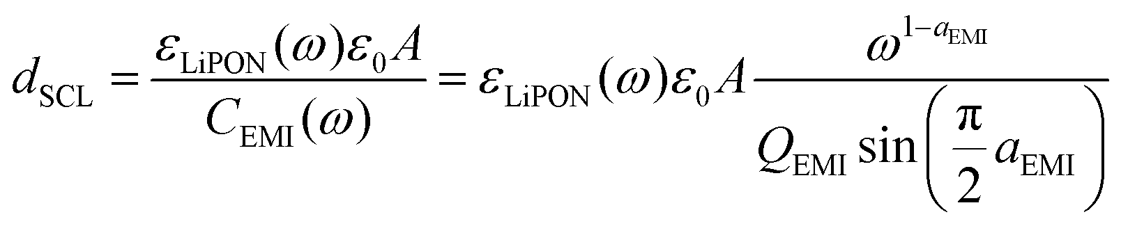
Fig. 2 shows a real image of the final microfabricated devices sharing a single substrate and the electric circuits that were modeled for each diagnostic device according to the physical phenomena happening at the battery components and interfaces. A final electric circuit was built for the thin-film SSB using the numerical values extracted from the electric circuit models of the diagnostic devices.
 | ||
| Fig. 2 Electric circuit models derived for each diagnostics device and thin-film SSBs. Properties of individual layers and interfaces/interphases were extracted from numerical values of color-coded electric circuit elements. For instance, electrical properties of LVO, LiPON and Si were modeled using elements in red, blue and green, respectively. The cathode–electrolyte interphase and the anode–electrolyte interphase were modeled using electric circuit elements shown in orange and purple, respectively. | ||
One of these test devices relies on a metal–insulator–metal arrangement to evaluate the EIS for the insulating electrolyte LiPON. Although the electrolyte–metal interface (EMI) present in such a test device does not exist in the full thin-film SSB, important properties related to the permittivity and ionic resistance of LiPON can be extracted when this interface is decoupled from the rest. During an electrochemical impedance spectroscopy (EIS) measurement, a sinusoidal voltage input creates an electric field such that a majority of Li+ inside LiPON migrates41 towards one of the EMIs when the frequency range is sufficiently small. Li+ arriving at the EMI will be blocked by the metal layer. Electrons flowing inside the metal will reach the same interface for charge neutrality, but will be blocked due to the dielectric properties of the electrolyte, creating a capacitor-like behavior at the EMI (CEMI). The lower the frequency, the more time is allowed for the motion of Li+, so the higher the number of charges near the EMI. On the other metal side, there is a higher concentration of lithium-ion vacancies,42 which also creates a space-charge region in which its thickness denotes the Li+ depletion width.
The anode–metal interface (AMI) and the cathode–metal interface (CMI) will generate space charge layers (SCLs) with distinct electrical properties in comparison to EMI. Li+ migrating inside LVO and/or a-Si during cell charge/discharge will accumulate at their interfaces with the metal layers, while electrons are not blocked. While this type of interface has not been widely studied in the battery field, its behavior under different states-of-charge might reveal important features about the rate of reaction between Li+ and electrons, if the ionic and electronic conductivity at these interfaces remains constant. Ideally, kinetically stable interfaces should maintain their electrical properties, and variations of their conductivities can therefore reflect degradation of batteries during their lifetimes.
The other two remaining interfaces that are created during fabrication are the anode–electrolyte interface (AEI) and the cathode–electrolyte interface (CEI). They are very challenging to be modeled in an electric circuit since intermixing is likely to occur and interphases can be formed during fabrication and under electrochemical cycling. Previous studies have demonstrated that a wide intermixing region between ALD V2O5 and NaPON electrolyte developed in the course of the deposition process.43 In another study, interdiffusion between lithium manganese oxide and LLZO occurred after electrochemical cycling.10 In addition, Li+ diffusion was reported to occur during sputtering when depositing LiPON on V2O5,44 so an interphase is likely to be formed between the cathode and electrolyte thin films in this current work.
Preferably, these interphases will have high ionic conductivities with low electronic conductivities to allow the charge transfer of Li+ from the electrolyte to the anode/cathode and vice versa while suppressing the diffusion of electrons to minimize charge accumulation in those interphase regions and side reactions that could lead to lithium immobilization, resulting then in capacity fading.2,4 They are the most widely studied interfaces in a battery because their local impedances can compromise the total performance of the device. In this work, both AEI and CEI will be modeled as a resistance in parallel to a CPE, in which the resistance is attributed to the charge transfer, and the CPE will inform about their SCLs.
Building full-cell electric circuit model from component EIS signatures
In this work, the investigation of different interfaces and materials that are formed in a SSB and their evolution under different states-of-charge was primarily based on impedance spectroscopy data. For every device fabricated and shown in Fig. 1, an equivalent electric circuit was modeled by considering the materials properties and the mechanisms of charge dynamics under different frequency ranges.32,45–47 Then, the acquired impedance spectra of the measured devices were fitted using the proposed electric circuit models from Fig. 2 for an estimate of the physical properties, like conductivities and relative permittivity values of bulk materials, as well as the width of space-charge regions at interfaces. Electrical properties will be extracted firstly from fitting these equivalent circuits to the measured EISs of the individual layers (called as the diagnostic test devices). Next, these parameters will be transferred to bilayers, and finally assembling the layers and interphases to describe the full cell EIS. Ultimately, the performance and capacity degradation of a full thin-film SSB after 500 cycles will be explained by analysis of the EIS through the lens of the individual components.For each analyzed set of impedance data, the complete frequency range (250 kHz–250 mHz) was fitted to the respective electric circuit model, which is a very important aspect when discussing charge accumulation or depletion of charges at low frequencies. More information about the equations derived for calculation of equivalent impedance, relative permittivity, and width of SCLs can be found in the ESI.†
 | ||
| Fig. 3 (a) Impedance spectrum of LiPON-only diagnostic test device at OCV with the representation of the electric circuit model for data analysis; (b) LiPON ionic conductivity at different applied voltages; (c) relative permittivity of LiPON at different frequencies at OCV; inset: Bode diagram of device at OCV, in which the blue line corresponds to the phase of the total impedance, and the black line is the log of the total impedance modulus; (d) computed space-charge layer (SCL) width at the electrolyte–metal interface (EMI) under different applied voltages calculated at the lowest frequency measurement (250 mHz). | ||
The proposed electric circuit model can also be used for dynamic impedance analysis, i.e., when varying the applied voltage. In this case, for every increase or decrease in the applied bias, an impedance spectrum is acquired, and the parameters of the electric circuit model are used to fit the EIS spectra. Hence, any changes in the LiPON properties or interfacial reactions are reflected on the variation of the electric circuit parameters. Fig. 3b shows the calculation of ionic conductivity of LiPON (σLiPON) at a voltage window of 0–3.6 V, according to the following equation:
 | (1) |
As noted earlier, one potential explanation for CPE behavior is a distribution of material resistance near an interface, but here we exclude this effect due to the small deviations in σLiPON.37 Since bulk properties can now be distinguished from interfacial reactions using the electric circuit model proposed here, the relative permittivity of LiPON (εLiPON) could be computed as a function of frequency:
 | (2a) |
 | (2b) |
SCL width at the two EMIs were monitored over different applied biases. Any changes in the electric circuit parameters of CPEEMI (both a and Q, see eqn (S7) and (S12) on ESI†) result in changes to charge accumulation and interfacial kinetics. The SCL width (dSCL) for thin-film stack devices could then be calculated as follows:
 | (3) |
Therefore, both εLiPON and CEMI will vary as a function of applied bias, which resulted in changes of the dSCL. It was assumed that the width of the Li+ accumulation at one EMI has the same length as Li+ vacancies on the other EMI, even though the metal contacts are different (copper and aluminum), so the width of each SCL in Fig. 3d is an approximate and average result. Adding 2 CPEEMI parameters to the electric circuit model, where each of them would correspond to one EMI, could be more accurate but it would not be possible to fit them without a high degree of correlation, giving rise to ambiguities in data analysis. At low voltages, the SCL is 7–12 nm wide, and towards 3.6 V (vs. Cu) there was an increase of this layer up to 20 nm. Those larger values are consistent with a similar direct measurement of the Cu/LiPON interface using electron holography.53 The increase in the width of the SCL at higher potentials might indicate an eventual LiPON decomposition due to its electrochemical instability above 2.5 V vs. Li/Li+.54,55
 | ||
| Fig. 4 (a) Electric circuit model for the LVO-only test device and impedance spectrum at OCV. (b) Impedance spectrum of Si-only diagnostic device at OCV and the electric circuit model that represents this device. | ||
In contrast to the low-frequency profile of the LiPON-only diagnostic device, which showed a linear relation between real and imaginary impedance components, a second and smaller semi-arc appears in the LVO device. This is explained by the fact that although Li+ are blocked when they accumulate at the CMI, electrons will be free to flow. For the LiPON-only diagnostic test device, charge accumulation at the interfaces took place below 9 kHz, while for LVO it was ∼150 Hz. This is meaningful because it shows that the time constant for LVO is bigger than the LiPON-only device, i.e., a shorter time is needed for Li+ inside LiPON to reach the EMI in comparison to the Li+ transport in LVO.
Indeed, this is confirmed when the resistances of the electric circuit model are used to compute conductivity values for each charged species in LVO. The calculated ionic conductivity was σi,LVO = 0.12 × 10⁻⁶ S cm−1 while the electronic conductivity was σe,LVO = 0.71 × 10⁻⁶ S cm−1. Therefore, σLiPON is about 20 times bigger than σi,LVO, which explains the fast Li+ accumulation at the EMI on LiPON-only diagnostic device. At the minimum measured frequencies (250 mHz), the width of SCL at the CMI was estimated to be (38 ± 6) nm. The SCL width at the CMI is bigger than the value found for EMI since εLVO > εLiPON. Because σe,LVO is ∼6 times larger than σi,LVO, it is possible that, under an EIS experiment, electrons are diffusing from the metal layer to the LVO and reducing more Li+ at the interface.
In Fig. 4b, the impedance spectrum of the Si-only diagnostic test device and the electric circuit model used for its fitting analysis are shown. After a-Si deposition, no Li+ are present, so there is conduction of electrons only (there could be mobile holes from defects, but the impedance spectrum shows no evidence, so they can be considered as minority carriers). Since the deposited a-Si layer is thin (45 nm), the total impedance is reduced so wiring effects are more pronounced, which were modeled using a series inductor.47,57 At low frequencies, the impedance tends to a resistor behavior, with an area-specific resistance of 1.6 Ω cm2. The relative permittivity of a-Si was estimated to be (13 ± 1) at 250 kHz, and the SCL width at the silicon–metal interface could not be modeled in this device due to the pronounced wiring effect previously described.
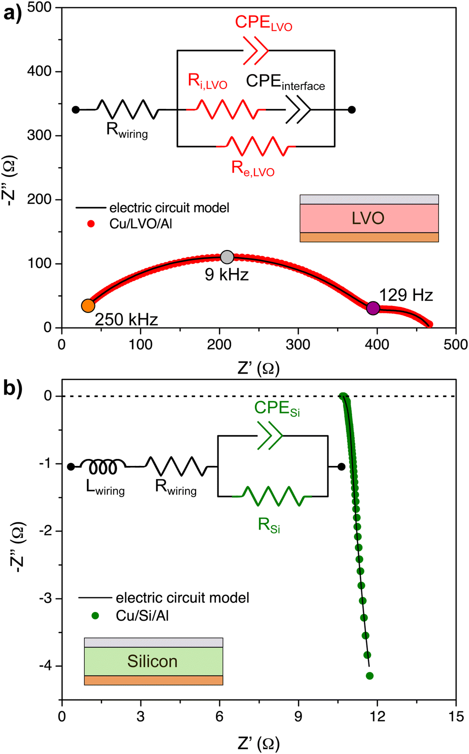
For instance, when LVO is in contact with LiPON, a redistribution of charges is expected to happen, resulting in a CEI formation with distinct electrical properties. Given our interest in understanding the full range of interface behavior, we use the term “interphase” to recognize important aspects such as interfacial reaction, space charge layers, and the reality that these phenomena will cause effectively a finite thickness for the interphase. Our methodology makes it possible to anticipate the properties of this interphase (and SCLs at metal interfaces) from the electric dynamics of the individual LiPON and LVO layers using the electric circuit models from the isolated LVO and LiPON devices. The estimated circuit parameters and network topology for the LiPON-only (shown in blue in Fig. 5c) and LVO-only (shown in red in Fig. 5c) diagnostic devices are incorporated into the larger electric circuit model (Fig. 5c) of the LiPON–LVO diagnostic device for data fitting and analysis as an informed starting point for fitting the LiPON–LVO model to the experimental EIS data for this diagnostic device. Then every parameter is allowed to relax to its appropriate value for best fit to the LiPON–LVO EIS data. The great benefit behind this approach is not only that the isolated LVO and LiPON diagnostic test devices provided initial guesses for the LVO–LiPON device parameters, but rather that the associated parameters are representative of the physical/chemical properties of the LiPON/LVO diagnostic device and that the smaller submodels in Fig. 5c are connected in an arrangement corresponding to physical reality (e.g. EMI/LiPON/CEI/LVO/CMI).
 | ||
| Fig. 5 Impedance spectra of LiPON–LVO diagnostic test device when (a) increasing the voltage, and (b) decreasing the voltage gradient; (c) schematics of the device and the electrically modeled interfaces (and interphase). The values of circuit parameters in blue were taken from the LiPON-only device, and the same applies for circuit parameters in red, taken from the LVO-only device. Circuit parameters in orange are representing the CEI; (d) cyclic voltammogram of LiPON–LVO device; (e) LVO ionic conductivity and (f) LVO electronic conductivity as a function of applied bias. | ||
Hence, charge dynamics and internal impedances can now be fully resolved under different states-of-charge. By increasing the applied voltage in this system, Li+ will be moving from LVO to LiPON. Decreasing the applied voltage will result in Li+ transfer in the opposite direction. Impedance diagrams from Fig. 5a and b show that the LiPON–LVO test device can be modeled using the electric circuit from Fig. 5c, and a significant change in the impedance spectra was observed at voltages higher than 2.7 V. In Fig. 5d, the cyclic voltammetry taken from this device revealed that an electrochemical peak at 3.1 V is observed when the bias is increased that can be ascribed to a partial extraction of Li+ from LVO.26,58 Above 3.3 V, the remaining amount of mobile Li+ inside LVO should be diffusing through the CEI and the LiPON layer, and a current density spike in the mA cm−2 range is noted. The shape and magnitude of this peak is representative of lithium plating59 at the LiPON/Cu interface (EMI), so there should be a convolution of two different reactions happening at the same time: Li+ diffusing out of LVO and Li+ reduction at the EMI. When the applied bias becomes smaller, Li oxidation from EMI and subsequent Li+ diffusion towards the LVO side is observed in the cyclic voltammogram.
While it could be challenging to decouple these two different mechanisms (lithium oxidation/reduction at EMI and Li+ diffusion inside the device), this is now possible using our diagnostics approach. An evaluation of the changes to the electric circuit parameters from the impedance analysis showed, for example, that σi,LVO and σe,LVO vary according to the applied bias in the device. In Fig. 5e, σi,LVO ranges from 1–3 × 10⁻⁶ S cm−1 from 0–3 V. In contrast, the conductivity during the last portion of the sweep is ∼102 times greater. A similar behavior was also observed in electrochemically lithiated V2O5 thin films by Shibuya et al.,60 in which the V2O5 conductivity substantially decreased below 3.0 V vs. Li/Li+ due to a possible irreversible change in its crystal structure.
A kinetically stable interphase should have a good ionic conductivity while being a good electronic insulator to limit further interfacial side reactions.3 In particular, if the impedance is constant and the SCL has a similar thickness at different states-of-charge, then the interphase can be inferred as stable. From the data in Fig. 6a and b, it is evident that the CEI is mostly stable from 0–3 V, despite some fluctuations of its resistance. The SCL is significantly wider than the EMI measured in the LiPON-only device, ranging from 80–160 nm and calculated using eqn (3). It may be caused by a Li+ gradient at the interphase, in which the LiPON-side of LVO has a high concentration of Li+, and heightened by the ready transfer of Li+ between LiPON and LVO, in contrast to the ion-blocking EMIs.61
 | ||
| Fig. 6 Evolution of (a) cathode–electrolyte interphase (CEI) resistance; (b) space-charge layer (SCL) formed at the CEI; (c) SCL at electrolyte–metal interface (EMI); (d) SCL at the cathode–metal interface (CMI) of the LiPON–LVO diagnostic test device. | ||
At higher voltage biases, up to 3.6 V, it seems that the CEI resistance is affected by the charge polarization and the SCL at the CEI drops to small values. This could possibly be explained by the small concentration of Li+ in this region, since the majority of mobile Li+ have diffused towards the EMI at 3.6 V. The average conductivity of the CEI between 0 and 3.6 V can be estimated assuming that its length is equivalent to the SCL (see eqn (S12) on ESI†). In this case, the average σCEI is (0.8 ± 0.2) × 10−6 S cm−1, which is lower than the ionic conductivity of LVO and LiPON. Hence, charge transfer of Li+ in this multiscale process (LVO ↔ CEI ↔ LiPON) can be negatively affected by the sluggish motion of Li+ at the CEI.
The hypothesis of Li oxidation/reduction at the EMI at higher biases is supported by the evolution of the SCL at the EMI seen in Fig. 6c. As the applied voltage was increased, the width of the SCL of LiPON–Cu interface decreased to a sub-nm range, according to calculations based on eqn (3). Above 2 V, it was already very small, which most likely indicates a beginning of LiPON decomposition into Li3PO4 and Li3N.11 Above 3.2 V, lithium reduction occurred. When the applied bias was reversed, Li oxidation reaction takes place at the LiPON/Cu interface and the initial SCL was slowly restored.
Another interesting, and yet infrequently reported interface that was decoupled using this diagnostics approach was the LVO–Al interface (CMI). While increasing the voltage bias, its SCL was mostly stable (20–40 nm wide calculated using eqn (3), also see Fig. 6d), until the last fraction of mobile Li+ from LVO were transferred to CEI and LiPON, which then decreased the width of the SCL to only a few nanometers. When the applied bias was reversed, the SCL slowly increased, and below 1.2 V it was even wider than the initial state (about 3–4 times wider), possibly due to the smaller electronic conductivity of LVO shown in Fig. 5f.
 | ||
| Fig. 7 Impedance spectrum of Si–LiPON diagnostic device (green curve) and the electric circuit model that was built for data analysis. Values of the electric circuit parameters in green were extracted from the Si-only test device, and the blue ones were taken from the LiPON-only test device. The impedance data of LiPON-only device is shown in blue for comparison. | ||
In addition, two resistors were included to represent the electronic flow inside the silicon layer and the eventual ionic flow under equilibrium if there was a spontaneous diffusion of Li+ from the LiPON layer. In the as-deposited state, the electronic resistance was estimated at 1.4 Ω cm2, which agrees with the value found on the Si-only diagnostic device, while the ionic resistance was ∼140 kΩ cm2, confirming that the AEI prevented Li+ from flowing from the LiPON layer during deposition. It is important to note that the deposition sequence is reversed from that of the LiPON/LVO device in that the Si is deposited beneath the LiPON.
The fitting of the electric circuit model to the data from the Si–LiPON device revealed interesting information from the interfaces. The contact between a-Si and copper (anode–metal interface – AMI) created a SCL with an estimated width of (8 ± 1) nm. On the other side of this device, the EMI (in this case, LiPON–Al interface) SCL width was calculated to be (30 ± 2) nm. The data for the LiPON–LVO test device (Fig. 6c) showed that the LiPON–Cu interface was 5 nm-thick, at most. The combination of these results from different auxiliary devices can help us conclude that a thicker SCL exists when LiPON is in contact with Al rather than Cu, and that the average of these two EMI SCLs is 17.5 nm, which is in good agreement with the values in Fig. 3d when studying the interfaces inside the Al/LiPON/Cu diagnostic device.
Describing the EIS of the thin-film SSB full cell
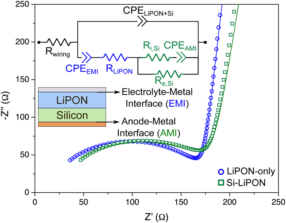
Having previously analyzed the EIS of each diagnostic test device, we can now apply those fitted circuit parameters to an equivalent circuit for the full cell thin film SSB. The circuit, therefore, includes bulk and interfacial parameters, and the knowledge of how the properties evolve under different applied biases. For each parameter added to the circuit in Fig. 8a, the initial values used were extracted from the electric circuits of the diagnostic test devices. This ensures that the impedance analysis is robust, because it considers the different physical properties and chemical reactions happening at the bulk and at different interfaces, at the same time, that are now fully distinguished. | ||
| Fig. 8 (a) Description of the proposed electric circuit model for interpretation of the thin-film SSB impedance analysis; (b) impedance spectra of every auxiliary device at OCV, including the impedance profile of the SSB stack as-deposited; impedance of the SSB after several galvanostatic charge/discharge cycles at 8C recorded at different biases during (c) charge; and (d) discharge half cycles. A discrepancy in the impedance curves at 3.6 V when applying the bias in reverse directions possibly occurred due to relaxation between the charge and discharge measurements. | ||
Fig. 8b shows that the impedance profile of the SSB is a convolution of the impedances of isolated battery components and interfaces, and lacks any discrete features that would allow a decomposition of the spectrum without the systematic approach we have taken. The impedance data in black corresponds to the total impedance of the thin-film SSB after fabrication, at OCV. The Si–LiPON interface (AEI) in that specific EIS curve (as-deposited cell) was not modeled in the electric circuit to avoid over-parameterization, like it was observed on the Si–LiPON device (see Fig. 7). The negligible impedance at the AEI at OCV suggests that little or no reactivity exists between LiPON and a-Si before any electrochemical cycling, which is a characteristic of a passive interface. The LiPON–LVO interface (CEI) of the SSB at OCV had a fitted resistance of 14 Ω cm2, which is comparable to what was found at the LiPON–LVO diagnostic test device (see Fig. 6a), and the ionic resistance of a-Si was within the same order of magnitude (117 kΩ cm2) calculated for the Si–LiPON diagnostic device. Overall, it appears that the subsequent deposition of the anode layers did not alter the LiPON–LVO structure beneath from the state found earlier.
After galvanostatically cycling the battery 545 times at faster rates (8C, which corresponded to a current density of 50 μA cm−2) for the purpose of studying kinetic effects, we analyzed the evolution of the internal impedances as a function of the applied bias. Overall, the total impedance of the SSB before cycling (Fig. 8b, black curve) looks different than any of the impedances after 550 cycles taken at different applied biases (Fig. 8c). While the as-deposited device exhibits a single semi-circle with a low frequency tail, after cycling we find a split into two semicircles at high frequency and a lower angle tail. Furthermore, the impedance data at different biases (Fig. 8c and d) shows that the device properties are not perfectly reversible during each half cycle, and in fact, the two 0 V spectra have different low frequency tails. It is possible that there is a kinetic factor that delays some restoration of the impedance, or this irreversibility in the EIS is indicative of continuing side reactions somewhere in the device.
 | ||
| Fig. 9 Interfacial properties of the thin-film SSB computed from the circuit parameters as a function of applied cell voltage. (a) Space-charge layer (SCL) at the LVO–Al interface; (b) resistance of LVO–LiPON interphase; (c) SCL at the LVO–LiPON interphase. | ||
Interestingly, the width of the LiPON–LVO interphase (CEI) from the full cell (Fig. 9c) agrees with the Li+ gradient observed from an XPS depth profiling data of electrochemically lithiated V2O5–LiPON interface,61 which then validates the deconvolution of impedance profiles performed in this report. A remarkable increase in the CEI resistance with comparison to the uncycled SSB (14 Ω cm2) is shown in Fig. 9b, and a hysteresis in the charge transfer is noted. In particular, when the applied voltage was being increased, this interphase had a resistance that reached 400 Ω cm2 at 1.6 V and the resistance decreased down to 30 Ω cm2 at 3.6 V. When the applied voltage was decreased, the resistance was increased back to around 100 Ω cm2 with a large hysteresis, which was not previously observed for the LiPON–LVO diagnostic device. As we will see next, there is also substantial hysteresis observed for the AEI, and for both cases we can attribute this to a kinetic instability in the full cell which may be connected to the coulombic efficiency of the device.
The ionic conductivity of the CEI in the SSB was estimated to be on the order of 10−9 S cm−1, which is one order of magnitude higher than the value calculated for the LiPON–LVO diagnostic device. Therefore, the difference in the CEI conductivity values predicts a drop in performance after the device begins cycling.
 | ||
| Fig. 10 SSB anode interfaces after cycling. (a) SCL at the Si–Cu interface; (b) resistance of Si–LiPON interphase; (c) SCL of Si–LiPON interphase. | ||
Lastly, the Si–LiPON interphase (AEI) that was previously found to be passive before cycling has become kinetically unstable during charge/discharge cycles. Fig. 10b shows that its resistance reached 4 kΩ cm2 after fully discharging the battery, i.e., when a-Si was delithiated. During the beginning of a charge process, the same interface had a resistance 4 times smaller than the discharge cycle. Hence, the resistance to transfer Li+ across the AEI slowly decreases as the silicon gets more lithiated, and Li+ transfer from Si to LiPON appears to be more favorable at cell voltages above 1.4 V.
The large impedance in the order of kΩ cm2 of the Si–LiPON interphase has also been previously inferred by KPFM analysis coupled with EIS.13 In a similar thin-film SSB stack where LCO was the chosen cathode material, the Si–LiPON interphase impedance was more sensitive to different applied biases than the LCO–LiPON interphase. These results are in agreement with the constant SCL thickness found in our report for LVO–LiPON interphase (Fig. 9c) and the variable SCL width for the AEI (Fig. 10c). Fuller et al. addressed the high impedance at Si–LiPON interphase to a low Li+ diffusivity in amorphous Si, which had caused a Li+ accumulation at this heterojunction. The calculated conductivity of the AEI in our work based on the width of SCL and its local impedance (10−10 S cm−1) is 10 times smaller than the calculated value for the CEI, which corroborates the explanation that Li+ diffusivity is very low at this interphase.
While Fuller et al.13 have estimated the SCL thickness at the AEI to be close to 100 nm, our results showed a much narrower region of less than 10 nm (see Fig. 10c). It is important to emphasize that our impedance measurements were taken after 545 cycles, whereas their measurements are showing initial kinetic behavior of their thin-film SSB for the first 20 cycles. In the following section, we will show that a capacity fading is observed over the charge/discharge cycles, which could be ascribed by the kinetically unstable behavior of the AEI, so variable Si–LiPON SCL thickness as a function of cycle number were somewhat expected.
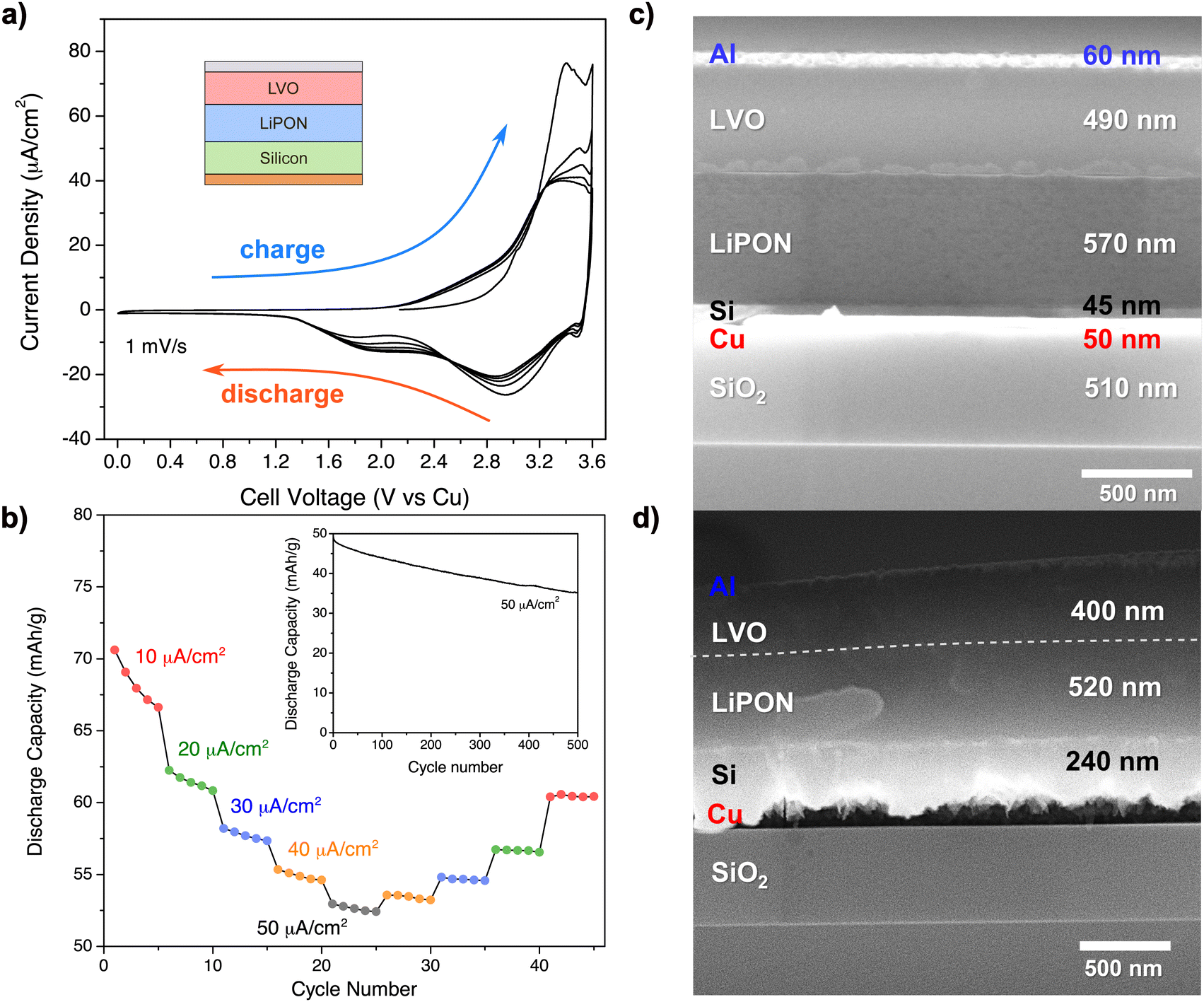 | ||
| Fig. 11 (a) Cyclic voltammogram of a thin-film SSB of the 4 × 4 array, right after deposition. Under the 2-electrode configuration, the copper contact was used both as reference and as a counter electrode. Increasing the total cell voltage refers to charging; (b) discharge capacity under different applied current densities (so different C-rates) for 45 cycles under variable current densities in a fresh, yet uncycled SSB. Inset: Capacity fading at fast charging/discharging for 500 cycles at 8.5C (50 μA cm−2) after cycling 45 times; cross-sectional SEM image of the thin-film SSB atop the SiO2 substrate (c) before any electrochemical cycling; and (d) after 545 total cycles left at a charging state. | ||
On another thin-film SSB that was not yet electrochemically tested from the 4 × 4 array of fabricated devices, a series of 545 galvanostatic charge/discharge cycles was performed under variable C-rates, as shown in Fig. 11b. A larger capacity loss was observed at the initial cycling of the SSB, regardless of the value of the applied currents (e.g. 10 μA cm−2 = 1.7C). From cycle 1 to 45 under variable C-rates, there was a loss of discharge capacity of approximately 15%. Interestingly, the first 45 cycles from the follow-up 500-series at a high C-rate of 8.5C (50 μA cm−2) resulted in a discharge capacity loss of 8%. This evidence shows that fast charging was not the only factor contributing to the device performance below the expected. Apparently, problems occurring at the beginning of the battery lifetime have caused irreversible changes on the device.
SEM analysis of the fractured cross section of an uncycled, as-deposited thin-film SSB (Fig. 11c) revealed that most of the interfaces were smooth after completion of the fabrication process, besides some irregular patterns that were noted at the LVO–LiPON interface possibly due to the fracture, or because of an interphase that formed during the deposition of the LVO onto the LiPON. The interfaces of the full stack looked completely different after 545 cycles, here shown in a charged state (Fig. 11d). There is an evident volume expansion of silicon (about 4.33 times) when it gets lithiated that is in accordance with the literature62 which had possibly caused a contact loss between Si and Cu, and a LiPON decomposition at AEI63 could have caused shrinking of 9% of the total LiPON layer. LVO had an 18% thickness reduction, but this could be due to Li+ extraction from its structure.
Overall, electrochemical measurements and SEM images are in accordance with the results observed from the impedance analysis. The Si–LiPON interphase was not included in the electric circuit models of the Si–LiPON diagnostic device, nor in the full SSB before cycling, because of its negligible impedance. Our hypothesis for this case was that the Si–LiPON interphase was passive during/after fabrication, and the SEM images shown in Fig. 11c showed a smooth contact between Si and LiPON that agrees with our premise.
After cycling, the SEM in Fig. 11d revealed a volume expansion of LixSi at a charged state that drastically affected the stability of the Si–LiPON interphase, which was confirmed by the capacity fading observed on electrochemical measurements in Fig. 11a and b. The calculation of the AEI conductivity from the impedance analysis reinforces the argument that this interface was a major source of battery degradation. The direct relationship between cell performance and interface kinetics in this report was only possible due to our diagnostics protocol for systematic decoupling of internal impedances in a SSB.
Prognosis
It is perhaps well known that a battery is more than the sum of its parts. The properties of interfaces/interphases are important parameters for device performance, and the fact that many properties vary with ion concentration further complicates the analysis. By using thin film deposition to break up the battery into component parts, and analyzing each in turn, we find that changes in material properties and interphases can be fully accounted for. Furthermore, these fitted parameters do not become wild or highly correlated when examining the full cell, implying that the model is not overfitting the data, and verifies the hypothesis that the thin film full cell can be described by its component parts, once they are all accounted for.The use of diagnostic devices to deconvolute impedances in a SSB also proposes that in situ experiments can be done using this technique. For example, internal impedances can be spatially resolved by performing a 2D-mapping of a SSB using KPFM analysis, to probe the behavior of charge transfer at interfaces in different locations. For the case of crystalline materials and/or interfaces, coupling XRD measurements with impedance analysis over different states-of-charge can evaluate the mobility of majority charge carriers at grain boundaries versus in bulk. And, in general, this protocol using individual and isolated test devices can provide comparisons of battery health while simultaneously performing morphological, structural, mechanical, and electrochemical characterization techniques on sibling devices.
While a complete study of interface kinetics in a SSB still requires in situ experimental techniques such as SEM (scanning electron microscopy), XPS, ToF-SIMS (time-of-flight secondary ion mass spectroscopy), KPFM, AES (Auger electron spectroscopy), RBS (Rutherford backscattering spectroscopy), and/or TEM,10,27,64–68 an electrochemical impedance analysis coupled with an appropriate system of devices can reveal features of the interfaces during cycling, as well as indicate possible issues occurring during processing that were yet unreported. Hence, a direct, non-destructive measurement of the physical properties of interfaces is now feasible for a wider range of thin-film devices, which can substantially improve the design of next-generation ionic devices.25,69
For the first time, the kinetics of interfaces in a SSB was monitored and reported from impedance analysis to diagnose full cell performance and degradation during fast cycling. The simple premise of decoupling bulk and interfacial internal impedances by building single and bilayer devices, deriving physics-based electric circuit models for every layer (and interface) individually, and combining their circuit parameters into a robust and complete electric circuit for the full battery, has proven to work successfully. Circuit parameters from the diagnostic test devices fully explain the behavior of the full cell, with minimal drift in the fitted values from test device to full cell.
In the previous sections, we have shown that equivalent circuit analysis can provide models and parameters that are transferable from simple systems to complex ones. For instance, important material properties were calculated under different applied biases, such as the relative permittivity of the active materials, conductivities of bulk layers and across at interphases, and the width of space-charge regions at heterojunctions. Variations in these material properties can be explained by well-known dynamics in solid-state batteries, and provide quantitative measurements of parameters necessary for advanced modeling of electrochemical systems.
There are several beneficial impacts to the field of electrochemical devices coming from these calculated properties. Conductivity measurements at interfaces can determine whether protective layers must be incorporated to adjust the electrical properties of interfaces closer to ideal values. Also, different combinations of promising materials can now be tested using this diagnostic protocol to investigate compatibility. And, more broadly, the calculated values of materials properties can now be included in computational simulations for a better prediction of device performance.
As it was mentioned during this report, simple materials with simple interfaces were studied as a proof-of-concept. Adding materials with more complex structures like grain boundaries, or intrinsic tortuosity, porosity, and voids that exist in particulate SSBs will require extra assumptions to be made when building the electric circuit models. The inclusion of inactive materials such as carbon black will also add more challenges to fully deconvolute the internal impedances, so additional diagnostic test devices may be required to be fabricated and studied. Lastly, thin-film batteries with unique architectures like AAO-nanopore arrays for fabrication of 3D thin-film SSBs70 will have to be carefully studied because the electric field lines are not as uniform as they are in planar batteries, so the calculations of space-charge layers have to be derived considering the nature of their architectures.
Since we were evaluating the effect of interfaces in thin-film batteries, we suggested a fabrication approach using shadow masks that would create the individual devices and the full cell all together. But this methodology can be transferred to conventional solid-state batteries. For instance, a cathode side of a particulate-based solid-state battery has more intrinsic interfaces than a thin-film one. Using our new methodology, one could fabricate the following devices as pellets that would represent each cathode component:
– Current collector (CC)/active material (cathode)/CC
– CC/solid electrolyte/CC
– CC/conductive additive (such as carbon)/CC
This approach would enable, for example, the extraction of electronic and ionic properties of individual cathode components and the evaluation of their stability with current collectors separately, and then further analysis would go towards the fabrication of new pellets that correspond to permutations of these components to analyze individual interfaces:
– CC/cathode/solid electrolyte/CC
– CC/cathode/conductive additive/CC
– CC/solid electrolyte/conductive additive/CC
– CC/cathode/solid electrolyte/conductive additive/CC
Using these test devices, the electrical response of internal components in a cathode composite could be individually studied. However, that there are considerations to take into account when moving from monolithic films to these particulate-based systems for the design of electric circuit models to represent them with fidelity. For instance, our hypothesis is that there might be necessary to fabricate different test devices under a range of applied pressure, so that a direct relationship between changes in the electrical properties of internal cathode interfaces and applied pressure can be made. Grain boundaries were not present in our system, but we are aware that conduction of charges at those boundaries might be preferrable in many materials, which would create another possible path for both ions and electrons to flow during operation of the battery. More so, there might be accumulation of charges at the grain boundaries, which could affect the overall performance of the cells. Hence, the inclusion of grain boundaries in the electric circuit model would have to incorporate the electrical resistance of them and also any possible charge accumulation that might exist, which can be properly modeled using a resistor in parallel to a CPE, in series with the ionic resistance of the material. Combining such impedance measurements with other characterization techniques, such as TEM and XRD, could reveal the grain sizes and the reactivity of their boundaries, which could help on the interpretation of the electrical analysis and further improve the electric circuit model.
Although this report only performs diagnostics of simple thin-film SSBs, the challenges previously described for more complex systems only require some understanding of the structure of the system to include important chemical and physical properties into the electric circuit modeling. Hence, the benefits of using this diagnostics protocol for other battery systems can potentially increase the understanding of the battery community in local interfaces and impedances and their consequences for capacity retention, cell degradation and compatibility of promising materials.
Conclusions
The possibility of designing novel SSB architectures for an improvement of the energy and power densities strictly depends on maximizing charge transfer across the different interfaces existing in this unique and complex system. Interface (and interphase) kinetics were proven to affect the overall performance of thin-film SSBs using the new diagnostics protocol presented in this work. The additional information obtained by careful experimental design leads to conclusive decisions about which interfaces to focus on and provides baseline information to control against when designing novel interphase control techniques. By combination of impedance spectroscopy analysis, conventional electrochemical measurements, and a singular device fabrication methodology, we provided a systematic deconvolution of charge dynamics in the bulk and at interfaces of a thin-film SSB.Patterned auxiliary devices that represented isolated battery components were used to build electric circuit models that enabled a realistic interpretation of the electrochemical reactions and properties of materials in these devices. Accumulation of charges at interfaces and conductivities of Li+ and electrons across different layers were monitored at different states-of-charge, and, for instance, a space-charge layer in the range of 100 nm was observed at the cathode–metal interface and the cathode–electrolyte interphase after completion of the fabrication process. The anode–electrolyte interface was found to be stable only before cycling using both impedance analysis and cross-sectional SEM imaging.
The determination of how the interfaces changed with different applied voltages was only possible by the implementation of the auxiliary device diagnostics approach. For instance, the LVO–LiPON interphase was found to be resistive to Li+ transfer, especially during charging, but the LiPON–Si interphase was 10 times more resistive. Also, an increase in the space-charge region width specifically at the Si–Cu interface indicated a possible contact loss caused by the anode volume expansion.
The information extracted from the auxiliary devices served as initial input for the electric circuit model of the full cell thin-film SSB. A 15% decrease in capacity was observed as a function of charge/discharge cycles during the first 45 cycles, which was correlated to an effect of the kinetically unstable Si–LiPON interphase. The capacity fading observed as a function of number of cycles is a direct evidence of side reactions. The impedance analysis of the Al–LVO–LiPON–Cu diagnostic device showed that the as-deposited CEI conductivity was, in average, 8 × 10⁻⁷ S cm−1. In addition, the as-deposited AEI was thermodynamically stable. On the other hand, our calculated values of electrical conductivity at the CEI and AEI after cycling (10−9 and 10−10 S cm−1, respectively, in average) were orders of magnitude smaller than their pristine states, confirming that a slow charge transfer reaction is expected in these interphases during operation.
The identification of the AEI as the main performance limiting factor using our novel methodology for fabrication of diagnostic devices combined with EIS measurements has also been previously confirmed by reported KPFM measurements from the literature. Therefore, it is now possible to use a non-destructive technique, such as impedance analysis, to extract important information about fundamental science of thin-film batteries and evaluate performance diagnostics of electrochemical devices.
Hence, this work demonstrated how important it is to incorporate diagnostics of batteries to understand possible fabrication inconsistencies and kinetic behavior during their operation. For the particular choice of materials studied in this prototype, volume expansion of silicon upon lithiation caused contact loss with the current collector and a kinetically unstable Si–LiPON interphase was present during cycling of the battery. In the future, different artificial interfaces could be deposited using the methodology described here between silicon and LiPON to provide mechanical strength while maintaining a reasonable low ionic resistivity for further battery operation without loss of capacity. Interfacial stabilization of the cathode–electrolyte interphase has also proven to be necessary to improve charge transfer. We believe, therefore, that the combination of our robust diagnostics protocol and interfacial engineering will enable the implementation of more complex architectures for the next generation of SSBs.
Author contributions
V. C. F. contributed with conceptualization, investigation, formal analysis, methodology, validation and writing – original draft – of the research output. S. B. L. contributed with writing – review and editing. G. W. R. contributed with conceptualization, supervision and writing – review and editing. D. M. S. contributed with conceptualization, supervision, methodology and writing – review and editing.Data availability
Data for this article, including fitting parameters of equivalent circuit models, electrochemical impedance spectroscopy, cyclic voltammetry and galvanostatic charge–discharge measurements are available at the Digital Repository at the University of Maryland (DRUM) at https://hdl.handle.net/1903/33158. DRUM is a long-term, open-access repository managed and maintained by the University of Maryland Libraries.Conflicts of interest
There are no conflicts to declare.Acknowledgements
This work was supported by the U.S. Department of Energy, Office of Science, Office of Basic Energy Sciences, under Grant DE-SC0021070. The authors also acknowledge the support of the Maryland NanoCenter and its FabLab.References
- S. Lou, F. Zhang, C. Fu, M. Chen, Y. Ma, G. Yin and J. Wang, Adv. Mater., 2021, 33, 2000721 CrossRef CAS PubMed.
- C. Chen, M. Jiang, T. Zhou, L. Raijmakers, E. Vezhlev, B. Wu, T. U. Schülli, D. L. Danilov, Y. Wei, R. Eichel and P. H. L. Notten, Adv. Energy Mater., 2021, 11, 2003939 CrossRef CAS.
- T. Famprikis, P. Canepa, J. A. Dawson, M. S. Islam and C. Masquelier, Nat. Mater., 2019, 18, 1278–1291 CrossRef CAS PubMed.
- Y. Xiao, Y. Wang, S.-H. Bo, J. C. Kim, L. J. Miara and G. Ceder, Nat. Rev. Mater., 2019, 5, 105–126 CrossRef.
- K. Leung, A. J. Pearse, A. A. Talin, E. J. Fuller, G. W. Rubloff and N. A. Modine, ChemSusChem, 2018, 11, 1956–1969 CrossRef CAS PubMed.
- C.-F. Xiao, J. H. Kim, S.-H. Cho, Y. C. Park, M. J. Kim, K.-B. Chung, S.-G. Yoon, J.-W. Jung, I.-D. Kim and H.-S. Kim, ACS Nano, 2021, 15, 4561–4575 CrossRef CAS PubMed.
- J. Kasnatscheew, R. Wagner, M. Winter and I. Cekic-Laskovic, Top. Curr. Chem., 2018, 376, 16 CrossRef PubMed.
- F. S. Gittleson and F. El Gabaly, Nano Lett., 2017, 17, 6974–6982 CrossRef CAS PubMed.
- Z. Wang, D. Santhanagopalan, W. Zhang, F. Wang, H. L. Xin, K. He, J. Li, N. Dudney and Y. S. Meng, Nano Lett., 2016, 16, 3760–3767 CrossRef CAS PubMed.
- A. A. Delluva, J. Dudoff, G. Teeter and A. Holewinski, ACS Appl. Mater. Interfaces, 2020, 12, 24992–24999 Search PubMed.
- D. Cheng, T. A. Wynn, X. Wang, S. Wang, M. Zhang, R. Shimizu, S. Bai, H. Nguyen, C. Fang, M. Kim, W. Li, B. Lu, S. J. Kim and Y. S. Meng, Joule, 2020, 4, 2484–2500 Search PubMed.
- Y. Qi, M. W. Swift, E. J. Fuller and A. A. Talin, MRS Bull., 2023, 48, 1239–1246 Search PubMed.
- E. J. Fuller, E. Strelcov, J. L. Weaver, M. W. Swift, J. D. Sugar, A. Kolmakov, N. Zhitenev, J. J. McClelland, Y. Qi, J. A. Dura and A. A. Talin, ACS Energy Lett., 2021, 6, 3944–3951 CrossRef CAS.
- N. Ogihara, Y. Itou, T. Sasaki and Y. Takeuchi, J. Phys. Chem. C, 2015, 119, 4612–4619 CrossRef CAS.
- T. Momma, T. Yokoshima, H. Nara, Y. Gima and T. Osaka, Electrochim. Acta, 2014, 131, 195–201 CrossRef CAS.
- K. L. Browning, R. L. Sacci and G. M. Veith, J. Electrochem. Soc., 2017, 164, A580–A586 CrossRef CAS.
- S. Kremer, R. Rekers, U. Sigar, J. Becker, J. Schubert, J. K. Eckhardt, A. Bielefeld, F. H. Richter and J. Janek, ACS Appl. Mater. Interfaces, 2024, 16, 44236–44248 Search PubMed.
- J. Huang, Z. Li and J. Zhang, J. Power Sources, 2015, 273, 1098–1102 CrossRef CAS.
- L. Teo, V. R. Subramanian and D. T. Schwartz, J. Electrochem. Soc., 2021, 168, 010526 CrossRef CAS.
- Y. Choi and S. Pyun, Solid State Ionics, 1997, 99, 173–183 CrossRef CAS.
- H. Watanabe, S. Omoto, Y. Hoshi, I. Shitanda and M. Itagaki, J. Power Sources, 2021, 507, 230258 CrossRef CAS.
- M. D. Murbach, V. W. Hu and D. T. Schwartz, J. Electrochem. Soc., 2018, 165, A2758–A2765 CrossRef CAS.
- R. Koerver, F. Walther, I. Aygün, J. Sann, C. Dietrich, W. G. Zeier and J. Janek, J. Mater. Chem. A, 2017, 5, 22750–22760 RSC.
- N. Meddings, M. Heinrich, F. Overney, J.-S. Lee, V. Ruiz, E. Napolitano, S. Seitz, G. Hinds, R. Raccichini, M. Gaberšček and J. Park, J. Power Sources, 2020, 480, 228742 CrossRef CAS.
- M. Gaberšček, Nat. Commun., 2021, 12, 6513 CrossRef PubMed.
- V. C. Ferrari, N. S. Kim, S. B. Lee, G. W. Rubloff and D. M. Stewart, J. Mater. Chem. A, 2022, 10, 12518–12531 RSC.
- D. Santhanagopalan, D. Qian, T. McGilvray, Z. Wang, F. Wang, F. Camino, J. Graetz, N. Dudney and Y. S. Meng, J. Phys. Chem. Lett., 2014, 5, 298–303 CrossRef CAS PubMed.
- J. Bates, G. Gruzalski, N. Dudney, C. Luck and X. Yu, Solid State Ionics, 1994, 70–71, 619–628 CrossRef CAS.
- H. Wang, Y. Song, V. C. Ferrari, N. S. Kim, S. B. Lee, P. Albertus, G. Rubloff and D. M. Stewart, ACS Appl. Mater. Interfaces, 2023, 15, 40409–40418 CrossRef CAS PubMed.
- A. J. Pearse, T. E. Schmitt, E. J. Fuller, F. El-Gabaly, C.-F. Lin, K. Gerasopoulos, A. C. Kozen, A. A. Talin, G. Rubloff and K. E. Gregorczyk, Chem. Mater., 2017, 29, 3740–3753 CrossRef CAS.
- P. Zhu, D. Gastol, J. Marshall, R. Sommerville, V. Goodship and E. Kendrick, J. Power Sources, 2021, 485, 229321 CrossRef CAS.
- R. A. Huggins, Ionics, 2002, 8, 300–313 CrossRef CAS.
- C. Zhu, R. E. Usiskin, Y. Yu and J. Maier, Science, 2017, 358, 1400 CrossRef CAS PubMed.
- G. J. Brug, A. L. G. van den Eeden, M. Sluyters-Rehbach and J. H. Sluyters, J. Electroanal. Chem. Interfacial Electrochem., 1984, 176, 275–295 CrossRef CAS.
- K. S. Cole and R. H. Cole, J. Chem. Phys., 1941, 9, 341–351 CrossRef CAS.
- L. Young, Trans. Faraday Soc., 1955, 51, 1250–1260 RSC.
- B. Hirschorn, M. E. Orazem, B. Tribollet, V. Vivier, I. Frateur and M. Musiani, J. Electrochem. Soc., 2010, 157, C452 CrossRef CAS.
- L. Le Van-Jodin, F. Ducroquet, F. Sabary and I. Chevalier, Solid State Ionics, 2013, 253, 151–156 CrossRef CAS.
- L. Le Van-Jodin, A. Claudel, C. Secouard, F. Sabary, J.-P. Barnes and S. Martin, Electrochim. Acta, 2018, 259, 742–751 CrossRef CAS.
- S. Nowak, F. Berkemeier and G. Schmitz, J. Power Sources, 2015, 275, 144–150 CrossRef CAS.
- A. R. Genreith-Schriever and R. A. De Souza, Phys. Rev. B, 2016, 94, 224304 CrossRef.
- M. W. Swift and Y. Qi, Phys. Rev. Lett., 2019, 122, 167701 CrossRef PubMed.
- R. B. Nuwayhid, A. C. Kozen, D. M. Long, K. Ahuja, G. W. Rubloff and K. E. Gregorczyk, ACS Appl. Mater. Interfaces, 2023, 15, 24271–24283 CrossRef CAS PubMed.
- Z. Warecki, V. C. Ferrari, D. A. Robinson, J. D. Sugar, J. Lee, A. V. Ievlev, N. S. Kim, D. M. Stewart, S. B. Lee, P. Albertus, G. Rubloff and A. A. Talin, ACS Energy Lett., 2024, 9, 2065–2074 Search PubMed.
- M. Gaberšček, Curr. Opin. Electrochem., 2022, 32, 100917 CrossRef.
- R. R. Gaddam, L. Katzenmeier, X. Lamprecht and A. S. Bandarenka, Phys. Chem. Chem. Phys., 2021, 23, 12926–12944 RSC.
- R. M. Nelms and B. J. Tatarchuk, IEEE Trans. Ind. Appl., 2001, 37, 4–9 CrossRef.
- J. D. LaCoste, A. Zakutayev and L. Fei, J. Phys. Chem. C, 2021, 125, 3651–3667 CrossRef CAS.
- K. Ahuja, V. Sallaz, R. B. Nuwayhid, F. Voiron, P. McCluskey, G. W. Rubloff and K. E. Gregorczyk, J. Power Sources, 2023, 575, 233056 CrossRef CAS.
- T. Tsuruoka, J. Su and K. Terabe, ACS Appl. Electron. Mater., 2020, 2, 2788–2797 CrossRef CAS.
- A. López-Grande, G. C. Mather and F. Muñoz, J. Mater. Chem. A, 2023, 11, 12282–12296 RSC.
- Z.-W. Fu, W.-Y. Liu, C.-L. Li, Q.-Z. Qin, Y. Yao and F. Lu, Appl. Phys. Lett., 2003, 83, 5008–5010 CrossRef CAS.
- Y. Aizawa, K. Yamamoto, T. Sato, H. Murata, R. Yoshida, C. A. J. Fisher, T. Kato, Y. Iriyama and T. Hirayama, Ultramicroscopy, 2017, 178, 20–26 CrossRef CAS PubMed.
- Y. Zhu, J. C. Gonzalez-Rosillo, M. Balaish, Z. D. Hood, K. J. Kim and J. L. M. Rupp, Nat. Rev. Mater., 2020, 6, 313–331 CrossRef.
- M. W. Swift, J. W. Swift and Y. Qi, Nat. Comput. Sci., 2021, 1, 212–220 CrossRef PubMed.
- J. Jamnik and J. Maier, J. Electrochem. Soc., 1999, 146, 4183–4188 CrossRef CAS.
- H. Nara, T. Yokoshima and T. Osaka, Curr. Opin. Electrochem., 2020, 20, 66–77 CrossRef CAS.
- C. Navone, R. Baddour-Hadjean, J. P. Pereira-Ramos and R. Salot, Electrochim. Acta, 2008, 53, 3329–3336 CrossRef CAS.
- W. C. West, J. F. Whitacre and J. R. Lim, J. Power Sources, 2004, 126, 134–138 CrossRef CAS.
- M. Shibuya, S. Yamamura, T. Matsue and I. Uchida, Chem. Lett., 1995, 749–750 CrossRef CAS.
- Z. Levy, V. C. Ferrari, P. Rosas, M. J. Walker, K. Duddella, M. Haseman, D. Stewart, G. Rubloff and L. J. Brillson, ACS Appl. Energy Mater., 2023, 6, 4538–4548 Search PubMed.
- R. Koerver, W. Zhang, L. De Biasi, S. Schweidler, A. O. Kondrakov, S. Kolling, T. Brezesinski, P. Hartmann, W. G. Zeier and J. Janek, Energy Environ. Sci., 2018, 11, 2142–2158 RSC.
- H.-K. Tian, A. Chakraborty, A. A. Talin, P. Eisenlohr and Y. Qi, J. Electrochem. Soc., 2020, 167, 090541 CrossRef CAS.
- Z. D. Hood, X. Chen, R. L. Sacci, X. Liu, G. M. Veith, Y. Mo, J. Niu, N. J. Dudney and M. Chi, Nano Lett., 2021, 21, 151–157 CrossRef CAS PubMed.
- A. J. Pearse, E. Gillette, S. B. Lee and G. W. Rubloff, Phys. Chem. Chem. Phys., 2016, 18, 19093–19102 RSC.
- S. Wang, H. Xu, W. Li, A. Dolocan and A. Manthiram, J. Am. Chem. Soc., 2018, 140, 250–257 CrossRef CAS PubMed.
- E. E. Horopanitis, G. Perentzis, I. Samaras, T. Dikonimos-Makris, N. Lisi and L. Papadimitriou, J. Solid State Electrochem., 2003, 8, 55–58 CrossRef CAS.
- K. Morita, B. Tsuchiya, J. Ohnishi, T. Yamamoto, Y. Iriyama, H. Tsuchida, T. Majima and K. Suzuki, Nucl. Instrum. Methods Phys. Res., Sect. B, 2018, 426, 30–33 CrossRef CAS.
- Y. Qi, Nat. Energy, 2023, 8, 1307–1308 Search PubMed.
- C. Liu, E. I. Gillette, X. Chen, A. J. Pearse, A. C. Kozen, M. A. Schroeder, K. E. Gregorczyk, S. B. Lee and G. W. Rubloff, Nat. Nanotechnol., 2014, 9, 1031–1039 CrossRef CAS PubMed.
Footnotes |
| † Electronic supplementary information (ESI) available. See DOI: https://doi.org/10.1039/d4ee03915g |
| ‡ Present address: Chemical Sciences and Engineering Division, Argonne National Laboratory, Lemont, Illinois, 60439, USA. E-mail: vcastagnaferrari@anl.gov |
| This journal is © The Royal Society of Chemistry 2025 |