
 Open Access Article
 This Open Access Article is licensed under a
 Creative Commons Attribution 3.0 Unported Licence
A digital laboratory with a modular measurement system and standardized data format†
Kazunori
Nishio
 *a,
Akira
Aiba
a,
Kei
Takihara
a,
Yota
Suzuki
a,
Ryo
Nakayama
b,
Shigeru
Kobayashi
b,
Akira
Abe
c,
Haruki
Baba
c,
Shinichi
Katagiri
c,
Kazuki
Omoto
d,
Kazuki
Ito
e,
Ryota
Shimizu
b and
Taro
Hitosugi
*ab
*a,
Akira
Aiba
a,
Kei
Takihara
a,
Yota
Suzuki
a,
Ryo
Nakayama
b,
Shigeru
Kobayashi
b,
Akira
Abe
c,
Haruki
Baba
c,
Shinichi
Katagiri
c,
Kazuki
Omoto
d,
Kazuki
Ito
e,
Ryota
Shimizu
b and
Taro
Hitosugi
*ab
aSchool of Materials and Chemical Technology, Institute of Science Tokyo, Kanagawa 226-0026, Japan. E-mail: nishio.k.f0ca@m.isct.ac.jp
bDepartment of Chemistry, The University of Tokyo, Tokyo 113-0033, Japan. E-mail: hitosugi@g.ecc.u-tokyo.ac.jp
cJEOL Ltd., Tokyo 196-8558, Japan
dProduct Division, Rigaku Corporation, Tokyo 196-8666, Japan
eX-ray Research Laboratory, Rigaku Corporation, Tokyo 196-8666, Japan
First published on 14th May 2025
Abstract
Machine learning, robotics, and data are the keys for accelerating the discovery of new materials. While collecting more data is essential, the experimental processes remain a bottleneck. In this study, we constructed a digital laboratory by interconnecting apparatuses using robots to collect experimental data (synthesis processes and measured physical properties, including measurement conditions) for solid materials research. A variety of modular experimental instruments are physically interconnected, enabling fully automated processes from material synthesis to measurement and analysis. The data from each measurement instrument are outputted in an XML format, namely MaiML, and collected in a cloud-based database. In addition, the data are analyzed by software and utilized on the cloud. Using this system, we demonstrate an autonomous synthesis of high-quality LiCoO2 (001) thin films. The system maximized the X-ray diffraction peak-intensity ratio of LiCoO2 (001) thin films using Bayesian optimization. This system demonstrates advanced automatic and autonomous material synthesis for data- and robot-driven materials science.
1 Introduction
Much effort has long been devoted to exploring new solid materials through heuristic approaches. Rational synthesis using the theoretical prediction of compounds and their synthetic pathways has been employed to efficiently explore the vast search space.1 In addition, the automation and parallelization of synthesis through high-throughput methods such as combinatorial approaches have advanced.2,3Recently, machine learning and robotics opened new avenues for automatic and autonomous experiments.4–7 Experimental laboratories are significantly transforming; laboratories are not merely the places to house experimental instruments but rather the factories for producing materials and data, where experimental equipment operates as a system. By delegating repetitive experimental tasks to robot systems controlled by machine learning, it is feasible to synthesize, measure, and analyse a vast number of samples, thereby generating extensive data. This data- and robot-driven science, in conjunction with the standardization of materials synthesis and measurement instruments, and the automation of data collection, will significantly change how we conduct research.
Data- and robot-driven science highlights the importance of the variety and quantity of available data. It is critical to collect all data in an independent and accessible data format.4 The amount of data significantly increases due to conducting multifaceted analytical evaluations of each synthesized sample. Data are categorized into three main types: (1) process data during material synthesis, such as temperature and atmosphere (including synthesis conditions specified by computers or humans and the real-time results monitored by various sensors), (2) measurement conditions for structural and physical property measurements and (3) measurement results.
Robots enable automated synthesis and measurements of a wide variety of properties and facilitate multifaceted data acquisition. Simultaneously, as the methods for materials synthesis and structural/physical property measurements become more diverse, acquiring data by integrating instruments manufactured by different companies is required. Therefore, it is essential to modularize and physically interconnect these instruments. Modularized instruments have been prominent in the field of liquid sample handling and the life sciences. For example, standardization using 96 well plates is progressing.8
In recent years, modularization and standardization of solid materials research for powders have been reported (ASTRAL9 and A-Lab10). For thin-film materials, a modular robotic platform, namely Ada, has been developed for accelerated discovery of organic and inorganic materials relevant to materials sciences and clean energy technologies.11 However, this modularization and standardization are still rudimentary. Two main factors are responsible for this lag. The first is the diversity of sample and sample holder shapes, with no established standards for shapes and sizes. Solids exhibit a variety of physical shapes, including powder and bulk forms. Therefore, standardizing sample shapes and sample holders is crucial for modularizing each instrument. The standardized shapes and holders can expand to diverse material systems such as ceramics, polymers, and composites.
The second reason is the lack of a unified format for measurement data, which complicates the data collection. Traditionally, data from measurement instruments manufactured by different companies have been output in various formats, necessitating users to convert these formats themselves. This situation underscores the need for a standardized format. The Japan Analytical Instruments Manufacturers Association (JAIMA), in collaboration with its member companies and the Ministry of Economy, Trade and Industry (METI), established a data format called the Measurement Analysis Instrument Markup Language (MaiML).12,13 In May 2024, MaiML was registered as a Japanese Industrial Standard (JIS) (JIS K0200). Therefore, it is possible to demonstrate the collection and utilization of data using this standardized format.
In this study, we developed a digital laboratory (dLab) that fully automates the material synthesis and structural/physical property evaluation of thin-film samples. Data in MaiML format are automatically collected, analyzed, and utilized for autonomous materials exploration. In dLab, various modular experimental instruments are physically interconnected, allowing for complete automation from thin-film material synthesis to a wide variety of measurements for surface microstructures, X-ray diffraction patterns, Raman spectra, electrical conductivity, and optical transmittance.
Details about the size of the thin-film samples and sample holders, methods of physical connection of modular instruments, and communication protocols for interconnecting the modular instruments are disclosed in the ESI.† Measurement data are collected in a cloud-based database in MaiML format and analyzed using cloud-based software. The results of this analysis, combined with the synthesis condition datasets, are fed back into machine learning models to predict the following synthesis conditions, enabling the robot to conduct material exploration autonomously.
Specifically, this study demonstrates the autonomous synthesis of LiCoO2 (001) thin films and their structural evaluation via X-ray diffraction pattern measurements. LiCoO2 is a representative positive-electrode material for Li-ion batteries,14 with an α-NaFeO2-type layered rock-salt structure.15 By focusing on the ratio of the X-ray diffraction peak intensities of 003 and 006, we autonomously maximized the crystallinity of LiCoO2 (001) thin films.
2 Experimental methods
2.1 Overview
The dLab consists of two systems: one that integrates experimental instruments to perform automated materials synthesis and measurements (Fig. 1) and the other that handles data collection and analysis. The former comprises a group of modularized instruments responsible for materials synthesis and physical property measurements as follows.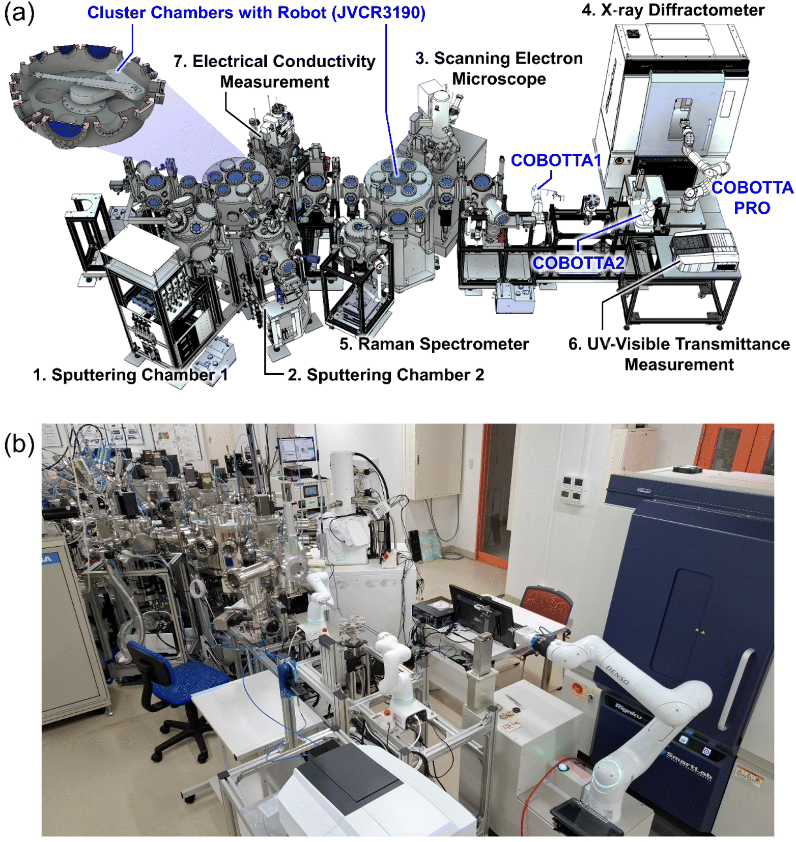 | ||
| Fig. 1 (a) Overall diagram of the system for automated and autonomous experiments. The modularized synthesis instruments (sputtering deposition system) are connected to various modularized measurement and analysis instruments. Details regarding the sample holder shape and the communication protocol used when connecting each module are publicly available.12 (b) A photograph of the system. | ||
(1) Sputtering chamber 1 (PASCAL CO., LTD): thin-film deposition by RF magnetron sputtering with three sputtering guns.
(2) Sputtering chamber 2 (PASCAL CO., LTD): metal thin-film deposition by DC magnetron sputtering with four sputtering guns.
(3) Scanning electron microscope (JEOL JSM-IT700HR/LA): surface imaging and elemental compositional analysis (energy dispersive X-ray spectroscopy, EDS).
(4) X-ray diffractometer (Rigaku SmartLab): crystal structure analysis.
(5) Raman spectrometer (Horiba iHR320): crystal phase analysis.
(6) UV-visible spectrometer (Shimadzu UV-2600i): optical transmittance evaluation.
(7) Electrical resistance measurement (Toyama FP-01): electrical property evaluation.
Among these experimental modular instruments, three types of robots (JEL SVCR3190, Denso Wave COBOTTA, and COBOTTA PRO 900) transport thin-film samples. The JEL robot is a horizontal articulated robot widely used in the semiconductor industry with a repeatability accuracy of within ±0.1 mm. A thin-film sample is mounted on a standardized sample holder for the dLab system (Fig. S1,† also available as CAD data on our Github repository16). This sample-mounted holder is transported inside the cluster chamber (Fig. 1). The vacuum chambers in each experimental modular instrument are evacuated by a turbo molecular pump, achieving a vacuum of approximately 10−6 Pa.
COBOTTA1 in Fig. 1 transports the holder with the thin-film sample when taken out from the vacuum chamber to ambient air. COBOTTA2 is responsible for transporting the thin-film sample in ambient air. The COBOTTA robots have a repeatability accuracy of within ±0.05 mm. Thus, COBOTTA2 can grip a 0.5 mm-thick-sample substrate from the side, ensuring uncontaminated film surfaces. COBOTTA2 also sends the thin-film sample for UV-visible spectroscopy. COBOTTA PRO transports the thin-film sample to the X-ray diffractometer. COBOTTA PRO has a more extended reach than COBOTTA (COBOTTA PRO: 900 mm and COBOTTA: 342.5 mm). A video demonstrating the sample transportation using the robots is provided in the ESI 1.†
We chose RF magnetron sputtering deposition to synthesize metal oxide thin films. This deposition method has been automated in the semiconductor industry and various coating applications. Ar ions are accelerated and bombarded to a 2-inch diameter target, depositing atoms onto the substrate surface. Using O2 or N2 gases along with plasma-activated Ar gas, metal oxides17 or metal nitrides18 can be synthesized. We control the composition of thin films through co-sputtering using three sputtering guns in sputtering chamber 1. We note that this sputtering deposition chamber can be replaced with other synthesis modular instruments for ceramics, polymers, and other materials.
To improve the spatial resolution of the SEM, we implemented two vibration isolation dampers. Firstly, an active damping system is installed beneath the SEM main body to reduce the vibration transmittance from the floor. Secondly, a damper is introduced between the SEM chassis and the cluster chamber. The introduction of the vibration isolation dampers improved spatial resolution (Fig. S2†).
The specifications of modular instruments are as follows.
• A sample (substrate size: 10 mm × 10 mm and 0.5 mm thickness) or a sample holder containing the substrate is transported to the modular instruments, and measurements are automatically performed. The drawings of the sample holders are posted on our Github repository.16
• The modular instruments communicate with a main control PC via a transmission communication protocol (TCP). A communication protocol to send and receive commands for measurement control and instrument status is shown in the ESI† and available on our Github repository.16
• Output measurement data in MaiML format12 from the measurement instruments. The obtained data are automatically uploaded to a server installed in the laboratory and to the cloud storage.
• The modular instruments are connected to a vacuum cluster chamber using CF flanges (size: DN100, ICF152). The position of the sample holder in the modular instruments is approximately 800 mm from the center of the cluster chamber.
Fig. 2 shows the network configuration of dLab. The main control PC oversees and controls the synthesis and measurement of modular instruments, robot transport, and vacuum chamber management. LabVIEW is used for the above operations. It is possible to set tasks and change various settings according to the contents of the experiment. The PCs for the main control and the modular instruments (instrument PC in Fig. 2) are interconnected using wired Ethernet connections. The intermediate PC between the instrument PC and main control PC ensures the security of the modular instruments by isolating the instrument PC from external networks.
 | ||
| Fig. 2 Network configuration diagram of the system. The black lines indicate networks connected to the external network, whereas the red lines represent networks isolated and protected from external access. Each synthesis and measurement/analysis module is connected to the main control PC via intermediate PCs. The internal network links the system to a cloud-based data server. | ||
In dLab, TCP communication is established between the main control PC and the instrument PC of each module to control a series of measurement operations and to exchange data. The specific flow of measurements includes the following steps.
Step 1: the main control PC periodically sends a “Status” command → the instrument PC responds with “ready” (measurement ready), “busy” (in use), “done” (measurement completed), or “error” (trouble occurred).
Step 2: if the response to “Status” is “ready”, the robot transports the sample into a modular instrument.
Step 3: if the response to “Status” is “ready”, the main control PC sends “Placed ‘Sample name’” (sample name: name of the measurement sample registered by the user) → the instrument PC responds with “OK”.
Step 4: the main control PC sends “Setting ‘xx’” (xx: path to the measurement conditions file) → the instrument PC responds with “OK”.
Step 5: the main control PC sends “Start” → the instrument PC responds with “OK” and starts the measurement operation.
Step 6: if the response to “Status” is “done”, the main control PC sends data → the instrument PC responds with a path to the measurement data file.
Step 7: the robot then retrieves the sample.
Step 8: the main control PC sends “Collected ‘Sample name’” → the instrument PC responds with “OK” and waits for the next sample.
The measurement data are temporarily stored on an intermediate PC and automatically uploaded using the path provided in step 6. The data obtained from each measurement and analysis instrument are uploaded in MaiML format via the internal network to a cloud storage system (Amazon AWS). The data is also copied to a local server in our lab.
The MaiML format was developed as a standardized data format with independent availability to achieve an instrument-agnostic data structure. The MaiML, using XML format, describes the measurement, analysis, preprocessing, and post-processing steps. Documenting the sample preparation processes and measurement conditions ensures the reproducibility of the measurement and analysis processes. Additionally, including logs of the measurement analysis operations ensures traceability. The MaiML format also features tamper detection and data encryption. These functionalities allow for the inclusion of essential information related to preprocessing, post-processing, data integrity, and reproducibility of the measurement and analysis processes, contributing to database construction. An example of SEM observation image data represented in MaiML format is provided in the ESI 2.†
2.2 Flow of experiments
The workflow of dLab begins by specifying the tasks on the main control PC according to the planned experiments. First, we set fixed parameters such as the RF power output to the target, substrate temperature, annealing conditions, and gas pressure. Next, we specify the parameters to be optimized using the Bayesian optimization. For this demonstration, only the substrate temperature during the film deposition is selected for optimization. All the experimental conditions and their changes over time are monitored and recorded to ensure the integrity and traceability of the experiment.After synthesizing the materials, the system measures the properties in the following order: SEM/EDS, Raman spectroscopy, UV-visible transmittance, and XRD (θ–2θ scan) measurements. This sequence can be specified in advance. Upon completion of synthesis, the sample holder with the sample is automatically transported by a robot to the SEM chamber for automatic observation of the surface structure and compositional analysis using EDS. This sample holder is then sent to the automatic Raman spectrometer. SEM/EDS and Raman measurements are conducted within the vacuum chamber without exposing the sample to ambient air, thus preventing surface contamination.
After the above measurements in a vacuum, UV-visible transmittance and XRD measurements are performed in ambient air. First, the JEL robot transports the sample holder to the load-lock chamber. After venting the chamber with air, another robot (COBOTTA1 in Fig. 1) transports the sample holder containing the sample to a sample stocker (Fig. 1). A second robot (COBOTTA2 in Fig. 1) then retrieves the sample from the sample holder and transports the sample to the UV-visible transmittance spectrophotometer (see the ESI 1†). For the XRD measurements, the sample is transferred to the sample stage of the XRD using a longer-reach robot (COBOTTA PRO). The sample is then fixed with a vacuum chuck to prevent it from falling during measurement, followed by automatic XRD measurements.
In all measurements, the measurement conditions are specified by the main control PC via a text file stored in the lab's storage. Each measurement modular instrument reads these instructions and performs measurements accordingly. In dLab, the sample name is sent to each modular instrument via TCP communication, as described above. Then, the instrument PC of each measurement modular instrument records the sample name in the measurement data file. The instrument PC converts the format to a MaiML format. In the data file, the sample name is stored using the <property> tag under the element of “/maiml/data/results/material”. By searching for elements with the “SampleName” key attribute stored in this element, all experimental and measurement data related to a specific sample can be collected. In addition, it is possible to visualize data in MaiML format stored in the cloud; more advanced software is expected to analyze and utilize the data in the cloud.
The accumulated data are used in autonomous experiments based on Bayesian optimization. We performed autonomous experiments in 2020, minimizing the electrical resistance of Nb-doped TiO2 thin films.17 The closed-loop cycles (Fig. S5†) repeat the experiments without human intervention. We tuned the hyperparameter of a Bayesian optimization algorithm suitable for synthesis experiments based on simulations conducted before synthesis experiments.19,20 In dLab, any thin-film synthesis parameters, such as ambient pressure, RF power, deposition time, etc., can be used as explanatory variables for Bayesian optimization. Multiple variables can be optimized during the experiments (multi-dimensional optimization).
2.3 Automated XRD peak analysis for thin film materials
We developed an automated analysis program for out-of-plane XRD patterns. There are two main challenges in the automated analysis of thin-film XRD patterns. Firstly, Rietveld analysis is not applicable. The number of peaks decreases when the films are oriented, and the peak intensity ratios strongly depend on the film orientation, making Rietveld analysis inapplicable. Secondly, the identification and removal of the peaks originating from the substrate are not straightforward. To overcome these issues, we used Python libraries for background processing and peak separation.The developed program analyzes XRD patterns based on a flow shown in Fig. 3. Initially, it reads a MaiML format file from the cloud-based database and extracts the values of diffraction angle 2θ and diffraction intensity I (2θ). In the MaiML format, the measurement data are stored within the element of “/maiml/data/results/result”. In the diffraction pattern file used in this case, data are stored in the <result> element for each measurement point, and the values of 2θ and I (2θ) are described under further levels using the <content> tag. Python's standard library ElementTree, commonly used for parsing XML format files, is employed to extract the data and convert them into a numerical format.
 | ||
| Fig. 3 Flowchart of the automatic analysis program. Initially, the data are smoothed. The raw data are represented by a black line, while the red line shows the diffraction pattern after smoothing. Next, peak detection is performed on the smoothed data. The identified peaks are indicated by black ▼. After identifying the peaks, they are categorized based on their origins: peaks from the thin film (indicated by red ▼), substrate-origin peaks (■), and peaks originating from Kβ radiation (×). Finally, the peaks identified as originating from the thin film are compared with powder XRD diffraction patterns (shown as ref.) to assign Miller indices. | ||
We performed data smoothing and baseline estimation to remove unwanted noise from the pattern and to clarify the peak signals. For this purpose, we adopted baseline estimation and denoising using the sparsity (BEADS) algorithm.21 This algorithm efficiently estimates the baseline from noisy data, thereby enabling data smoothing.
Next, we searched for peaks in the smoothed data using the scipy.signal.find_peaks() function from the scipy package.22 The detected peaks include not only those originating from the thin-film sample but also peaks from the substrate. To distinguish the signal originating from the substrate, we separately measured the out-of-plane XRD pattern of a pristine Al2O3 (0001) substrate and performed smoothing and peak searching using the same procedure. By comparing the diffraction peaks of the sample on an Al2O3 (0001) substrate, we identified and distinguished the substrate peaks included in the detected peaks.
The identification of peaks originating from Kβ lines is also performed in the analysis. As thin-film samples often have weaker diffraction intensities compared to powder samples, we did not introduce a filter to cut off the Kβ lines, prioritizing the acquisition of strong diffraction intensities. The positions of the peaks originating from the Kβ line have the following relationship with the peak positions of the Kα line:
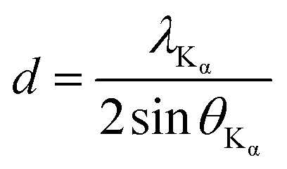 | (1) |
 | (2) |
The remaining peaks were considered to originate from the thin film. These peaks were compared to the powder XRD diffraction patterns in the crystal database (JCPDS) for Miller indexing. For example, the analysis results for the LiCoO2 thin film are shown in Fig. 4. The peaks were identified as the 003n (1 ≤ n ≤ 5) reflections of LiCoO2 by automatic analysis, which is consistent with the results obtained by manual analysis.
 | ||
| Fig. 4 An example of peak identification using the automatic analysis program. The reference data (JCPDS no. 44-0145) were used for comparison. The peaks in the smoothed diffraction pattern (black line) were analyzed, excluding the substrate-origin peaks (marked with a cross) and Kβ radiation peaks (squares). The remaining peaks were compared with the reference data for Miller indexing. The film was deposited using RF magnetron sputtering with a Li1.2CoOx target at an output of 80 W. The substrate temperature was set at 700 °C, with an Ar pressure (P(Ar)) of 0.9 Pa and an O2 pressure (P(O2)) of 0.1 Pa. | ||
3 Results and discussion: autonomous experiments using Bayesian optimization
In dLab, we conducted autonomous experiments using Bayesian optimization. LiCoO2 (001) thin films were deposited on Al2O3 (0001) substrates using RF magnetron sputtering, followed by automatic SEM imaging and XRD measurements. α-LiCoO2 has a layered structure with ordered cations,23,24 and the substrate temperature is a critical parameter determining the degree of ordering.25,26 The higher ordering of cations (Li and Co ions) facilitates two-dimensional Li-ion diffusion, enhancing the battery charge–discharge performance.15,27,28 As an indicator of ordering, we focused on the intensity ratio of the LiCoO2 003 and 006 reflections (I003/I006). A higher peak intensity ratio indicates a higher degree of ordering.29–31 The dLab system automatically analyzed the XRD patterns and calculated the intensity ratio. Using Bayesian optimization, dLab autonomously conducted experiments to maximize the I003/I006 ratio, with the substrate temperature (Ts) as the parameter.The synthesis conditions are listed in Table 1. The SEM image of the sample is shown in Fig. 5(a). A step-and-terrace structure is observed, confirming that the thin film is flat. The measured out-of-plane XRD pattern is shown in Fig. 5(b). A LiCoO2 thin film oriented in the [001] direction has formed on the Al2O3 (0001) substrate, consistent with the earlier reports.23,32
| Target | Li1.2CoOx |
| Substrate | Al2O3 (0001) |
| Total gas pressure | 0.20 Pa |
| Ar partial pressure | 0.18 Pa |
| Oxygen partial pressure | 0.02 Pa |
| RF power | 100 W |
| Substrate temperature (Ts) | 200–750 °C |
| Deposition time | 1 hour |
 | ||
Fig. 5 (a) Scanning electron microscopy image of the LiCoO2 thin film. This image was taken at an accelerating voltage of 10.0 kV and a magnification of 10![[thin space (1/6-em)]](https://www.rsc.org/images/entities/char_2009.gif) 000. It is possible to observe at a magnification of up to 100000. The striped patterns observed in the SEM image are caused by surface structures on the LiCoO2 surface. (b) Raw data of the out-of-plane X-ray diffraction pattern of the LiCoO2 thin film. 000. It is possible to observe at a magnification of up to 100000. The striped patterns observed in the SEM image are caused by surface structures on the LiCoO2 surface. (b) Raw data of the out-of-plane X-ray diffraction pattern of the LiCoO2 thin film. | ||
The films were deposited at various Ts, ranging from 250 to 750 °C. For each sample, the out-of-plane XRD pattern was measured, and the peaks were identified using the aforementioned automatic analysis method to calculate the I003/I006 ratio. When 003 or 006 peaks were not detected, the I003/I006 ratio was set to 0.
The conditions for the Bayesian optimization are listed in Table 2. The Ts, used as the explanatory variable, was selected at 10 °C intervals (56 values in total). Initially, two samples were prepared under the conditions of the lower limit (200 °C) and upper limit (750 °C) of Ts, and the calculated I003/I006 ratio values were registered in the dataset. Next, new synthesis points were proposed using Bayesian optimization (Fig. 6, red line), and deposition and XRD measurements were automatically performed. The closed-loop cycle was performed 25 times (resulting in a total of 27 data points). This process is shown in Fig. 6, and the information for each data point is provided in Table S1.†
| Regression method | Gaussian process regression |
| Kernel function | RBF kernel (variance = 3, length scale = 1.51) |
| Acquisition function (hyperparameter) | UCB (κ = 2.5) |
| Objective variable | I 003/I006 |
| Optimization direction | Maximize |
| Explanatory variable | Substrate temperature (Ts) |
| Total grids | 56 (200, 210, 220, …, 750 °C) |
| Initial data points | 2 (200 °C, 750 °C) |
 | ||
| Fig. 6 Autonomous search process by Bayesian optimization. (a) Initially, deposition was performed at the minimum (250 °C) and maximum (750 °C) substrate temperatures (Ts) within the search range, starting the exploration with two initial data points (two red circles). The red circles represent the ratio of the experimentally obtained X-ray diffraction intensities (I003/I006) for the LiCoO2 003 and 006 peaks on the fabricated thin film samples. The black line represents the prediction curve, and the green area indicates the credible interval. The search point at which the acquisition function is maximum (red line in the figure) is autonomously selected as the next synthesis condition. (b) Red circles represent intermediate results after the 11th experiment. White circles indicate the initial experimental results as shown in (a). (c) Final results after 27 experiments (red circles). White circles represent the previous experimental results as shown in (a) and (b). The highest value of I003/I006 was achieved in the 14th experiment. | ||
Fig. 6 shows the progression of Bayesian optimization. After conducting 25 explorations using Bayesian optimization, the prediction curve indicated that the I003/I006 ratio increases in the Ts range of 600–700 °C. This result indicates that the degree of layered ordering in the LiCoO2 thin films is higher in this temperature range. The maximum I003/I006 ratio (=26.956) was obtained during the 14th exploration (Ts = 660 °C), i.e., the LiCoO2 thin film with the highest crystallinity was achieved at Ts = 660 °C (Table S1†).
Based on the above, we demonstrated autonomous experiments by selecting the Ts as the explanatory variable and the XRD intensity ratio as the objective variable. The diffraction pattern files in MaiML format were automatically analyzed, and Bayesian optimization autonomously proposed and executed the next experimental conditions.
4 Outlook
dLab is expected to evolve as follows.4.1 System expansion to conduct many types of experiments
We envision expanding our dLab system by adding new modular instruments for material synthesis and property evaluation in a plug-and-play manner, thereby extending its functionality. We aim to broaden the scope of material synthesis and develop an autonomous materials exploration system for ceramics, polymers, organic materials, and more. We have confirmed that the robots can also transport and measure circular pellet samples with a diameter of 10 mm and a thickness of 0.5–3 mm (ESI 3†). Therefore, dLab is capable of expanding to other materials and is expected to become a platform for material development.4.2 Recording of material synthesis processes
In dLab, various numerical parameters in the synthesis process, such as substrate temperature, deposition gas flow rate, and pressure, are collected as log data. Combining process data with property measurement data allows us to gain insights into the relationship between synthesis processes and properties. In particular, when unexpected results are obtained in property measurements, associating them with the synthesis process data can contribute to the development of a new knowledge framework. The efficient utilization of the synthesis process data is crucial for future research. The MaiML format enables the entire synthesis process to be structured, which serves as a synthesis instruction manual.4.3 Promotion of sharing instruments and data
We plan to widely share the dLab system and data, both within and outside the academic community. External users will connect to dLab via the internet and perform automated and autonomous synthesis experiments and property evaluations. These approaches would democratize materials science.4.4 Challenges in the dLab system
Here, we address the challenges in terms of cost and complexity. For the former, it is still high to construct the automatic and autonomous system because each module is not standardized. When the inter-instrument communication and physical connections are standardized, a plug-and-play environment is realized. Adopting proposed standards, such as MaiML and Laboratory and Analytical Device Standard (LADS33.) would lead to the plug-and-play environment. Then, the cost would become low. In addition, sharing the system may solve the problem of cost.To tackle the complexity of the system, user-friendly orchestration and scheduling software is the key. Orchestration software works with devices and machine learning algorithms to enable autonomous experimentation.34 The scheduling software manages multiple experimental tasks for multiple samples to proceed with the experiments efficiently. At present, the effort required to create the software is very large. The adoption of microservice and layered architectures that enable flexibility, adaptability, and scalability would establish a plug-and-play environment for software.
5 Summary
We have developed dLab for autonomously synthesizing thin-film samples and measuring their material properties. We demonstrate a system that integrates the experimental modular instruments. By adopting the MaiML format, dLab can utilize any measurement data, independent of the manufacturers. Moving forward, we aim to leverage dLab to accelerate material development.Data availability
The datasets supporting this article have been uploaded as part of the ESI† and are available at our Github repository (https://github.com/Hitosugi24/dLab). The standardization of dLab can be found at https://solid-state-chemistry.jp/ai_robotics/en/standardization.html. The communication protocol is available from https://solid-state-chemistry.jp/ai_robotics/assets/drawing/module_specification_eng.pdf.Author contributions
Conceptualization: Taro Hitosugi; data curation: Kazunori Nishio, Akira Aiba, and Kei Takihara; funding acquisition: Taro Hitosugi; methodology: Kazunori Nishio, Ryota Shimizu, and Taro Hitosugi; project administration: Kazunori Nishio and Taro Hitosugi; resources: Yota Suzuki, Akira Abe, Haruki Baba, Shinichi Katagiri, Kazuki Omoto, and Kazuki Ito; software: Akira Aiba, Kei Takihara, Kazunori Nishio, Ryo Nakayama, and Ryota Shimizu; supervision: Taro Hitosugi; visualization: Kazunori Nishio, Akira Aiba, Kei Takihara and Yota Suzuki; writing – original draft: Kazunori Nishio and Akira Aiba; writing – review & editing: Kei Takihara, Ryo Nakayama, Shigeru Kobayashi, Shinichi Katagiri, Kazuki Ito, Ryota Shimizu and Taro Hitosugi.Conflicts of interest
There are no conflicts to declare.Acknowledgements
This research was supported by the Japan Science and Technology Agency (JST) through the Future Society Creation Project (MIRAI) [JPMJMI21G2], the Strategic Innovation Program (CREST) [JPMJCR22O4], the Japan Society for the Promotion of Science (JSPS) [24K01599], Institute of Science Tokyo Research Infrastructure Management Center Core Facility Center, the Ministry of Education, Culture, Sports, Science and Technology (MEXT) Data-driven Materials Research and Development Project at the University of Tokyo “Center for Research and Development of Electrochemical Materials toward Maximum Introduction of Renewable Energy” (DX-GEM) [JPMXP1122712807], and MEXT Grant-in-Aid for Transformative Research Areas “ion jamology” [24H02203]. We would like to express our sincere gratitude to Professor Kanta Ono at Osaka University for his support in the development of dLab.References
- M. Jansen, Angew Chem. Int. Ed. Engl., 2002, 41, 3746–3766 CrossRef CAS PubMed.
- B. Jandelet, D. J Schaefer, T. S. Powers, H. W. Turner and W. H. Weinberg, Angew Chem. Int. Ed. Engl., 1999, 38, 2494–2532 CrossRef.
- P. G. Schultz and X.-D. Xiang, Curr. Opin. Solid State Mater. Sci., 1998, 3, 153–158 CrossRef CAS.
- N. Ishizuki, R. Shimizu and T. Hitosugi, Sci. Technol. Adv. Mater.: Methods, 2023, 3, 2197519 Search PubMed.
- M. Abolhasani and E. Kumacheva, Nat. Synth., 2023, 2, 483–492 CrossRef CAS.
- E. National Academies of Sciences and Medicine, Automated Research Workflows for Accelerated Discovery: Closing the Knowledge Discovery Loop, 2022 Search PubMed.
- G. Tom, S. P. Schmid, S. G. Baird, Y. Cao, K. Darvish, H. Hao, S. Lo, S. Pablo-Garcia, E. M. Rajaonson, M. Skreta, N. Yoshikawa, S. Corapi, G. D. Akkoc, F. Strieth-Kalthoff, M. Seifrid and A. Aspuru-Guzik, Chem. Rev., 2024, 124, 9633–9732 CrossRef CAS PubMed.
- B. Burger, P. M. Maffettone, V. V. Gusev, C. M. Aitchison, Y. Bai, X. Wang, X. Li, B. M. Alston, B. Li, R. Clowes, N. Rankin, B. Harris, R. S. Sprick and A. I. Cooper, Nature, 2020, 583, 237–241 CrossRef CAS PubMed.
- J. Chen, S. R. Cross, L. J. Miara, J.-J. Cho, Y. Wang and W. Sun, Nat. Synth., 2024, 3, 606–614 CrossRef CAS.
- N. J. Szymanski, B. Rendy, Y. Fei, R. E. Kumar, T. He, D. Milsted, M. J. McDermott, M. Gallant, E. D. Cubuk, A. Merchant, H. Kim, A. Jain, C. J. Bartel, K. Persson, Y. Zeng and G. Ceder, Nature, 2023, 624, 86–91 CrossRef CAS PubMed.
- B. P. Macleod, F. G. L. Parlene, T. D. Morrissey, F. Häse, L. M. Roch, K. E. Dettelbach, R. Moreira, L. P. E. Yunker, M. B. Rooney, J. R. Deeth, V. Lai, G. J. Ng, H. Situ, R. H. Zhang, M. S. Elliot, T. H. Haley, D. J. Dvorak, A. Aspuru-Guzik, J. E. Hein and C. P. Berlingguette, Sci. Adv., 2020, 6, eaaz8867 CrossRef CAS PubMed.
- S. Ichimura, T. Shigefuji, T. Yasunaga and S. Inoue, Oyo Buturi, 2023, 92, 142–146 Search PubMed.
- MaiML format support guidelines are available on https://www.maiml.org/, accessed May 30, 2024.
- K. Mizushima, P. C. Jones, P. J. Wiseman and J. B. Goodenough, Solid State Ionics, 1981, 3–4, 171–174 CrossRef CAS.
- H. J. Orman and P. J. Wiseman, Acta Crystallogr., Sect. C: Cryst. Struct. Commun., 1984, 40, 12–14 CrossRef.
- https://github.com/Hitosugi24/dLab .
- R. Shimizu, S. Kobayashi, Y. Watanabe, Y. Ando and T. Hitosugi, APL Mater., 2020, 8, 111110 CrossRef CAS.
- D. Gall, C.-S. Shin, R. T. Haasch, I. Petrov and J. E. Greene, J. Appl. Phys., 2002, 91, 5882–5886 CrossRef CAS.
- H. Xu, R. Nakayama, T. Kimura, R. Shimizu, Y. Ando, S. Kobayashi, N. Yasuo, M. Sekijima and T. Hitosugi, Sci. Technol. Adv. Mater.: Methods, 2023, 3, 2210251 Search PubMed.
- R. Nakayama, R. Shimizu, T. Haga, T. Kimura, Y. Ando, S. Kobayashi, N. Yasuo, M. Sekijima and T. Hitosugi, Sci. Technol. Adv. Mater.: Methods, 2022, 2, 119–128 Search PubMed.
- X. Ning, I. W. Selesnick and L. Duval, Chemom. Intell. Lab. Syst., 2014, 139, 156–167 CrossRef CAS.
- P. Virtanen, R. Gommers, T. E. Oliphant, M. Haberland, T. Reddy, D. Cournapeau, E. Burovski, P. Peterson, W. Weckesser and J. Bright, Nat. Methods, 2020, 17, 261–272 CrossRef CAS PubMed.
- R. Huang, T. Hitosugi, C. A. Fisher, Y. H. Ikuhara, H. Moriwake, H. Oki and Y. Ikuhara, Mater. Chem. Phys., 2012, 133, 1101–1107 CrossRef CAS.
- M. Antaya, K. Cearns, J. Preston, J. Reimers and J. Dahn, J. Appl. Phys., 1994, 76, 2799–2806 CrossRef CAS.
- M. Antaya, K. Cearns, J. S. Preston, J. N. Reimers and J. R. Dahn, J. Appl. Phys., 1994, 76, 2799–2806 CrossRef CAS.
- R. Huang, T. Hitosugi, C. A. J. Fisher, Y. H. Ikuhara, H. Moriwake, H. Oki and Y. Ikuhara, Mater. Chem. Phys., 2012, 133, 1101–1107 CrossRef CAS.
- K. Mizushima, P. Jones, P. Wiseman and J. B. Goodenough, Mater. Res. Bull., 1980, 15, 783–789 CrossRef CAS.
- T. Hewston and B. Chamberland, J. Phys. Chem. Solids, 1987, 48, 97–108 CrossRef CAS.
- K. Sakamoto, M. Hirayama, H. Konishi, N. Sonoyama, N. Dupré, D. Guyomard, K. Tamura and R. Kanno, Phys. Chem. Chem. Phys., 2010, 12, 3815–3823 RSC.
- K. Nishio, K. Horiba, N. Nakamura, M. Kitamura, H. Kumigashira, R. Shimizu and T. Hitosugi, J. Power Sources, 2019, 416, 56–61 CrossRef CAS.
- K. Nishio, N. Nakamura, K. Horiba, M. Kitamura, H. Kumigashira, R. Shimizu and T. Hitosugi, Appl. Phys. Lett., 2020, 116, 053901 CrossRef CAS.
- T. Tsuruhama, T. Hitosugi, H. Oki, Y. Hirose and T. Hasegawa, Appl. Phys. Express, 2009, 2, 085502 CrossRef.
- https://opcfoundation.org/markets-collaboration/lads/ .
- R. Tamura, K. Tsuda and S. Matsuda, STAM-M, 2023, 3, 2232297 Search PubMed.
Footnote |
| † Electronic supplementary information (ESI) available. See DOI: https://doi.org/10.1039/d4dd00326h |
| This journal is © The Royal Society of Chemistry 2025 |