
 Open Access Article
 This Open Access Article is licensed under a
 Creative Commons Attribution 3.0 Unported Licence
Integrative plasmonics: optical multi-effects and acousto-electric-thermal fusion for biosensing, energy conversion, and photonic circuits†
Hong Zhou‡
 abcd,
Dongxiao Li‡
ab,
Qiaoya Lv‡
ab and
Chengkuo Lee
*abc
abcd,
Dongxiao Li‡
ab,
Qiaoya Lv‡
ab and
Chengkuo Lee
*abc
aDepartment of Electrical and Computer Engineering, National University of Singapore, Singapore 117583, Singapore. E-mail: elelc@nus.edu.sg
bCenter for Intelligent Sensors and MEMS (CISM), National University of Singapore, Singapore 117583, Singapore
cNUS Graduate School-Integrative Sciences and Engineering Programme (ISEP), National University of Singapore, Singapore 119077, Singapore
dSchool of Mechanical Engineering, Northwestern Polytechnical University, Xi’an 710072, China
First published on 12th May 2025
Abstract
Surface plasmons, a unique optical phenomenon arising at the interface between metals and dielectrics, have garnered significant interest across fields such as biochemistry, materials science, energy, optics, and nanotechnology. Recently, plasmonics is evolving from a focus on “classical plasmonics,” which emphasizes fundamental effects and applications, to “integrative plasmonics,” which explores the integration of plasmonics with multidisciplinary technologies. This review explores this evolution, summarizing key developments in this technological shift and offering a timely discussion on the fusion mechanisms, strategies, and applications. First, we examine the integration mechanisms of plasmons within the realm of optics, detailing how fundamental plasmonic effects give rise to optical multi-effects, such as plasmon–phonon coupling, nonlinear optical effects, electromagnetically induced transparency, chirality, nanocavity resonance, and waveguides. Next, we highlight strategies for integrating plasmons with technologies beyond optics, analyzing the processes and benefits of combining plasmonics with acoustics, electronics, and thermonics, including comprehensive plasmonic-electric-acousto-thermal integration. We then review cutting-edge applications in biochemistry (molecular diagnostics), energy (harvesting and catalysis), and informatics (photonic integrated circuits). These applications involve surface-enhanced Raman scattering (SERS), surface-enhanced infrared absorption (SEIRA), surface-enhanced fluorescence (SEF), chirality, nanotweezers, photoacoustic imaging, perovskite solar cells, photocatalysis, photothermal therapy, and triboelectric nanogenerators (TENGs). Finally, we conclude with a forward-looking perspective on the challenges and future of integrative plasmonics, considering advances in mechanisms (quantum effects, spintronics, and topology), materials (Dirac semimetals and hydrogels), technologies (machine learning, edge computing, in-sensor computing, and neuroengineering), and emerging applications (5G, 6G, virtual reality, and point-of-care testing).
 Hong Zhou | Hong Zhou received his BEng degree in Mechanical Engineering from Central South University, China, and his PhD degree in Instrument Science and Technology from Chongqing University, China, in 2020. From 2021 to 2025, he was a Research Fellow with the Department of Electrical and Computer Engineering at the National University of Singapore. He is currently a Professor at the School of Mechanical Engineering, Northwestern Polytechnical University, China. His research interests include plasmonics, mid-infrared metamaterials and nanophotonics for advanced sensing applications. |
 Dongxiao Li | Dongxiao Li received his BSc degree from the College of Artificial Intelligence, Chongqing Technology and Business University, Chongqing, China, and PhD degree in Instrument Science and Technology from Chongqing University, China, in 2022. He is now a Research Fellow at the Department of Electrical & Computer Engineering, National University of Singapore, Singapore. His research interests are focused on mid-infrared metamaterials and nanophotonics for sensing applications. |
 Qiaoya Lv | Qiaoya Lv is currently engaged in pursuing her PhD in Instrumentation Science and Technology at Chongqing University. Her research is centered around the design and fabrication of piezoelectric MEMS sensors, actuators, and energy harvesters. In addition, she is actively involved in the DFT calculations concerning the plasmonic nanostructures, and photocatalytic, piezoelectric, and elastic properties of materials. |
 Chengkuo Lee | Chengkuo Lee received his PhD degree in Precision Engineering from the University of Tokyo in 1996. Currently, he is the director of the Center for Intelligent Sensors and MEMS at the National University of Singapore, Singapore. In 2001, he cofounded Asia Pacific Microsystems, Inc., where he was the Vice President. From 2006 to 2009, he was a Senior Member of the Technical Staff at the Institute of Microelectronics, A-STAR Singapore. He has contributed to more than 516 peer-reviewed international journal articles. |
1. Introduction
Surface plasmons are the collective oscillations of free electrons that occur at the interface between a metal (typically gold or silver) and a dielectric material upon optical excitation. To describe the coupled oscillations of electromagnetic waves and charge carriers in solids, surface plasmons are often referred to as surface plasmon polaritons (SPPs) by adding the word “polaritons”. The study of surface plasmons dates back to the early 20th century, with significant milestones marking its development. The first experimental observation of plasmonic enhancement was reported by Wood in 1902,1 who noted an anomalous decrease in light intensity reflected by a metallic grating. Over time, theoretical work and key experimental breakthroughs2—such as the discovery of surface-enhanced Raman scattering (SERS),3 surface-enhanced infrared absorption (SEIRA),4 and surface-enhanced fluorescence (SEF)5—established a foundation for numerous applications in sensing,6 imaging,7 spectroscopy, photonic devices,8 and solar energy harvesting.9–12 Surface plasmons continue to be a vibrant area of research, with ongoing discoveries expanding their potential applications and deepening our understanding of plasmonic phenomena.Currently, the study of plasmons is evolving from “classical plasmonics” to “integrative plasmonics”—a transition that shifts focus from understanding only the fundamental phenomena to exploring the rich interplay of optical multi-effects combined with electric, acoustic, and thermal technologies (Fig. 1). Classical plasmonics has provided deep insight into the properties of surface plasmons and their interactions with light; yet it faces significant challenges such as ohmic losses in metals and inherent scalability issues. These losses lead to significant energy attenuation, and while classical designs are compact, they often dissipate too much energy to be effective over practical distances. Integrative plasmonics overcomes these limitations by adopting innovative strategies. For example, by employing hybrid photonic-plasmonic structures,13 light can travel long distances within low-loss photonic waveguides, converting to plasmons only in small, localized regions for specific tasks such as processing or sensing.
 | ||
| Fig. 1 Roadmap of integrative plasmonics. Since the discovery of plasmons in 1902, a diverse range of plasmonic effects have been observed, such as SPR, LSPR, SERS, and SEIRA. Currently, the study of plasmons has evolved from focusing on the basic plasmon effect to exploring optical multi-effects and the fusion with electric, acoustic, and thermal technologies, which is referred to as “integrative plasmonics”. These advancements are demonstrated in cutting-edge applications across molecular diagnostics, energy conversion, and photonic integrated circuits. | ||
Furthermore, while classical plasmonic experiments typically address a single function—like using nanoparticles to sense local refractive index changes—integrative plasmonics allows multiple plasmonic elements to operate in concert. This facilitates the creation of complex, multifunctional devices, such as an integrated plasmonic circuit containing sources, modulators, waveguides, and detectors all on one chip. Such complexity is vital for advancing plasmonics from laboratory demonstrations to practical, high-performance devices. For instance, the combination of plasmonic near-field enhancement with the graphene bulk photovoltaic effect (BPVE) has already demonstrated zero-bias photodetection capabilities.14 Similarly, the integration of local plasmonic heating with the photoacoustic (PA) effect enables simultaneous ultrasound imaging and imaging-guided thermal treatment of tumors, paving the way for more precise diagnostic and therapeutic solutions.15
Thus, we refer to this emerging interdisciplinary field as “integrative plasmonics”, emphasizing the fusion of optical multi-effects with acousto-electrical-thermal phenomena. This integrated approach not only overcomes traditional limitations but also offers innovative methods and technological solutions for specific challenges in applications such as biosensing, energy conversion, and photonic circuits. As technological advancements continue and interdisciplinary collaborations deepen, the scope of plasmonic effects is set to expand further, spurring breakthrough innovations. Consequently, a systematic and comprehensive discussion of optical multi-effects and acousto-optical-thermal integration is crucial to propel the field forward. Key areas of focus include (1) the advantages of integrative plasmonics; (2) strategies for enhancing the optical multi-effects of plasmons; (3) approaches for fusing acousto-electric-thermal technologies; (4) emerging mechanisms and applications; and (5) the future development of integrative plasmonics.
In this review, we aim to address these questions by providing a comprehensive analysis of the optical multi-effects of plasmons and the fusion of plasmonic, acoustic, electric, and thermal technologies. Our objective is to offer a timely discussion and perspectives on the mechanisms, strategies, and applications of integrative plasmonics. The framework of this review is illustrated in Fig. 2. Firstly, we introduce and analyze the optical multi-effects of plasmons. This section covers various phenomena, including plasmon–phonon coupling, plasmonic nonlinear optical effects, electromagnetically induced transparency (EIT), plasmonic chirality, plasmonic nanocavity resonance, and plasmonic waveguide resonance. Through this analysis, we elucidate how basic plasmonic effects evolve into complex optical multi-effects, representing the integration of multiple effects within the realm of optics. Secondly, we analyze the multiphysical coupling of plasmons with acoustics, electronics, and thermal effects, emphasizing their comprehensive integration. This analysis highlights the strategies for combining plasmonic effects with technologies beyond optics, providing insights into how these integrations are achieved and their potential benefits. In the subsequent sections, we examine the cutting-edge and promising applications of integrative plasmonics. These applications include molecular diagnostics, energy conversion, and photonic integrated circuits (PICs). This section demonstrates the advantages of integrative plasmonics in addressing complex real-world challenges, showcasing its potential to drive innovations across various fields. Finally, we conclude with a forward-looking perspective on the future of integrative plasmonics. We offer personal views on the challenges and the potential developments in the field, emphasizing the importance of continued research and interdisciplinary collaboration for mechanism advancements, material innovations, technological breakthroughs, and application expansion, to unlock the full potential of integrative plasmonics. By following this framework, our review aims to provide a thorough understanding of the current state and future prospects of integrative plasmonics, contributing to the advancement of this rapidly evolving field.
 | ||
| Fig. 2 Framework of this review. First, the optical multi-effects in integrative plasmonics are highlighted, followed by a discussion of the fusion of plasmons with electric, acoustic, and thermal technologies. We then review cutting-edge applications of these technologies in molecular diagnostics, energy conversion, and photonic integrated circuits. Finally, we conclude with a forward-looking perspective on the future of integrative plasmonics. | ||
2. Mechanics of optical multi-effects
To understand why optical multi-effects and electric-acousto-thermal fusion are pivotal features of integrative plasmonics, we first examine the excitation mechanism of plasmons, as illustrated in Fig. 3. When metal nanoparticles or nanorods interact with light, the conduction electrons in the metal are driven by the incident electric field into collective oscillations, namely localized surface plasmon polaritons (LSPPs).16–28 The energy of the plasmon can decay both non-radiatively, resulting in absorption, and radiatively, resulting in light scattering (Fig. 3a). The non-radiative decay of the plasmon involves relaxation through electron–electron collisions or electron-lattice phonon coupling, generating hot electrons—a crucial step in the process. Hot electrons, which are not in thermal equilibrium with the atoms in the material,29 are characterized by an elevated effective temperature described by the Fermi function.30 They are generated via intraband excitations within the conduction band or through interband excitations involving transitions between other bands (e.g., d bands) and the conduction band (Fig. 3b). Notably, interband excitations are less probable than intraband excitations due to the lower energy levels of the d bands.31 The generation of hot electrons is accompanied by heating effects and thermal expansion phenomena (Fig. 3c). Specifically, after the initial electronic excitation, relaxation occurs on a sub-picosecond timescale via electron–electron scattering, leading to localized heating and a rapid increase in the metal surface temperature. This creates a significant temperature difference between the hot nanostructure surface and the cooler surrounding medium, resulting in heat exchange. During this process, thermal expansion and contraction of the surrounding medium generate ultrasonic signals. In this context, hot electrons correspond to electronic effects, heating effects correspond to thermionic effects, and thermal expansion generates ultrasound, corresponding to acoustic effects. Therefore, optical-electric-acousto-thermal fusion is a key feature of integrative plasmonics (Fig. 3d). | ||
| Fig. 3 Mechanics and categories of integrative plasmonics. (a) Schematic diagram of plasmonic nanoparticles and nanorods, with energy loss occurring via radiative and non-radiative decay. (b) Non-radiative decay involves the excitation of hot electrons. These hot electrons are generated through intraband excitations within the conduction band or interband excitations from transitions between other bands (e.g., d bands) and the conduction band. (c) The excitation of hot electrons is accompanied by heating effects and thermal expansion phenomena. (d) Hot electrons correspond to electronics, heating effects correspond to thermonics, and thermal expansion can generate ultrasound, which corresponds to acoustics. Therefore, optical-electrical-acousto-thermal fusion is an important feature of integrative plasmonics. (e) Radiative decay of plasmons leads to near-field and far-field enhancements, producing different plasmonic effects with various materials across the terahertz to ultraviolet regions. (f) These plasmonic effects combine with other optical mechanisms to create optical multi-effects, such as plasmon–phonon coupling, which is another important feature of integrative plasmonics. Optical multi-effects have been shown to enable new functionalities and improve device performance in the optical field. | ||
Regarding radiative decay, LSPPs generate strong electromagnetic fields at the surfaces of nanostructures, with local field strengths that can be several orders of magnitude greater than the incident field.32–34 This enhancement spans various plasmonic effects from the terahertz to the UV regions (Fig. 3c). For example, in the visible light spectrum, plasmon-driven phenomena such as SERS,35 SEF,36 and surface plasmon resonance37 have been experimentally observed. In the infrared region, due to molecular infrared vibration modes, the plasmon-driven SEIRA effect is widely utilized in molecular detection and imaging.38,39 Recently, these plasmonic effects have been shown to combine with other optical mechanisms to create optical multi-effects,40 enabling new functionalities or improving device performance. For instance, plasmon–phonon coupling has been demonstrated to achieve light–matter coupling in the ultrastrong coupling (USC) regime,41 which holds promise for the development of novel ultrafast devices.42 In the following sections, we will explore six optical multi-effects in detail, illustrating strategies for integrating plasmons with other effects in the field of optics. These multi-effects include plasmon–phonon coupling, plasmon-enhanced electromagnetically induced transparency/absorption, plasmonic nanocavity resonance, plasmon-enhanced nonlinear optical effects, plasmon-enhanced chirality, and plasmonic waveguide resonance.
2.1 Plasmon–phonon coupling
Surface phonon polaritons (SPhPs) arise from the interaction between polar optical phonons and long-wavelength incident fields, spanning from the mid-IR range (e.g., hexagonal BN43) to frequencies below 10 THz (e.g., GaAs44). These interactions occur in polar dielectric crystals between the longitudinal (LO) and transverse optic (TO) phonon frequencies, within a spectral range known as the “Reststrahlen” band.45 Due to their excitation in polar dielectric crystals, SPhPs exhibit excellent optical properties, including lower optical losses compared to plasmonic materials, high local electromagnetic fields, and large Purcell factors. Plasmons can harness these superior optical properties by coupling with phonons.41Plasmon–phonon coupling emerges when the collective oscillations of free electrons in metals or semiconductors interact with phonon modes in polar crystals. While plasmons typically reside in the visible to near-infrared range, phonon polaritons occur in the mid-infrared to terahertz regime (the Reststrahlen band). The overlap in these spectral domains enables hybrid modes that can combine the best attributes of both plasmons and phonons, leading to promising opportunities for enhanced light–matter interactions. The advantages of the hybrid modes include the following: (1) lower optical losses: polar dielectrics like h-BN (hexagonal boron nitride) exhibit lower losses in the mid-IR or terahertz regime compared to many metals at similar frequencies. Coupling plasmons to SPhPs can reduce the overall dissipation; (2) high local field enhancement: just as plasmons localize electromagnetic fields at subwavelength scales, SPhPs also confine light strongly. Their combination may further enhance this confinement, beneficial for sensing and nonlinear optical processes; and (3) tunable response: by engineering the dimensions of nanostructures or by choosing specific polar dielectrics, it becomes possible to tailor the plasmon–phonon resonant frequency, quality factor, and spatial confinement.
Plasmon–phonon coupling can be theoretically analyzed using an oscillator model consisting of three coupled harmonic oscillators subjected to an external force f, as illustrated in Fig. 4a. The two damped oscillators represent out-of-phase atomic lattice vibrations, with k-vectors aligned parallel (LO) and perpendicular (TO) to the incident field. According to the coupled harmonic oscillator theory, the coupling system can be expressed as follows:46
 | (1) |
 | (2) |
 | (3) |
![[thin space (1/6-em)]](https://www.rsc.org/images/entities/char_2009.gif) exp(iφ), where φ represents the phase shift between them. γL denotes the bright-mode damping factor. Based on this relationship, the spectra of the plasmon–phonon coupling system can be obtained, as illustrated in Fig. 4b. In a coupled system, phonons remain fixed in the Reststrahlen band, while the plasmon resonance bifurcates into two distinct frequencies, known as the upper and lower branch frequencies. The phonon intensity varies with the coupling coefficient κ. This splitting behavior is more apparent in the dispersion curves of the plasmon–phonon coupling system (Fig. 4c). Different positions on the split correspond to varying plasmonic resonance frequencies. Since the SPhP Reststrahlen band remains fixed, altering the plasmonic resonance frequency Δω results in different coupling strengths, which in turn affect the SPhP vibration intensity. For example, when the plasmonic resonance frequency shifts from ωA to ωB, the split moves from A to B. This redshift-induced intensity change of SPhPs can enhance identification accuracy in molecular diagnostic applications. The redshift can be caused by perturbations in the refractive index.
exp(iφ), where φ represents the phase shift between them. γL denotes the bright-mode damping factor. Based on this relationship, the spectra of the plasmon–phonon coupling system can be obtained, as illustrated in Fig. 4b. In a coupled system, phonons remain fixed in the Reststrahlen band, while the plasmon resonance bifurcates into two distinct frequencies, known as the upper and lower branch frequencies. The phonon intensity varies with the coupling coefficient κ. This splitting behavior is more apparent in the dispersion curves of the plasmon–phonon coupling system (Fig. 4c). Different positions on the split correspond to varying plasmonic resonance frequencies. Since the SPhP Reststrahlen band remains fixed, altering the plasmonic resonance frequency Δω results in different coupling strengths, which in turn affect the SPhP vibration intensity. For example, when the plasmonic resonance frequency shifts from ωA to ωB, the split moves from A to B. This redshift-induced intensity change of SPhPs can enhance identification accuracy in molecular diagnostic applications. The redshift can be caused by perturbations in the refractive index.
 | ||
| Fig. 4 Strategies for plasmon–phonon coupling. (a) Schematic view of two coupled damped oscillators with a driving force f applied to one of them. (b) Spectra of the plasmon–phonon coupling system based on the model in (a). (c) The dispersion curves of the plasmon–phonon coupling system. The curve describes how a refractive index change (from n1 to n2) causes a change in the resonant frequencies of plasmons (ω+,−). It describes the spectral change when the resonant frequencies of plasmons vary due to perturbations in the refractive index. (d) Schematic diagram of plasmon–phonon coupling. The black balls represent plasmons with the collective oscillations of free carriers in metals, and the red and white balls are phonons with atomic displacements in the form of optical phonons in polar dielectrics. (e) An example of phonon–photon coupling for the biosensing of glucose oxidase (GOD). Adapted with permission from ref. 47; Copyright 2023 Springer Nature. (f) An example of polarization-controlled phonon–photon coupling for the hyperspectral imaging application. Adapted with permission from ref. 46; Copyright 2024 Springer Nature. | ||
For instance, our group proposed a strategy to achieve phonon and plasmon coupling, as illustrated in Fig. 4d. This approach utilizes stacked trapezoidal metal (Au) antennas and phonon (silicon oxide, SiO2) antennas, all situated on a BaF2 substrate. The metal antennas support plasmons through the collective oscillations of free carriers, while the SiO2 antennas support phonons through atomic displacements. The coupling of phonons and plasmons has been shown to improve identification accuracy when molecular vibrational fingerprints overlap, which is crucial for molecular diagnostic applications (Fig. 4e).47 In one demonstration monitoring the glucose enzymatic reaction, SPhP vibrations were able to disentangle overlapping vibrational modes of glucose oxidase and water, achieving a 92% identification accuracy.
Furthermore, the coupling of phonons and plasmons can be controlled by the optical response of the nanostructure, such as polarization, ensuring that plasmon and phonon signals can be independently manipulated. This prevents mutual interference and signal masking.46 As shown in Fig. 4f, the asymmetric design of cross-shaped nanoantennas with unequal arm lengths allows for strategic control. The plasmonic resonance frequency of the short arms is positioned away from the phonon frequency but aligns with the vibrational frequency of protein samples for vibrational imaging. Conversely, the plasmonic resonance frequency of the long arms aligns with the phononic Reststrahlen band to excite phonon modes for imaging. By manipulating the polarization direction, selective excitation of plasmonic modes in the short arms or phonon modes in the long arms is achieved. This system demonstrates increased identification accuracy, heightened sensitivity, and enhanced detection limits, down to molecule monolayers, for mid-infrared hyperspectral imaging of severe acute respiratory syndrome coronavirus (SARS-CoV).46
In addition to altering optical properties, plasmon–phonon interactions can influence the electron scattering mechanism and, consequently, the electrical conductivity of the material.48 The interaction between plasmons and phonons can be tuned by adjusting parameters such as doping levels, material composition, and temperature.49 This tunability allows for precise control of electrical properties in devices. Moreover, understanding and controlling plasmon–phonon coupling can lead to improved thermal management in electronic and photonic devices, as well as enhanced performance in thermoelectric materials.50 For example, plasmon–phonon coupling in graphene/hBN systems can be used to flexibly modify the spectral emissivity of a thermal emitter.51 In general, the integration of SPhPs will facilitate plasmon-based applications such as optical sensing, photodetection, and thermal management.
2.2 Electromagnetically induced transparency/absorption
Combining plasmons with quantum-like effects can improve the complexity and functionality of these phenomena. EIT is a quantum interference effect that makes an otherwise opaque medium transparent to a probe laser beam when a control laser beam is applied. EIT typically occurs in a three-level atomic system consisting of two ground states and one excited state but often requires cryogenic temperatures. Electromagnetically induced absorption (EIA), closely related to EIT, results in enhanced absorption rather than transparency.52 In the context of EIT/EIA, surface plasmons can achieve destructive or constructive interference effects analogous to those observed in atomic EIT/EIA, creating transparency or absorption windows. It is useful to note that the phenomena of transmission, reflection, and absorption are inherently connected through the relationship A + T + R = 1; hence, any increase in reflection (sometimes described as electromagnetically induced reflection) or transmission can be interpreted in terms of a corresponding change in the absorption spectrum. Plasmon-driven EIT/EIA offers several advantages, including subwavelength control, versatility, integration, and room temperature operation. For example, plasmonic structures can confine light to subwavelength dimensions, leading to strong field enhancements and enabling EIT/EIA effects at the nanoscale.53 Additionally, unlike some atomic systems that require cryogenic temperatures, plasmonic EIT/EIA can function at room temperature, making them more practical for real-world applications.The plasmon-driven EIT/EIA can be analyzed using a coupled harmonic oscillator model (Fig. 5). According to this model, the spectral response of the plasmon system for the EIT/EIA effects can be described as54
 | (4) |
 | ||
| Fig. 5 Plasmon-driven electromagnetically induced transparency/absorption. (a) Schematic view of electromagnetically induced transparency/absorption (EIT/EIA) of a plasmonic device.54 According to the coupled harmonic oscillator model, when the dark damping γm is coupled to the plasmonic system, its spectral response depends on the coupling strength κ·exp(i·2φ), where the phase (φ) of Fano resonance is critical and has three states: (I) 0 < φ < π/4, EIT state; (II) φ = π/4, critical coupling; and (III) π/4 < φ < π/2, EIA state. (b) Utilizing the reflection of a metal layer close to the plasmonic nanostructure to change the phase φ. (c) The phase φ as a function of distance T to the plasmonic nanostructure. (d) The current distribution of the plasmonic nanostructure (I) without a metal reflection layer, or with a metal reflection layer whose gap varies (II–IV). Adapted with permission from ref. 54; Copyright 2022 John Wiley and Sons. | ||
The plasmon-driven EIT/EIA offers high-quality factors and low radiation losses, which are advantageous for the development of efficient photonic devices. These phenomena also enable steep linear dispersion in transparency windows, leading to an elevated group refractive index. For example, combining graphene with dielectric metasurfaces can achieve actively tunable ring-shaped EIT, where graphene plasmons can be controlled by adjusting the Fermi level through applied voltage.55 EIT-based sensors are particularly sensitive to changes in the dielectric environment due to their high Q factor and strong local electric fields.56 Additionally, by creating a transparency window, the group velocity of light passing through the medium can be significantly slowed down. Plasmon-driven EIT structures thus facilitate the realization of slow light devices in compact, integrated photonic circuits.57
2.3 Plasmonic nanocavity resonance
While individual plasmonic nanoparticles exhibit excellent light manipulation capabilities, nanocavities formed by assemblies of plasmonic particles, such as nanosphere dimers and trimers,58–61 have garnered significant attention. These nanocavities, created by strategically assembling two or more individual nanoparticles, offer much stronger field intensities for enhanced light–matter interactions.62 The narrow gaps between the particles enable more efficient light confinement compared to the individual constituent particles. Moreover, the plasmon coupling between constituent particles can generate a wider variety of intriguing plasmon modes, providing greater flexibility in manipulating the optical properties of the assembled nanostructures. Notable examples include bonding and anti-bonding plasmon modes in metal nanoparticle dimers,63 super-radiant and sub-radiant plasmons in ring/disk nanocavities, and plasmonic Fano resonances in metal nanoparticle oligomers.64–67Next, we introduce the nanofabrication strategies for realizing plasmonic nanocavities, specifically highlighting single nanoparticles on a film and dimers on a film. The size of the nanogap in the nanocavity is crucial as it affects the near-field coupling strength between the nanoparticles and the film.68 There are two primary strategies for precisely controlling the nanogap size during nanofabrication. The first approach involves separating the nanoparticles from the metal film by depositing a planar dielectric film between them, with the nanogap size being adjusted by controlling the thickness of the dielectric film (Fig. 6a). The second method uses a dielectric shell coating around the metal nanoparticles to form core/shell-type nanoparticles, thereby avoiding direct contact between the metal nanoparticles and the underlying film (Fig. 6b). The nanogap size in this method is tuned by adjusting the thickness of the dielectric shell. Several methods can be employed to fabricate nanogaps, each offering distinct characteristics. The layer-by-layer (LBL) method involves depositing alternating monolayers of positively charged poly(allylamine)hydrochloride (PAH) and negatively charged polystyrene sulfonate, allowing precise control over thickness ranging from 2 to 20 nm.69 Atomic layer deposition (ALD) achieves nanoscale-thick inorganic spacers by depositing one molecular layer per cycle, producing materials like Al2O3 and SiO2 with thickness ranging from a few nanometers.70 Self-assembled monolayers (SAMs) of amine-terminated alkanethiols create ultrathin spacers with thicknesses between 0.5 and 2 nm, controlled by the length of the alkanethiol molecules.71 Finally, two-dimensional (2D) materials such as graphene and transition metal dichalcogenides provide natural ultrathin spacers with atomic thickness, scalable to a few nanometers using mechanical exfoliation or chemical vapor deposition.72 These strategies enable precise control over nanogap size, which is essential for optimizing the near-field coupling strength and enhancing the performance of plasmonic nanocavities.
 | ||
| Fig. 6 Strategies for plasmonic nanocavity resonance. (a) Schematic view of a single nanoparticle-on-film construct. (b) Schematic of the core/shell type nanoparticle-on-film strategy. (c) Schematic illustration of plasmonic dipole approximation for nanoparticles-on-film configurations. (d) 3D surface charge distributions of the dimer-on-film. Upper panel: Mirror-induced bonding dipole plasmon (MBDP) mode I. Lower panel: MBDP mode II. (e) Extracted peak intensity of MBDP modes I and II as a function of the dimer gap g. Adapted with permission from ref. 63; Copyright 2016 Springer Nature Limited. | ||
The impact of nanocavity on plasmonic modes can be explored by analyzing the nanogap using various theoretical analytical tools. One such method is based on the multiple scattering process,73 as illustrated in Fig. 6a. For the incident wave Sin, the scattering waves include reflection of the incident wave by the film without the nanoparticle SR, reflection of the scattered wave from the nanoparticle by the metal film SRP, and the scattered wave from the nanoparticle SP. Another approach is the dipole-image model within the electrostatic approximation, as depicted in Fig. 6c. For a nanostructure positioned close to a sufficiently large metal film, the plasmonic properties of the entire system are equivalent to those of a dimer consisting of the real nanostructure and its corresponding image in the metal film.74 Additionally, an equivalent circuit model can be used to describe the nanoparticle-film gap plasmon oscillations, offering another perspective on these interactions.75
Consider the dimer-on-film design as an example; the simulated 3D surface charge distributions are illustrated in Fig. 6d. The results reveal a strong correlation between the surface plasmon geometry and the local electric field distributions. When two nanoparticles are in close proximity, forming a dimer, the localized charge intensities become particularly significant at the nanogap. Additionally, dual dipole modes are observed: one arising from the vertical bonding between the dimer dipole and the induced charge dipoles, and the other from the horizontal bonding. The image poles in the mirror result from the interaction with the neighboring opposite poles of the nanoparticles, where the mirror induces multiple plasmon poles. As depicted in the peak intensity plot (Fig. 6e), as the gap size g increases, the peak intensity decreases almost exponentially due to the rapid degeneration of the nanoparticles’ hot-spots.
2.4 Plasmon-enhanced nonlinear optical effects
Nonlinear optical effects are crucial for modern photonic functionalities,76–78 such as frequency control of laser light,79 ultrashort pulse generation,80 all-optical signal processing,81 and ultrafast switching.82 However, these effects are inherently weak due to the limited photon–photon interactions in materials. Integration of plasmonics with these effects can address this challenge. First, plasmons can significantly enhance these nonlinear optical effects due to the coherent oscillations of conduction electrons near noble-metal surfaces. Surface plasmons generate strong local electromagnetic fields, thereby boosting optical processes like SERS and increasing effective nonlinearities.83–86 For example, in SERS, plasmon excitation of rough or engineered metal surfaces can enhance the inherently weak Raman process by several orders of magnitude, even enabling single-molecule detection.87–90 Additionally, plasmonic excitations are highly sensitive to changes in dielectric properties, enabling precise control of light with light. These excitations also operate on femtosecond timescales, facilitating ultrafast optical signal processing and leading to advanced nanophotonic functionalities. For instance, this picosecond optical modulation could be used to create integrated optical components with terahertz modulation speeds.91Next, three representative strategies for plasmon-enhanced nonlinear optical effects are introduced. The first is the nonlinear second-harmonic generation (SHG).92 The suggested energy level structure and SHG pathway are exhibited in Fig. 7a. This method doubles the frequency of light through the interaction between light and nonlinear materials, which is an essential optical technology. However, due to the long interaction length between light and nonlinear materials, conventional components that achieve this function are often bulky. One solution is to embed plasmonic materials into materials with high intrinsic optical nonlinearity, which can achieve high nonlinear response at moderate powers. For instance, plasmonic gold nanorings were filled with lithium niobate (LN) using electron beam lithography and ion beam enhanced etching (Fig. 7b).93 This configuration has been demonstrated to enhance SHG, with an EF of up to 60 (Fig. 7c). This approach offers a compact and efficient solution, making it highly suitable for practical applications in fluorescence spectroscopy and quantum communication.
 | ||
| Fig. 7 Strategies for plasmon-enhanced nonlinear optical effects. (a) Photon diagrams for second-harmonic generation (SHG). The solid horizontal lines correspond to real quantum mechanical states of the material system, while the dashed lines are virtual states in which the system resides only momentarily. The orange arrows correspond to input fields that can drive the energy of the material system up or down as directed. The blue downward arrows correspond to the generated fields that return the material to its initial state. (b) Plasmon-enhanced SHG in gold nanoring resonators filled with lithium niobate. (c) Measured second-harmonic enhancement factor and linear reflection spectrum of the device in (b). Adapted with permission from ref. 93; Copyright 2015 American Chemical Society. (d) Photon diagrams for four-wave mixing (FWM). (e) Mechanism of the plasmon-enhanced FWM. (f) FWM using a gold azimuthally chirped grating. Adapted with permission from ref. 94; Copyright 2023 John Wiley and Sons. (g) Photon diagrams for surface-enhanced coherent anti-Stokes Raman scattering (SECARS). (h) SECARS configuration of two diluted molecules on a nanoquadrumer. A single-wavelength pump laser (ωP) and a supercontinuum Stokes laser (ωS) generate an enhanced anti-Stokes scattering (ωS) of a molecule in the quadrumer central gap. (i) Corresponding SECARS enhancement map. Adapted with permission from ref. 95; Copyright 2014 Springer Nature. | ||
The second is the four-wave mixing (FWM) effect, which is a parametric nonlinear process in which two optical electromagnetic waves that have two different frequencies interact to form another two optical waves of different frequencies, as shown in Fig. 7d. FWM has widespread applications in wavelength conversion, signal regeneration, switching, phase-sensitive amplification, nonlinear imaging and entangled photon pair generation. However, FWM processes have an extremely weak nature and suffer from very poor efficiencies. The key towards improving the efficiency of FWM is to increase the local field intensity along nonlinear materials. The enhanced electromagnetic fields of plasmonic structures can serve well to boost the nonlinear FWM process. The mechanism of the plasmon-enhanced FWM is shown in Fig. 7e. When two different frequency components (ω1,2) of an electromagnetic wave propagate together on the plasmon surface, a refractive index modulation at the frequency difference between the two occurs and this creates two additional frequency components (ω4wm1 = 2ω1 − ω2, ω4wm2 = 2ω2 − ω1).96 For instance, Chakraborty et al. used a plasmonic azimuthally chirped grating (ACG) to enhance the nonlinear optical process by coupling light from the far field into localized hot spots (Fig. 7f).94 They demonstrated significant enhancement of broadband FWM due to the interplay between localized surface plasmon resonance (LSPR) and plasmonic surface lattice resonance in the ACG.
The third is the surface-enhanced coherent anti-Stokes Raman scattering (SECARS).97 As shown in Fig. 7g, in conventional SERS,98–103 Stokes-Raman scattering (ωS) is generated for the excitation of the pump (ωP). The SERS can be further improved by combining plasmonic enhancements with coherence, that is, the pump (ωP) and Stokes (ωS) fields interact coherently through the high-order polarizability of the dipole-forbidden vibronic modes of a molecule, generating an anti-Stokes signal ωAS = 2ωP − ωS. If the input (ωP,S) or output (ωAS) frequencies are in resonance with the collective modes of the plasmonic nanostructure, the signal from molecules adsorbed onto the nanostructure will be further enhanced by the local fields of the excited plasmon modes, which is known as SECARS. For instance, Zhang et al. developed a quadrumer consisting of four gold nanodisks arranged to create a strong Fano resonance (Fig. 7h), thereby achieving a highly localized SECARS enhancement in a single junction at the center of the quadrumer structure (Fig. 7i).95 The detection signal is enhanced by ∼11 orders of magnitude, enabling the detection of single molecules in the demonstration.
2.5 Plasmon-enhanced chirality
A chiral object or system is defined as one whose structure and mirror image (enantiomer) are not superimposable.104–106 Chiral structures are ubiquitous in nature, exemplified by deoxyribonucleic acid (DNA) and proteins.107,108 While chirality is inherently a qualitative property, chiral optical systems can be quantitatively described using parameters such as optical activity (OA)/optical rotation (OR) and circular dichroism (CD)/circular conversion dichroism (CCD). OA/OR and CD/CCD quantify the rotation of the polarization plane of linearly polarized light and the differential transmittance/reflectance of left-circularly polarized (LCP) versus right-circularly polarized (RCP) light, respectively. Natural materials typically exhibit weak chiral optical properties due to the large mismatch between their atomic feature sizes and optical wavelengths.109,110 Plasmonic systems, however, are promising solutions to this limitation because of their strong light–matter interactions. Consequently, methods to enhance and tailor the chiral optical response in plasmonic systems are highly valued.Plasmonic chirality is usually categorized into intrinsic and extrinsic chirality. Intrinsic chirality arises from the geometry of the nanostructure itself, where the structure lacks any internal symmetry planes that would render it achiral. An intrinsically chiral plasmonic nano-object remains chiral irrespective of how it is illuminated because its handedness is “built into” its three-dimensional (3D) form. This intrinsic handedness cannot be altered by changing external parameters such as the incident angle or polarization of light.111 A classic example is a spring-shaped (helical) metal nanostructure (Fig. 8a). Such a helix has a well-defined right- or left-handed geometry, ensuring a robust chiral response (e.g., CD, OR) under various illumination conditions. In contrast, extrinsic chirality is not an inherent property of the structure but is induced by the specific illumination conditions. For instance, a plasmonic split ring resonator, typically an achiral object, can exhibit a chiral optical response when the incident wave vector does not lie in its symmetry plane (Fig. 8b).112 This phenomenon is especially useful for tunable or reconfigurable plasmonic devices. By simply rotating the sample or changing the polarization and angle of the incident beam, devices can dynamically respond to external stimuli (e.g., changes in the environment, polarization switching), making them suitable for sensing applications and adaptive optics.
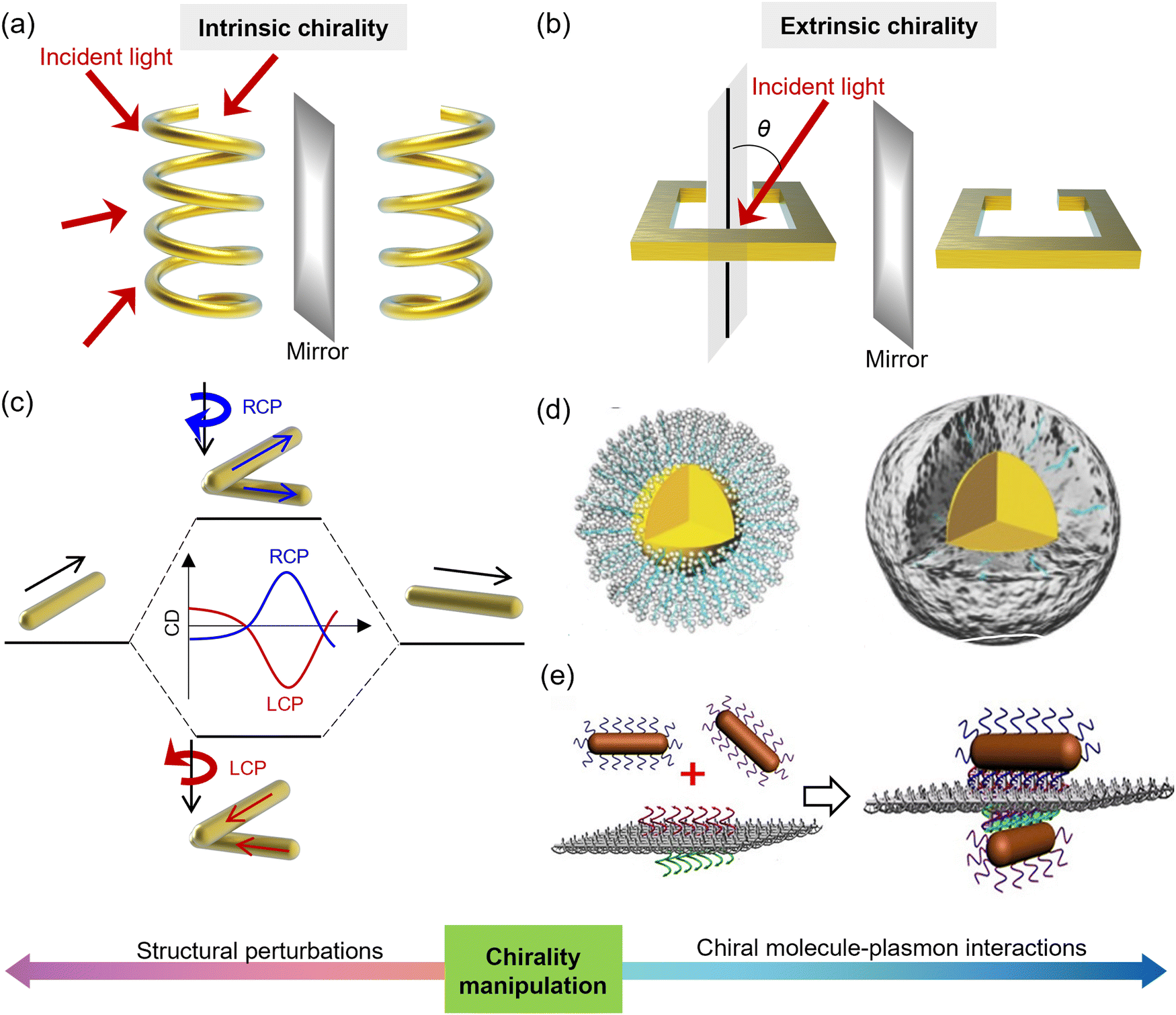 | ||
| Fig. 8 Strategies for achieving plasmon-enhanced chirality. (a) Schematic view of intrinsic 3D chirality using plasmonic spring-shaped nanostructures. (b) Schematic view of extrinsic 3D chirality using a plasmonic split ring resonator. (c) Designing plasmonic chirality via structural perturbations. (d) Designing plasmonic chirality via interactions between chiral matter and plasmonic structures. Adapted with permission from ref. 113; Copyright 2014 John Wiley and Sons. (e) Fabrication of chiral nanostructures using double-sided DNA origami. Adapted with permission from ref. 114; Copyright 2013 American Chemical Society. | ||
Next, we introduce two strategies for manipulating chirality: plasmonic structural perturbation and interaction with chiral molecules. Structural perturbation involves inducing a strong chiral optical response by altering the structure within the plasmonic system, as illustrated in Fig. 8c. In such systems, the chirality of the dimeric plasmonic nanorods is determined by the overall system's chirality rather than that of individual nanorods, because the chiral signal from the dimeric system significantly exceeds that of single nanorods. When coupled with chiral molecules, the dimeric nanorod system exhibits stronger and broader chiral responses compared to single nanorods.115 This plasmonic chirality can be explained by plasmon hybridization theory, which provides an intuitive understanding of how plasmonic modes in coupled nanoparticles interact (Fig. 8c).116,117 This theory explains the splitting of isolated plasmonic modes into bonding and antibonding states. However, the accuracy of this theory diminishes as the system size increases, due to its reliance on an electrostatic approach. Another method to manipulate chirality is through plasmonic interaction with chiral molecules. For achiral nanoparticles, when chiral molecules assemble on their surface, the entire system becomes chiral, effectively enhancing the weak chirality of the molecules. For instance, Wu et al. utilized a DNA-template growth process to create gold core-DNA-silver shell nanoparticles (Au/(DNA-Ag) core–shell NPs), as shown in Fig. 8d.113 They used cytosine-rich single-stranded DNA to guide the growth of the silver shell around the gold core. The resulting nanoparticles exhibited intense and robust chiroptical responses at the silver plasmon band, with a high anisotropy factor.
There are two primary fabrication methods for realizing plasmonic chirality: top-down and bottom-up techniques.118–120 Top-down techniques include electron-beam lithography (EBL), focused ion beam (FIB) milling, photolithography, reactive ion etching (RIE), and others.120 These methods start from a bulk structure and create nanoscale designs through lithography, etching, and deposition, making them more suitable for fabricating nanostructures with intrinsic chirality. Bottom-up techniques include chemical synthesis, ALD, and self-assembly.120 Self-assembly is a notable approach within this category,121 employing chiral templates, discrete DNA strands, and DNA origami templates to organize metal nanoparticles into chiral plasmonic assemblies. Chiral templates, such as biomacromolecules and polymers,122 are powerful tools for guiding the formation of plasmonic nanostructures with strong chiral responses on a large scale. Self-assembly with discrete DNA strands leverages the highly specific interactions between complementary DNA sequences to create rationally programmable DNA nanostructures, where the distances between particles can be precisely controlled by the lengths of the DNA linkers. DNA origami templates involve the folding of a long DNA scaffold strand by using hundreds of designed short oligonucleotides. For example, Lan et al. used bifacial DNA origami as a template to direct the self-assembly of gold nanorods (AuNRs) into 3D nanoarchitectures (Fig. 8e).114 They finely tuned the spatial configuration by adjusting the location of the AuNRs on the origami template, successfully creating discrete 3D nanorod dimer nanoarchitectures with tailored optical chirality.
2.6 Plasmonic waveguide resonance
Optical waveguides are essential components in fiber optic and photonic integrated circuit technologies, benefiting significantly from active photon manipulation to enhance their passive guidance mechanisms.123–129 Emerging applications, such as PICs, demand faster nanoscale waveguide circuits that facilitate stronger light–matter interactions and lower power consumption.130,131 However, all-dielectric waveguides face inherent limitations in miniaturization, restricted to approximately half the wavelength in the dielectric. If the waveguide's lateral dimensions fall below this threshold, light is no longer tightly confined within the waveguide and begins to leak out.True nanoscale modal confinement can only be achieved using metals. In this configuration, photons couple with oscillating charges on the metal surface, forming surface plasmons with an effective modal area that is significantly smaller, i.e., several orders of magnitude below the diffraction limit. This results in extreme confinement, albeit with substantial linear optical losses due to intrinsic electronic damping. Despite this drawback, metallic waveguides are considered revolutionary platforms capable of addressing the inherent limitations of all-dielectric nonlinear devices.
There are three classes of chip-scale plasmonic structures: plasmonic slab waveguides, plasmonic slot waveguides, and hybrid plasmonic waveguides. As shown in Fig. 9a, the plasmonic slab waveguide consists of a dielectric–metal–dielectric structure.132 The thickness of the metal layer significantly affects the modes and propagation of SPPs. For a thick metal layer, it behaves like a semi-infinite metal/dielectric interface that supports transverse magnetic (TM) SPP modes. The penetration depth of SPPs in the metal is determined by the frequency of the incident light (upper panel of Fig. 9b). In the near-infrared range, the electric field is weakly confined transversely on the metal, with a metal penetration depth of 20–30 nm. For visible light wavelengths, the TM confinement of the electric field becomes stronger, resulting in local intensity enhancement. This weak field confinement at longer wavelengths limits the use of bulk SPP-based waveguides in applications such as PICs.133 Therefore, significant research has been conducted to achieve field enhancement by reducing the waveguide dimensions to subwavelength sizes. At this scale, the two supported SPP modes on either side of the film can couple through their evanescent tails, generating antisymmetric and symmetric modes (lower panel of Fig. 9b), known as short-range (SR) and long-range (LR) SPPs, respectively. The responses of SR-SPPs and LR-SPPs to changes in metal thickness differ.134 As the metal thickness increases, the loss of SR-SPPs increases and the near-field confinement becomes weaker. Conversely, for LR-SPPs, the loss decreases and the near-field confinement becomes stronger with increasing metal thickness. Metals can be as thin as a single nanowire. For instance, O’Carroll et al. developed a plasmonic waveguide based on nanoscale single nanowires using a melt-assisted wetting method with porous alumina templates.135 These nanowires exhibit blue photoluminescence under ultraviolet (UV) illumination and can function as nanoscale active optical waveguides, allowing photoluminescence to propagate along the wire and out-couple at the tips.
 | ||
| Fig. 9 Strategies for achieving plasmon-enhanced waveguides. (a) Schematic view of plasmonic slab waveguides. (b) Schematic of the bulk SPP (upper panel), short-range SPP (lower left panel), and long-range SPP (lower right panel). (c) Example of a plasmonic single-nanowire waveguide. Adapted with permission from ref. 135; Copyright 2007 John Wiley and Sons. (d) Schematic view of plasmonic slot waveguides. (e) Example of plasmonic slot waveguides. Adapted with permission from ref. 136; Copyright 2020 Springer Nature. (f) Color-coded electric field of the slot waveguides. (g) Schematic view of hybrid plasmonic waveguides. (h) Example of hybrid waveguides. Adapted with permission from ref. 13; Copyright 2008 Springer Nature. (i) Electromagnetic energy density distributions for hybrid waveguides with different gap size. | ||
Plasmonic slot waveguides consist of a sub-wavelength air slot flanked by two optically thick gold films, as illustrated in Fig. 9d. When the metal/air SPP modes on either surface are brought close together, they couple to form symmetric and anti-symmetric modes.137 The symmetric mode, in particular, produces sub-wavelength lateral confinement and a low group velocity. As the gap size increases, the loss of slot waveguides increases, and the near-field confinement becomes weaker. For instance, Thomaschewski et al. developed a plasmonic slot waveguide consisting of two gold nanostripes on lithium niobate substrates (Fig. 9e).136 This waveguide supports two quasi-transverse electromagnetic (quasi-TEM) modes, specifically the odd and even modes, propagating along the gap. Due to the lithium niobate substrate, ultra-compact switching and modulation functionalities can be achieved by applying a voltage across the gap. This design achieves a 90% modulation depth with a 20-μm-long switch, owing to the strong overlap of slow-plasmon modes and electrostatic fields (Fig. 9f). Additionally, the waveguide exhibits a flat frequency response up to 2 GHz and a 3-dB bandwidth of 9 GHz, indicating its potential for high-speed optical communication applications.
Hybrid plasmonic waveguides, which often utilize multiple materials in intricate configurations, aim to minimize losses while maintaining nanoscale confinement. As illustrated in Fig. 9g, a typical hybrid waveguide consists of a dielectric waveguide adjacent to a metal, separated by a low-index spacer. By adjusting the spacer thickness, this design can balance the advantages of low losses and high confinement. For example, Oulton et al. developed a hybrid waveguide comprising a dielectric nanowire separated from a metal surface by a nanoscale dielectric gap, allowing for subwavelength optical confinement and long-range propagation (Fig. 9h).13 This approach enables subwavelength transmission with strong mode confinement and long propagation distances, surpassing the performance of conventional plasmonic waveguides. The confined hybrid mode's size is more than 100 times smaller than the area of a diffraction-limited spot.
2.7 Section summary
In summary, this section introduces and analyzes the optical multi-effects of plasmons. We explore a range of phenomena, including plasmon–phonon coupling, plasmonic nonlinear optical effects, EIT, plasmonic chirality, plasmonic nanocavity resonance, and plasmonic waveguide resonance. Through this detailed examination, we demonstrate how fundamental plasmonic effects can evolve into complex optical multi-effects, embodying the integration of multiple optical phenomena. Nevertheless, these optical multi-effects continue to present challenges.First, designing multi-functional nanostructures is a critical challenge in plasmonics, especially when aiming to integrate multiple optical effects and others within a single platform. The primary difficulty lies in creating nanostructures that can simultaneously support and optimize multiple plasmonic modes, each of which may have different spatial, spectral, and material requirements. Achieving this requires intricate design processes and precise material engineering, where the physical and chemical properties of the nanostructures must be finely tuned to ensure that the desired effects can coexist without unwanted interference. For instance, Ag nanoparticles and graphene nanoribbons are combined to create a multi-functional substrate capable of enhancing both SERS and SEIRAS.138 This achieved significant EF for both SERS (up to 105) and SEIRAS (up to 170 times), enabling the extraction of complementary vibrational modes from molecules. Other integration strategies for multi-functional nanostructures could be layered structures, hybrid nanomaterials, tunable nanostructures, and multi-modal resonators. Specifically, for layered structures, one layer might be engineered to excite plasmons, while another is designed to excite phonons. By carefully controlling the thickness and material composition of each layer, it is possible to create a structure that supports both effects without significant cross-talk or interference.47 Besides, tunable nanostructures are designed to allow dynamic control over their plasmonic properties. By using materials that can change their optical characteristics in response to external stimuli (e.g., electric fields, temperature, or chemical environment), these structures can be adjusted to optimize different plasmonic effects as needed. This tunability is particularly useful in applications where the conditions of measurement may vary, requiring different optical effects to be prioritized at different times. In terms of multi-modal resonators, they can support different resonant frequencies corresponding to different optical effects. The key challenge here is to design the resonator geometry in such a way that the different modes do not interfere with each other, while still providing strong field enhancement for each effect.
Second, effect synergy and optimization are also challenging. Integrating multiple optical effects in plasmonic nanostructures requires not only the individual optimization of each effect but also ensuring that these effects work synergistically when combined. Effect synergy refers to the ability of different plasmonic effects—such as SERS, SEF, and LSPR—to enhance each other's performance when integrated into a single platform. However, achieving this synergy is challenging due to the distinct and sometimes conflicting requirements of each effect. Specifically, one challenge in achieving synergy could be conflicting design requirements. Each plasmonic effect typically has specific design requirements that may conflict with those of other effects. For example, SERS often requires sharp metallic nanostructures with high curvature to generate intense localized electromagnetic fields, while SEF might require broader surfaces or different geometries to optimize fluorescence signal enhancement. Balancing these conflicting requirements in a single nanostructure is a major challenge in effect synergy. Besides, synergistic enhancement typically requires that the different effects operate within the same spectral and spatial regions. However, the resonant conditions for different effects might not naturally overlap. For instance, SERS and LSPR might occur at different wavelengths, necessitating careful tuning of the nanostructure's geometry and material properties to bring these effects into spectral alignment.
Third, balancing the spatial distribution is challenging. Field localization and distribution refers to the concentration of electromagnetic fields in a small region, often at the surface of a metallic nanostructure, where the field intensity can be orders of magnitude higher than that in the surrounding medium. This localized enhancement is crucial for amplifying weak optical signals, making it a key aspect of plasmonic devices. The challenge in field localization and enhancement lies in balancing the spatial distribution of the localized fields across the nanostructure. Different plasmonic effects often require specific spatial configurations of the enhanced fields. For instance, SERS typically benefits from “hot spots”—regions of extremely high field intensity at sharp features or junctions between nanoparticles—while other effects, such as SEF, may require a more uniform field distribution over a larger area. Achieving the right balance in the spatial distribution is challenging because it requires precise control over the nanostructure's geometry, size, and material composition.
3. Mechanics of plasmonic optical-electric-acousto-thermal fusion
3.1 Plasmonic fusion with electronics
The combination of plasmonics and electronics is achieved using hot electrons as a “bridge”. The process associated with hot electrons includes plasmon generation and decay, and hot-electron generation, injection, and regeneration (Fig. 10a). The excitation and decay of plasmon have been introduced in the previous article. Plasmons are excited by incident light of a specific frequency and they dissipate their energy through radiative and non-radiative decay. The decay process is related to hot electrons, which can be traced back to 1996, when Zhao et al. observed the photocurrent in the TiO2 anode by irradiating TiO2 electrodes covered with gold or silver nanoparticles with visible light.139 This is a surprising result because conventional TiO2 generates photocurrent only when illuminated by UV light. The mechanism by which TiO2 generates photocurrent under visible light irradiation is still unclear. In 2003, the mechanism was ascribed to plasmon-induced charge separation and oxidation by Ohko et al.140 Subsequent studies demonstrated the three processes required to generate the photoinduced current: hot electron generation, injection, and regeneration.141,142 Following these pioneering studies, plasmonic hot electrons have been widely used in photovoltaic and catalytic devices. Injecting and conducting away hot electrons before carrier recombination is a key factor in the fusion of plasmonics and electronics. A common injection method is to allow plasmon particles to contact a semiconductor (such as TiO2), forming Schottky junctions to extract hot electrons.143 The hot-electron generation and injection in TiO2 can be completed within 50 fs.144 The next step is hot-electron regeneration, which is to harness the energy of hot electrons before they thermalize. This can be done by transferring the energy to a different system. Carrier regeneration using liquid electrolytes or a hole-transporting material is effective. For instance, electron donor solutions containing Fe2+ were demonstrated to accelerate carrier regeneration.145 To further improve the energy conversion efficiency of this process, it is crucial to optimize the donor solution or hole-transporting materials to achieve faster hot electron injection and regeneration before energy loss occurs due to electron–electron collisions.146 | ||
| Fig. 10 Plasmonic fusion with electronics. (a) Schematic view of plasmon generation and decay, hot-electron generation, injection, and regeneration. (b) Plasmonic fusion with electronics via light-trapping, electron transfer, and energy transfer. | ||
Surface plasmons are collective vibration modes of free electrons under optical excitation, which have the potential to combine electrical effects naturally. Plasmon-based electrical effects offer clear benefits in applications involving light-trapping, electron transfer, and energy transfer (Fig. 10b).147 For instance, the enhanced light-trapping capability is advantageous for plasmon-based electrical applications, such as photodetectors, solar cells, and photocatalysis.148–152 These applications involve energy harvesting and electron transfer.153 Therefore, we next examine these processes in detail.
 | ||
| Fig. 11 Plasmonic light-trapping mechanism. (a) Schematic view of the mechanism, including the plasmonic light scattering effect (left panel), the excitation of plasmons in nanoparticles embedded in the semiconductor (middle panel), and the excitation of plasmons at the metal/semiconductor interface (right panel). (b) Performance of solar cells with/without plasmonic light-trapping. Adapted with permission from ref. 154; Copyright 2008 AIP Publishing. (c) Effect of plasmonic structure shape on light trapping. Adapted with permission from ref. 155; Copyright 2008 AIP Publishing. | ||
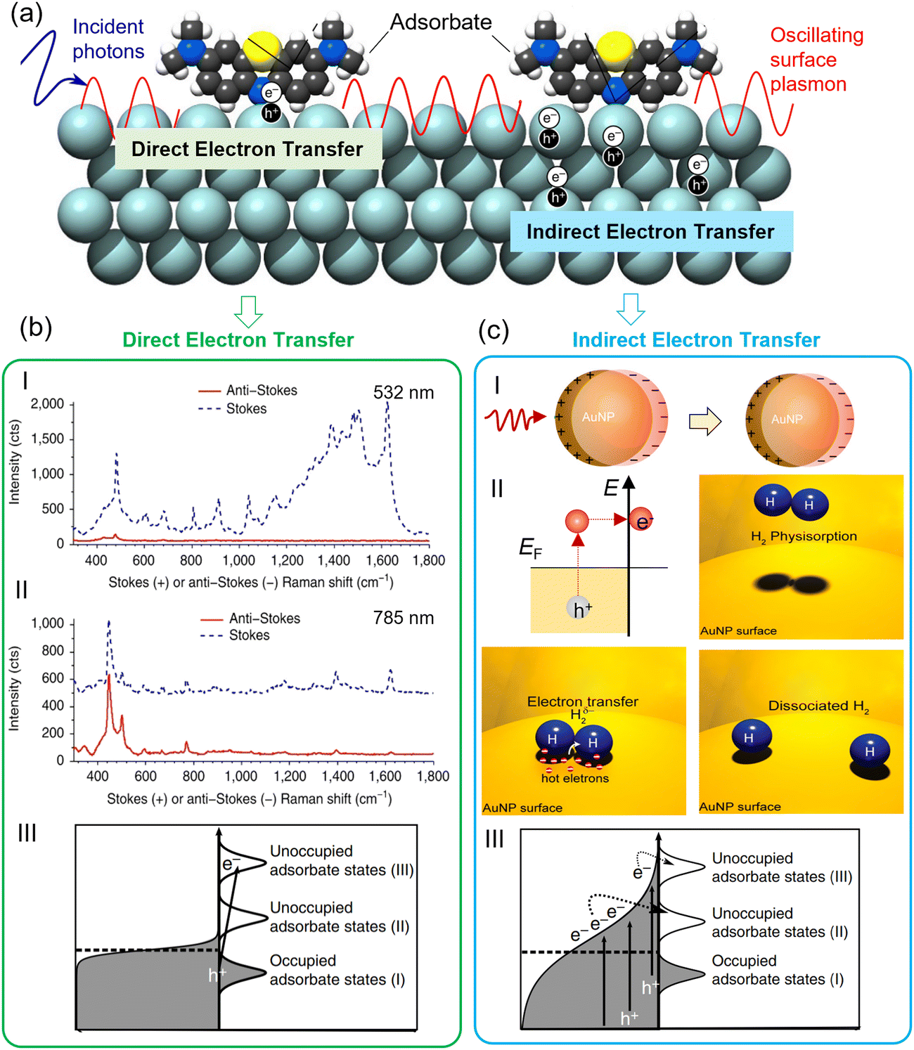 | ||
| Fig. 12 Plasmonic electron transfer mechanism. (a) Schematic view of the metal/adsorbate system. (b) Direct electron transfer mechanism in metal/adsorbate systems. Adapted with permission from ref. 158; Copyright 2016 Springer Nature. (I, II)Raman spectra of methylene blue with excitation wavelengths of (I) 532 nm and (II) 785 nm. (III) Schematic diagram of the energy levels of direct electron transfer. (c) Indirect electron transfer mechanism. Adapted with permission from ref. 159; Copyright 2013 American Chemical Society. (I) Schematics of plasmon-induced hot electron generation on AuNPs. (II) Schematic diagram of H2 dissociation on the AuNP surface. (III) Schematic diagram of the energy levels of indirect electron transfer. | ||
The indirect transfer of hot electrons from metal nanostructures to adsorbed molecules involves a more complex process compared to direct transfer. After the generation, hot electrons undergo a process called thermalization. This involves electron–electron scattering, which redistributes the energy among the electrons, leading to a Fermi–Dirac distribution of hot electrons and holes. In the indirect transfer mechanism, the thermalized hot electrons can spill over from the metal nanostructure into the surrounding environment. This spillover occurs when the hot electrons transiently leave the metal surface and interact with the adsorbed molecules. During the spillover, the hot electrons can transfer their energy to the adsorbed molecules. This energy transfer can destabilize the molecular bonds, facilitating chemical reactions.160 The interaction often leads to the excitation of molecular vibrations, which can lower the activation energy for subsequent reactions. Notably, the indirect transfer process competes with other relaxation mechanisms, such as electron–phonon scattering, which can lead to the loss of hot electrons before they can interact with the adsorbed molecules. Taking the room temperature dissociation of H2 as an example (Fig. 12c),159 surface plasmons excited in the Au nanoparticles decay into hot electrons, which transfer into a Feshbach resonance of an H2 molecule adsorbed on the Au surface, triggering dissociation.
 | ||
| Fig. 13 Plasmonic energy transfer mechanism. (a) Comparison between plasmon-induced resonance energy transfer (PIRET) and Förster resonance energy transfer (FRET). Adapted with permission from ref. 161; Copyright 2015 Springer Nature. PIRET excites the coherent plasmon-to-semiconductor energy-transfer pathway, while FRET experiences an incoherent semiconductor-to-plasmon pathway. Both transfer energy by dipole–dipole coupling. (b) Enhancement of photoconversion by PIRET showing the distance dependence of the dipole–dipole interaction in PIRET. | ||
PIRET involves resonant energy transfer from localized surface plasmons—typically present in metal nanoparticles—to nearby semiconductors. Dominant material systems exploiting the PIRET mechanism include metal–oxide nanostructures29,165,166 (such as Au–TiO2 or Ag–TiO2 heterostructures, as well as combinations like Au–ZnO, Ag–ZnO, and Au–CeO2 used in photocatalysis, solar cells, and sensors), metal–chalcogenide composites (for example, Au–CdS, Au–Cu2O, and Au–ZnS systems that enable visible-light-driven photocatalysis), and alloy nanoparticle–semiconductor configurations (where alloyed plasmonic nanoparticles like Au–Ag or Au–Pd are combined with semiconductors to provide tunable plasmon resonances matching specific semiconductor band gaps, thereby potentially boosting PIRET efficiency). In contrast, FRET describes dipole–dipole coupling between two light-sensitive species, with predominant material systems including organic dye molecules167 (classic FRET pairs like Alexa Fluor dyes, rhodamine derivatives, and cyanine dyes commonly used in bioimaging and sensing due to their high extinction coefficients and well-defined spectral overlaps), quantum dots (semiconductor nanocrystals such as CdSe/ZnS or InP/ZnS that serve as FRET donors or acceptors because of their size-tunable emission spectra and relative photostability), and perovskite nanocrystals (emerging FRET donors or acceptors in hybrid optoelectronics, where lead halide perovskite nanocrystals like CsPbBr3 exhibit bright photoluminescence along with well-defined absorption and emission overlaps for efficient energy transfer).
3.2 Plasmonic fusion with thermonics
Plasmonics, as described above, has a wide range of applications in electronics via hot electron enhancement in areas such as sensing and energy harvesting. In these studies, losses in the metal and the associated heat generation are often considered as side effects that must be minimized. Various strategies have been explored to reduce heat loss.168 One approach involves material optimization, leading to the adoption of alternative plasmonic materials, such as all-dielectric materials, which exhibit lower ohmic losses compared to noble metals.169 Structural engineering techniques, such as metal–insulator–metal configurations, have also been reported to enhance light confinement and reduce non-radiative losses by up to 50%.53 Additionally, advanced resonator designs, including high-Q plasmonic resonators like bound states in the continuum (BIC) in continuous media, have been shown to improve energy confinement and minimize unnecessary heat generation.170 Beyond these strategies, effective thermal management is essential to mitigate plasmonic heating. Excess thermal energy must be dissipated from plasmonic chips through conduction, convection, or radiation.168 A recent study demonstrated a passive cooling system designed for high-performance plasmonic chips, leveraging enhanced thermal conduction and natural convection.171 The results indicate that by integrating conventional cooling methods with well-designed thermal interfaces, self-heating can be significantly reduced, lowering the temperature of the system to a few Kelvins.However, some studies have shown that with appropriate design, plasmon-related heat has great potential in thermal applications, which is called thermoplasmonics.172 In 1999,173 a seminal study utilized gold nanoparticles to generate heat and induce protein denaturation, highlighting the benefits of metal nanoparticles over traditional dyes due to their enhanced light–matter interaction at plasmonic resonance, which creates localized, high-temperature increments without thermobleaching or photobleaching. Despite its innovation, this work initially went unnoticed. Interest in nanoplasmonic heating surged with two key publications: one in 2002 introduced plasmonic photothermal imaging, combining modulated heating of nanoparticles with lock-in detection for precise positioning without photobleaching,174 and the other in 2003 proposed plasmonic photothermal therapy for targeted cancer hyperthermia using gold nanoparticles.175,176 These studies, alongside emerging applications like drug and gene delivery, established thermoplasmonics as a significant field, leveraging plasmonic nanoparticles as nanoscale heat sources for various innovative uses.177–180
Thermoplasmonics deals with the laws of heat generation and diffusion, and its core is not the propagation, interference and diffraction of light that are familiar in the field of optics. Key mechanisms in thermoplasmonics include local heating, radiative heat transfer, and thermal expansion (Fig. 14). Plasmonic nanoparticles can convert absorbed light into localized heat efficiently, which can be utilized for applications such as photothermal therapy and triggering chemical reactions.181 Additionally, plasmons facilitate radiative heat transfer, allowing for efficient energy transfer between nanoparticles and their surroundings, enhancing thermal management in devices. Thermal expansion due to plasmonic heating can be harnessed to actuate nanoscale mechanical systems or to modify the properties of materials at the nanoscale, leading to innovative applications in nanoactuators. Next, we examine these processes in detail.
 | ||
| Fig. 14 Plasmonic fusion with thermionics. The plasmons enhance electronics via local heating, radiative heat transfer, and thermal expansion. | ||
Plasmons undergo nonradiative relaxation via electron–electron collisions or electron-lattice phonon coupling, generating heat and increasing the surrounding temperature. The plasmonic heating process is shown in Fig. 15a.182 When metal nanostructures are excited with resonant photons, the photoexcitation of the electron gas results in rapid non-equilibrium heating. This process begins with the absorption of resonant light, causing collective oscillations of free electrons known as plasmons. These excited electrons quickly undergo electron–electron scattering within subpicosecond timescales, leading to a significant rise in the metal's surface temperature. Following this initial heating, the electrons transfer their energy to the lattice through electron–phonon coupling, bringing the system toward thermal equilibrium. This energy exchange happens rapidly, causing the lattice to heat up. In the subsequent hundred picoseconds, the lattice cools down via phonon–phonon interactions, dissipating heat into the surrounding medium. This mechanism of localized heating and subsequent heat transfer into the environment has wide-ranging applications. In medical treatments like plasmonic photothermal therapy, the generated heat can selectively destroy cancer cells.183 In catalysis, the localized heating can accelerate chemical reactions.184 Moreover, this process is utilized in sensors and imaging technologies, where the heat-induced changes can produce detectable signals.
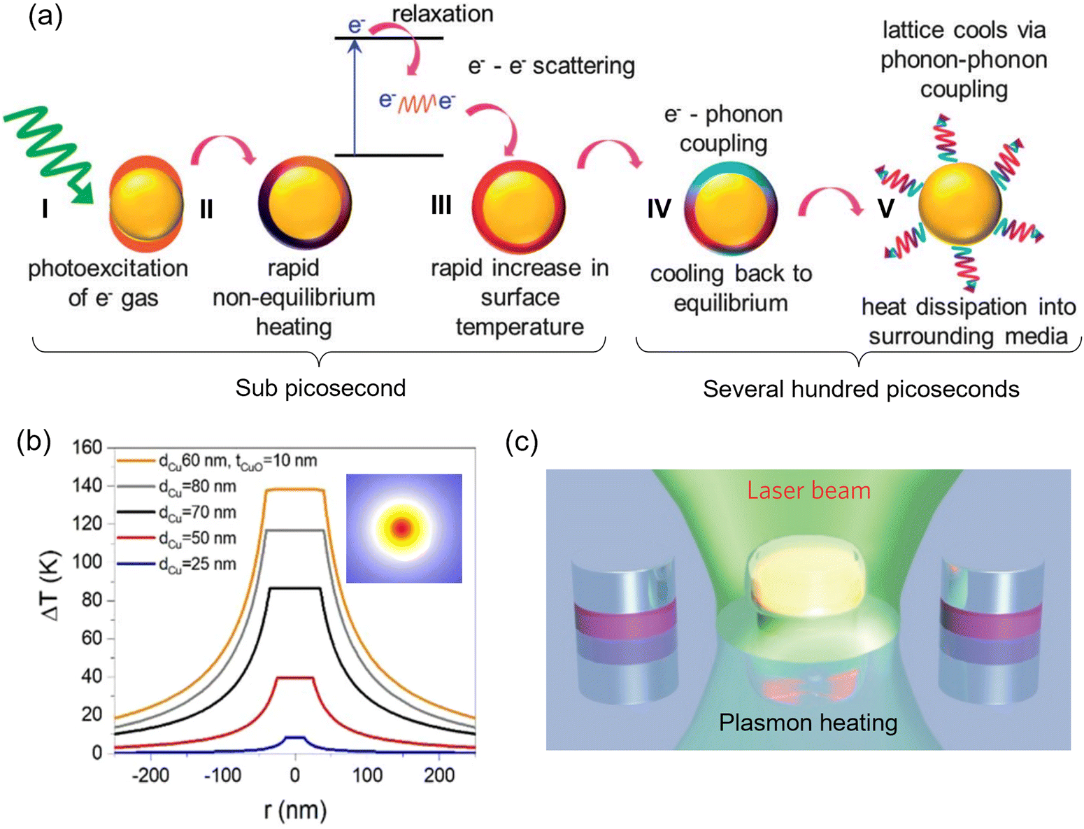 | ||
| Fig. 15 Plasmonic local heating mechanism. (a) Principles of photothermal light conversion into local heat in nanoparticles. Adapted with permission from ref. 182; Copyright 2014 the Royal Society of Chemistry. The plasmonic heating process includes (I) photoexcitation of the electron gas, (II) non-equilibrium heating, (III) increase in the surface temperature, (IV) cooling to equilibrium, and (V) heat dissipation into the surrounding medium. (b) Temperature profile around 25nm (blue), 50nm (red), 70nm (black), and 80nm (grey) solid CuNPs under a constant laser power of 270mW. Adapted with permission from ref. 185; Copyright 2020 Springer Nature. Inset: 2D heat profile of CuNPs. (c) Schematic illustration of the plasmonic heating for nanofabrication. Adapted with permission from ref. 186; Copyright 2016 Springer Nature. | ||
The temperature increase of plasmonic nanoparticles is affected by the laser power and the absorption cross section of nanoparticles. Fig. 15b shows the temperature profiles of three optically trapped CuNPs of different sizes under a constant laser power of 270 mW.185 As observed, the temperature of the particle surface is the same, and the temperature rise decreases in the area away from the particle. In addition, the larger the particle, the higher its temperature. The generated local heating is not limited to being transferred to the surrounding medium, but can also be used to reshape the nanostructure itself. A representative example is plasmonic colour laser printing. As shown in Fig. 15c,186 a laser is used to emit short, intense pulses of light onto the nanoimprinted metasurface, which generates localized heat due to the absorption of light. The localized heating causes the nanostructures to undergo thermal deformation. Depending on the laser parameters, the nanostructures can be reshaped in various ways, such as changing their size, shape, or orientation. The reshaping of the nanostructures alters their plasmonic properties, which in turn changes the way they interact with light. By precisely controlling the reshaping process, different colors can be produced. This is because the plasmonic resonances of the nanostructures determine the specific wavelengths of light they absorb and scatter. The method allows for extremely high-resolution color printing, with a resolution of up to 127000 dots per inch (DPI). This is due to the precise control over the laser pulses and the nanoscale features of the metasurfaces.
In addition to thermal conduction, another way of heat transfer is near-field radiative heat transfer (NFRHT). This phenomenon arises when the distance between two objects is comparable to or less than their characteristic thermal wavelength, allowing energy to transfer through evanescent waves, such as frustrated modes and surface polaritons. Consequently, the heat flux in the near-field can be significantly greater than that of conventional far-field radiation. NFRHT becomes particularly pronounced when objects are separated by a vacuum gap smaller than their thermal characteristic wavelength. Research into NFRHT has uncovered intriguing effects, such as ballistic heat transport, thermal photon drag, and an unusual photon thermal Hall effect.187 This line of study has led to innovative applications, including the development of thermophotovoltaic devices, near-field radiative cooling systems, and advanced thermal management solutions. Next, we introduce NFRHT by taking a system consisting of two monolayer bismuth selenide (Bi2Se3) sheets as an example, as shown in Fig. 16a.188 The heat flux between them and their comparison with ITO and graphene are shown in Fig. 16b. For nanoscale gaps, the NFRHT between two Bi2Se3 sheets is greatly enhanced, and its magnitude can be well above the blackbody limit. Moreover, the heat flux between Bi2Se3 sheets can exceed that of monolayer graphene and bulk ITO, especially at smaller gap distances. For NFRHT, the heat transfer distance is a key parameter. As the distance increases, the radiative heat flux of a single-layer Bi2Se3 sheet decreases monotonically due to the rapid decay of the localized density of states, and the corresponding NFRHT also decreases rapidly. In addition, the spectral radiation heat flux redshifts with increasing gaps (Fig. 16c). This redshift of the spectral radiation heat flux can be explained by the attenuation length, that is, surface polaritons located at high frequencies are more easily filtered out by larger vacuum gaps.189
 | ||
| Fig. 16 Plasmonic radiative heat transfer mechanism. (a) Schematic of near-field radiative heat transfer between two sheets of bismuth selenide (Bi2Se3). (b) Heat flux Q of the monolayer Bi2Se3 sheet, monolayer graphene sheet, and bulk ITO, with different vacuum gaps. (c) Heat flux Q as a function of incident light frequency (ω) for two sheets of Bi2Se3 under different gaps d. Adapted with permission from ref. 188; Copyright 2021 Elsevier. | ||
Thermal expansion caused by uneven heating is another thermal feature. Nanostructures such as nanorods and nanowires have an uneven near-field distribution due to the lightning rod effect, which leads to spatially distributed heat. Uneven thermal expansion is widely used in actuators. The concept of using plasmonic thermal expansion for actuation emerged due to the potential for precise and rapid control of mechanical movements at the micro- and nano-scale. Early demonstrations involved simple structures, such as cantilevers and membranes,190 incorporating plasmonic materials that expanded upon light irradiation. In the 2010s, significant progress was made in developing plasmonic actuators.191,192 Complex nanoscale devices that utilized plasmonic thermal expansion to achieve controlled movements were developed.193 These actuators demonstrated high precision, fast response times, and the ability to operate at small scales. For instance, Linghu et al. demonstrated the plasmon-driven movement of gold nanowires on silica microfibres (Fig. 17a).194 Specifically, plasmons are excited in metal nanowires using pulsed lasers, enhancing the heating effect and generating surface acoustic waves (SAWs). The heating causes the nanowire to expand and contract, creating a peristaltic crawling motion similar to an earthworm (Fig. 17b). The SAWs help the nanowires overcome strong surface adhesion forces, allowing precise movement along silica microfibres (Fig. 17c). This method achieves sub-nanometer positioning accuracy, low actuation power, and versatile on-chip manipulations (Fig. 17d and e).
 | ||
| Fig. 17 Plasmonic thermal expansion. (a) Schematic diagram of the peristaltic crawling caused by thermal expansion of plasmons. Adapted with permission from ref. 194; Copyright 2021 Springer Nature. (b) Time-course changes of the nanowire in the thermal crawling. (c) Time-dependent axial expansion behavior of the nanowire front end. (d) The creeping movement of gold nanowires on silica microfibers due to thermal expansion. (e) Microscope image showing the movement of gold nanowires on suspended microfibers. | ||
Combining plasmonic nanoparticles with soft materials is another strategy to exploit thermal expansion. For instance, a bilayer structure combining gold nanoparticles with poly(N-isopropylacrylamide) and poly(acrylamide) was developed.195 This system leverages the heating of gold nanoparticles upon exposure to their plasmon resonance wavelength, leading to differential thermal expansion between the two layers. Plasmonic resonances are particularly useful for achieving wavelength-specific responses. For example, an actuator utilizing AuNRs on polymethyl methacrylate (PMMA) was designed,191 where careful tuning of the nanorods' dimensions allowed for sensitivity to various wavelengths in the visible and near-infrared spectra. Similarly, a wavelength-dependent actuator was developed by embedding copper nanorods in a PVA matrix.193 In contrast, highly damped plasmonic nanostructures can be engineered for an ultrabroadband light response. This was exemplified by mechanically coupled arrays of iron nanodomes transferred onto thin polydimethylsiloxane (PDMS) layers, creating soft actuators responsive to light from UV to thermal infrared.196 Applications of this technology include a self-regulating iris, an optical gripper, and an opto-mechanical electrical switch. Furthermore, a magnetic-plasmonic actuator consisting of hybrid Fe3O4/Ag nanorods within a photocurable polymer matrix was developed and modulated by altering the laser polarization.197
3.3 Plasmonic fusion with acoustics
The combination of plasmonics and acoustics represents a promising frontier in the field of wave-based technologies. Plasmons are renowned for their ability to manipulate light at the nanoscale, concentrating electromagnetic energy in tiny volumes. When these capabilities are harnessed alongside acoustic waves—mechanical vibrations that propagate through different media—the result is a powerful synergy that enhances the performance of acoustic systems across a wide range of frequencies. This integration not only addresses existing challenges in acoustics but also opens up new possibilities for applications in sensing, imaging, and fluid control. By exploring the interactions between plasmons and acoustics across different frequency ranges, we can unlock new levels of precision and efficiency in various technologies.The combination of plasmons and acoustics covers the kHz to IR region (Fig. 18). In the kHz range, ultrasound struggles with the limited efficiency of generating and detecting ultrasound waves, particularly in applications involving the PA imaging of biological tissues in vivo. Plasmons, with their ability to generate local heating via hot electrons, significantly enhance PA effects by increasing transient thermoelastic expansion. The critical technology here involves the design of plasmonic nanostructures that resonate at the specific wavelengths used in PA applications, optimizing light absorption and conversion into ultrasound waves. Moving to the MHz range, plasmons can enhance the detection of microfluidic behavior by improving the sensitivity of sensors that interact with SAWs. This allows for more precise monitoring of fluid dynamics, while SAWs themselves are used to control the movement of these fluids.198 This involves engineering plasmonic surfaces that can interact effectively with SAWs, enabling simultaneous detection and control within microfluidic environments. In the GHz range, a significant challenge is the excitation and detection of high-order acoustic modes, which are difficult to resolve due to their ultrafast nature. When combined with femtosecond pump–probe techniques, plasmons enable the excitation and detection of these high-order modes in thin metal films, particularly in LO acoustic modes. The plasmonic enhancement improves temporal resolution and sensitivity, making it possible to study these fast acoustic phenomena. At even higher frequencies, in the THz to infrared range, the proximity of graphene to metals can give rise to graphene acoustic plasmon resonance, which provides a novel mechanism for enhancing acoustic interactions in this spectral range. This phenomenon opens up new possibilities for acoustic manipulation and sensing in the THz to IR range. Overall, across all these frequency ranges, the integration of plasmonics with acoustics offers innovative solutions to longstanding challenges. Next, we examine these combinations in detail.
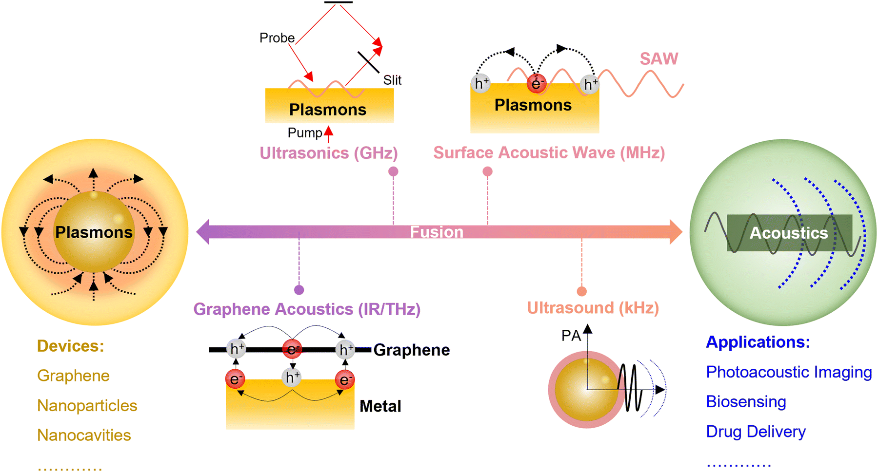 | ||
| Fig. 18 Plasmonic fusion with acoustics. The combination of plasmon and acoustic devices includes ultrasound in the kHz region, SAWs in the MHz region, ultrasonics in the GHz region, and graphene acoustics in the IR/THz region. | ||
In the kHz range, plasmonic effects predominantly enhance the PA effect. Four main mechanisms for the generation of PA waves have been reported: thermal expansion or thermoelastic expansion, vaporization, optical breakdown, and photochemical processes. For biomedical applications, the thermoelastic expansion route is generally considered the mainstream strategy, induced by a slight temperature increase (usually in the millikelvin range) due to energy deposition inside biological tissues through the absorption of incident electromagnetic energy.199 The excited PA signal is locally determined by the electromagnetic absorption and scattering properties, thermal properties (including thermal diffusivity and thermal expansion coefficient), and elastic properties of the sample. The plasmonic enhancement of the PA signal arises because plasmons can significantly increase the efficiency of light absorption and subsequent heat generation. The generation of ultrasound enhanced by plasmonic nanoparticles is shown in Fig. 19a. First, plasmons are excited by the irradiation of a pulse of light, which causes local heating. Due to the small increase in temperature caused by the absorption of heat, the plasmonic particles expand briefly. This generates a pressure transient that can be detected acoustically. There is no bulk heating of the sample because the expansion is spatially and thermally confined using light pulses shorter than the thermal relaxation time of the absorber.
 | ||
| Fig. 19 Plasmon-enhanced photoacoustic effects in the kHz range. (a) Schematic diagram showing the enhancement of ultrasound generation in photoacoustic effects via the pressure difference induced by plasmon-enhanced thermal expansion. (b) Factors affecting pressure difference (ρo) in plasmon-enhanced photoacoustic effects. (c) Schematic diagram of the plasmon-enhanced photoacoustic imaging. Adapted with permission from ref. 200; Copyright 2021 American Chemical Society. | ||
The resulting PA signal is a function of the optical, thermal, and elastic properties of the nanoparticle–medium system, which can be expressed by (Fig. 19b)
 | (5) |
Regarding the coefficient of thermal expansion (β), it is a material property that describes how the size of an object changes with temperature and is generally challenging to alter in plasmonic nanostructures. However, β can be influenced by interfacial thermal resistance. During laser pulsing, heat is not fully confined within nanoparticles; instead, some heat diffuses into the surrounding solvent, creating a high-temperature shell-like solvent layer around the nanoparticles. This temperature rise causes thermal expansion in both the nanoparticles and the solvent. The amount of heat transferred to the solvent is determined by factors such as the laser pulse duration, the interfacial thermal resistance at the nanoparticle–solvent boundary, and the thermoelastic properties of the solvent. Thus, modifying solvent properties emerges as a viable approach to enhancing the PA signal. For instance, Shi and collaborators demonstrated through modeling and experimentation that replacing water with ethanol as the solvent for gold nanospheres increased the PA signal by a factor of 4.5.202
In the MHz range, there are two strategies to achieve the combination of plasmons and SAWs, depending on the way of plasmon excitation. The first approach is the interaction of SAWs with plasmons in optical waveguides with confined modes, as shown in Fig. 20a. In this configuration, SAWs can modulate the local dielectric environment and the electron density at the metal surface, leading to a periodic modulation of the plasmon resonance. This interaction can be used to dynamically tune the plasmonic response in a material, potentially allowing for the development of reconfigurable plasmonic devices. Besides, the mechanical strain and the electric fields generated by SAWs can enhance the propagation of surface plasmons along the interface, possibly leading to increased plasmonic signal strength over longer distances. For instance, Huang and co-workers integrated a semiconductor–metal–insulator–semiconductor based hybrid plasmonic waveguide with interdigital transducers for SAW generation (Fig. 20b).203 It is demonstrated that SAWs can cause periodic refractive index variations along the direction of acoustic propagation (Fig. 20c). This phenomenon can be understood by considering the refractive index modulation caused by the elastic deformation induced by SAWs. Besides, the plasmonic intensity was also enhanced by the SAW, and it achieves a plasmonic intensity gain of 1.08 dB at a peak-to-peak potential swing of 3 V.
 | ||
| Fig. 20 Integration strategy of plasmons and surface acoustic waves (SAW) in the MHz range. (a) Schematic diagram showing the integration of plasmons and SAWs in confined modes. (b) An example illustrating the integration of SAWs with propagating SPPs via a plasmonic waveguide in confined modes. Adapted with permission from ref. 203; Copyright 2024 Springer Nature. (c) The cross-sectional view showing the plasmonic waveguide-SAW platform. (d) Schematic diagram showing the integration of plasmons and SAWs in free-space excitation. (e) An example illustrating the integration of SAWs and SPRs in free-space excitation. Adapted with permission from ref. 204; Copyright 2010 the Royal Society of Chemistry. (f) Refractive index-sensitive behavior of the SAW-SPR platform. | ||
The second approach is the interaction of SAWs with plasmons in free-space excitation, as shown in Fig. 20d. In this configuration, the combination leverages the high sensitivity of plasmonic sensors to changes in the refractive index at the sensor surface, along with the ability of SAWs to manipulate and control fluids at the microscale. A specific example of this integration is the use of a common LiNbO3 piezoelectric substrate, where SPR sensing is combined with SAW actuation (Fig. 20e).204 In this setup, the LiNbO3 substrate facilitates the generation of SAWs due to its piezoelectric properties. These acoustic waves can then interact with the surface plasmon waves, leading to enhanced microfluidic mixing on the sensor surface. This enhanced mixing is crucial in scenarios where rapid and uniform distribution of analytes is needed, such as in biosensing assays. Additionally, the SAW component can help reduce non-specific adsorption of molecules to the sensor surface. Non-specific adsorption often leads to false positives or reduced sensitivity in SPR sensors. By using SAWs, the surface can be actively cleaned or modulated, which helps in maintaining the specificity and accuracy of the SPR signal. This combination not only improves the sensitivity and selectivity of the sensor but also enhances the overall performance by reducing noise and improving the response time (Fig. 20f).
In the MHz range, the integration of plasmonics with ultrafast ultrasonics, particularly pico/femtosecond ultrasonics, offers significant advancements in the field by enhancing both the generation and detection of high-frequency acoustic waves. Plasmons can confine electromagnetic fields to nanoscale regions, which amplifies the interaction between light and matter. This confinement is crucial for ultrafast ultrasonics, where the ability to generate and detect acoustic waves with high spatial resolution and sensitivity is essential. The setup for ultrafast ultrasonics involves a pump–probe technique, as shown in Fig. 21a, where a short laser pulse (pump) is used to excite the material and generate acoustic waves, and a delayed pulse (probe) is used to detect the resulting changes. In the setup, the process begins with the pump beam being focused onto a gold layer from the air side, creating a localized thermal expansion that generates picosecond acoustic waves within the material. To improve the accuracy of the measurements, a portion of the probe beam is split off and used in a balanced detection scheme.
 | ||
| Fig. 21 Plasmon-enhanced pico/femtosecond ultrasonics in the GHz range. (a) Schematic of the pump–probe setup for GHz acoustics. (b) Time domain signal of the plasmonic ultrasonics with picosecond acoustic pulses. Adapted with permission from ref. 205; Copyright 2023 Elsevier. (c) Corresponding Fourier spectra in the frequency domain. (d) Schematic of femtosecond plasmonic ultrasonics in a hybrid gold–cobalt multilayer structure. Adapted with permission from ref. 206; Copyright 2013 Springer Nature. (e) Measured interferogram of the hybrid structure showing a shift of the interference fringes upon reflection of an ultrashort acoustic pulse. (f) Time domain signal of the hybrid structure showing femtosecond time-resolved response. | ||
One of the primary enhancements that plasmonics brings to picosecond ultrasonics is the ability to focus energy into extremely small volumes, leading to the generation of more intense and localized acoustic waves. This is particularly useful in applications involving nanoparticles or nanostructured materials, where traditional methods might struggle to achieve sufficient excitation or detection sensitivity. In terms of detection, plasmonic enhancement can significantly improve the sensitivity to small changes in optical properties caused by acoustic waves. This is particularly important in cases where the acoustically induced changes are subtle, such as in nanoscale systems or materials with weak acoustic responses. Plasmons, by amplifying these changes, enable more precise measurements. For instance, Hettich and co-workers combined ultrafast pump–probe PA spectroscopy with plasmon resonance to detect LO acoustic modes in gold films.205 The method achieved high sensitivity, detecting acoustic modes up to the 7th harmonic (∼200 GHz) with sub-picometer amplitude sensing capabilities (Fig. 21b and c). It also separated the dynamics of the dielectric function and film thickness variation. To extend ultrasonics from picosecond to femtosecond, Temnov and co-workers developed a hybrid gold/cobalt bilayer structure using ultrafast surface plasmon interferometry with femtosecond time resolution (Fig. 21d).206 They observed substantial nonlinear reshaping of acoustic pulses after propagating just 100 nm in gold (Fig. 21e and f).
In the terahertz to infrared range, a mode called acoustic graphene plasmon (AGP) with unprecedented field confinement can be excited. Its excitations can be traced back to graphene plasmons, which are collective oscillations of charge carriers in graphene, which can be excited by electromagnetic fields, particularly in the IR and THz frequency ranges. These graphene plasmons are known for their ability to confine electromagnetic energy into extremely small volumes, enabling strong light–matter interactions at the nanoscale. However, when graphene is brought close to a metal surface, with a sufficiently thin dielectric spacer in between, a different type of plasmon, known as the AGP, can be excited (Fig. 22a). The AGP arises from the interaction between the charge density oscillations in the doped graphene layer and the image charges induced in the nearby metal. This interaction effectively mirrors the oscillating charges in graphene, leading to a highly confined plasmonic mode within the narrow dielectric spacer. Unlike conventional graphene plasmons, AGPs are characterized by their ability to propagate with a much higher wavevector, allowing for extreme localization of the electromagnetic field.
 | ||
| Fig. 22 Graphene acoustic plasmon in the THz to IR range. (a) Schematic diagram of the acoustic graphene plasmon. From top to bottom: Schematic diagram of the electric field decay, charge displacement, and electric field lines along the z direction of the metallic graphene plasmons and AGPs. (b) Strong light confinement in the graphene acoustic plasmon. Adapted with permission from ref. 207; Copyright 2021 Springer Nature. (c) Utilizing conventional graphene plasmons as an intermediary and integrating an optical spacer and a back reflector to excite AGPs for high absorption of incident light, ultrasensitive detection of Ångström-thick protein and dielectric films is achieved. Adapted with permission from ref. 208; Copyright 2019 Springer Nature. | ||
One of the key properties of AGPs is their unprecedented field confinement (Fig. 22b),207 which surpasses that of traditional graphene plasmons and other polaritonic modes in van der Waals materials. This confinement occurs primarily within the dielectric spacer, allowing the AGP to compress MIR light into extraordinarily small volumes, with a mode volume confinement factor as high as 1010. Another advantage of AGPs is their reduced ohmic losses compared to graphene plasmons, as the electromagnetic energy is less concentrated in graphene itself and more within the spacer. Furthermore, AGPs do not suffer from cutoff as the spacer thickness decreases, meaning they can be sustained even when the dielectric layer is reduced to a single atomic layer, such as hexagonal boron nitride. This makes AGPs highly efficient for applications requiring strong light–matter interactions, such as molecular sensing, polaritonic dispersion engineering, and dynamic light manipulation using graphene-based metasurfaces. For instance, Oh and co-workers used a two-stage coupling scheme where free-space light couples to conventional graphene plasmons, which then couple to ultraconfined acoustic graphene plasmons (Fig. 22c).208 They also integrated an optical spacer and a reflector to enhance the absorption. This method achieved nearly perfect absorption (94%) of incident mid-infrared light, allowing ultrasensitive detection of absorption bands and surface phonon modes in Ångström-thick protein and dielectric films. In summary, AGPs are a unique acoustic plasmonic mode with exceptional confinement capabilities and low losses, making them highly suitable for advanced photonic applications in the mid-infrared and terahertz regimes.
3.4 Plasmonic optical-electric-acousto-thermal fusion
As mentioned above, plasmonics is not isolated from optical, electrical, acoustic, and thermal technologies. In fact, plasmonics, photoelectric, acoustic, and thermal fusion is a cutting-edge concept that integrates multiple physical effects (optical, electronic, acoustic, and thermal) into a multifunctional platform to improve the efficacy and precision of plasmonics applications (Fig. 23a). Next, this fusion technology is explained using cancer diagnosis and treatment as an example. Li and co-workers developed hybrid nanoparticles (HNPs) with multiple modalities consisting of a dual-plasmonic Au@Cu2−xSe core–shell nanocrystal (Fig. 23b).209 This fused platform leverages the unique properties of plasmonic nanomaterials, which can simultaneously interact with light, generate heat, catalyze chemical reactions, and produce acoustic signals. By combining these effects, plasmonic fusion enables advanced imaging, targeted therapy, and enhanced therapeutic outcomes. The first is plasmonic optical enhancement and imaging. The HNPs exhibit strong plasmonic resonance under NIR-II laser irradiation, which enhances their optical properties. This resonance allows for high-contrast NIR-II imaging, enabling real-time visualization of tumors with minimal tissue damage. The deep tissue penetration of NIR-II light, combined with reduced scattering and absorption, improves imaging quality and contrast, essential for guiding and monitoring cancer therapy. The second is the electronic catalysis. The plasmonic excitation of HNPs also generates hot carriers, which drive photocatalytic reactions in the tumor microenvironment. Specifically, the nanocrystals facilitate the Fenton-like reaction between Cu2+ ions and H2O2, producing hydroxyl radicals (–OH) that induce oxidative stress in cancer cells. This reaction is further enhanced by the NIR-II irradiation, making the treatment more effective even under hypoxic conditions where traditional therapies might fail. The third is photothermal therapy. The plasmonic resonance also induces a photothermal effect, where localized heating occurs within the tumor tissue. This effect leads to hyperthermia, which can ablate cancer cells directly. The precise control over the temperature rise, guided by real-time imaging, minimizes damage to surrounding healthy tissues, enhancing the safety and efficacy of the treatment. | ||
| Fig. 23 Plasmonic optical-electric-acousto-thermal fusion. (a) With plasmonics as the core, electronics, thermonics, and acoustics are combined. (b) An example of the plasmonic hybrid nanoparticles (HNPs) for PA imaging and imaging-guided photothermal therapy, illustrating the fusion of optical-electric-acousto-thermal technologies. Adapted with permission from ref. 209; Copyright 2022 John Wiley and Sons. (I) Schematic illustration of the synthesis of HNPs. (II) HNPs were injected into mice. (III) Interaction between tumor tissue and HNPs. The whole process involves (IV) photothermal effect for tumor treatment, (V) hot electron-driven OH generation for Fenton reaction, and (VI) photoacoustic effect for tumor imaging. | ||
The plasmonic optical-electric-acousto-thermal fusion in HNPs offers several key advantages: (1) targeted and controlled therapy: the combination of imaging and therapy ensures that treatment is precisely targeted to the tumor, reducing side effects and improving outcomes; (2) hypoxia tolerance: the ability to generate OH− radicals even in low-oxygen environments overcomes a significant barrier in cancer therapy; (3) minimized tissue damage: NIR-II light's deep penetration and the controlled photothermal effect reduce the risk of overheating and photodamage, making the treatment safer; and (4) enhanced imaging: high-contrast NIR-II and PA imaging provide detailed insights into tumor morphology and treatment efficacy, enabling better clinical decisions.
3.5 Section summary
In summary, this section introduces the fusion of plasmonic optical, electrical, acousto, and thermal effects. We analyze the multiphysical coupling of plasmons with acoustics, electronics, and thermal phenomena, emphasizing their comprehensive integration. Nevertheless, this fusion continues to present significant challenges.One of the primary challenges in the fusion within plasmonics lies in the inherent differences between the mechanisms of optical, electric, acoustic, and thermal domains. Each of these mechanisms has unique operational characteristics and requirements. For instance, optical mechanisms often rely on precise control of light–matter interactions, while electric mechanisms focus on the efficient transport and manipulation of charge carriers. Acousto mechanisms, on the other hand, involve the propagation of mechanical waves through materials, and thermal mechanisms deal with heat generation and transfer. Plasmonics, with its ability to confine and enhance electromagnetic fields at the nanoscale, offers a potential platform to integrate these diverse mechanisms. A good example of this is the plasmonic-induced thermal effect, which can enhance both PA signals and thermal therapies, thereby creating a synergy between optical, acoustic, and thermal effects. However, designing plasmonic systems that can effectively combine these distinct mechanisms remains a significant challenge.
Another critical challenge is the lack of comprehensive theoretical frameworks that can describe the integration of optical, electric, acousto, and thermal effects within a single plasmonic system. Currently, theories in each domain are highly specialized and often do not account for the interactions between different types of energy conversion processes. For example, while there are established theories for plasmonic energy conversion and nanoparticle heating, these theories may not adequately describe how mechanical energy, converted through a nanogenerator, interacts with plasmonic excitations to produce a unified energy transfer process. The absence of such a unified theory hinders the development of integrative plasmonic technologies, as researchers lack the tools to predict and optimize cross-domain interactions. Addressing this gap requires new theoretical models that can capture the full complexity of energy interactions across optical, electric, acousto, and thermal domains within plasmonic systems.
A further challenge is finding materials that exhibit high performance across all relevant domains—optical, electric, acousto, and thermal. Most materials are optimized for one or two of these domains but may perform poorly in others. For instance, metals like gold and silver are excellent for plasmonic and electrical applications due to their superior conductivity and plasmonic resonance properties. However, these metals are not ideal for acoustic applications, where materials with better acoustic impedance matching are preferred. Similarly, materials that are thermally efficient may lack the necessary optical or electrical properties required for plasmonic applications. This scarcity of multifunctional materials complicates the design of plasmonic systems that need to excel in multiple domains simultaneously. One potential solution lies in the development of composite or hybrid materials that combine the strengths of different materials to achieve high performance across all required domains.
4. Biodiagnosis and molecular detection
Plasmonic nanostructures have the remarkable ability to confine light within sub-wavelength scales and facilitate strong light–matter interactions, paving the way for groundbreaking advancements in biomolecular detection and medical diagnostics. By leveraging their unique optical properties, these nanostructures can enhance local electromagnetic fields, thereby significantly amplifying otherwise weak molecular signals. This enables highly sensitive detection of biological, gaseous, and chemical molecules. Plasmon-enhanced spectroscopic techniques, such as refractive index (RI) sensing, SERS, SEIRA, SEF, and surface-enhanced chiral sensing, have been widely adopted in various molecular detection applications. These technologies have not only revolutionized the healthcare industry but have also had profound impacts on fields such as food safety, environmental monitoring, security, pharmaceuticals, and forensic science.Despite the exciting potential of plasmon-enhanced molecular sensing technologies, several challenges remain. For instance, the resonant frequencies of plasmonic nanostructures often lack tunability, limiting their adaptability across different applications. Additionally, the “hotspots” generated by plasmonic nanostructures are spatially confined, which can hinder effective interaction between molecules and these hotspots, thereby affecting signal enhancement. Moreover, optical detection schemes frequently rely on large and complex instrumentation, making portable applications challenging. Furthermore, the rapid attenuation of light in biological tissues constrains the use of these techniques for in vivo applications. In recent years, the development of interdisciplinary approaches has led to the convergence of multiple physical fields and effects, providing novel solutions to these limitations. For example, combining plasmonics with electronics can enable dynamic tuning of the resonant frequencies of nanostructures, facilitating efficient molecular detection over a broadband range. These hybrid technologies not only improve the performance of plasmonic nanostructures but also expand their applicability in molecular diagnostics.
In this section, we will begin by categorizing plasmonic nanostructures based on their different dimensions and outlining their fundamental characteristics. We will then focus on plasmon-enhanced spectroscopic techniques and their promising applications in biochemical molecular detection. Finally, we will explore the integration of plasmonics with electronic and acoustic technologies, discussing how these combinations address current challenges in plasmonic nanostructures and offering insights into the future of these emerging technologies in molecular diagnostics (Fig. 24). Through the introduction of various plasmon-enhanced sensing, we hope to help researchers quickly understand and select the most appropriate detection technology for the field of molecular sensing. Because the topic is vast and evolving, our review will not be comprehensive. Nonetheless, we will try to describe the main research in this area and evaluate some related literature.
 | ||
| Fig. 24 Schematic diagram of integrative plasmonics for biodiagnosis and molecular detection. | ||
4.1. Plasmonic nanostructures and fabrication
 | ||
| Fig. 25 Schematic diagram of a typical zero-dimensional plasmonic nanostructure. | ||
Despite their strong localization, hotspots formed by multiparticle structures are often inaccessible on common substrate materials like silicon wafers or ceramics.220,221 To address this, hybrid structures combining plasmonic nanostructures with target materials have been developed, generating hotspots directly on the substrate surface. A simple example is placing a single nanoparticle on a semiconductor or metal surface, where interactions between scattered and reflected electromagnetic fields create hotspots.235–237 The intensity depends on the dielectric properties of the substrate—SERS enhancement on metal surfaces is significantly stronger than on semiconductors.238 Additionally, the nanoparticle shape influences enhancement; for instance, nanocubes generate larger hotspot areas than nanospheres.238 To further enhance sensitivity, nanoparticle aggregates can be used instead of single nanoparticles.239 These structures generate hotspots both at the particle–substrate interface and within nanoscale gaps, amplifying SERS signals by two to three orders of magnitude compared to single nanoparticles.220 Moreover, functionalizing these nanostructures enables selective molecular detection, improving specificity and sensitivity.240–242 These advances hold great potential for applications in biosensing, environmental monitoring, and nanotechnology.
 | ||
| Fig. 26 Schematic diagram of a typical one-dimensional plasmonic nanostructure. | ||
Nanowires, with their high aspect ratio, can manipulate electrons, photons, plasmons, and phonons at the nanoscale, enabling diverse applications.254–257 In 2000, Dickson and Lyon observed that incident light on the end of a metal nanowire could couple into surface plasmons and propagate along its length, a phenomenon known as propagating surface plasmons or SPPs.258 Nanowires can support multiple plasmon modes, each with distinct propagation constants and polarization characteristics.259 These properties make them ideal as plasmonic waveguides, connecting plasmonic probes to optical fibers for molecular detection.260–262 For instance, periodic nanowire arrays have been proposed for SERS enhancement, where laser illumination excites plasmons at one end, transmitting them to the opposite end, where they enhance Raman signals.263 However, in a remote SERS single nanowire system, the extended nanowire length restricts the excitation distance, reducing Raman signal enhancement. To overcome this, researchers have explored configurations such as nanoparticle–nanowire hybrids, crossed nanowires, and nanowire dimers, where hotspots form at junctions or crossover points, significantly improving SERS sensitivity.264–267 Despite these advancements, Ohmic losses in metals lead to plasmonic signal decay, necessitating further research to reduce propagation losses and enhance nanowire-based plasmonic sensing.268,269
 | ||
| Fig. 27 Schematic diagram of a typical two-dimensional plasmonic nanostructure. | ||
Graphene, a natural 2D material, possesses fascinating electronic and optical properties.300–304 In recent years, graphene-based plasmonics has become a focal point in photonics research.305–307 Given the practical carrier concentration in graphene, its plasmonic frequency falls within the terahertz and infrared regions.308–312 Compared to plasmons in noble metals, graphene plasmons offer three attractive features. First, the atomic layer thickness of graphene exhibits strong confinement of the light field, providing a new platform for plasmonics and sensitive biosensing applications.313–315 Second, graphene's high carrier mobility suggests relatively low losses when used as a plasmonic material.301,316 Third, graphene is a tunable material and its plasmonic frequency can be easily tuned through electrostatic gating or chemical doping.317,318 This tunability stems from the strong dependence of graphene's Dirac Fermi level on external changes, making it highly useful for achieving active plasmonic optics.307 However, due to the significant momentum mismatch between graphene plasmons and photons, graphene plasmons cannot be directly excited by light.312 A common method to excite localized plasmons is to pattern graphene into nanostructures.319–321 Given their sensitivity to the surrounding environment, graphene plasmons are a highly promising platform for molecular sensing. Furthermore, exploring the coupling between graphene plasmons and molecular vibrations,313 as well as the coupling between graphene plasmons and phonon polaritons,322 is of great interest.
Metallic thin films are another type of 2D plasmonic structure. Unlike LSPR supported by nanostructures and graphene, the plasmons in metal films are referred to as SPPs. In metal films, SPPs are surface electromagnetic waves that propagate along the metal–dielectric interface.323 Unlike LSPR, SPPs require a strict momentum matching condition and cannot typically be directly excited by incident light.324 The Kretschmann configuration is a classic example of overcoming the momentum mismatch in metal films.325 By coupling a metal film to a high refractive index prism, an evanescent field generated by attenuated total reflection is used to excite plasmons. As long as the wavevectors match at a certain incident angle, the prism enables the horizontal wavevector component of the incident light to couple with the propagating SPP wavevector. Currently, SPP modes are widely used in label-free biomolecular sensing.326 SPP modes have unique advantages over LSPR in sensing. For example, SPPs can propagate longer distances along the metal surface, avoiding direct exposure of high-energy lasers to the sample and thereby reducing sample damage.327 Additionally, SPPs have a greater skin depth compared to LSPR modes.328 This characteristic allows SPP modes to sense deeper environmental changes, making them suitable for sensing applications that require the detection of thicker samples or depth information. However, the hotspot intensity of SPP modes is generally lower than that of LSPR, resulting in lower sensing sensitivity. To enhance sensing sensitivity, researchers have proposed coupling SPP with LSPR sensing strategies,329 such as patterning gold nanoparticle arrays or nanogratings on gold films.330,331 This approach can create localized hotspots and enhance the near-field intensity in metal films, thereby improving the sensing performance and detection limits of SPPs.
 | ||
| Fig. 28 Schematic diagram of a typical three-dimensional plasmonic nanostructure. | ||
Designing multilayer resonant absorbers is another strategy for creating 3D plasmonic nanostructures.349 Cui et al. proposed a conical metamaterial absorber structure composed of metal and dielectric multilayers.350 This structure supports slow-light waveguide modes with weakly coupled resonances, mixing various resonant frequencies to achieve broadband absorption. Slow light is defined as light propagating at a group velocity much lower than the speed of light in a vacuum. Initially, the incident light propagates downward along the z-axis, then enters the metamaterial absorber in the form of energy flow vortices and moves upward slowly. Shorter wavelengths are trapped at the narrower top sections of the cone, while longer wavelengths are captured in the wider bottom sections. The trapped wavelengths exhibit very low reflectivity, resulting in broadband absorption by the multilayer absorber. As the multilayer structure can trap light within the dielectric layers, changing the dielectric material allows the exploration of plasmonic coupling with different materials. For example, replacing the dielectric layer with materials that support surface phonon modes, such as SiO2 or hBN, can achieve coupling between plasmons and phonon polaritons.351–353 Coupling multiple modes can lead to new applications. For instance, coupling between surface plasmons and phonon polaritons can effectively address the issue of overlapping infrared vibrational fingerprints.47 Combining a metamaterial absorber with graphene can overcome the momentum mismatch between graphene plasmons and excitation sources.208 This approach can create a graphene plasmonic resonator with high absorption, suitable for ultra-sensitive molecular sensing.
Breaking the symmetry of nanostructured antennas can also create novel optical properties. In MIM structures, breaking the in-plane symmetry can create a quasi-bound state in the continuum (quasi-BIC) with a high quality factor.354 The in-plane asymmetry parameters provide additional dimensions to control the system's radiative losses. By adjusting the asymmetry parameters and insulator thickness, precise control over different qBIC coupling modes (UC, CC, OC) can be achieved. Similarly, breaking the out-of-plane symmetry offers a pathway to precisely control the ratio of radiative to intrinsic losses. Plasmonic nanofins are a typical example of out-of-plane symmetry breaking.355 By breaking the out-of-plane symmetry of nanofins in parameter space, a high-quality quasi-BIC mode can be realized under normal incidence. The radiation decay rate and access to different coupling states (UC, CC, OC) can be finely tuned by adjusting the triangular angle of the nanofins. Controlling the coupling states is crucial for maximizing the sensing performance of metasurfaces. Additionally, this spatial symmetry breaking can also induce exceptional points (EPs) in non-Hermitian systems.356 EPs are singularities in complex frequency or wavevector space where two or more eigenvalues and their corresponding eigenstates coalesce at a specific point in parameter space.357 For example, Park et al. achieved a plasmonic EP using a dual-layer plasmonic coupling with detuned resonances.358 Studies have shown that plasmonic EPs exhibit high sensitivity when detecting low-concentration analytes. Moreover, asymmetric structural designs in parameter space can induce chiral optical responses, known as chiral metamaterials. Chiral metamaterials can produce unique optical phenomena such as CD and birefringence.359,360 These differentiated responses arise from the chiral nature of their internal structures, allowing chiral metamaterials to exhibit varying refractive indices, absorption characteristics, and transmission properties across different electromagnetic wavebands (e.g., light waves, microwaves). This selective response to polarized light holds promising applications in photonics, information technology, and biosensing.361–363
In contrast, top-down methods primarily rely on lithography techniques to fabricate large-scale, periodically arranged 2D and 3D plasmonic nanostructures. The advantage of top-down fabrication techniques lies in their ability to produce nanostructures with various geometries, ultra-fine features, high reproducibility, and large-scale uniformity. Traditional cleanroom-based photolithography (PL) is one of the most widely used and mature manufacturing techniques in the semiconductor and microfabrication industries. However, its spatial resolution is limited by the diffraction limit of light, making it challenging for conventional photolithography to produce high-quality nanoscale dimensions and gaps. To overcome this limitation, new lithography techniques have emerged, such as electron beam lithography373,374 and nanoimprint lithography.375 Electron beam lithography uses a high-energy electron beam to directly pattern a resist, offering extremely high resolution and precision, enabling the fabrication of nanoscale features. Nanoimprint lithography involves imprinting a mold with nanoscale patterns onto a material, allowing high-resolution pattern transfer without being constrained by the diffraction limit of light. Despite these advances, controlling nanogaps below 5 nm and achieving atomic-level surface roughness remains challenging for emerging lithography techniques. Additionally, high fabrication costs and low throughput are also challenges associated with lithography techniques. These factors significantly impact the performance of plasmonic nanostructures, and therefore, further improving resolution and surface precision remains a critical issue for top-down techniques in practical applications.
4.2. Plasmon-enhanced sensing technologies
 | (6) |
 | (7) |
Typically, higher sensitivity and larger FoM indicate better performance of the refractive index sensor.
Plasmonic-based RI sensors are widely used in fields such as biological sciences and medical diagnosis due to their ease of use and low cost.378 Compared with traditional biomedical detection methods, such as enzyme-linked immunosorbent assay (ELISA) and polymerase chain reaction (PCR), plasmonic RI sensors have the characteristics of non-invasive, real-time, label-free, and rapid detection of biomarkers. Prostate-specific antigen (PSA), as a biomarker, is commonly used in cancer diagnosis.379 In healthy humans, the concentration range of PSA is 4.0–10 ng mL−1. The risk of prostate cancer increases when serum PSA concentrations are above 10 ng mL−1.380 Therefore, quantification of PSA is crucial for early diagnosis of prostate cancer. In 2018, Khan et al. proposed a gold nanodisc array based on specific aptamer functionalization for the detection of PSA.381 By customizing the size of the gold nanodisk, the localized surface plasmon resonance was tuned to occur at a wavelength of 646 nm. Aptamers are a class of single-stranded DNA/RNA molecules that have relevance and specificity for a wide range of analytes. The results showed that the DNA aptamer-functionalized gold nanodisc array achieved a sensitivity of 113 nm per RIU for PSA, with an LOD as low as 1.49 ng mL−1 and a detection dynamic range of 1.7–20.4 ng mL−1.
In addition to protein tumor markers, plasmonic RI sensors can also be used to detect tumor-derived exosomes.382–384 Exosomes are nanoscale extracellular vesicles (50–150 nm in diameter) that are widely found in blood, urine, saliva and breast milk.385–389 In biological organisms, exosomes can transport molecular contents from original cells to target cells and promote communication between various cells.390,391 Recent studies have shown that patients with malignant tumors have an abnormal increase in exosomes.392 Therefore, exosomes are also considered as potential biomarkers in cancer diagnosis. However, the detection of exosomes usually requires extensive sample purification and labeling, which poses challenges to the miniaturization and portability of detection platforms.393 To this end, Lm et al. proposed a nanoplasmonic exosome (nPLEX) assay method for quantitative analysis of exosomes.394 Periodic nanohole arrays are used to generate strong surface plasmon resonances. The plasmon resonance signal is shifted when exosomes bind to the nanopore. Quantitative monitoring of exosomes is achieved by measuring the phase difference or intensity change caused by the offset. By customizing the array period, the electromagnetic field range overlaps with the exosome size to further improve detection sensitivity. Subsequently, Lim et al. proposed the amplified plasmonic exosome (APEX) technology to measure different populations of circulating amyloid beta (Aβ) protein (exosome bound vs. unbound) directly from blood (Fig. 29a).395 This technology utilizes localized optical deposition and in situ enzymatic transformation of bilayer plasmonic nanostructures to enable sensitive multiplex population analysis. It exhibits excellent sensitivity (approximately 200 exosomes) and enables co-localization of different targets in exosomes. This technology can well reflect brain plaque burden and is used in the clinical diagnosis of Alzheimer's disease.
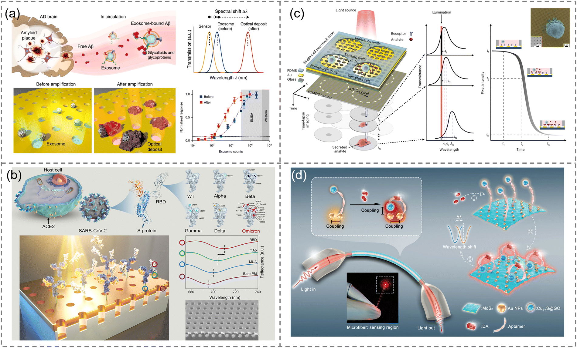 | ||
| Fig. 29 RI sensing for molecular detection. (a) APEX platform for analysis of circulating exosome-bound Aβ. When exosomes localize on the nanopore, they change the refractive index near the nanopore, resulting in a red shift in the plasmon resonance frequency. Adapted with permission from ref. 395, Copyright 2019 Springer Nature. (b) mAb-functionalized plasmonic nanopores for detection of SARS-CoV-2 RBD variants. Adapted with permission from ref. 396, Copyright 2023 American Chemical Society. (c) Plasmonic nanopore arrays for spatiotemporal mapping of single-cell secretion. Adapted with permission from ref. 397, Copyright 2023 Springer Nature. (d) Plasmonic coupled optical microfiber biosensor for DA detection. Adapted with permission from ref. 398, Copyright 2023 Wiley. | ||
Plasmonic RI sensors can also be used for early diagnosis of infectious diseases.399 In recent years, the global pandemic of COVID-19 has posed a huge health threat to the world.400 This is despite tremendous efforts in vaccination, prevention and treatment.401 However, shortages of health care resources pose huge challenges to low- and middle-income countries.402 Therefore, the development of rapid, reliable testing tools remains critical to containing current and future outbreaks of SARS-CoV-2 variants and reducing hospitalization and mortality in older patients.403,404 To date, a variety of devices based on antigen and antibody immunoassays have been studied for the detection of the COVID-19 virus.405,406 Among them, plasmonic RI sensors have received widespread attention due to their label-free and real-time detection characteristics. Recently, some researchers have developed COVID-19 detection platforms based on plasmonic RI sensing technology.407–409 For example, Funari et al. developed a gold nanospike optical microfluidic sensing platform based on the principle of LSPR for detecting COVID-19 spike protein antibodies in plasmon.410 Due to biomolecule binding events (i.e., antigen–antibody binding), the RI changes around the metal structure, resulting in a red shift of the LSPR peak. Quantitative detection of COVID-19 is achieved by monitoring the red shift of the LSPR peak, with a detection limit of 0.5 pM for this sensing platform. Furthermore, Li et al. developed a label-free plasmonic nanopore sensor functionalized with monoclonal antibodies (mAbs) and demonstrated its binding characteristics with 12 SARS-CoV-2 spike receptor-binding domain (RBD) variants (Fig. 29b).396 This plasmonic nanopore exhibits four vibrational modes. The binding kinetics between the 12 SARS-CoV-2 RBD variants and the mAb-functionalized plasmonic nanopores were experimentally recorded. The study shows that the fabricated plasmonic nanopores can effectively differentiate the SARS-CoV-2 Omicron BA.2 variant from other respiratory viruses. The detection limit is significantly lower than that of mainstream commercial kits, and it exhibits ultra-sensitive detection performance in both saliva and serum samples. Not only that, plasmonic RI sensors are also used for other virus detection.411–413
Compact and cost-effective optical devices for highly sensitive trace molecule detection are of great interest in many applications. However, when the amount of attached species is very small, highly sensitive and high-resolution spectrometers are required to record the tiny spectral shifts caused by the analyte. Such spectrometers are often bulky, expensive, and complex, which hinders the application of metasurfaces in molecular sensing and many other everyday detection scenarios. Molecular detection based on spatial multiplexing imaging has recently been developed to overcome the above difficulties.414,415 Due to structure-dependent light scattering properties, properly designed spatially varying nanostructures have position-dependent reflectance or transmittance under narrowband light illumination and therefore exhibit intensity patterns. Adsorption or attachment of analyte molecules to the metasurface changes the intensity pattern, and changes in the intensity pattern can be captured by a camera.378 This novel sensing method greatly simplifies the measurement equipment and demonstrates impressive sensitivity. Currently, pixelated metasurfaces (discrete changes in the geometry of nanostructured building blocks) and gradient metasurfaces (continuous changes in geometry) have been demonstrated.288,416 In addition, this method can also be used for high-throughput parallel real-time spatial and temporal monitoring of cellular exosomes in hundreds of single cells. For example, Ansaryan et al. proposed a label-free nanoplasmonic imaging system capable of spatiotemporally mapping single-cell secretions in a microwell array format (Fig. 29c).397 Gold nanohole arrays are used to support plasmon resonances. A complementary metal oxide camera is used to record spectral changes in surface plasmon resonances caused by analyte binding to receptors. The system can record intensity images of a large area in real time and simultaneously monitor the morphology and movement of hundreds of single cells through machine learning algorithms.
Optical fibers are also effective biosensing technology in early medical diagnosis. Optical fiber technology is known to be cost-effective, flexible, compact, immune to electromagnetic interference, and suitable for remote operations.417 However, the relatively low sensitivity severely limits the applications of optical fibers. LSPR in metal nanostructures has been proven in many works to effectively enhance the evanescent field on the surface of optical fibers, thereby improving the sensitivity of optical fiber biosensors.418–420 Currently, plasmonic optical microfiber biosensors have been demonstrated for single-molecule detection of biomarkers or single-particle sensing with a size of 48–500 nm.421,422 Subsequently, Huang et al. developed a dual-amplification nanointerface based on plasmonic coupling and conformational aptamer transition to further extend optical fiber single-molecule detection to the range of small molecules (such as dopamine (DA)) (Fig. 29d).398 Due to the dual amplification enhancement effect, the sensor can detect single-molecule level DA molecules in biologically complex samples such as cerebrospinal fluid, whole serum, and artificial sweat, with detection limits of 1.30 am, 1.53 am, and 0.54 am, respectively. Furthermore, replacement by appropriate aptamers allows the sensor to be used to detect other target small molecules and ions at the single-molecule level.423–426
 | (8) |
In 1980, Hartstein et al. first discovered the SEIRA phenomenon through metal island films.4 However, the randomness and non-resonant enhancement mechanism of metal island films lead to smaller EF (usually 101–102).38,432 The emergence of metasurfaces brings new opportunities for the development of SEIRA technology.433–437 The metasurface with a periodic structure not only overcomes the difference in randomness of the metal island film, but can also enhance its resonance by customizing the structure. In recent years, with the rapid development of micro-nano processing technology, various attractive structures have been proposed and prepared, such as asymmetric cross structures,339,438 split resonant rings,439 and fractal geometry.440,441 The diverse structures provide unique opportunities to flexibly manipulate electromagnetic waves and improve SEIRA performance. These diverse structures are mostly based on artificial design. However, due to human beings' limited ability to think in extra dimensions, the structural design of metasurfaces tends to be simple geometric figures.442 In addition, manual parameter optimization often consumes a lot of time and human resources. The rise of machine learning provides new solutions for reverse engineering metasurfaces.443–447 The introduction of machine learning and other artificial intelligence technologies not only shortens the design cycle of metasurfaces, but is also expected to unlock new optical effects.448,449
Improving sensitivity is one of the important themes in SEIRA technology. Extensive research has shown that maximum SEIRA sensitivity is achieved when the plasmon resonance frequency matches the molecular vibration frequency.450–453 In addition, increasing the near-field intensity is also the main way to improve SEIRA sensitivity.454 A commonly used method to improve near-field strength is to prepare small gaps, including horizontal gaps280,298,455 and vertical gaps.456–460 For example, Dong et al. prepared a plasmonic bowtie nanoantenna with a horizontal gap of less than 3 nm,455 and obtained a theoretical SEIRA EF of 107. Studies have shown that nanoscale gaps allow the sensing platform to detect as few as 500 4-nitrophenol molecules. On the vertical gap, using micro/nano flow channels to deliver analytes close to the antenna is an effective solution. However, as microfluidics decreases to nanometer scales, delivering analyte molecules into these gaps (i.e., hot spots) becomes increasingly difficult, especially when the gap dimensions are comparable to the typical dimensions of the molecules. To this end, Miao et al. developed a patch-type SEIRA sensor using liquid metal.460 This method uses liquid metal to immobilize the analyte between a plasmonic nanoantenna and the liquid metal. The height of the vertical nanogap here is close to the thickness of the analyte, which can produce a huge field enhancement, thereby significantly improving SEIRA sensitivity.
In addition to near-field enhancement, improving the spatial overlap rate between molecules and near-field (hot spots) is also critical to SEIRA sensitivity. However, part of the near-field enhancement of the nanoantenna will enter the dielectric layer, preventing the molecules from fully overlapping with the hot spots. To solve this problem, a method of etching the dielectric layer to prepare nanopedestals was proposed.461–463 This approach exposes hot spots to free space to increase the spatial overlap of molecules with the near field. Compared with nanoantennas on substrates, the SEIRA sensitivity of nanopedestals can be increased by 2.5–10 times.462 In addition, the passive capture of molecules by the nanopedestal further enhances the sensitivity of SEIRA.464 Coating the surface of plasmonic nanoantennas with molecule-enriched films or modifying probe molecules is another way to improve the spatial overlap of molecules and hot spots. Molecular enrichment films have proven effective for detecting discrete gas molecules.465–471 For example, Zhou et al. used ZIF-8 as a molecular enrichment film to improve the detection sensitivity of gas molecules.472 Subsequently, Zhou et al. used metal–organic framework (MOF)/polymer hybrid films to reduce the detection limit of CO2 gas molecules to sub-ppm levels (Fig. 30a).473 Probe molecules are often used to specifically adsorb proteins, nucleic acids, and lipids in a liquid environment.278–280,427,474–476 Under the action of probe molecules, SEIRA technology can achieve dynamic detection of low-concentration biomolecules. Recently, new methods for improving sensitivity have emerged, such as loss optimization54,457,477 and complex frequency wave synthesis.478
 | ||
| Fig. 30 SEIRA for molecular detection. (a) MOF/polymer-integrated multi-hotspot mid-infrared nanoantennas for sensitive detection of CO2 gas. (I) Schematic diagram of the sensing platform. (II) Schematic showing the capture of CO2 gas molecules by the porous MOF-PEI hybrid film. (III) LOD of the hybrid platform for CO2 gas detection. Adapted with permission from ref. 473, Copyright 2022 Springer Nature. (b) Customized OC resonators for ultra-broadband and ultra-sensitive molecular detection. (I) Calculated sensitivity of plasmonic nanoantennas based on coupled-mode theory. (II) Absorption spectra and absorption difference spectra of plasmonic nanoantennas with different coupling modes after loading molecules. Adapted with permission from ref. 479, Copyright 2024 Springer Nature. (c) AI-enhanced “photonic nose” for mid-infrared spectroscopic analysis of trace VOC mixtures. (I) Schematic diagram and transmission spectrum of plasmonic nanoantennas. (II) Schematic diagram of the working mechanism of “Photonic Nose”. (III) and (IV) Classification and regression models of machine learning. Adapted with permission from ref. 6, Copyright 2024 Wiley. | ||
Improving bandwidth is another theme in SEIRA technology. Broadband spectroscopy can collect more fingerprint information, thereby enabling precise identification of molecules and fingerprint retrieval. Currently, a variety of structures have been developed for constructing broadband/multiband plasmon resonances, including fractal geometry,440,441,480 self-similar structures,481,482 asymmetric structures,339 gradient metasurfaces,483,484 and supercells.485 Placing multiple nanoantenna structures supporting different frequencies within a single unit cell is a common method to achieve broadband/multiband.486 However, as the density of antennas within the unit cell increases, the coupling between adjacent antennas also gradually increases. Supercells are an effective strategy to weaken the coupling of adjacent nanoantennas.485 The supercell is composed of 16 sub-unit cells, and each sub-unit cell contains a hook-shaped nanoantenna. A broadband spectrum covering 6–9 μm is obtained by gradually changing the size of the nanoantenna. Splicing discrete spectra into continuous spectra is also a strategy to achieve broadband.355,487–489 A typical advantage of this strategy is to establish a one-to-one mapping relationship between spectral information and spatial positions, thereby achieving spectrometer-free detection. However, this one-to-one mapping relationship results in a device with a larger area. To obtain a broadband spectrum in a smaller footprint, Li et al. designed an OC metamaterial absorber based on coupled mode theory.348 This absorber has a broadband enhancement effect, and its enhancement bandwidth covers 6–14 μm. Benefiting from the broadband enhancement properties, Li et al. used a single array to achieve fingerprint retrieval for 13 analytes for the first time. Despite the large bandwidth of the OC metamaterial absorber, its sensitivity is relatively low. To achieve both broadband and high sensitivity in a metamaterial absorber, Li et al. introduced a plasmon-molecule coupling channel into the OC device (Fig. 30b).479 The plasmon-molecule coupling channel can be modulated by adjusting the gap between adjacent nanoantennas. By reducing the gap between the nanoantennas, Li et al. developed a device with both bandwidth and sensitivity surpassing previous designs. Specifically, the sensitivity of the device reached 7.25% nm−1.
The introduction of machine learning has further promoted the rapid development of SEIRA technology.128,129,348,485,490,491 For example, Kavungal et al. developed an immunoassay-coupled nanoplasmonic infrared metasurface sensor for the specific detection of proteins associated with neurodegenerative diseases.492 Aided by an artificial neural network, the sensor achieves unprecedented quantitative predictions of mixtures of oligomers and fibrin aggregates. SEIRA technology provides a valuable toolkit for studying dynamic reactions between molecules. However, infrared spectroscopy presents challenges in separating overlapping vibrational modes. Zhou et al. used stacked infrared nanoantennas to excite the coupling modes of localized surface plasmons and SPhP to solve the problem of overlapping vibration modes.47 The research results have shown that SPhP vibration in the Reststrahlen band is particularly sensitive to molecular RI. Owing to the strong dependence of SPhP on RI, combined with deep neural network algorithms, the strongly overlapping molecular vibrations in biological reactions are dynamically unraveled. In gas sensing, Xie et al. introduced an artificial intelligence (AI)-enhanced “photonic nose” for trace-level volatile organic compound (VOC) gas analysis in the mid-infrared spectrum (Fig. 30c).6 The MOF-coated plasmonic nanoantenna is designed to target VOC molecular fingerprints, achieving detection limits in the single-digit ppm range for isopropyl alcohol, ethanol, and acetone. Given the overlapping absorbance peaks among VOCs, deep learning models were employed. A convolutional neural network (CNN) model classified 125 VOC mixtures with 100% accuracy. A multilayer perceptron (MLP) model then decomposed the spectra into pure components, enabling accurate concentration predictions within an error of 10 ppm even in the presence of interferences.
 | (9) |
| EFSERS = EF(ωest)·EF(ωdet) | (10) |
SERS has received increasing attention in recent years due to its ultra-high sensitivity and selectivity in detecting extremely low concentrations of molecules. Currently, the development of SERS theory, SERS substrates, and related instruments has promoted its diverse applications in biomedical detection, nanomaterial characterization, food science, and environmental analysis.35,500,501
Surfaces and interfaces play crucial roles in many disciplines, including heterogeneous catalysis, electrochemistry, and photo(electro)chemistry.502 To fully understand surface and interfacial processes, it is necessary to obtain molecular-level information from surfaces and surface-interacting molecules. The SERS method is a powerful technique for studying surfaces and interfaces due to its ultrahigh surface sensitivity.503 For example, Yu et al. developed a depth-sensitive plasmon-enhanced Raman spectroscopy method to detect the nanostructure and chemical properties of the solid electrolyte interface (SEI) on lithium anodes.504 Dynamic molecular-level information provided by plasmon-enhanced Raman spectroscopy reveals the formation and evolution of the SEI in lithium metal batteries. The research results are of great significance to further guide the SEI design of lithium metal batteries and improve SEI performance. With its high spatial resolution and ultra-small nanogaps, SERS can also be used for nanoscale chemical analysis of heterogeneous surfaces and to study single molecule optomechanics.505–507
The rich fingerprint vibration information obtained based on SERS provides a unique opportunity to develop photonic noses and photonic tongues. Inspired by the nose, Kim et al. proposed a SERS functionalized array to realize a powerful artificial nose sensing platform.508 Eight SERS substrates were modified with differently functionalized SAMs. Multiple functionalized SERS substrates can embrace complex spectral information, thereby greatly improving the accuracy of biological sample identification in the absence of target-specific binding receptors. Based on a similar sensing strategy, Leong et al. demonstrated a SERS-based breath analyzer for rapid and non-invasive screening of individuals for COVID-19, achieving 96.2% sensitivity and 99.9% specificity. Due to the advantage that SERS technology can work in a liquid-phase environment, it also provides opportunities for the development of photonic tongues. Ling and colleagues proposed a SERS taster for multiplex analysis of wine flavor.509 The taster captures chemical functionality within flavor molecules by employing many non-covalently interacting receptors. Ling et al. constructed comprehensive “SERS superprofiles” by combining the SERS spectra of all receptor flavors for predictive analytics using chemometrics.
There is great potential to conduct biomolecular testing directly at the point of care in a non-invasive manner.510 However, there is a mismatch between traditional rigid SERS sensors and soft elastic organisms, which greatly limits their application in the wearable field. In this context, the development of flexible wearable SERS substrates has attracted great interest. In a recent example, Wang et al. proposed a wearable plasmonic metasurface sensor for non-invasive universal molecular fingerprint detection at biological interfaces (Fig. 31a).511 This integrated platform is achieved by integrating a flexible SERS-active plasmonic metasurface as a key sensing component and a flexible electronic system capable of automatically extracting sweat and analytes from the body. Since each molecule has a unique SERS spectrum, the sensor can “fingerprint” targets extracted from sweat. Subsequently, Mogera et al. demonstrated a wearable microfluidic system based on plasmonic paper for continuous and simultaneous quantitative analysis of sweat loss, sweat rate, and metabolites in sweat.512 An integrated flexible plasmonic wearable sensor is capable of sensitive detection and quantification of uric acid in sweat at concentrations as low as 1 μM. In the future, integrated flexible SERS sensors will show great potential in human health assessment, personalized diagnosis and treatment, and drug delivery.513
 | ||
| Fig. 31 SERS for molecular detection. (a) Plasmonic metamaterial-integrated wearable SERS sensing device. (I) Schematic drawing showing the working principle and design of the device. (II) Schematic illustration showing the SERS sensing principle of the nanocube metafilm. (III) SERS spectra of the human sweat samples. Adapted with permission from ref. 511, Copyright 2021 AAAS. (b) SERS nanosensor for the real-time monitoring of multiple stress signalling molecules in plants. (I) Schematic diagram of the synthesis of SERS-active nanoparticles. (II) Schematic of the enhanced Raman scattering on the surface of silver nanoshells. (III) Schematic diagram of early diagnosis of fungal diseases in crops based on SERS. (IV) Monitored SERS spectra of fungal infections in wheat. Adapted with permission from ref. 514, Copyright 2022 Springer Nature. | ||
In addition to human health monitoring, SERS technology can also be used for plant health monitoring.515,516 Monitoring plant health can increase plant productivity, optimize resource allocation of water and agrochemicals, and select optimal plant traits. Under stress conditions, plants release endogenous chemicals that trigger their defense mechanisms. Therefore, monitoring these endogenous signals can serve as a reliable indicator of plant health. Common endogenous signals encompass salicylic acid (SA), extracellular adenosine triphosphate (eATP), phytoalexins, and glutathione. Several studies have utilized SERS probes for detecting endogenous biomolecules or pathogens in plant extracts or isolated leaves.517–520 Notably, a recent study by Son et al. presented an innovative approach for non-destructive detection of signaling molecules within living plants (Fig. 31b).514 They introduced SERS nanoprobes into the intercellular space to monitor the transport of signaling molecules in the apoplast. These SERS nanoprobe applications successfully identified SA, eATP, cruciferous phytoalexins, and glutathione in nasturtium, common wheat, and barley under various stressors, both biotic and abiotic. Furthermore, SERS technology has found utility in detecting pesticide residues,521,522 banned food additives,523,524 and mycotoxins in agricultural products.525,526 This multifaceted application of SERS underscores its potential as a versatile tool in agricultural monitoring and management.
However, the intramolecular CD signal intensity is very small, usually around the 10−5 level. To address this limitation, leveraging chiral plasmonic structures has emerged as a promising solution.530 In 2010, Kadodwala and colleagues pioneered the utilization of plasmonic planar chiral metamaterials for detecting chirality across various proteins (Fig. 32a).531 Their method capitalizes on metallic gamma ion arrays on substrates, which can exist in left- or right-handed configurations. Each type of array converts incident linearly polarized light into elliptically polarized light with consistent chirality. Upon biomolecule adsorption, these metal gamma ion arrays induce resonance shifts due to the high sensitivity of surface plasmon modes to the refractive index of their surroundings. Notably, the refractive index of chiral molecules differs under left-handed and right-handed circularly polarized light, potentially leading to distinct resonance shifts in the plasmon. Thus, detecting chiral molecules involves measuring disparities in resonance shifts. Studies indicate that plasmons can enhance chiral sensitivity by up to six orders of magnitude compared to conventional CD measurements. Subsequently, the same research group introduced a shuriken-shaped metasurface, which facilitated the detection of viruses,532 antibodies,533 and peptide molecules.534 This advancement leveraged enhanced chiral asymmetry and subwavelength spatial localization, further broadening the scope of chiral molecule detection in diverse applications.
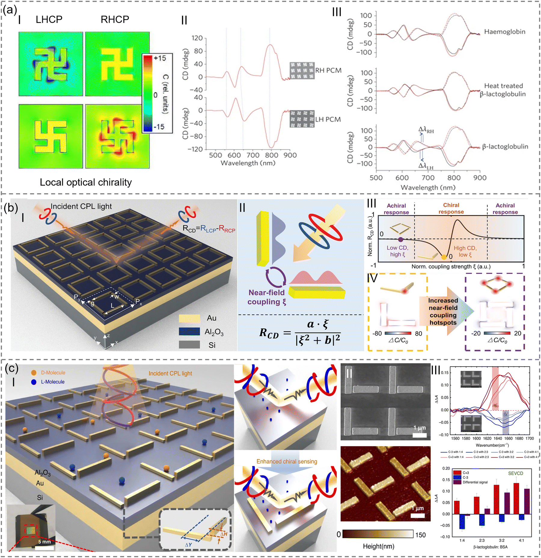 | ||
| Fig. 32 Surface plasmon-enhanced chiral spectroscopy for molecular detection. (a) Ultrasensitive detection and characterization of biomolecules using superchiral fields. (I) Local optical chirality. (II) CD spectra collected from LH/RH planar chiral metamaterials immersed in distilled water. (III) Influence of the adsorbed proteins on the CD spectra of planar chiral metamaterials. Adapted with permission from ref. 531, Copyright 2010 Springer Nature. (b) Near-field induced less chiral response for chiral molecular sensors. (I) Schematic drawing of the chiral metamaterials. (II) Schematic illustration of the near-field coupling between perpendicularly positioned plasmonic resonators. (III) Calculated RCD as a function of coupling strength. (IV) Simulation of the optical chiral field for both double-resonator and quadruple-resonator structures. Adapted with permission from ref. 535, Copyright 2023 Wiley. (c) Expanding chiral metamaterials for retrieving fingerprints via vibrational circular dichroism. (I) Schematic drawing of the surface enhanced VCD sensing platform. (II) Device characterization. (III) Experimental demonstration of chiral mixture sensing. Adapted with permission from ref. 536, Copyright 2023 Springer Nature. | ||
Currently, commonly used CD spectra are situated in the UV, visible, and near-infrared regions, primarily because the stronger CD signals of molecules are found at shorter wavelengths. However, CD signals at these wavelengths often fail to provide detailed information about the chemical structure of the molecule, which limits their utility in distinguishing various types of chiral molecules within mixtures. In recent years, there has been a push to extend the CD spectrum into the mid-infrared region to acquire vibrational circular dichroism (VCD).537 Unlike CD spectra, VCD offers more comprehensive molecular structure information by exploiting vibrational transitions of chiral molecules. Nonetheless, the longer wavelength VCD signal is typically 2 to 3 orders of magnitude smaller in intensity than the CD signal.538,539 Plasmonic systems present a potential avenue for enhancing VCD signals. For instance, Chanda's team utilized an achiral plasmonic system to boost VCD detection sensitivity by 4 orders of magnitude.540 More recently, the same team significantly enhanced the detection sensitivity of chiral molecules by fine-tuning an achiral plasmon system. Experimental findings illustrate that compared to traditional VCD spectroscopy technology, the plasmon system can elevate the detection sensitivity of chiral molecules by up to 13 orders of magnitude.541 While numerous research efforts have demonstrated that chiral structures can amplify VCD signals, the underlying mechanism remains unclear. Addressing this, Xu et al. embarked on a study beginning with the fundamental relationship between planar chiral metamaterials and chiral response (Fig. 32b).535 They theoretically hypothesized that near-field coupling strength might be a pivotal factor in far-field CD. To test this hypothesis, Xu et al. devised a selective exposure method to cover the nanogap of the four-resonance metamaterial, probing the correlation between the near-field coupling coefficient and the far-field CD response. Experimental results ascertain that enhanced chiral near-field plays a pivotal role in amplifying molecular signals. This critical finding paves the way for achieving ultra-small volume and label-free detection of chiral molecules. Given that the VCD spectrum contains information pertaining to the vibration of chiral molecules, it offers the feasibility of distinguishing the identity and chirality of enantiomers. Leveraging this characteristic, Xu et al. proposed an enhanced VCD sensing platform based on plasmonic chiral metamaterials for discerning the secondary structures of different proteins (Fig. 32c).536 In this endeavor, Xu and colleagues demonstrate, for the first time, the potential of utilizing surface-enhanced VCD to detect chiral mixtures, thereby broadening the scope of VCD spectroscopy.
In recent years, Raman optical activity (ROA) has emerged as another valuable chiral spectroscopy technique.542 One of its primary advantages lies in its capability to analyze water dispersion samples, which may be too absorbent for VCD.543 However, conventional ROA also faces the challenge of low signal intensity. Addressing these inherent limitations of ROA can be achieved through surface plasmon enhancement techniques. In 1983, Efrima first proposed the feasibility of surface-enhanced ROA spectroscopy in the literature.544 Subsequently, Efrima introduced a theoretical treatment method for surface-enhanced ROA.545 Building upon this theoretical foundation, Janesko and colleagues put forward an electromagnetic enhancement model tailored for surface-enhanced ROA spectra.546 This model offers a concise framework that integrates the fundamental equations for unenhanced ROA with modifications to the molecular response tensor induced by substrate's electromagnetic enhancement. Presently, this model stands as the most widely adopted theoretical formulation in surface-enhanced ROA. On the experimental front, Sun and colleagues developed advanced optical technologies to detect ROA signals of molecular structures.547 They augmented Raman signal intensity by utilizing silver chiral nanowires as plasmonic waveguides. This technique allows for the differentiation of Raman spectra excited by left- and right-handed circularly polarized light, facilitating the determination of sample chirality and conformation. Additionally, Ostovar and his team uncovered a novel chiral transfer mechanism to enable surface-enhanced ROA.548 This mechanism stems from the breaking of inversion symmetry in achiral nanoparticles when interacting with nearby chiral molecules, subsequently altering the symmetry of the excitation fields of left-handed circular polarization (LCP) and right-handed circular polarization (RCP). Such alterations in circularly polarized light symmetry result in asymmetric absorption in achiral probes, detectable through Raman spectroscopy.
The prospect of extending CD spectroscopy into the terahertz range is intriguing due to the ability of THz spectroscopy to capture both vibrational and rotational information of biological macromolecules. This has spurred considerable interest in realizing terahertz circular dichroism (TCD).549 However, the absence of polarization modulation in terahertz radiation has hindered the widespread adoption of TCD. Recently, the use of nonlinear metasurfaces to generate terahertz waves with different circular polarizations has presented new opportunities for achieving TCD. For instance, Choi et al. employed periodic kirigami cutting to transform plasmonic sheets into tunable optical elements, enabling polarization modulation of THz radiation.550 The herringbone pattern of microscopic metal strips facilitated a dynamic polarization rotation modulation range of over 80° across thousands of cycles. The advent of polarization modulators has paved the way for realizing TCD spectra. Subsequently, McDonnell and colleagues introduced a broadband terahertz emitter based on the Pancharatnam–Berry phase nonlinear metasurface, which exhibits unique optical functionalities.551 Through the Pancharatnam–Berry phase nonlinear metasurface, both the polarization and phase of the terahertz wave can be precisely controlled. McDonnell et al. further showcased the application of PB-phase nonlinear metasurface emitters in TCD spectroscopy. TCD spectroscopy offers a distinctive tool for detecting chiral phonons in various biomolecule crystals.552 The identification of chiral phonons not only facilitates a deeper understanding of biochemical processes but also unlocks new avenues for medical applications of terahertz photonics.553
SEF spectroscopy stands out as a remarkable tool offering ultra-high sensitivity for detection and imaging down to the single-molecule level. In the 1960s, Drexhage and colleagues made the initial observation that the decay time of molecular fluorescence correlates with the distance between the excited molecule and the metal film.555 Subsequently, extensive research on this phenomenon has been conducted by groups led by Lakowicz and Geddes.556–561 Early implementations of SEF commonly utilized rough silver island films as substrates.562–564 In recent years, with advancements in nanoparticle synthesis technology, noble metal nanoparticles with diverse morphologies have gained prominence as SEF substrates.565–568 In 2006, Kühn et al. demonstrated a notable advancement by employing scanning probe technology to couple a single molecule to a single spherical gold nanoparticle functioning as a nanoantenna, resulting in a fluorescence enhancement of over 20 times.569 Nonetheless, gold nanospheres lack preferential dipole directions, and the probe does not support any resonant coupling modes, leading to limited fluorescence enhancement effects.570 To address this limitation, the utilization of nanoshells, nanorods, nanopores, and nanobowties has been proposed to enhance local fluorescence.571–575 Notably, Kinkhabwala and colleagues utilized electron beam lithography to fabricate gold bowties reduced to 14 nm (Fig. 33a).571 The nanogap in these structures provides substantial field enhancement, achieving an impressive fluorescence enhancement of up to 1340-fold. This groundbreaking work significantly advances the application of SEF in small molecule detection, heralding new possibilities in the field.
 | ||
| Fig. 33 SEF spectroscopy for molecular detection. (a) Large single-molecule fluorescence enhancements produced by a bowtie nanoantenna. (I) Scanning electron microscopy (SEM) image of a gold bowtie nanoantenna. (II) Finite-difference time-domain calculation of local intensity enhancement. (III) Scatter plot of fluorescence brightness enhancement of 129 fluorescent molecules as a function of bowtie gap size. Adapted with permission from ref. 571, Copyright 2009 Springer Nature. (b) Real-time detection of single-molecule reaction by plasmon-enhanced spectroscopy. (I) Schematic diagram of plasmon-enhanced single-molecule spectroscopy. (II) Simulation of the electric field distribution. (III) The characteristic emission intensity trace of a single rhodamine B isothiocyanate molecule, exhibiting blinking behavior and single-step photobleaching events. Adapted with permission from ref. 576, Copyright 2020 AAAS. (c) Light-enhancing plasmonic-nanopore biosensor for DNA detection. (I) Schematic diagram of the plasmonic nanopore device. (II) Detection signal of the non-plasmonic device. (III) Detection signal of the plasmonic nanopore device. Adapted with permission from ref. 577, Copyright 2016 Wiley. | ||
Single molecule detection represents a pivotal application area within the realm of SEF spectroscopy.578–580 In 2007, Lakowicz et al. achieved a significant milestone by detecting the fluorescence signal of rhodamine on a silver island membrane substrate.581 Fluorescence emission from rhodamine increased 7-fold and the fluorescence lifetime was shortened using silver island films as substrates. Subsequently, Orrit et al. employed wet chemistry to synthesize a large quantity of AuNRs, providing fluorescence enhancement comparable to photolithographic components.575 Experimental findings revealed that AuNRs yielded over 1000-fold fluorescence enhancement for nearby crystal violet molecules, with a quantum yield of 2%. More recently, there have been reports employing SEF to detect antibiotic molecules.582–586 Beyond single molecule detection, there's significant interest in utilizing SEF to monitor reactions involving individual molecules.587 The study of single-molecule reactions serves to deepen our understanding of chemical processes.588,589 For instance, Li et al. utilized a plasmonic nanocavity substrate to enhance the fluorescence and Raman signals of single molecules (Fig. 33b).576 Conformational transitions and removal of the carboxyphenyl group within the molecule induced shifts in the fluorescence emission band. Raman signals were utilized to identify reaction intermediates and unveil underlying reaction mechanisms. By correlating fluorescence spectra with Raman signatures, Li et al. achieved real-time monitoring of the light-induced cleavage reaction of individual rhodamine B isothiocyanate molecules.
Nucleic acids, such as DNA, are among the most important molecules in living organisms, as they carry and transmit genetic information that determines biological traits.590 Therefore, accurate detection of nucleic acid molecules is crucial. Plasmonic nanopores have become one of the key tools for nucleic acid detection.591 There are two main advantages to using plasmonic nanopores for nucleic acid detection. First, the potential gradient near the nanopore actively guides the nucleic acid molecules into the pore region.592 Compared to passive diffusion, this active transport enables single-molecule detection even at low concentrations. Second, the typical nanopore diameter is designed to be slightly larger than the cross-section of the nucleic acid molecule, which restricts the movement of the molecule to a single dimension while ensuring continuous occupation of the sensing volume.591 This restriction allows for single-molecule detection across a wide range of concentrations by increasing the residence time of the molecule. Additionally, as nucleic acid molecules pass through the nanopore, their polymer chains can be linearized, enabling continuous observation of submolecular sequences. For example, Assad et al. proposed a plasmon nanopore-based device for detecting individual DNA molecules (Fig. 33c).577 In this device, a SiNx membrane faces the analyte source and the nanopore acts as a physical gate. This approach allows only one molecule to enter the nanopore at a time, reducing background noise. To characterize the sensing properties of the plasmonic nanopore, Assad et al. covalently labeled a 5 kbp double-stranded DNA with the fluorophore CF640R. Each DNA molecule contained seven fluorophores and was introduced into the cis chamber at a relatively low concentration of 0.1 nM or less. The study showed that the peak fluorescence intensity increased more than tenfold as the DNA molecule passed through the plasmonic nanopore compared to non-plasmonic devices.
Detection of amino acids and proteins using SEF holds significant promise, especially considering the crucial role amino acids play as the fundamental building blocks of various proteins in the human body. Such detection aids in early risk assessment of chronic and malignant diseases. Lakowicz et al. proposed a fluorescence-enhancing substrate based on aluminum nanoparticles for label-free detection of amino acid molecules.582 Their work demonstrated a remarkable 3500-fold fluorescence enhancement when the fluorophores were oriented perpendicular to the aluminum surface. Additionally, Lakowicz et al. showcased the fluorescence enhancement of tryptophan and tyrosine by aluminum nanoparticles. The pioneering work by Geddes and colleagues marked the first instance of protein detection using SEF.593 Since then, SEF has been employed to detect various protein molecules, including erythrin, algal proteins, and recombinant proteins. In recent years, the utilization of aptamer sensors has gained popularity. Aptamers, functional single-stranded DNA or RNA molecules (10–100 nucleotides), offer unique sensitivity and specificity in binding to a variety of target molecules, such as small molecules, viruses, proteins, peptides, and even cells. Chen et al. proposed a novel fluorescent polarization aptasensor based on bivalent aptamers and silver nanoparticles for lactoferrin detection.594 The bivalent aptamer was engineered to attach to the signaling molecule fluorescein isothiocyanate and the enhancer silver nanoparticles. By incorporating second-order aptamers, the distance between silver nanoparticles and fluorescent dyes could be minimized. Experimental results demonstrated that the detection sensitivity of this sensor is approximately 3 orders of magnitude higher than that of traditional aptamer-based homogeneous detection, with a detection limit of 1.25 pM. These advancements in SEF-based detection methods hold immense potential for early disease diagnosis and biomedical research, offering enhanced sensitivity and specificity in detecting amino acids and proteins.
The utilization of SEF for detecting bacteria and viruses is of utmost importance, especially in the context of public health and disease management. The pioneering work in SEF-based bacterial detection was conducted by the Lakhtakia team.595 They employed porous metal-engraved films comprising silver, aluminum, gold, and copper as substrates to detect E. coli in water. Experimental findings revealed that the device exhibited approximately 20 times fluorescence enhancement compared to traditional glass substrates. Subsequently, Huang et al. also contributed to the detection of E. coli using SEF.596 They utilized mixed thiol SAMs of PEG-thiol and COOH-thiol modified gold surfaces as substrates and leveraged long-range surface plasmons to enhance fluorescence spectroscopy. Their experimental results indicated a detection limit below 10 CFU ml−1, with analyte concentrations ranging from 10 to 106 CFU ml−1. In recent years, with the emergence of the global COVID-19 pandemic, the urgency for various sensing methods to facilitate virus detection has become paramount. Addressing this need, Hu et al. employed nanostructured plasmonic gold chips for multiplex assessment of antibodies against various virus variants.597 Experimental results demonstrated that the detection limit of these chips was as low as 20 fM, more than two orders of magnitude lower than that of glass substrates. Subsequently, Zhu et al. introduced an in-frame gold particle nanostructure for direct assessment of the SARS-CoV-2 nucleocapsid protein.598 By integrating gold nanostructures with a microplate reader, the sensor achieved a sensitivity of 44 fg mL−1 in just 3 minutes. To further enhance analytical sensitivity, Zhu et al. employed single-molecule counting technology, achieving a detection limit as low as 0.84 ag mL−1. These advancements highlight the potential of SEF-based techniques in achieving rapid and sensitive detection of bacteria and viruses, thus playing a crucial role in disease surveillance and management efforts.
Beyond nanospectroscopy, PIRET also plays a significant role in molecular imaging. While fluorescence imaging has demonstrated exceptional performance in biological applications, it lacks chemical fingerprint information. Moreover, the broad absorption and emission spectra of organic fluorophores, along with their susceptibility to photobleaching and blinking effects, limit their effectiveness in long-term imaging and multiplexing.602 In contrast, plasmonic nanoparticles based on PIRET offer a promising solution for hyperspectral imaging.603 For example, Kim et al. developed a PIRET-based metasurface-driven multiplexed nanospectroscopy platform for real-time monitoring of multiple biomolecules within live cells.604 Compared to traditional fluorescence and chemiluminescence methods, this platform leverages the stability of molecular absorption signals to overcome the constraints of photobleaching and complex preprocessing. The metasurface in their study was composed of aggregated aluminum nanodisks, which selectively modulated the scattering spectrum across the entire visible range, enabling simultaneous detection of different biomolecules. When the scattering peak of the metasurface matched the absorption frequency of a specific biomolecule, strong PIRET occurred, leading to quenching in the scattering spectrum. This approach facilitated high-spatial-resolution molecular imaging, advancing molecular sensing technologies.
4.3. Multi-effect fusion for molecular detection
Graphene, a single-atom-thick planar material, has unique electronic and optical properties. Importantly, the carrier density (i.e., Fermi level) of graphene can be adjusted through electrostatic gating or chemical doping, allowing precise tuning of plasmonic resonances. By patterning graphene into nanoribbons, electromagnetic waves propagating in free space can directly couple to graphene and generate local plasmons. These local plasmons can significantly enhance light–matter interactions, thereby markedly increasing molecular absorption of infrared vibrational modes. Li et al. were the first to demonstrate the application of graphene nanoribbons in enhancing polymer film vibrational sensing.315 Rodrigo et al. dynamically controlled the Fermi level of graphene nanoribbons by applying a bias voltage, achieving dynamic tuning of graphene plasmonic resonances.313 The results showed that electrically tunable graphene could enable a single device to perform SEIRA sensing across a wide spectral range, thus enhancing the detection of specific vibrational fingerprints. Using the same approach, Hu et al. designed a graphene plasmonic structure for sub-monolayer molecular detection (Fig. 34a).611 In their work, the graphene plasmonic structure was fabricated on a CaF2 substrate to eliminate the strong plasmon–phonon hybridization in the traditional graphene plasmonic structure. Using far-field Fourier transform infrared spectroscopy, the graphene plasmonic can achieve a highly selective average enhancement of up to 20 times. Subsequently, the same research group successively designed a graphene plasmonic structure for protein detection in gas and aqueous solutions.314,612
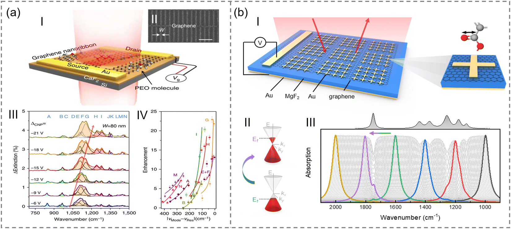 | ||
| Fig. 34 Electrically tunable plasmons for molecular detection. (a) Graphene plasmon enhanced molecular fingerprint sensor. (I) Schematic of the sensor. (II) SEM image of the graphene nanoribbon pattern. (III) Highly selective detection of molecular vibrational fingerprints. (IV) Enhancement as a function of spectral detuning. Adapted with permission from ref. 611, Copyright 2016 Springer Nature. (b) A hybrid graphene metamaterial absorber for enhanced modulation and molecular fingerprint retrieval. (I) 3D schematic view of the hybrid graphene metamaterial absorber sensing platform. (II) Schematic diagram of graphene Fermi level modulation. (III) Absorption spectra of the sensing platform after loading analytes. Adapted with permission from ref. 613, Copyright 2023 Royal Society of Chemistry. | ||
Combining graphene with metal nanostructures also allows for the tuning of plasmonic resonance frequencies. Compared to traditional designs consisting only of metal nanostructures, the introduction of graphene enables easy tuning of plasmonic resonance frequencies by altering the Fermi level. Compared to plasmonic structures made solely of graphene nanoribbons, metal nanostructures provide stronger light–matter interactions, thereby enhancing the SEIRA effect. Chen et al. theoretically designed a broadband hybrid graphene metamaterial absorber that combines the high absorbance of metal plasmons with the electrically tunable properties of graphene, useful for molecular fingerprint retrieval (Fig. 34b).613 Chen et al. optimized the sensing sensitivity of the metamaterial absorber through loss engineering. By integrating the metamaterial absorber with graphene and adjusting the Fermi level of graphene, they achieved linear modulation of the absorber's resonance frequency within the mid-infrared range. Incorporating pixelated design concepts, this hybrid resonator can serve as a potential SEIRA platform for multi-fingerprint molecular detection, quantitative analysis, and chemical identification. Experimentally, Li et al. designed a mid-infrared hybrid graphene metasurface biosensor for simultaneous quantitative detection and molecular identification of proteins.614 The device features a metamaterial absorber structure with graphene positioned between a nanoribbon and a dielectric layer. By applying a bias voltage to the graphene, they were able to finely tune the plasmonic resonance frequency (approximately 0.95 cm−1 V−1). This precise adjustment of the plasmonic resonance frequency effectively enhances weak spectral signals, distinguishing weak fingerprint signals from device background noise. The experimental results showed that fine-tuning with graphene increased the relative absorption peak value of the protein amide I band from 5.47% to 12.84% and the relative absorption peak value of the amide II band from 4.82% to 13.82%.
Recently, researchers have explored methods that combine particle capture with optical detection by introducing nano-manipulators at sensing points (such as nano-antennas or nanopoints) to capture nanoscale objects.615 Among the various nano-manipulators, electric nanotweezers have shown significant advantages, enabling real-time and repeatable manipulation of numerous particles. Dielectrophoresis (DEP) is a typical example of electric nanotweezers. The DEP force arises from differences in conductivity and dielectric constants between polarized particles and their surrounding medium. An external electric field induces net polarization at the particle–medium interface. In a spatially non-uniform field, particles are either attracted to high-field regions (positive DEP) or repelled from them (negative DEP).
Recent research has combined DEP with plasmonic sensors to concentrate molecules and enhance RI sensing. For instance, Barik et al. integrated large-area gold nanopore arrays with ITO electrodes to achieve efficient DEP molecule capture and real-time SPR detection (Fig. 35a).616 The gold nanopore arrays are used for constructing surface plasmon-enhanced refractive index sensing. When molecules bind to the surface of gold nanopores, the resonant frequency shifts to longer wavelengths. Additionally, gold nanopore arrays serve as the bottom electrode for DEP, while ITO-coated glass slides act as the top electrode. By introducing the sample solution into the gap and applying an alternating current signal between the ITO electrode and the gold nanopore array, forces are exerted on the molecules, accelerating their movement toward the sensor surface. The results indicate that DEP technology can detect bovine serum albumin molecules at concentrations as low as 1 pM.
 | ||
| Fig. 35 Electron nanotweezers-plasmonics enhanced molecular detection. (a) DEP-enhanced plasmonic sensing with gold nanohole arrays. (I, II) Schematic of the experimental setup. (III) SEM of the nanohole array. (IV) Measured spectra. Adapted with permission from ref. 616, Copyright 2014 ACS. (b) DEP nanoparticle aggregation for on-demand SERS analysis. (I) Schematic diagram of the sensing platform. (II) SEM image of the DEP-SERS chip. (III) Close-up view of a single trap using agglomeration of nanoparticles. (IV) Typical SERS spectra acquired using the DEP-SERS chip. Adapted with permission from ref. 617, Copyright 2018 ACS. (c) Infrared spectroscopy of live cells from a flowing solution using electrically biased plasmonic metasurfaces. (I) Schematic diagram of the DEP-SEIRA platform. (II) Schematic of the metasurface pixel array. (III) SEM image of the metasurface. (IV) Measurement results. Adapted with permission from ref. 618, Copyright 2020 Royal Society of Chemistry. | ||
In addition to periodic nanopore arrays, DEP can also be integrated with other plasmonic sensors for SERS619,620 and SEIRA detection.618 Salemmilani et al. reported a microfluidic chip-based SERS platform that uses DEP technology for highly localized capture and release of SERS-active nanoparticles (Fig. 35b).617 In this platform, SERS-active silver nanoparticles are used as capture targets. Under the influence of DEP, silver nanoparticles aggregate at specific locations, creating multiple optical hotspots that enhance Raman signals of analytes in the solution. To improve the reuse of the device, electrodes and flow channels are passivated to minimize nanoparticle contamination in the microchannels. The device has been shown to detect methamphetamine at physiologically relevant concentrations in saliva within 2 minutes. In the infrared range, Kelp et al. developed a DEP-SEIRA integrated microfluidic device (Fig. 35c).618 This device incorporates DEP modules, metasurfaces, and microfluidic channels. The microfluidic channels are used to transport cells in aqueous solutions, while the plasmonic metasurfaces enhance the infrared spectra of live cells. DEP is used to attract cells to the surface of the metasurface components. With DEP, the device can acquire infrared absorption spectra of cells within one minute. When DEP is turned off, the adhered cells are released under the action of fluidic forces. This method provides a flexible approach to transporting cells to sensors, offering high throughput and usability.
Non-dispersive infrared (NDIR) spectroscopy is a type of mid-infrared gas sensor that analyzes gases based on the characteristic absorption wavelengths of mid-infrared radiation caused by gas molecular vibrations. Traditional NDIR gas sensors use broadband light sources and do not have pre-filters. To analyze the concentration of target gases, a bandpass filter is usually added before the detector to remove all unwanted wavelengths from the beam, allowing only the characteristic absorption wavelengths of the gas to reach the detector. To analyze several target gases in a mixture simultaneously, multiple “bandpass filter + optical detector” pairs are implemented in the NDIR gas sensor.621,622 However, this approach significantly increases the cost, system complexity, and operating time, especially when the number of target gases is large.623,624 This challenge stems from the lack of spectral selectivity in most commercially available mid-infrared detectors. The wavelength selectivity of plasmonic metamaterials offers a solution for narrowband mid-infrared detectors. A common approach is to integrate metamaterials with thermoelectric detectors.343,347,625,626 For example, Tan et al. integrated plasmonic metamaterial absorbers on top of a pyroelectric detector to achieve infrared response at specific wavelength bands (Fig. 36a).627 The plasmonic metamaterial absorber can absorb infrared light at specific bands and convert it into heat, thus raising the temperature at the top of the pyroelectric detector. This temperature change induces charge separation within the pyroelectric material, generating a potential difference. By measuring the magnitude of this potential difference, the intensity of the specific band of infrared light can be obtained. By adjusting the design of the metamaterial, the detection wavelength or peak absorption wavelength of the integrated absorber can be tuned to cover the entire mid-infrared spectrum. Based on this principle, Tan et al. developed eight narrowband detectors responsive to different wavelength bands, with detection wavelengths matching the characteristic absorption wavelengths of eight target gases: H2S, CH4, CO2, CO, NO, CH2O, NO2, and SO2. The detection limits for common gases such as CH4, CO2, and CO were found to be 63 ppm, 2 ppm, and 11 ppm, respectively. Additionally, with the aid of mathematical models, the concentration of two target gases in a mixture could be inferred from the voltage responses of two narrowband detectors.
 | ||
| Fig. 36 Plasmonics-based photodetectors for molecular sensing. (a) NDIR multi-gas sensing via nanoantenna integrated narrowband detectors. (I) The device geometry of the narrowband detection element. (II) The joint package of the multiple pyroelectric elements with different detection wavelengths. (III) The measured absorption spectra of 8 fabricated MIM absorbers compared to the infrared absorption bands of eight target gases. Adapted with permission from ref. 627, Copyright 2020 Springer Nature. (b) Zero-bias long-wave infrared nanoantenna-mediated graphene photodetector for polarimetric and spectroscopic sensing. (I) Schematic diagram of nanoantenna-mediated graphene photodetectors. (II) SEM image. (III) Gas sensing response and recovery characteristic. (IV) Gas sensing response time. Adapted with permission from ref. 628, Copyright 2023 Wiley. | ||
Another approach involves integrating plasmonic metamaterials with low-dimensional materials, such as graphene, to realize mid-infrared photodetectors. The unique band structure and excellent transport properties of graphene offer unique opportunities for photodetectors. However, graphene's absorption rate in the infrared range is relatively low (about 2.3%), resulting in poor responsivity and sensing performance.629 Therefore, an effective structure to enhance graphene's absorption is required. Research has demonstrated that periodic nanostructures can achieve extreme light confinement, thereby increasing absorption and interaction between light and matter.630,631 Additionally, nanoantennas can serve as small metal electrodes to collect charge carriers, generating photocurrent.632,633 Many studies have used graphene-plasmonic nanostructures to fabricate mid-infrared photodetectors, enabling the measurement of optical parameters such as wavelength, intensity, polarization, and ellipticity.14,634–636 These measurements are critical for achieving highly integrated, high spatial resolution, and surface-enhanced sensors. For example, Xie et al. proposed a graphene photodetector based on nanoantennas for polarization and spectral sensing (Fig. 36b).628 Polarization sensing is achieved through artificial near-field anisotropy realized by double L-shaped nanoantennas. The device exhibited a high responsivity of 6.3 V/W at zero bias under room temperature, with a noise equivalent power as low as 1.6 nW Hz−1/2. Finally, Xie et al. used acetone as an analyte for spectral sensing, demonstrating the application of the nanoantenna-graphene photodetector in molecular detection. The results showed a detection limit of 115 ppm and a dynamic gas sensing response time of 6 seconds. These results highlight the potential of graphene photodetectors in next-generation on-chip integrated photonic platforms and miniaturized spectrometers.
In PAI, contrast agents play a crucial role.639,640 They can significantly enhance the absorption of laser light by specific tissues or molecules, generating stronger PA signals and improving image contrast. Common contrast agents in PAI include endogenous chromophores (such as hemoglobin and melanin)641,642 and exogenous agents (such as nanoparticles and polymers).638,643 Among these, plasmonic nanoparticles are excellent PAI contrast agents due to their superior light absorption and tunable absorption peaks. Additionally, plasmonic nanoparticles exhibit outstanding photothermal conversion efficiency, good biocompatibility, and excellent physicochemical properties. By adjusting the size and shape of metal nanoparticles, their absorption cross-section can be enhanced, increasing the efficiency of photon-to-heat conversion. For example, Repenko and colleagues conducted a comparative analysis of the PA contrast of gold core–shell structures with various shapes (such as spheres, nanostars, nanorods, and nanoshells).644 They found that melanin-coated AuNRs exhibited the most significant PA enhancement, attributed to their superior absorption rates.
In preclinical studies, PAI has led to numerous exciting discoveries and applications in small animal models. Its translational research has also attracted interest in fields such as oncology,645,646 neuroscience,647 and brain science.648 For instance, Zhou et al. reported a NIR-II plasmonic therapeutic diagnostic system based on silica-coated self-assembled gold nanorods (AuNCs@SiO2) for accurate tumor diagnosis.649 The NIR-II “on–off” properties of AuNCs@SiO2 are attributed to a typical redox reaction between the citrate ligands on the gold nanoparticles and the overexpressed H2O2 in the tumor microenvironment. This reaction causes the ligands to detach from the gold nanoparticles and fusion of adjacent gold nanoparticles (Fig. 37a). Fig. 37b is the angiography of AuNCs@SiO2 on 4T1-tumor-bearing mice for tumor tissue and normal tissue. The fused AuNRs exhibit excellent NIR-II deep tissue penetration in tumor tissues, with a photothermal conversion efficiency of up to 82.2%. Moreover, the self-assembled AuNRs also demonstrate significant tumor elimination and growth inhibition effects.
 | ||
| Fig. 37 Activatable NIR-II plasmonic nanotheranostics for efficient photoacoustic imaging and photothermal cancer therapy. (a) Preparation procedure of AuNCs@SiO2 nanochains. (b) PAI of 4T1-tumor-bearing mice for tumor tissue and normal tissue as a function of post-injection time of AuNCs@SiO2. Adapted with permission from ref. 649, Copyright 2020 Wiley. | ||
Despite significant progress in PAI with metal nanoparticles, several challenges remain to be addressed for advancing its application in basic life sciences research. First, there are concerns about biocompatibility and toxicity. Although gold nanoparticles are generally considered inert, their biocompatibility heavily depends on the materials, size, shape, and synthesis methods of the nanostructures. Future research needs to thoroughly assess the biocompatibility and safety of nanoparticles in vivo. Additionally, metal nanoparticles may undergo non-specific aggregation in bodily fluids, which can affect their optical properties and potentially lead to vascular blockage or immune reactions. Therefore, reducing non-specific aggregation and exploring biodegradable metal nanoparticles could enhance the overall application value of PAI.
4.4 Section summary
This section provides an overview of plasmonic nanostructures and their applications in molecular detection. We begin by categorizing plasmonic nanostructures based on their dimensional properties, covering zero to 3D structures and their fabrication techniques. Next, we focus on plasmon-enhanced sensing technologies, including refractive index sensing, SEIRA spectroscopy, surface-enhanced Raman spectroscopy, and more. Finally, we discuss the integration of plasmonics with electronic and acoustic technologies, exploring how these multi-effect systems address current challenges and their potential in advancing molecular sensing capabilities.Nevertheless, the sensing applications continue to present significant challenges. A primary challenge is achieving high sensitivity across these various techniques. For example, in SERS, the sensitivity is determined by the EF at hotspot locations,650 which is similarly critical in SEIRAS and other surface-enhanced spectroscopy techniques. The design of substrates that can maximize these hotspots while being compatible across different detection modalities is complex. This requires the development of materials and structures that can consistently amplify weak signals from low-concentration analytes while maintaining high sensitivity across different spectral regions and types of interactions.
Another significant challenge is ensuring selectivity in complex biological environments. The molecular fingerprints provided by vibrational spectroscopy in SERS are powerful tools for identifying specific molecules, but this specificity must be maintained when integrating with other plasmonic sensing techniques. The selectivity in these applications is often compromised by background noise or interference from other biomolecules, particularly in complex samples like blood or tissue. Advanced AI-based techniques and sophisticated detection strategies are being explored to enhance selectivity.
Reproducibility is another critical issue, as consistent performance across different plasmonic techniques is essential for quantitative biosensing.87 Variability in substrate manufacturing, environmental conditions, and sample preparation can all contribute to inconsistent results. This challenge is exacerbated in integrative approaches where multiple sensing techniques are combined, each with its own set of requirements and sensitivity. Developing robust, uniform substrates that perform reliably across different plasmonic applications is key to addressing this challenge.
The stability of plasmonic substrates is also crucial,651 especially when applied to real-world biosensing under varying conditions of temperature, pH, and ionic strength. The durability of these substrates under different experimental conditions is essential for long-term applications, particularly in clinical diagnostics, where reliability over time is necessary.
Finally, the challenge of cost-effectiveness cannot be overlooked, particularly in the context of point-of-care testing (POCT),652 where affordability is a key factor for widespread implementation. The development of scalable manufacturing processes that can produce high-quality plasmonic substrates at a low cost is essential for making these advanced diagnostic tools accessible in diverse healthcare settings, including remote or underserved areas.
5. Plasmon-enhanced energy conversion
The excessive reliance on non-renewable energy sources, such as coal and oil, has intensified the global energy crisis, creating an urgent need to explore alternative methods for harnessing energy directly from the surrounding environment. Plasmon technology offers a promising solution for generating sustainable green energy. By enhancing light conversion in semiconductor materials, plasmon technology can significantly improve the efficiency of energy conversion in various applications, including solar cells,653 solar-to-chemical energy,654 solar-to-biomass energy,655 and solar-to-thermal energy.656 Moreover, it can enhance the efficiency of triboelectric nanogenerators (TENGs) by increasing the surface charge density of materials.657 As a result, plasmon technology has found widespread use in numerous energy applications, including solar, chemical, biomass, thermal, and mechanical energy. To facilitate a more intuitive comprehension of the similarities and differences among various types of plasmon-enhanced energy conversion, Table 1 provides a systematic comparison of the primary characteristics of each energy conversion type.| Energy conversion type | Working principle | Plasmon-enhanced principle | Main application areas |
|---|---|---|---|
| Solar energy | Utilizing photovoltaic or photothermal effects to convert solar energy into electrical or thermal energy | Boosting light absorption and conversion via plasmon-enhanced photoactivity of semiconductors | Power supply, hot water supply, etc. |
| Chemical energy | Releasing or storing energy through chemical reactions | Enhancing catalytic activity or reaction rates through plasmon-induced effects | Fuel cells, energy storage systems, etc. |
| Biomass energy | Producing energy through combustion or fermentation of biomass resources | Utilize the heat generated by LSPR to create thermo-photocatalytic conditions to promote biomass decomposition | Hydrogen production, wastewater purification, degradation of organic pollutants, etc. |
| Thermal energy | Thermal energy can be obtained through energy conversion or heat transfer | Leveraging plasmon-induced heating or energy transfer | Gas sensing, thermal emission control, biomedical applications, etc. |
| Mechanical energy | Utilizing mechanical motion or pressure to convert into other forms of energy | Utilizing plasmonic materials for enhanced friction or energy harvesting | Triboelectric nanogenerator, etc. |
5.1 Plasmon-enhanced solar energy
Solar energy conversion technology faces several challenges, including low absorption efficiency, insufficient charge separation and transfer efficiency, and a limited spectral range.658–660 These limitations directly impact the effectiveness of converting solar energy into electricity. Excitingly, plasmon technology can enhance the collection and conversion of solar energy by increasing the photoactivity of semiconductors. The excited surface plasmons operate through five distinct mechanisms, as illustrated in Fig. 38. | ||
| Fig. 38 Mechanisms of plasmon-enhanced photoactivity in semiconductors. (I) Hot-electron injection; (II) local electromagnetic-field enhancement; (III) plasmon-induced resonant energy transfer (PIRET); (IV) light absorption and scattering; (V) plasmonic heating effect. | ||
The primary goal of research in plasmonic solar cells is to enhance their conversion efficiency. New plasmonic nanostructures, with pre-designed sizes and shapes, have been extensively studied in various solar cells, including polymer solar cells, dye-sensitized solar cells, and heterojunction solar cells.687,701–703 For example, Ma et al. developed an innovative nanostructure composed of Au nanorod–nanoparticle dimers with structural darkness (Fig. 39a), which significantly boosts the broadband light absorption of perovskite solar cells, leading to a 16% increase in efficiency (Fig. 39b and c).704 In their study, when the concentration of Au nanorod–nanoparticle dimers coated with SiO2 (Au dimers@SiO2) was set at 2.8%, the average efficiency increased by 10.1% due to an improvement in the average short-circuit current (Jsc) from 17.05 to 19.35 mA cm−2. This suggests that the addition of Au dimers@SiO2 positively impacts the performance of solar cells by enhancing the short-circuit photocurrent. Furthermore, measurements indicated that increasing the amount of Au dimers led to an enhancement in external quantum efficiency (EQE) in the long wavelength region, followed by an overall decrease across all wavelengths.
 | ||
| Fig. 39 Bioinspired nanostructure with Au nanorod–nanoparticle dimers for enhanced light harvesting in perovskite solar cells. (a) Schematic and SEM cross-section of the solar cell structure. Inset: 2D graph of near-field intensity improvement for an Au dimer. (b) J–V characteristics of perovskite solar cells with varying concentrations of Au dimers. (c) EQE spectra of the control sample and different additions of Au dimer@SiO2. Adapted with permission from ref. 704; Copyright 2019 Wiley. | ||
In another study, Beak et al. developed highly efficient plasmonic organic solar cells (OSCs) by embedding Au@Ag core–shell nanocubes (Au@Ag NCs) into an anodic buffer layer, poly(3,4-ethylenedioxythiophene):polystyrene sulfonate (PEDOT:PSS) (Fig. 40a).705 The optical gain induced by these metal nanoparticles enhanced both the EQE and absorption of the OSCs. Due to the amplified plasmonic effect of the metal nanoparticles, the plasmonic PCDTBT:PC70BM-based OSCS with embedded Au@Ag NCs showed a 2.2-fold absorption enhancement compared to AuNPs at wavelengths between 450 and 700 nm (Fig. 40b and c). The power conversion efficiency (PCE) of PTB7-based OSCs reached 9.2%. Additionally, the shape and composition of the plasmonic nanoparticles can be adjusted to optimize charge separation and transport at the solar cell interfaces.706
 | ||
| Fig. 40 High-efficiency plasmonic organic solar cells with embedded Au@Ag core–shell structures. (a) Schematic of a plasmonic organic solar cell. (b) J–V curves of the control device (black) and plasmonic OSCs with AuNPs (red) and Au@Ag NCs (blue) embedded. (c) PCE, short-circuit current density (Jsc), open- circuit potential (Voc), and filling factor (FF) enhancements of the plasmonic OSCs with Au@Ag NCs embedded at various concentrations in a PEDOT:PSS layer. Adapted with permission from ref. 705; Copyright 2014 American Chemical Society. | ||
Given the extensive literature on plasmon-assisted solar energy conversion efficiency, this discussion focuses only on representative studies. A summary of recent results is presented in Table 2.
| Year | Plasmon materials | Jsc (mA cm−2) | Voc (V) | PCE improvement (%) | Ref. |
|---|---|---|---|---|---|
| 2019 | Au nanorod–nanoparticle dimers | 19.74 | 1.098 | 14.15–16.78 | 704 |
| 2014 | Au@Ag core–shell nanocubes | 17.5 | 0.75 | 7.78–9.19 | 705 |
| 2020 | Ag back reflector | 13.71 | 0.856 | 6.12–7.26 | 707 |
| 2019 | Coupled core–shell nanoparticles | 28.13 | 0.605 | 6.8–14 | 708 |
| 2018 | Ag nanoparticles | 16.46 | 0.87 | 8.04–10.6 | 709 |
| 2016 | Au@SiO2 core–shell nanoparticles | 11.9 | 0.770 | 3.78–4.49 | 710 |
| 2018 | Ag nanospehere, cube, cylinder, etc. | 20.92 | 1.015 | 12.92–13.68 | 711 |
| 2019 | Gold nanoparticles | 16.66 | 0.65 | 6.29–7.58 | 712 |
| 2021 | Au@Ag nanoparticles | 17.07 | 0.69 | 2.5–3.73 | 713 |
| 2018 | Au nanoparticles | 19.36 | 0.57 | 4.04–6.0 | 714 |
| 2017 | Au bipyramids and Au nanospheres | 24.61 | 0.59 | 8.09–9.58 | 715 |
| 2023 | Hybrid of gold nanobipyramids and nanospheres | 26.53 | 0.84 | 15.46–16.62 | 716 |
| 2022 | Au nanoparticles | 41.7 | 0.63 | 14.40–19.0 | 717 |
| 2023 | Au nanoparticles | 40.78 | 0.64 | 17.90–21.39 | 718 |
| 2020 | Au nanoparticles | 22.5 | 0.9 | 8.53–10.9 | 719 |
| 2021 | Au nanooctahedra | 23.63 | 1.08 | 16.95–19.05 | 720 |
| 2015 | Au nanoparticles | 19.9 | 1.08 | 9.30–16.2 | 721 |
| 2023 | Ag nanopyramid and nanodome | 38.42 | 0.88 | 15.60 (Ag nanopyramid)–28.02 (Ag nanodome) | 722 |
5.2 Plasmon-enhanced chemical energy
Solar-to-chemical energy conversion is a crucial research area with significant potential for addressing current energy and environmental challenges. However, the limited optical absorption and low apparent quantum efficiency (AQE) are two major bottlenecks that constrain the efficient conversion of solar energy into chemical energy.723 Plasmonic nanometals offer a promising solution by combining light harvesting, hot-electron generation, heating effects, and unique catalytic functions within a single material. The surface plasmon resonance (SPR) effect has emerged as an efficient and attractive strategy for enhancing solar-to-chemical energy conversion.724,725 These unique properties have been extensively utilized across a wide range of applications, from semiconductor photocatalysis to the rapidly developing field of surface plasmon-mediated heterogeneous catalysis. Recent advances have shown significant improvements in the efficiency of solar energy utilization across various catalytic processes.Fig. 41 illustrates the mechanism of plasmon-enhanced chemical energy conversion. When illuminated, metal nanostructures undergo LSPR, which effectively enhances both the oxidation and reduction reactions in the valence and conduction bands of the semiconductor.726 This section focuses on the key role of plasmonic metal nanostructures in common applications, such as carbon dioxide reduction reactions, hydrogen evolution reactions (HER), oxygen evolution reactions (OER), and oxygen reduction reactions (ORR).
 | ||
| Fig. 41 The schematic diagram of the mechanisms for plasmon-enhanced chemical energy. | ||
 | ||
| Fig. 42 Plasmon-enhanced rWGS. (a) The schematic of plasmon-induced carrier-driven rWGS on Al@Cu2O. (b) The rate of CO formation on photocatalysts derived from Cu2O, Al NCs, and Al@Cu2O. (c) The apparent EQE determined from the measured reaction rate and graphed against photon flux. Adapted with permission from ref. 730; Copyright 2017 Springer Nature. | ||
 | ||
| Fig. 43 Gold-rhodium nanoflowers for the plasmon-enhanced HER. (a) Schematic of electron transfer pathways for LSPR-enhanced HER. (b) Polarization curves recorded at 5 mV s−1 from 0.1 to −0.3 VRHE for Au, Rh, and Au90Rh10, Au82Rh18, and Au68Rh32. Solid lines represent data recorded under 533 nm light excitation, whereas dashed lines correspond to experiments conducted in darkness. (c) Stark tuning plots for deconvoluted bands in the range 3400–3530 cm−1 for Au, Rh, and Au68Rh32. (d) Absorbance versus potential plots for deconvoluted bands in the range 3400–3530 cm−1 for Au, Rh, and Au68Rh32. Adapted with permission from ref. 738; Copyright 2021 American Chemical Society. | ||
 | ||
| Fig. 44 Silver nanoparticles (Ag-NPs) for the plasmon-enhanced OER. (a) Schematic of mechanisms for enhanced OER activity. (b) The UV-Vis spectra of Ni(OH)2 and Ni(OH)2/Ag-0.4. (c) Spatial distribution of the electric field for Ni(OH)2 with an excitation wavelength of 420 nm. (d) Spatial distribution of the electric field for Ni(OH)2/Ag with an excitation wavelength of 420 nm. (e) LSV curves of Ni(OH)2 recorded by increasing the electrolyte temperature without IR-correction. (f) LSV curves for Ni(OH)2/Ag-0.4 with increasing electrolyte temperature without iR-correction. (g) Arrhenius plot of inverse temperature versus current density at 1.8 V (vs. RHE). Adapted with permission from ref. 741; Copyright 2021 Elsevier. | ||
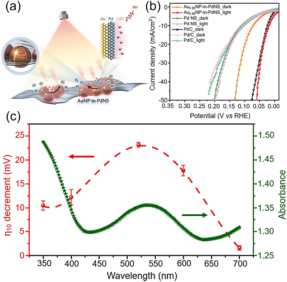 | ||
| Fig. 45 AuNP-in-PdNS for enhanced electrocatalytic activity under LSPR excitation. (a) Proposed mechanism for the plasmon-enhanced ORR and HER. Plasmon-enhanced HER electrocatalysis: (b) Polarization curves collected on the Au0.50NP-in-PdNS, Pd NS, Pt/C and Pd/C electrode at a scan rate of 10 mV s−1 under Xenon light illumination and dark conditions. (c) ORR polarization curves collected for Au0.50NP-in-PdNS electrocatalysts under Xenon light illumination and dark conditions at room temperature. Plasmon-enhanced ORR electrocatalysis: (d) Polarization curves collected on the Au0.50NP-in-PdNS, Pd NS and Pt/C electrode at a scan rate of 10 mV s−1 under Xenon light illumination and dark conditions. Adapted with permission from ref. 742; Copyright 2021 American Chemical Society. | ||
5.3 Plasmon-enhanced biomass energy
There is growing interest in utilizing renewable resources, such as solar energy, as a driving force and biomass-derived compounds as feedstocks for simultaneous hydrogen production. These approaches are recognized as sustainable solutions for energy generation and effective strategies against climate change. Compared to water, organic compounds interact more readily with photo-generated valence band holes, making them more suitable for valorization.743 The process that involves the degradation of organic contaminants, particularly biomass-derived ones, in wastewater under solar irradiation is known as photoreforming.655 However, in the context of photogenerated hydrogen, the quantum efficiency of converting photon energy into hydrogen is typically suboptimal. Metal/semiconductor heterojunctions can induce LSPR, which generates a significant amount of heat in the nanoscale region, creating thermo-photocatalytic conditions without the need for additional heating systems.166,744 Ultimately, the deployment of plasmonic nanocatalysts can substantially enhance photocatalytic activity, especially in the realm of hydrogen (H2) evolution. Fig. 46 presents a schematic diagram of biomass photoreforming on metal/semiconductor catalysts, highlighting the role of metal plasmons as electron sinks that enhance the separation of photo-generated electron–hole pairs. | ||
| Fig. 46 Mechanisms of plasmon-enhanced biomass energy. (a) Metal as a plasmonic enhancer for separating photo-generated e−/h+ pairs. (b) Catalytic role of metal in the dehydrogenation of biomass-derived compounds. | ||
 | ||
| Fig. 47 Plasmon enhanced methanol photoreforming. (a) Schematic model of Pt and Au/TiO2 photocatalysts for methanol reforming. (b) H2, H2CO, CO and CO2 productivity during the photocatalytic steam reforming of methanol. Adapted with permission from ref. 745; Copyright 2013 Elsevier. | ||
 | ||
| Fig. 48 Plasmon enhanced ethanol photoreforming. (a) Production rates of H2, CO2 and C2H4 with pure TiO2 and metal-impregnated TiO2 in a water/ethanol mixture. (b) Estimated H2/CO2 and C2H4/CO2 ratios. Adapted with permission from ref. 746; Copyright 2018 Elsevier. | ||
200 ppm h−1 gcat−1 on the 0.5% Au-loaded WO3/TiO2 photocatalyst (Fig. 49b). This result suggests that plasmonic Au–NPs decorated on WO3/TiO2 heterojunctions facilitate faster charge separation and higher visible light absorption through SPR, leading to improved hydrogen production.
 | ||
| Fig. 49 Plasmon-enhanced glycerol photoreforming. (a) Mechanisms for photocatalytic H2 production from the glycerol–water mixture over WO3/TiO2 with Au–NPs under visible light. (b) Photoactivity evaluation of various photocatalysts: TiO2, WO3/TiO2, 0.5% Au/TiO2, 0.3% Au-WO3/TiO2, 0.5% Au-WO3/TiO2 and 0.7% Au-WO3/TiO2. Adapted with permission from ref. 748; Copyright 2020 Elsevier. | ||
 | ||
| Fig. 50 Plasmon-enhanced glucose photoreforming. (a) Mechanisms for glucose photoreforming over 3DOM TiO2-Au. (b) Glucose conversion rates. (c) Arabinose production with different photocatalysts. Gas products: (d) H2, (e) CH4, and (f) CO with different photocatalysts. Adapted with permission from ref. 752; Copyright 2021 Elsevier. | ||
 | ||
| Fig. 51 Plasmon-enhanced dry reforming of methane. (a) Schematics of enhanced selectivity and stability in photocatalysis via the desorption induced by electronic transitions (DIET) mechanism. (b) Light-to-chemical energy efficiency of photocatalysis as a function of white light intensity. (c) Methane conversion via photocatalytic (blue) and thermocatalytic (red) methods as a function of space velocity. Adapted with permission from ref. 755; Copyright 2020 Springer Nature. | ||
5.4 Plasmon-enhanced thermal energy
Solar thermal energy, obtained through the conversion of solar energy to heat, has emerged as an efficient, clean, economical, and direct method for harnessing renewable energy.756,757 However, conventional solar-thermal collection designs are plagued by significant thermal energy losses and poor thermal stability of the photothermal conversion materials used.758 In recent years, the plasmonic heating effect of noble metal NPs has garnered significant research interest.759–762 The dissipation of LSPPs at visible frequencies can be leveraged to create localized nanoscale heat sources. Meanwhile, noble metals typically exhibit an exceedingly low optical quantum yield, resulting in nearly 100% photothermal conversion efficiency.763 The field of research focusing on the heating effects from plasmonic antennas is known as “thermoplasmonics”.764 To harness this heating effect, thermoplasmonics has been applied across various fields (Fig. 52), including gas sensing, thermal emission control, biomedical applications, and thermal radiation energy management. | ||
| Fig. 52 Applications of thermoplasmonics. | ||
 | ||
| Fig. 53 Efficient solar-thermal energy harvesting via internal plasmonic heating. (a) Schematic of solar-thermal energy harvest driven by interfacial plasmonic heating. (b) Temperature progression profiles for solar water heating systems, comparing conventional and new solar-thermal designs. Adapted with permission from ref. 766; Copyright 2016 American Chemical Society. | ||
 | ||
| Fig. 54 Thermal energy harvesting with plasmonic-based chemical sensors. (a) Schematic of the thermal imaging setup. Calibration graphs from thermal and white light imaging for (b) NO2, (c) H2 and (d) CO analyte gases in an air background. Adapted with permission from ref. 769; Copyright 2014 American Chemical Society. | ||
 | ||
| Fig. 55 Controlling thermal emission with optical absorbers in metasurfaces. (a) Schematic of the sandwich structure. (b) Measured (left) and simulated (right) angle-resolved thermal emission spectra with fixed lattice Λ = 7 μm and a varied grating width d of 3.45 μm. (c) Calculated absorptivity (red) and measured thermal emission (black) spectra vs. wavelength. Adapted with permission from ref. 770; Copyright 2019 American Chemical Society. | ||
 | ||
| Fig. 56 Ultrathin 2D plasmonic PtAg nanosheets for broadband phototheranostics. (a) SH-PEG-FA-modified ultrathin PtAg nanosheets for 4T1 tumor-targeted PTT guided by PAI with 785 and 1064 nm lasers. (b) Photothermal heating trajectories of 4T1 tumors with a 785 nm laser. (c) Photothermal heating trajectories of 4T1 tumors with a 1064 nm laser. (d) Photothermal imaging of 4T1 tumors with a 785 nm laser. (e) Photothermal imaging of 4T1 tumors with a 1064 nm laser. Adapted with permission from ref. 779; Copyright 2021 Wiley. | ||
 | ||
| Fig. 57 Copper plasmonic metamaterial for directional thermal energy management. (a) Sketch of the operating structure. (b) SEM images of the fabricated disk. (c) Absorption spectra with front and back incidence after reduction treatment. (d) Simulated absorption spectra with front and back incidence. Adapted with permission from ref. 782; Copyright 2020 Elsevier. | ||
5.5 Plasmon-enhanced mechanical energy
Since Professor Wang et al. first invented a novel arch-shaped triboelectric nanogenerator (TENG) in 2012,783 various methods have been proposed to improve the output power of a TENG, including surface functionalization, nanoparticle doping, and chemical modification.784–789 However, these approaches primarily alter the surface properties of triboelectric films, often resulting in low efficiency and unstable output. Surface charges are crucial in TENGs, as they not only generate current but also facilitate the conversion of mechanical energy into electrical energy. Therefore, optimizing surface charge density is essential for enhancing TENG efficiency. Recent research has shown that surface plasmon resonance and the excitation of hot electrons can form charge traps when precious metals are introduced into friction materials.657,790 These charge traps can increase the surface charge density of TENGs through a mutual-coupling effect, significantly improving their output power.Chen et al. developed a high-output-power TENG based on charge traps generated by mutual coupling effects within g-C3N4/MXene-Au composites (Fig. 58).791 In this work, g-C3N4 absorbs light energy and generates carriers that act as charge traps. The surface plasmon resonance of Au and its excited hot electrons further contribute to the formation of charge traps. Additionally, the superior electronic transmission capability of MXene facilitates the generation of more charge traps. These charge traps enhance surface charge accumulation in the TENG through mutual coupling effects, resulting in a TENG with the output voltage, current, peak power, and power density of 510 V, 80 μA, 20 mW (4 × 4 cm), and 12.5 μW mm−2 at an impedance of 2 MΩ, respectively. This output power was six times higher than that of a conventional TENG with PDMS.
 | ||
| Fig. 58 Boosting TENG output performance via mutual coupling effects of photon-carriers and plasmon. (a) Mechanism for creating more charge traps. (b) UV-vis spectrum of g-C3N4, MXene, and g-C3N4/MXene-Au composites. (c) Charges of TENG materials under visible light. (d) Output power of the TENG with g-C3N4/MXene-Au composites under visible light. (e) Charge curve of the TENG with g-C3N4/MXene-Au composites under visible light. Adapted with permission from ref. 791; Copyright 2022 Wiley. | ||
The same research group also developed a TENG doped with Ag@SiO2 core–shell particles (Ag@SiO2-NPs), which exhibited high instantaneous power density under visible light illumination (Fig. 59a).657 It was found that Ag@SiO2-NPs alleviated the seepage effect common in conventional nanoparticles and mitigated surface charge leakage typically caused by metal nanoparticles (Fig. 59b). More importantly, the surface plasmon effect enabled the core–shell nanoparticles to further enhance the TENG's output performance (Fig. 59c–j). The peak output power reached 70 mW, the output current was 248 μA, the output power density reached up to 4.375 mW cm−2, and the output voltage exceeded 1 kV when the shell thickness was 6 nm with a doping content of 0.4 wt%, far surpassing the performance of conventional TENGs.
 | ||
| Fig. 59 Surface plasmon effect dominated high-performance TENG. (a) Superiority of Ag@SiO2 NPs in generating the surface plasmon effect. (b) Capacitor model of a TENG, both undoped (upper) and doped with Ag@SiO2 (lower). (c)–(f) Output voltage of Ag, Ag@SiO2-3 nm, Ag@SiO2-6 nm, and Ag@SiO2-12 nm with visible light. (g)–(j) Output power of Ag, Ag@SiO2-3 nm, Ag@SiO2-6 nm, and Ag@SiO2-12 nm with visible light. Adapted with permission from ref. 657; Copyright 2022 AAAS. | ||
Additionally, Gao et al. utilized grating-electrode-enabled surface plasmon excitation in TENGs.790 The generation of hot electron–hole pairs from the decay of surface plasmon resonance effectively enhanced the output performance of TENGs while reducing their output impedance (Fig. 60a–c). Using this method, a peak output power of 3.6 mW was achieved under a loading resistance of 1 MΩ, exhibiting a 4.5-fold enhancement in output power and a 75% reduction in output impedance (Fig. 60d and e).
 | ||
| Fig. 60 Enhancing TENG performance with grating-electrode-enabled surface plasmon excitation. Theoretical model of grating-coupled surface-plasmon-enhanced TENGs: (a) Generation of hot electron–hole pairs. (b) Theoretical models of reverse electric fields from hot electron–hole pairs. (c) Schematic of the TENG with a double-layer structure based on CDs. (d) The output voltage of TENG with aluminum foil at different line densities. (e) The output current of TENG with aluminum foil at different line densities. Adapted with permission from ref. 790; Copyright 2019 Wiley. | ||
5.6 Section summary
This section mainly examines the pivotal role of plasmons in promoting the generation and conversion of green renewable energy. Plasmons can enhance solar energy conversion by increasing the photonic activity of semiconductors, promote the conversion of solar energy into chemical energy through the SPR effect, accelerate the degradation of biomass-derived compounds and the release of hydrogen through plasmonic nanocatalysts, regulate the applications of thermal energy via metallic plasmonics, and increase output power by elevating the surface charge density of TENGs. In summary, plasmon technology demonstrates immense potential in advancing the development of sustainable green energy.Plasmonics has demonstrated potent efficacy in several energy conversion processes; nonetheless, its application in several fields still faces challenges and requires further exploration by researchers. One of the primary challenges is the need to harvest energy from multiple sources. Traditional energy harvesters are often designed to capture a single type of energy, such as solar or mechanical, which limits their functionality when that energy source is unavailable. To address this limitation, integrated energy harvesters that combine multiple energy sources, such as solar cells, biomass energy, thermal energy, and mechanical energy, are essential. These hybrid systems enhance the versatility and efficiency of energy harvesting devices, allowing them to operate effectively across a broader range of scenarios. However, designing and optimizing these integrated systems to work harmoniously presents significant technical challenges.
Another challenge in conversion applications is the efficient use of the full solar spectrum. Plasmonic devices typically operate within a narrow spectral range, which limits their ability to harness energy across the entire spectrum. This restriction poses a significant obstacle for widespread energy harvesting applications. Recent advances in multifunctional plasmon materials, which can modulate electron density and temperature, offer a potential solution. By tailoring these materials to respond to different wavelength bands, it is possible to create devices that can capture energy from the entire solar spectrum. However, achieving this level of control and efficiency remains a complex challenge in material design and engineering.
As energy harvesting devices become more portable and miniaturized, maintaining efficiency and stability becomes increasingly difficult. Smaller plasmonic energy harvesters often suffer from reduced energy density, which can limit their practical applications. To overcome this challenge, researchers are exploring the use of flexible, lightweight, and highly conductive materials, along with nanotechnology, to design smaller, more efficient components.792,793 These advancements could lead to the development of portable energy harvesters suitable for wearable technology, drones, and mobile power applications. However, balancing miniaturization with performance and reliability remains a key challenge.
6. Integrated plasmonic circuits
The rapid downsizing of electronic components to the submicron scale has brought about remarkable increases in computing power, coupled with significant cost reductions. As the microelectronics industry continues its journey towards smaller devices, it becomes increasingly plausible that both physical and economic constraints associated with top-down silicon technology will soon impose limitations on further progress. To overcome these limitations and meet the anticipated demands of future society, revolutionary breakthroughs, rather than incremental advances, are imperative. A promising avenue involves a paradigm shift from electronic signals to light. However, utilizing electromagnetic waves as information carriers in optical signal-processing devices and PICs faces a formidable challenge—the limited integration and miniaturization available.794 This challenge is intricately linked to the diffraction limit of light in dielectric media, preventing the confinement of electromagnetic waves into nanoscale regions significantly smaller than the wavelength of light. Addressing this issue requires innovative approaches, and one captivating method involves leveraging the unique properties of plasmonic nanomaterials. Consequently, proposals for photonic components and electronic circuits based on localized plasmonic resonance have surfaced, demonstrating potential in tackling the scalability and performance challenges associated with future plasmonic integrated circuits (Fig. 61).795 This approach holds the promise of achieving all-optical processing of optical signals, thereby enhancing the speed, bandwidth, and overall capacity of information technology. Simultaneously, it presents an opportunity to reduce costs and power consumption, aligning with the evolving needs of future communication, computing, sensing, and other fields. This section provides an overview of recent strides in integrated electronic circuits grounded in plasmonic properties, including plasmonic emitters, plasmonic modulators/switchers, plasmonic logic gates, and plasmonic detectors. | ||
| Fig. 61 Overview of plasmonic integrated circuit components featuring high functionality on small wafer footprints. Adapted with permission from ref. 795; Copyright 2012 Springer Nature. | ||
6.1 Plasmonic emitters
Plasmonic emitters or lasers represent a cutting-edge approach to addressing the challenges of creating highly compact plasmonic circuits. Unlike traditional lasers that amplify light, plasmonic lasers operate by amplifying surface plasmons, which are collective oscillations of electrons at the interface between a metal and a dielectric. This fundamental difference results in unique operational characteristics, particularly due to the strongly confined electromagnetic fields in a plasmonic laser cavity. One of the key features of plasmonic lasers is their ability to significantly enhance the spontaneous emission rate via the Purcell effect.796 The Purcell effect, named after the physicist Edward Purcell, describes how the spontaneous emission rate of an emitter can be modified by its surrounding electromagnetic environment. In the context of plasmonic lasers, the extremely confined electromagnetic fields in the nanocavity result in a dramatically reduced effective mode volume. According to the Purcell formula Fp ∝ Q/V, a smaller mode volume (V) and a sufficiently high quality factor (Q) lead to a larger Purcell factor (Fp), meaning the spontaneous emission rate is enhanced compared to an emitter in free space. This effect is particularly pronounced in low-dimensional plasmonic nanostructures, where the enhancement scales anomalously with frequency. The confined fields and the Purcell enhancement enable the plasmonic laser to achieve exceptionally fast response times, even at wavelengths far from the surface plasmon resonance.The enhancement of the spontaneous emission rate is quantified by the β-factor, which represents the fraction of spontaneous emission coupled into the laser mode compared to all other modes. A high β-factor is critical because it reduces the threshold for stimulated emission, potentially allowing plasmonic lasers to operate with lower thresholds despite the inherent high losses in metal–dielectric nanostructures. However, it is important to note that while the promise of low-threshold plasmonic lasers is significant, current implementations still face considerable challenges. The high intrinsic ohmic losses in metals contribute to relatively high lasing thresholds, which is a major barrier that researchers continue to address. Despite this, the potential for plasmonic lasers to revolutionize ultra-compact photonic circuits keeps them at the forefront of nanophotonics research.
 | ||
| Fig. 62 Plasmonic emitters. (a) Plasmonic CdS emitter. (I) Schematic representation of the plasmonic CdS emitter. (II) Working mechanism. (III) The emission spectra and polarization-dependent behavior of the emitter. Adapted with permission from ref. 797; Copyright 2013 American Chemical Society. (b) Plasmonic perovskite emitter for free-space excitation. Adapted with permission from ref. 798; Copyright 2018 American Chemical Society. (c) Plasmonic perovskite emitter for waveguides in confined modes. (I) Schematic representation of the emitter. (II) Micro-photoluminescence image of the emitter pumped above the lasing threshold. (III) Spectra from the end of the waveguide. Adapted with permission from ref. 799; Copyright 2022 the Royal Society of Chemistry. (d) Plasmonic tunable emitter by stretching and releasing the elastomeric substrate. Adapted with permission from ref. 800–802; Copyright 2022 American Chemical Society. (e) Plasmonic tunable emitter by using liquid gain materials (IR-140 dye molecules). Optically pumped arrays of gold nanoparticles surrounded by IR-140 dye molecules are tuned as a function of the dielectric environment. Adapted with permission from ref. 803–806; Copyright 2015 Springer Nature. | ||
6.2 Plasmonic modulators and switches
Optical modulators are essential components in modern photonic systems, enabling the control of light signals in various applications, from telecommunications to sensing and imaging. The primary function of an optical modulator is to manipulate the properties of light—such as amplitude, phase, or polarization—by an external signal, typically electrical or optical. This modulation allows for the encoding, switching, and routing of data within photonic circuits, making optical modulators key enablers for high-speed and high-bandwidth communication systems. While traditional optical modulators have proven effective for a wide range of applications, the demand for more compact, faster, and energy-efficient devices has led to the exploration of alternative technologies. Among these, plasmonic modulators have gained significant attention due to their ability to confine light to subwavelength dimensions, thereby enhancing light–matter interactions far beyond the capabilities of conventional modulators.Plasmonic modulators leverage the unique properties of surface plasmons—coherent oscillations of electrons at the interface between a metal and a dielectric. These oscillations can be strongly confined to nanoscale regions, leading to several key advantages: (1) ultra-compact size: plasmonic modulators can be much smaller than traditional optical modulators because they operate at the nanoscale, confining light to volumes much smaller than the wavelength of light. This miniaturization is critical for high-density integration in photonic circuits, allowing for more compact and scalable designs; (2) high-speed operation: the enhanced light–matter interaction in plasmonic structures enables faster modulation speeds, often in the terahertz range. This makes plasmonic modulators ideal for high-speed data transmission and processing, far surpassing the capabilities of conventional modulators; and (3) enhanced modulation depth: the strong field enhancement associated with surface plasmons allows for greater modulation depth, meaning that the degree of change in the optical signal is more pronounced. This can lead to higher signal contrast and improved performance in optical communication systems.
 | ||
| Fig. 63 Plasmonic modulators. (a) Plasmonic modulator operating at 40 Gbit/s based on electro-optic modulation in a nonlinear polymer. (I) Schematic representation of the modulator. (II) SEM image of the device. (III) Modulation experiment results. Adapted with permission from ref. 809; Copyright 2014 Springer Nature. (b) Plasmonic modulator operating at 408 Gbit/s based on thermo-optic modulation. (I) Schematic representation of the device. (II) High-speed transmission experiment. (III) Eye diagrams and signal-to-noise ratios (SNRs) for 220Gbps, 320Gbps, and 408Gbps transmission. Adapted with permission from ref. 810; Copyright 2023 Springer Nature. | ||
The PPM consists of two metal tapers that facilitate the conversion between photonic and plasmonic modes, and a phase modulator section located between them. The metal taper, which narrows at an angle of 15°, acts as an interface between the silicon photonics and plasmonics, enabling efficient excitation of the plasmonic resonance by light guided through a silicon nanowire. The device is exceptionally compact, with a length of just 29 μm. It also has a flat modulation frequency response up to at least 65 GHz and maintains thermal stability up to 85 °C.
6.3 Plasmonic logic gates
Optical logic circuits represent a significant advancement in computing technology, leveraging the properties of light for processing and transmitting information. Unlike traditional electronic logic circuits that rely on electrical signals, optical logic circuits use photons, the fundamental particles of light, to perform logical operations such as AND, OR, NOT, and XOR. This transition from electronic to optical systems is driven by several factors, including the need for higher data transmission speeds, lower power consumption, and the miniaturization of components. Despite these advantages, optical logic circuits face challenges, including the need for continuous power to maintain operations (volatility), large device footprints due to weak interaction effects, and difficulties in achieving compact designs. Plasmonic logic circuits leverage the strong confinement of electromagnetic fields in plasmonic structures, which enhances light–matter interactions. This strong interaction allows for more efficient modulation and switching, thereby reducing the power required for operation. Additionally, plasmonic circuits excel at confining light to dimensions much smaller than the wavelength of light. The confinement occurs at the nanoscale, which allows plasmonic devices to be significantly smaller than their purely optical counterparts. | ||
| Fig. 64 Integrated electro-plasmonic logic circuits. (a) Schematic of the plasmonic slot waveguide for integrated logic circuits. The amorphous phase and crystalline phase of PCM (Ge2Sb2Te5) are used for switching of waveguide modes. (b) Schematic diagram of waveguide mode switching and the corresponding optical electric field distribution. (c) Non-volatile fundamental EO logic operations of AND, OR, NAND, and NOR logic. (d) Sequential logic circuits. Upper panel: JK latch circuit. Lower panel: T latch circuit. Adapted with permission from ref. 811; Copyright 2021 Springer Nature. | ||
In addition to PCMs, electro-plasmonic logic circuits also explore other materials that offer unique advantages, such as graphene, transition metal dichalcogenides (TMDs), and transparent conductive oxides (TCOs). In electro-plasmonic circuits, graphene can be used to achieve dynamic modulation of plasmonic signals. By applying a voltage, the carrier density in graphene can be modulated, leading to significant changes in its plasmonic resonance. This property makes graphene a promising candidate for developing ultrafast, tunable plasmonic devices with broad operational bandwidth. Besides, materials such as molybdenum disulfide (MoS2) and tungsten diselenide (WSe2) exhibit strong light–matter interactions, making them suitable for use in plasmonic circuits. TCOs, such as indium tin oxide (ITO), can be used to modulate plasmonic waves by applying an electric field, which alters the carrier concentration in the material. This change can modulate the refractive index, enabling the implementation of plasmonic logic functions with minimal optical losses.
All-optical plasmonic logic gates represent a significant advancement in the field of photonic computing, particularly in the context of free-space excitation. Unlike electro-plasmonic logic circuits, which rely on electrical signals to modulate plasmonic waves, all-optical plasmonic logic gates exclusively utilize light for both input and output operations. Plasmons in the device interact with each other to produce interference patterns, which are the basis for logical operations. The key advantages of this approach are the elimination of electrical interconnects, which can introduce delays and consume more power, and the potential for extremely high-speed operation due to the inherently fast nature of light–matter interactions.
 | ||
| Fig. 65 All-optical plasmonic logic gates in free-space excitation. (a) Plasmonic metal logic gate. (I) Schematic illustration of the logic gate NOR. (II) Optical image of the plasmonic logic gate using the designed Ag NW structure. (III) The scattering images showing the various logic operations. Adapted with permission from ref. 812; Copyright 2011 Springer Nature. (b) Plasmonic organic/metal logic gate. (I) Schematic illustration of the organic nanowire as the logic gate. (II) Spatial relationship between transition dipole moment and preferred growth direction of organic nanowires. (III) Bright-field and photoluminescence microscopy images of the hybrid nanostructure excited at different polarization angles. (VI) Photoluminescence microscopy images of the device for logic processing. (V) Graphical symbol, scattering spectra, and truth table of the logic processing. Adapted with permission from ref. 813; Copyright 2012 John Wiley and Sons. | ||
6.4 Plasmonic detectors
In plasmonic PICs, following the generation, routing, and modulation of surface plasmons, the data must be converted from the optical domain into the electrical domain, which is typically achieved via a photodetector. Integrated plasmonic detectors offer several advantages over conventional photodetectors, particularly in photonic-plasmonic hybrid circuits. These advantages include higher integration densities, low device capacitance for fast transit times leading to higher bandwidth operations, and reduced operational energy due to enhanced light–matter interactions. As detectors are scaled down in size, the response time improves, but this miniaturization often comes at the cost of reduced sensitivity and responsivity, primarily due to diminished absorption in the detector's semiconductor material. This presents a challenge, as maintaining high sensitivity and responsivity is critical for effective photodetection.The challenge of reduced absorption in miniaturized detectors can be addressed through the use of emerging active plasmonics. Plasmonic detectors can enhance material absorption through mechanisms similar to the Purcell effect observed in plasmon nanolasers, where spontaneous emission is enhanced. Achieving strong photo-absorption involves increasing the local density of states within the absorbing semiconductor region without introducing unwanted quenching channels.
 | ||
| Fig. 66 Plasmonic detectors. (a) Plasmonic zero-bias metal-graphene detector. (I) Schematic illustration of the zero-bias detector. (II) Simulated near-field distribution and predicted vectorial photocurrent in a unit cell at different polarization angles of incident light (Pol). (III) Polar plot of measured photocurrents. (IV) Schematic of the experimental setup. (V) SEM images and measured photovoltage of three devices with different degrees of asymmetry. Adapted with permission from ref. 634; Copyright 2020 Springer Nature. (b) Plasmonic metal–semiconductor–metal detector. (I) Schematic illustration of the metal–semiconductor–metal detector. (II) Spectral responses of the detectors. Adapted with permission from ref. 814; Copyright 2009 Springer Nature. (c) Plasmonic metal–metal detector. (I) Schematic illustration of the metal–metal detector. (II) A simplified energy level diagram of the tunnel junction with bias showing the working mechanism. (III) Response current density of the detector in the frequency domain. Adapted with permission from ref. 815; Copyright 2017 Springer Nature. | ||
Overall, the development of plasmonic detectors represents a significant advancement in PICs, offering the potential for high-speed, low-power, and highly integrated optical-electrical conversion. These detectors are crucial components in the ongoing evolution of plasmonic circuits, enabling new functionalities and improving the performance of photonic systems.
6.5 Section summary
This section reviews recent advances in integrated electronic circuits leveraging plasmonic properties. It covers plasmonic emitters, modulators/switchers, logic gates, and detectors, and highlights their role in pushing the boundaries of next-generation electronics. Despite these strides, significant challenges remain in PIC applications.One of the foremost challenges in plasmonic PICs is managing energy attenuation, a persistent issue in both electronic and plasmonic circuits. In electronic circuits, transistors modulate gate voltages and currents to process signals, while in plasmonic circuits, signal processing is reliant on the propagation of light intensity and polarization. This shift in paradigm requires the integration of repeaters and switches, with quantum dots serving as signal amplification materials. By directing excitation light onto waveguides, these repeaters can amplify signals while maintaining their original characteristics. However, the energy consumption within these integrated circuits primarily arises from scattering at junctions, thermal losses, and amplification materials for the light source. While heating losses are inevitable, they are relatively minor compared to scattering losses at junctions. Implementing total internal reflection dielectric covers at these junctions can significantly reduce energy waste. Despite these challenges, the overall energy consumption of plasmonic chips is anticipated to be considerably lower than that of electronic chips, as all operations are based on the propagation and interference of plasmons rather than electrical currents.
Another significant challenge is the fabrication of the various components on a single platform. PICs involve multiple elements, including plasmonic emitters, modulators, logic gates, switchers, and detectors, each with its own set of fabrication requirements. Achieving high levels of integration while ensuring compatibility between these diverse elements is a complex task. The fabrication process must address issues such as material compatibility, precision alignment, and minimizing losses at interfaces between different components. Additionally, the scale at which these components must be manufactured adds another layer of complexity, as even minor imperfections can lead to significant performance degradation. Overcoming these challenges is crucial for the development of fully integrated plasmonic PICs that can meet the demands of modern optical communication systems.
Heat management and loss reduction are also critical challenges in plasmonic PICs. As plasmonic circuits operate at the nanoscale, they are prone to significant heat generation, especially at junctions where scattering and material imperfections can lead to increased losses. Managing this heat is vital for maintaining the stability and performance of the circuits. Advanced materials and design techniques, such as incorporating thermal conductive layers or using materials with lower scattering losses, are being explored to mitigate these issues. However, striking a balance between reducing heat generation and maintaining efficient signal propagation remains a delicate challenge.
7. Conclusions and future perspectives
7.1 Conclusions
In summary, we present a detailed and comprehensive review of integrative plasmonics—from underlying mechanisms to device applications. It begins by exploring various optical phenomena in plasmonics, such as plasmon–phonon coupling, nonlinear optical effects, EIT, plasmonic chirality, nanocavity resonance, and waveguide resonance. The discussion then extends to advanced strategies for enhancing plasmonic responses beyond traditional single-effect phenomena. These include designing hybrid nanostructures to confine light at subwavelength scales and boost near-field interactions. Utilizing 2D materials such as graphene for dynamic tuning promotes stronger field enhancements and nonlinear processes. Then, we emphasize the synergy between plasmonic effects and other domains including acoustics, electronics, and thermal technologies. For example, plasmon-induced local heating can trigger thermoacoustic effects that generate ultrasound for high-contrast imaging or even for therapeutic interventions like tumor ablation. Collectively, these fusion strategies are paving the way for multifunctional platforms capable of simultaneous imaging, sensing, and treatment, thereby broadening applications in molecular diagnostics, energy conversion, and PICs.Based on these discussions, several key advantages of plasmonic optical multi-effects and electric-acoustic-thermal fusion emerge.
(1) Enhanced device performance: multi-effects, such as those derived from plasmon–phonon coupling, significantly improve the overlapping of molecular fingerprint spectra in infrared spectroscopy.47 Besides, they lead to increased sensitivity and lower detection limits in molecular diagnostics, higher conversion efficiency in energy harvesting, reduced energy consumption and extended transmission distances in photonic circuits, and more.
(2) Enabling new functionalities: integrative plasmonics allows for the realization of new functionalities that are challenging to achieve with single-field technologies. For instance, the fusion of plasmonic and BPVE facilitates zero-bias photodetection,634 a capability that traditional approaches struggle to deliver.
(3) Expanded application range: by combining plasmonic effects with acoustic, photoelectric, and thermal technologies, integrative plasmonics enables the simultaneous execution of multiple functions, such as imaging, diagnosis, and treatment, within a single platform.209 This multifunctionality is particularly valuable in medical diagnostics and therapy, where integrated approaches can lead to more comprehensive and effective solutions.
7.2 Challenges
While the works highlighted in this review offer promising solutions for integrative plasmonics, the field remains in its early stages due to the complexity of multiple mechanisms and interdisciplinary approaches. Currently, integrative plasmonics still faces challenges. Below are some personal insights into these challenges. It is important to note that listing these challenges is intended to foster timely discussion and progress in the field, rather than to diminish the efforts of many colleagues or the significant advances already made.(1) Challenges in integrating optical multi-effects on the same platform. Designing multi-functional nanostructures in plasmonics is challenging, as it requires integrating multiple optical effects while optimizing different plasmonic modes with varying spatial, spectral, and material requirements. Effect synergy and optimization pose additional difficulties, as different plasmonic effects, such as SERS, SEF, and LSPR, often have conflicting design requirements and resonant conditions, making their integration complex. Balancing the spatial distribution of localized electromagnetic fields is another critical challenge, as different effects require specific field configurations, demanding precise control over nanostructure geometry, size, and material composition to ensure optimal performance.
(2) Challenges in fusing acousto-optical-electric-thermal effects via plasmons. Integrating optical, electric, acoustic, and thermal mechanisms in plasmonics is challenging due to their distinct operational principles and requirements. A major difficulty lies in designing plasmonic systems that effectively combine these diverse effects while maintaining high performance. The lack of a comprehensive theoretical framework further complicates integration, as existing models are specialized and do not fully describe cross-domain interactions. Additionally, finding materials that perform well across all domains is difficult, as most are optimized for only one or two effects. Hybrid or composite materials offer a potential solution but require careful design to achieve balanced multifunctionality.
(3) Challenges in molecular diagnostics applications based on integrative plasmonics. A primary challenge in plasmonic biosensing is achieving high sensitivity across various techniques, such as SERS and SEIRAS, by optimizing hotspot enhancement. This requires developing materials and structures that amplify weak signals from low-concentration analytes while maintaining high sensitivity across different spectral regions. Ensuring selectivity in complex biological environments is another challenge, as background interference can compromise molecular specificity. Reproducibility is also critical, with variability in substrate manufacturing and environmental conditions affecting consistent performance. Stability of plasmonic substrates under fluctuating experimental conditions is essential for reliable long-term applications, especially in clinical diagnostics. Finally, cost-effectiveness remains a significant challenge, particularly in point-of-care testing, where affordable, scalable manufacturing is needed for widespread implementation.
(4) Challenges in energy conversion applications. Firstly, multifunctional and highly efficient integrated energy harvesters are capable of capturing energy from a variety of sources, but their design and optimization require further in-depth exploration to enable their application in a broader range of operational scenarios. Additionally, in the material design and engineering of plasmon-enhanced energy conversion, achieving effective utilization of the entire solar spectrum and exerting control over broadband energy capture remain a complex endeavor. Furthermore, achieving a balance between miniaturization and performance, as well as reliability, in plasmonic energy harvesters remains a pivotal challenge.
(5) Challenges in plasmonic PICs. Plasmonic PICs face challenges in managing energy attenuation, primarily due to scattering losses at junctions and thermal dissipation. Implementing repeaters with quantum dots and total internal reflection dielectric covers can help mitigate these losses. Fabrication complexity is another issue, as integrating diverse components like emitters, modulators, and detectors requires precise alignment and material compatibility. Heat management is also critical, as nanoscale plasmonic circuits generate significant thermal losses, necessitating advanced materials and design strategies to balance efficiency and stability.
7.3 Future perspectives
Looking forward to the future development of integrative plasmonics, efforts can be invested along the current development path to solve the above challenges. Additionally, based on the advances made in integrative plasmonics, some personal insights are proposed to propel the discipline toward sustained, high-quality progress in mechanism advancements, material innovations, technological breakthroughs, and application expansion, as illustrated in Fig. 67.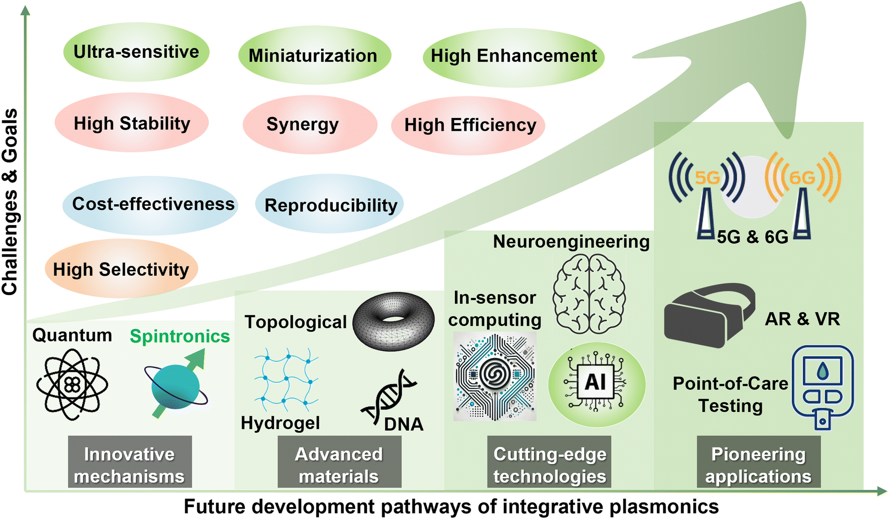 | ||
| Fig. 67 Challenges, goals, and future development pathways of integrative plasmonics. | ||
(2) Spintronics and plasmonics: spintronics, which exploits the spin of electrons in addition to their charge, offers new possibilities for manipulating light–matter interactions in plasmonic systems. The integration of spintronic principles with plasmonics, often referred to as spin-plasmonics, has the potential to create devices that utilize the spin degree of freedom to control plasmonic excitations. This can lead to novel applications in information processing, where the combination of spintronics and plasmonics could enable the development of spin-based plasmonic transistors, spin filters, and logic gates. Recent research has shown that materials such as ferromagnetic metals and topological insulators can be used to control plasmonic modes via spin–orbit coupling, making spin-plasmonics a promising area for future exploration.820
(3) Topological plasmonics: topological photonics, which draws on concepts from topological insulators, explores the robust propagation of light along the edges of photonic structures without backscattering.821 When combined with plasmonics, topological plasmonics can enable the creation of plasmonic modes that are immune to defects and disorders, thus offering new routes for robust and energy-efficient photonic devices. Early research in this area has demonstrated the existence of topologically protected plasmonic edge states in certain photonic crystals and metamaterials.822 These edge states could be utilized in applications such as robust plasmonic waveguides, sensors, and on-chip communication devices, where immunity to scattering and losses is crucial.
(2) Biomolecule-based plasmonic nanocomposites: plasmonic materials combined with biological molecules, such as DNA, represent a cutting-edge area of research with tremendous potential, particularly in biosensing, nanomedicine, and molecular electronics.825 These hybrid materials leverage the unique properties of both plasmonic nanoparticles and biological macromolecules, offering new functionalities that are not possible with traditional materials. Below are some of the most promising avenues for this kind of material: (I) DNA-directed assembly of plasmonic nanostructures: DNA's ability to specifically bind to complementary sequences makes it an excellent tool for directing the assembly of plasmonic nanoparticles into well-defined structures.826 This DNA-mediated assembly allows for the precise control of nanoparticle spacing and orientation, which is crucial for tuning the plasmonic properties of the resulting nanostructures. For example, DNA can be used to create dimers, trimers, or even larger assemblies of gold or silver nanoparticles, leading to plasmonic “hot spots” where electromagnetic fields are highly concentrated.827 These hot spots are particularly valuable in SERS and other plasmonic sensing applications, where the sensitivity of detection is greatly enhanced. (II) DNA origami and plasmonic nanostructures: DNA origami involves folding a long single-stranded DNA molecule into complex shapes with the help of short “staple” strands.828 This method allows for the creation of nanoscale structures with precise geometries. When combined with plasmonic nanoparticles, DNA origami can be used to position these nanoparticles with nanometer precision, creating custom-designed plasmonic structures with tailored optical properties. (III) Plasmonic nanoswitches based on DNA conformation changes: DNA molecules can undergo significant conformational changes in response to various stimuli, such as changes in ionic strength, temperature, or the binding of specific ligands.829 These conformational changes can be exploited to create plasmonic nanoswitches, where the optical properties of plasmonic nanoparticles are modulated by the state of the attached DNA molecules.
(3) Plasmon–hydrogel hybrids: plasmonic materials combined with hydrogels represent an exciting and rapidly developing area of research.830 The combination of these two materials results in a versatile platform with a wide range of potential applications, particularly in biosensing, drug delivery, and smart materials. Below are some of the most promising avenues for this kind of material: (I) stimuli-responsive plasmonic hydrogels: hydrogels can respond to various external stimuli, such as pH, temperature, light, and the presence of specific chemicals or biomolecules.831 When plasmonic nanoparticles (e.g., gold or silver nanoparticles) are embedded within a hydrogel matrix, the hybrid material can exhibit significant changes in its optical properties in response to these stimuli. This change is primarily due to the alteration of the interparticle distance within the hydrogel, which affects the plasmonic coupling between the nanoparticles. (II) Plasmonic hydrogels for controlled drug delivery: one of the most promising applications of plasmon–hydrogel hybrids is in controlled drug delivery.832 The hydrogel matrix can encapsulate drugs, while the plasmonic nanoparticles enable remote control over the release of these drugs through light-induced heating. When exposed to specific wavelengths of light, the plasmonic nanoparticles generate localized heat (via the photothermal effect), which can induce the hydrogel to undergo a phase transition (e.g., from a swollen to a collapsed state), releasing the encapsulated drugs in a controlled manner. (III) Optomechanical actuators: plasmon–hydrogel composites can also be used to create optomechanical actuators.833 These are devices that convert optical energy into mechanical motion. When plasmonic nanoparticles embedded in a hydrogel absorb light, the localized heating can cause the hydrogel to swell or shrink, resulting in mechanical movement. This optomechanical response can be finely tuned by adjusting the composition of the hydrogel and the size, shape, and concentration of the plasmonic nanoparticles.
(2) Edge computing and in-sensor computing: edge computing involves processing data closer to the data source, minimizing latency and reducing the need for data to be sent to centralized servers. Plasmonic sensors can be integrated into edge computing systems to provide real-time, on-site data processing with high sensitivity and specificity. The strong LSPR of plasmonic nanostructures enables the detection of minute changes in the local environment, making them ideal for applications where rapid and precise measurements are critical.840 In-sensor computing takes the concept of edge computing further by embedding computational capabilities directly within the sensor itself. This approach allows for the immediate processing of data at the point of capture, reducing the need for data transmission and enabling even faster decision-making.841 Key advantages include reduced latency, high energy efficiency, reduced data bottlenecks, and autonomous decision-making.
(3) Integrating plasmonics with optogenetics and neuroengineering: optogenetics traditionally uses light to control neurons and other cells that have been genetically modified to express light-sensitive ion channels. By combining plasmonic nanostructures with optogenetic tools, researchers can enhance the spatial and temporal resolution of light delivery, as well as introduce new functionalities that were previously unattainable. For instance, in the absence of NIR-activated opsins, upconversion nanoparticles can be used as light-emitting transducers for nanoparticle-mediated optogenetics.842 In neuroengineering, plasmonics can improve neural interface performance.843 By using plasmonic nanoparticles to enhance the delivery and localization of light, more precise control of neuronal activity can be achieved. This enhanced precision is crucial for mapping neural circuits and understanding brain function. Moreover, plasmonic nanoparticles can generate localized heat through thermoplasmonic effects, which can be used to modulate neural activity in a controlled manner. For example, AuNRs can be used to activate temperature-sensitive ion channels in neurons, allowing for precise neuromodulation using NIR light.844 This approach reduces the need for invasive procedures, as NIR light can penetrate deeper into tissues compared to visible light.
(2) Augmented reality (AR) and virtual reality (VR): the demand for more immersive AR and VR experiences is driving the need for advanced optical components that can deliver high-resolution, real-time visual processing.847–849 Plasmonics can significantly enhance AR/VR technologies by enabling the development of miniaturized, high-performance optical devices such as lenses, waveguides, and holographic displays.850 Plasmonic meta-surfaces, for example, can manipulate light with sub-wavelength precision, enabling the creation of ultra-thin, flat optical elements that can be seamlessly integrated into AR glasses or VR headsets.851 These plasmonic components can improve image quality, reduce latency, and enhance the overall user experience by providing faster and more accurate visual processing.
(3) Point-of-care testing (POCT): POCT represents a paradigm shift in medical diagnostics by enabling rapid, on-site testing at the patient's location, such as in a doctor's office, clinic, or even at home.852,853 The incorporation of plasmonic technologies into POCT platforms offers several advantages. Plasmonic-based POCT devices can provide real-time results with high accuracy and sensitivity, which are crucial for the timely diagnosis and management of diseases. These devices can be miniaturized and designed for ease of use, allowing non-specialists to perform complex diagnostic tests quickly and accurately. For instance, plasmonic-enhanced lateral flow assays, which are widely used in POCT, can offer improved sensitivity for detecting biomarkers related to infectious diseases, cancer, and cardiovascular conditions.88
Data availability
No primary research results, software or code have been included and no new data were generated or analysed as part of this review.Conflicts of interest
There are no conflicts to declare.Acknowledgements
This work was supported by the Ministry of Education (MOE) of the Singapore under the research grant R-263-000-F18-112/A-0009520-01-00; Manufacturing, Trade, and Connectivity (MTC) Industry Alignment Fund – Pre-Positioning (IAF-PP) program (Grant No. M23M5a0069), A-8002184-00-00; Manufacturing, Trade, and Connectivity (MTC) White Space Fund (Grant No. M24W1NS005), A-8002323-00-00; and National Research Foundation (NRF) under the Mid-sized grant project (Grant No. NRF-MSG-2023-0002).References
- R. W. Wood, London, Edinburgh Dublin Philos. Mag. J. Sci., 2009, 4, 396–402 CrossRef.
- J. C. Maxwell-Garnett, Philos. Trans. R. Soc., A, 1904, 203, 385–420 Search PubMed.
- M. Fleischmann, P. J. Hendra and A. J. McQuillan, Chem. Phys. Lett., 1974, 26, 163–166 CrossRef CAS.
- A. Hartstein, J. R. Kirtley and J. C. Tsang, Phys. Rev. Lett., 1980, 45, 201–204 CrossRef CAS.
- M. Moradi, M. Jäger, G. R. Newkome and U. S. Schubert, J. Mater. Chem. C, 2023, 11, 1610–1647 RSC.
- J. Xie, Z. Ren, H. Zhou, J. Zhou, W. Liu and C. Lee, Adv. Opt. Mater., 2024, 2401582 CrossRef CAS.
- J. S. Lin, X. D. Tian, G. Li, F. L. Zhang, Y. Wang and J. F. Li, Chem. Soc. Rev., 2022, 51, 9445–9468 RSC.
- Y. Kitajima, H. Sakamoto and K. Ueno, Nanoscale, 2021, 13, 5187–5201 RSC.
- A. V. Kabashin, V. G. Kravets and A. N. Grigorenko, Chem. Soc. Rev., 2023, 52, 6554–6585 RSC.
- D. You, R. Wang, J. Xie, L. Liu, K. Li, X. Han, T. Guo and C. Xu, J. Mater. Chem. A, 2022, 10, 14078–14089 RSC.
- P. Pienpinijtham, Y. Kitahama and Y. Ozaki, Nanoscale, 2022, 14, 5265–5288 RSC.
- S.-L. Peng, G.-Y. Chen and S.-W. Hsu, J. Mater. Chem. C, 2022, 10, 16573–16582 RSC.
- R. F. Oulton, V. J. Sorger, D. A. Genov, D. F. P. Pile and X. Zhang, Nat. Photonics, 2008, 2, 496–500 CrossRef CAS.
- J. Wei, C. Xu, B. Dong, C.-W. Qiu and C. Lee, Nat. Photonics, 2021, 15, 614–621 CrossRef CAS.
- T. Yan, M. Su, Z. Wang and J. Zhang, Small, 2023, 19, e2300539 CrossRef PubMed.
- Y.-K. Liao, Y.-S. Lai, F. Pan and Y.-H. Su, J. Mater. Chem. A, 2023, 11, 11187–11201 RSC.
- W. Jiang, D. Sun, C. Cai and H. Zhang, Analyst, 2023, 148, 3791–3797 RSC.
- N. Hildebrandt, M. Lim, N. Kim, D. Y. Choi and J. M. Nam, Chem. Commun., 2023, 59, 2352–2380 RSC.
- J. Dey, A. Virdi and M. Chandra, Nanoscale, 2023, 15, 17879–17888 RSC.
- X. Zhuo, S. Li, N. Li, X. Cheng, Y. Lai and J. Wang, Nanoscale, 2022, 14, 8362–8373 RSC.
- B. Zhang, T. Kong, C. Zhang, X. Mi, H. Chen, X. Guo, X. Zhou, M. Ji, Z. Fu, Z. Zhang and H. Zheng, Nanoscale, 2022, 14, 16314–16320 RSC.
- F. O. Yevtushenko, S. V. Dukhopelnykov, Y. G. Rapoport, T. L. Zinenko and A. I. Nosich, RSC Adv., 2022, 12, 4589–4594 RSC.
- M. Wang, Y. Yu, S. Prucnal, Y. Berencen, M. S. Shaikh, L. Rebohle, M. B. Khan, V. Zviagin, R. Hubner, A. Pashkin, A. Erbe, Y. M. Georgiev, M. Grundmann, M. Helm, R. Kirchner and S. Zhou, Nanoscale, 2022, 14, 2826–2836 RSC.
- M. Wagner, A. Seifert and L. M. Liz-Marzan, Nanoscale Horiz., 2022, 7, 1259–1278 RSC.
- F. Pan, C. C. Wu, Y. L. Chen, P. Y. Kung and Y. H. Su, Nanoscale, 2022, 14, 13532–13541 RSC.
- A. Lishchuk, E. Csanyi, B. Darroch, C. Wilson, A. Nabok and G. J. Leggett, Chem. Sci., 2022, 13, 2405–2417 RSC.
- C. W. Moon, M. J. Choi, J. K. Hyun and H. W. Jang, Nanoscale Adv., 2021, 3, 5981–6006 RSC.
- F. M. Balci, S. Sarisozen, N. Polat, C. M. Guvenc, U. Karadeniz, A. Tertemiz and S. Balci, Nanoscale Adv., 2021, 3, 1674–1681 RSC.
- C. Clavero, Nat. Photonics, 2014, 8, 95–103 CrossRef CAS.
- A. D. Semenov, G. N. Goltsman and R. Sobolewski, Supercond. Sci. Technol., 2002, 15, R1–R16 CrossRef CAS.
- T. P. White and K. R. Catchpole, Appl. Phys. Lett., 2012, 101, 073905 CrossRef.
- M. Kumar, J. Dey, M. S. Verma and M. Chandra, Nanoscale, 2020, 12, 11612–11618 RSC.
- J. A. Jackman, A. Rahim Ferhan and N. J. Cho, Chem. Soc. Rev., 2017, 46, 3615–3660 RSC.
- L. Wang and G. Arrabito, Analyst, 2015, 140, 5821–5848 RSC.
- A. Campion and P. Kambhampati, Chem. Soc. Rev., 1998, 27, 241–250 RSC.
- J. F. Li, C. Y. Li and R. F. Aroca, Chem. Soc. Rev., 2017, 46, 3962–3979 RSC.
- L. J. Sherry, S. H. Chang, G. C. Schatz, R. P. Van Duyne, B. J. Wiley and Y. N. Xia, Nano Lett., 2005, 5, 2034–2038 CrossRef CAS PubMed.
- K. Ataka and J. Heberle, Anal. Bioanal. Chem., 2007, 388, 47–54 CrossRef CAS PubMed.
- S. Y. Zhang, C. L. Wong, S. W. Zeng, R. Z. Bi, K. Tai, K. Dholakia and M. Olivo, Nanophotonics, 2021, 10, 259–293 CAS.
- P. A. D. Goncalves and F. J. Garcia de Abajo, Nanoscale, 2023, 15, 11852–11859 RSC.
- D. Yoo, F. de León-Pérez, M. Pelton, I.-H. Lee, D. A. Mohr, M. B. Raschke, J. D. Caldwell, L. Martín-Moreno and S.-H. Oh, Nat. Photonics, 2020, 15, 125–130 CrossRef.
- A. Frisk Kockum, A. Miranowicz, S. De Liberato, S. Savasta and F. Nori, Nat. Rev. Phys., 2019, 1, 19–40 CrossRef.
- E. Yoxall, M. Schnell, A. Y. Nikitin, O. Txoperena, A. Woessner, M. B. Lundeberg, F. Casanova, L. E. Hueso, F. H. L. Koppens and R. Hillenbrand, Nat. Photonics, 2015, 9, 674–678 CrossRef CAS.
- H. Chang, Z. Li, W. Lou, Q. Yao, J. M. Lai, B. Liu, H. Ni, Z. Niu, K. Chang and J. Zhang, Nanoscale, 2022, 14, 13046–13052 RSC.
- J. D. Caldwell, L. Lindsay, V. Giannini, I. Vurgaftman, T. L. Reinecke, S. A. Maier and O. J. Glembocki, Nanophotonics, 2015, 4, 44–68 CAS.
- H. Zhou, D. Li, Z. Ren, C. Xu, L.-F. Wang and C. Lee, Sci. Adv., 2024, 10, eado3179 CrossRef CAS PubMed.
- H. Zhou, Z. Ren, D. Li, C. Xu, X. Mu and C. Lee, Nat. Commun., 2023, 14, 7316 CrossRef CAS PubMed.
- B. A. Sanborn, Phys. Rev. B:Condens. Matter Mater. Phys., 1995, 51, 14256–14264 CrossRef CAS PubMed.
- M. Janipour, I. B. Misirlioglu and K. Sendur, Sci. Rep., 2016, 6, 34071 CrossRef CAS PubMed.
- J. Cunha, T. L. Guo, G. Della Valle, A. N. Koya, R. Proietti Zaccaria and A. Alabastri, Adv. Opt. Mater., 2020, 8, 2001225 CrossRef CAS.
- J. Huang, F. Deng, F. Ye, H. Y. Fu, S. Zhang and Q. Li, Carbon, 2023, 213, 118210 CrossRef CAS.
- S. Y. Li, Z. Tang, D. D. Zhu and H. F. Zhang, Phys. Chem. Chem. Phys., 2023, 25, 19666–19683 RSC.
- R. Adato, A. Artar, S. Erramilli and H. Altug, Nano Lett., 2013, 13, 2584–2591 CrossRef CAS PubMed.
- H. Zhou, D. Li, Z. Ren, X. Mu and C. Lee, InfoMat, 2022, 4, e12349 CrossRef CAS.
- G. Sun, S. Peng, X. Zhang and Y. Zhu, Nanomaterials, 2020, 10, 1064 CrossRef CAS PubMed.
- M. Yang, L. Liang, Z. Zhang, Y. Xin, D. Wei, X. Song, H. Zhang, Y. Lu, M. Wang, M. Zhang, T. Wang and J. Yao, Opt. Express, 2019, 27, 19520–19529 CrossRef CAS PubMed.
- F. Lopez-Rayon, M. L. Arroyo Carrasco, R. I. Rodriguez-Beltran, R. Salas-Montiel and R. Tellez-Limon, Nanomaterials, 2022, 12, 1701 CrossRef CAS PubMed.
- J. H. Mokkath, Phys. Chem. Chem. Phys., 2024, 26, 14796–14807 RSC.
- C. Guo, S. Xia, Y. Tian, F. Li, G. Xu, F. Wu and W. Niu, Phys. Chem. Chem. Phys., 2024, 26, 5773–5777 RSC.
- S. K. Pal, D. Bardhan, D. Sen, H. Chatterjee and S. K. Ghosh, Nanoscale Adv., 2023, 5, 1943–1955 RSC.
- R. S. Nithyananda Kumar, M. Eerdekens, Y. de Coene, V. S. Nagaraja, S. Ahadzadeh, M. Van Landeghem, T. Verbiest and W. Deferme, Nanoscale Adv., 2023, 5, 1750–1759 RSC.
- W. Peng, J. W. Zhou, M. L. Li, L. Sun, Y. J. Zhang and J. F. Li, Chem. Sci., 2024, 15, 2697–2711 RSC.
- Y. Huang, L. Ma, M. Hou, J. Li, Z. Xie and Z. Zhang, Sci. Rep., 2016, 6, 30011 CrossRef CAS PubMed.
- X. Luo, W. Yue, S. Zhang, H. Liu, Z. Chen, L. Qiao, C. Wu, P. Li and Y. He, Lab Chip, 2023, 23, 388–399 RSC.
- K. A. Dahan, Y. Li, J. Xu and C. Kan, Phys. Chem. Chem. Phys., 2023, 25, 18545–18576 RSC.
- H. Zhang, H. Chen, T. Zhang, X. Mi, Z. Jiang, Z. Zhou, L. Guo, M. Zhang, Z. Zhang, N. Liu and H. Xu, Nanoscale Adv., 2022, 4, 1145–1150 RSC.
- Q. Wang, L. Hou, C. Li, H. Zhou, X. Gan, K. Liu, F. Xiao and J. Zhao, Nanoscale, 2022, 14, 10773–10779 RSC.
- L. Zhang, X. Wang, H. Chen, C. Liu and S. Deng, Nanoscale, 2022, 14, 12257–12264 RSC.
- J. J. Mock, R. T. Hill, A. Degiron, S. Zauscher, A. Chilkoti and D. R. Smith, Nano Lett., 2008, 8, 2245–2252 CrossRef CAS PubMed.
- L. Zhang, J. H. Prosser, G. Feng and D. Lee, Nanoscale, 2012, 4, 6543–6552 RSC.
- R. T. Hill, J. J. Mock, A. Hucknall, S. D. Wolter, N. M. Jokerst, D. R. Smith and A. Chilkoti, ACS Nano, 2012, 6, 9237–9246 CrossRef CAS PubMed.
- G. M. Akselrod, T. Ming, C. Argyropoulos, T. B. Hoang, Y. Lin, X. Ling, D. R. Smith, J. Kong and M. H. Mikkelsen, Nano Lett., 2015, 15, 3578–3584 CrossRef CAS PubMed.
- C.-Z. Huang, M.-J. Wu and S.-Y. Chen, J. Phys. Chem. C, 2015, 119, 13799–13806 CrossRef CAS.
- G.-C. Li, Q. Zhang, S. A. Maier and D. Lei, Nanophotonics, 2018, 7, 1865–1889 CrossRef CAS.
- F. Benz, B. de Nijs, C. Tserkezis, R. Chikkaraddy, D. O. Sigle, L. Pukenas, S. D. Evans, J. Aizpurua and J. J. Baumberg, Opt. Express, 2015, 23, 33255–33269 CrossRef CAS PubMed.
- M. Kauranen and A. V. Zayats, Nat. Photonics, 2012, 6, 737–748 CrossRef CAS.
- S. Jiang, Z. Li, J. Tang, W. Huang, Z. Tan, D. Pan, X. Chen and G. Nie, Phys. Chem. Chem. Phys., 2024, 26, 2058–2065 RSC.
- T. P. Rasmussen, A. Rodriguez Echarri, F. J. Garcia de Abajo and J. D. Cox, Nanoscale, 2023, 15, 3150–3158 RSC.
- L. Agiotis and M. Meunier, Laser Photonics Rev., 2022, 16, 2200076 CrossRef CAS.
- I.-Y. Park, S. Kim, J. Choi, D.-H. Lee, Y.-J. Kim, M. F. Kling, M. I. Stockman and S.-W. Kim, Nat. Photonics, 2011, 5, 677–681 CrossRef CAS.
- H. Wang, Z. Hu, J. Deng, X. Zhang, J. Chen, K. Li and G. Li, Sci. Adv., 2024, 10, eadk3882 CrossRef CAS PubMed.
- G. Ni, L. Wang, M. Goldflam, M. Wagner, Z. Fei, A. McLeod, M. Liu, F. Keilmann, B. Özyilmaz and A. Castro Neto, Nat. Photonics, 2016, 10, 244–247 CrossRef CAS.
- I. W. Un, Y. Dubi and Y. Sivan, Nanoscale, 2022, 14, 5022–5032 RSC.
- M. E. King, M. V. Fonseca Guzman and M. B. Ross, Nanoscale, 2022, 14, 602–611 RSC.
- M. Hu, Z. Huang, R. Liu, N. Zhou, H. Tang and G. Meng, Nanoscale Adv., 2022, 4, 4730–4738 RSC.
- R. Wu, Q. Jin, C. Storey, J. Collins, G. Gomard, U. Lemmer, L. Canham, R. Kling and A. Kaplan, Nanoscale Horiz., 2021, 6, 781–790 RSC.
- Y. Zhao, A. Kumar and Y. Yang, Chem. Soc. Rev., 2024, 53, 1004–1057 RSC.
- S. Lee, H. Dang, J. I. Moon, K. Kim, Y. Joung, S. Park, Q. Yu, J. Chen, M. Lu, L. Chen, S. W. Joo and J. Choo, Chem. Soc. Rev., 2024, 53, 5394–5427 RSC.
- H. D. Trinh, S. Kim, J. Park and S. Yoon, Nanoscale, 2022, 14, 17003–17012 RSC.
- A. Olshtrem, O. Guselnikova, P. Postnikov, A. Trelin, M. Yusubov, Y. Kalachyova, L. Lapcak, M. Cieslar, P. Ulbrich, V. Svorcik and O. Lyutakov, Nanoscale, 2020, 12, 14581–14588 RSC.
- M. Guizzardi, S. Bonfadini, L. Moscardi, I. Kriegel, F. Scotognella and L. Criante, Phys. Chem. Chem. Phys., 2020, 22, 6881–6887 RSC.
- C. C. Zhang, J. Y. Zhang, J. R. Feng, S. T. Liu, S. J. Ding, L. Ma and Q. Q. Wang, Nanoscale, 2024, 16, 5960–5975 RSC.
- D. Lehr, J. Reinhold, I. Thiele, H. Hartung, K. Dietrich, C. Menzel, T. Pertsch, E. B. Kley and A. Tunnermann, Nano Lett., 2015, 15, 1025–1030 CrossRef CAS PubMed.
- A. Chakraborty, P. Barman, A. K. Singh, X. Wu, D. A. Akimov, T. Meyer-Zedler, S. Nolte, C. Ronning, M. Schmitt, J. Popp and J. S. Huang, Laser Photonics Rev., 2023, 17, 2200958 CrossRef.
- Y. Zhang, Y.-R. Zhen, O. Neumann, J. K. Day, P. Nordlander and N. J. Halas, Nat. Commun., 2014, 5, 4424 CrossRef CAS PubMed.
- J. Renger, R. Quidant, N. van Hulst and L. Novotny, Phys. Rev. Lett., 2010, 104, 046803 CrossRef PubMed.
- Y. Feng, Y. Wang, F. Shao, L. Meng and M. Sun, Phys. Chem. Chem. Phys., 2022, 24, 13911–13921 RSC.
- X. Zheng, Z. Ye, Z. Akmal, C. He, J. Zhang and L. Wang, Chem. Soc. Rev., 2024, 53, 656–683 RSC.
- Z. Wei, A. Vandergriff, C. H. Liu, M. Liaqat, M. P. Nieh, Y. Lei and J. He, Nanoscale, 2024, 16, 708–718 RSC.
- Y. Wang, R. Liu, Z. Zhong, J. Liu, X. Feng, L. Liu and F. Jiang, Chem. Commun., 2024, 60, 9046–9049 RSC.
- S. Duan, G. Tian and Y. Luo, Chem. Soc. Rev., 2024, 53, 5083–5117 RSC.
- Y. X. Zhao, Z. X. Zheng, L. S. Zhang, J. R. Feng, L. Ma and S. J. Ding, Phys. Chem. Chem. Phys., 2023, 25, 15209–15218 RSC.
- C. Deriu, S. Thakur, O. Tammaro and L. Fabris, Nanoscale Adv., 2023, 5, 2132–2166 RSC.
- Y. Chen and M. Sun, Nanoscale, 2023, 15, 11834–11851 RSC.
- V. Yadav and S. Siddhanta, Mater. Adv., 2022, 3, 1825–1833 RSC.
- W. Wu and M. Pauly, Mater. Adv., 2022, 3, 186–215 RSC.
- P. Peluso and B. Chankvetadze, Chem. Rev., 2022, 122, 13235–13400 CrossRef CAS PubMed.
- M. Zhang, G. Qing and T. Sun, Chem. Soc. Rev., 2012, 41, 1972–1984 RSC.
- G. Yang, L. Sun and Q. Zhang, Nanoscale Adv., 2024, 6, 318–336 RSC.
- N. S. S. Nizar, M. Sujith, K. Swathi, C. Sissa, A. Painelli and K. G. Thomas, Chem. Soc. Rev., 2021, 50, 11208–11226 RSC.
- H. Li, Y. Ren, M. He and H. Qi, Phys. Chem. Chem. Phys., 2024, 26, 17860–17868 RSC.
- J. Mun, M. Kim, Y. Yang, T. Badloe, J. Ni, Y. Chen, C.-W. Qiu and J. Rho, Light: Sci. Appl., 2020, 9, 139 CrossRef CAS PubMed.
- X. Wu, L. Xu, W. Ma, L. Liu, H. Kuang, W. Yan, L. Wang and C. Xu, Adv. Funct. Mater., 2014, 25, 850–854 CrossRef.
- X. Lan, Z. Chen, G. Dai, X. Lu, W. Ni and Q. Wang, J. Am. Chem. Soc., 2013, 135, 11441–11444 CrossRef CAS PubMed.
- Q. Zhang, T. Hernandez, K. W. Smith, S. A. Hosseini Jebeli, A. X. Dai, L. Warning, R. Baiyasi, L. A. McCarthy, H. Guo, D. H. Chen, J. A. Dionne, C. F. Landes and S. Link, Science, 2019, 365, 1475–1478 CrossRef CAS PubMed.
- E. Prodan, C. Radloff, N. J. Halas and P. Nordlander, Science, 2003, 302, 419–422 CrossRef CAS PubMed.
- X. Yin, M. Schäferling, B. Metzger and H. Giessen, Nano Lett., 2013, 13, 6238–6243 CrossRef CAS PubMed.
- L. A. Warning, A. R. Miandashti, L. A. McCarthy, Q. Zhang, C. F. Landes and S. Link, ACS Nano, 2021, 15, 15538–15566 CrossRef CAS PubMed.
- A. Lininger, G. Palermo, A. Guglielmelli, G. Nicoletta, M. Goel, M. Hinczewski and G. Strangi, Adv. Mater., 2023, 35, 2107325 CrossRef CAS PubMed.
- H. S. Khaliq, A. Nauman, J. W. Lee and H. R. Kim, Adv. Opt. Mater., 2023, 11, 2300644 CrossRef CAS.
- M. J. Urban, C. Shen, X.-T. Kong, C. Zhu, A. O. Govorov, Q. Wang, M. Hentschel and N. Liu, Annu. Rev. Phys. Chem., 2019, 70, 275–299 CrossRef CAS PubMed.
- S. Lee, D. Jeong, S. Kk, S. Chen, F. Westerlund, B. Kang, K.-H. Kim, M. P. Jonsson and E. S. H. Kang, J. Mater. Chem. A, 2023, 11, 21569–21576 RSC.
- S. Xu, Z. Ren, B. Dong, J. Zhou, W. Liu and C. Lee, Adv. Opt. Mater., 2022, 11, 2202228 CrossRef.
- X. Liu, Q. Qiao, B. Dong, W. Liu, C. Xu, S. Xu and G. Zhou, Int. J. Optomechatronics, 2022, 16, 42–57 CrossRef.
- Q. Qiao, X. Liu, Z. Ren, B. Dong, J. Xia, H. Sun, C. Lee and G. Zhou, ACS Photonics, 2022, 9, 2367–2377 CrossRef CAS.
- W. Liu, Y. Ma, X. Liu, J. Zhou, C. Xu, B. Dong and C. Lee, Nano Lett., 2022, 22, 6112–6120 CrossRef CAS PubMed.
- W. Liu, Y. Ma, Y. Chang, B. Dong, J. Wei, Z. Ren and C. Lee, Nanophotonics, 2021, 10, 1861–1870 CrossRef CAS.
- J. Zhou, X. Liu, H. Zhou, S. Xu, J. Xie, C. Xu, W. Liu, Z. Zhang and C. Lee, Laser Photonics Rev., 2025, 2400754 CrossRef CAS.
- J. Zhou, Z. Zhang, B. Dong, Z. Ren, W. Liu and C. Lee, ACS Nano, 2022, 17, 711–724 CrossRef PubMed.
- Z. Xiao, W. Liu, S. Xu, J. Zhou, Z. Ren and C. Lee, Adv. Opt. Mater., 2023, 11, 2301028 CrossRef CAS.
- X. Liu, W. Liu, Z. Ren, Y. Ma, B. Dong, G. Zhou and C. Lee, Int. J. Optomechatronics, 2021, 15, 120–159 CrossRef.
- D. Barshilia, A. C. Komaram, P. C. Chen, L. K. Chau and G. E. Chang, Analyst, 2022, 147, 4417–4425 RSC.
- Y. Su, Y. He, X. Guo, W. Xie, X. Ji, H. Wang, X. Cai, L. Tong and S. Yu, ACS Photonics, 2023, 10, 2020–2030 CrossRef CAS.
- A. Tuniz, Riv. Nuovo Cimento, 2021, 44, 193–249 CrossRef CAS.
- D. O'Carroll, I. Lieberwirth and G. Redmond, Small, 2007, 3, 1178–1183 CrossRef PubMed.
- M. Thomaschewski, V. A. Zenin, C. Wolff and S. I. Bozhevolnyi, Nat. Commun., 2020, 11, 748 CrossRef CAS PubMed.
- J. Wei and C. Lee, Opt. Lett., 2019, 44, 6041–6044 CrossRef CAS PubMed.
- J. Nong, L. Tang, G. Lan, P. Luo, Z. Li, D. Huang, J. Shen and W. Wei, Small, 2021, 17, 2004640 CrossRef CAS.
- G. Zhao, H. Kozuka and T. Yoko, Thin Solid Films, 1996, 277, 147–154 CrossRef CAS.
- Y. Ohko, T. Tatsuma, T. Fujii, K. Naoi, C. Niwa, Y. Kubota and A. Fujishima, Nat. Mater., 2003, 2, 29–31 CrossRef CAS PubMed.
- Y. T. Tian, J. Am. Chem. Soc., 2005, 127, 7632–7637 CrossRef CAS PubMed.
- Y. Tian and T. Tatsuma, Chem. Commun., 2004, 1810–1811 RSC.
- M. Berdakin, G. Soldano, F. P. Bonafe, V. Liubov, B. Aradi, T. Frauenheim and C. G. Sanchez, Nanoscale, 2022, 14, 2816–2825 RSC.
- A. D. Furube, L. Hara, K. Katoh and R. Tachiya, J. Am. Chem. Soc., 2007, 129, 14852–14853 CrossRef CAS PubMed.
- Y. Tian, X. Wang, D. Zhang, X. Shi and S. Wang, J. Photochem. Photobiol., A, 2008, 199, 224–229 CrossRef CAS.
- J. H. Mokkath, Phys. Chem. Chem. Phys., 2023, 25, 28750–28760 RSC.
- W. R. Erwin, H. F. Zarick, E. M. Talbert and R. Bardhan, Energy Environ. Sci., 2016, 9, 1577–1601 RSC.
- S. Zhang, D. Fan, Q. Yan, Y. Lu, D. Wu, B. Fu and M. Zhao, J. Mater. Chem. A, 2024, 12, 19627–19662 RSC.
- A. Phengdaam, S. Phetsang, S. Jonai, K. Shinbo, K. Kato and A. Baba, Nanoscale Adv., 2024, 6, 3494–3512 RSC.
- T. Kong, A. Liao, Y. Xu, X. Qiao, H. Zhang, L. Zhang and C. Zhang, RSC Adv., 2024, 14, 17041–17050 RSC.
- J. Zhu, J. Dai, Y. Xu, X. Liu, Z. Wang, H. Liu and G. Li, Nanoscale Adv., 2023, 5, 6819–6829 RSC.
- K. An, J. Hu and J. Wang, Phys. Chem. Chem. Phys., 2023, 25, 19358–19370 RSC.
- L. Wen and B. Liu, Phys. Chem. Chem. Phys., 2024, 26, 11113–11125 RSC.
- S.-S. Kim, S.-I. Na, J. Jo, D.-Y. Kim and Y.-C. Nah, Appl. Phys. Lett., 2008, 93, 073307 CrossRef.
- K. R. Catchpole and A. Polman, Appl. Phys. Lett., 2008, 93, 191113 CrossRef.
- B. M. Weight, X. Li and Y. Zhang, Phys. Chem. Chem. Phys., 2023, 25, 31554–31577 RSC.
- Q. Zhang, Z. Zuo and D. Ma, Chem. Commun., 2023, 59, 7704–7716 RSC.
- C. Boerigter, R. Campana, M. Morabito and S. Linic, Nat. Commun., 2016, 7, 10545 CrossRef CAS PubMed.
- S. Mukherjee, F. Libisch, N. Large, O. Neumann, L. V. Brown, J. Cheng, J. B. Lassiter, E. A. Carter, P. Nordlander and N. J. Halas, Nano Lett., 2013, 13, 240–247 CrossRef CAS PubMed.
- D. Zabelin, A. Tulupova, A. Zabelina, A. Tosovska, R. Valiev, R. Ramazanov, D. Mares, V. Jerabek, V. Burtsev, M. Erzina, A. Michalcová, A. Skvortsova, V. Svorcik and O. Lyutakov, J. Mater. Chem. A, 2024, 12, 21310–21320 RSC.
- X. Yan, L. Liang, J. Yang, W. Liu, X. Ding, D. Xu, Y. Zhang, T. Cui and J. Yao, Opt. Express, 2015, 23, 29128–29137 CrossRef PubMed.
- J. Li, S. K. Cushing, F. Meng, T. R. Senty, A. D. Bristow and N. Wu, Nat. Photonics, 2015, 9, 601–607 CrossRef CAS.
- H. Sahoo, J. Photochem. Photobiol., C, 2011, 12, 20–30 CrossRef CAS.
- X. Wang, S. Gao and J. Ma, Nanoscale, 2023, 15, 1754–1762 RSC.
- S. Mubeen, G. Hernandez-Sosa, D. Moses, J. Lee and M. Moskovits, Nano Lett., 2011, 11, 5548–5552 CrossRef CAS PubMed.
- S. K. Cushing, J. Li, F. Meng, T. R. Senty, S. Suri, M. Zhi, M. Li, A. D. Bristow and N. Wu, J. Am. Chem. Soc., 2012, 134, 15033–15041 CrossRef CAS PubMed.
- I. L. Medintz, A. R. Clapp, H. Mattoussi, E. R. Goldman, B. Fisher and J. M. Mauro, Nat. Mater., 2003, 2, 630–638 CrossRef CAS PubMed.
- S. V. Boriskina, T. A. Cooper, L. Zeng, G. Ni, J. K. Tong, Y. Tsurimaki, Y. Huang, L. Meroueh, G. Mahan and G. Chen, Adv. Opt. Photonics, 2017, 9, 775–827 CrossRef.
- J. Xu, Y. Wu, P. Zhang, Y. Wu, R. A. Vallée, S. Wu and X. Liu, Adv. Opt. Mater., 2021, 9, 2100112 CrossRef CAS.
- S. Yang, C. Hong, Y. Jiang and J. C. Ndukaife, ACS Photonics, 2021, 8, 1961–1971 CrossRef CAS.
- A. A. Vyshnevyy and D. Y. Fedyanin, ACS Photonics, 2016, 3, 51–57 CrossRef CAS.
- T. Kong, B. Kang, W. Wang, T. Deckert-Gaudig, Z. Zhang and V. Deckert, Nanoscale, 2024, 16, 10745–10750 RSC.
- G. Huttmann and R. Birngruber, IEEE J. Sel. Top. Quantum Electron., 1999, 5, 954–962 CrossRef CAS.
- D. Boyer, P. Tamarat, A. Maali, B. Lounis and M. Orrit, Science, 2002, 1073765, 297 Search PubMed.
- L. R. Hirsch, R. J. Stafford, J. A. Bankson, S. R. Sershen, B. Rivera, R. E. Price, J. D. Hazle, N. J. Halas and J. L. West, Proc. Natl. Acad. Sci. U. S. A., 2003, 100, 13549–13554 CrossRef CAS PubMed.
- A. L. Siegel, L. Polo-Parada and G. A. Baker, Chem. Commun., 2022, 58, 13119–13122 RSC.
- H. Zhang, T. Wang, H. Liu, F. Ren, W. Qiu, Q. Sun, F. Yan, H. Zheng, Z. Li and M. Gao, Nanoscale, 2019, 11, 7600–7608 RSC.
- M. I. Stockman, K. Kneipp, S. I. Bozhevolnyi, S. Saha, A. Dutta, J. Ndukaife, N. Kinsey, H. Reddy, U. Guler, V. M. Shalaev, A. Boltasseva, B. Gholipour, H. N. S. Krishnamoorthy, K. F. MacDonald, C. Soci, N. I. Zheludev, V. Savinov, R. Singh, P. Groß, C. Lienau, M. Vadai, M. L. Solomon, D. R. Barton, M. Lawrence, J. A. Dionne, S. V. Boriskina, R. Esteban, J. Aizpurua, X. Zhang, S. Yang, D. Wang, W. Wang, T. W. Odom, N. Accanto, P. M. de Roque, I. M. Hancu, L. Piatkowski, N. F. van Hulst and M. F. Kling, J. Opt., 2018, 20, 043001 CrossRef.
- F. Chen, J. Yao, X. Wang, S. Wang, Z. Liu and T. Ding, Nanoscale, 2023, 15, 476–482 RSC.
- S. Anuthum, F. Hasegawa, C. Lertvachirapaiboon, K. Shinbo, K. Kato, K. Ounnunkad and A. Baba, Phys. Chem. Chem. Phys., 2022, 24, 7060–7067 RSC.
- A. Amirjani, P. Shokrani, S. A. Sharif, H. Moheb, H. Ahmadi, Z. S. Ahmadiani and M. S. Paroushi, J. Mater. Chem. B, 2023, 11, 3537–3566 RSC.
- J. A. Webb and R. Bardhan, Nanoscale, 2014, 6, 2502–2530 RSC.
- P. Gao, Y. Wei, Q. Xu and Y. Jiang, New J. Chem., 2022, 46, 16359–16369 RSC.
- D. Mateo, J. L. Cerrillo, S. Durini and J. Gascon, Chem. Soc. Rev., 2021, 50, 2173–2210 RSC.
- P. Purohit, A. Samadi, P. M. Bendix, J. J. Laserna and L. B. Oddershede, Sci. Rep., 2020, 10, 1198 CrossRef CAS PubMed.
- X. Zhu, C. Vannahme, E. Hojlund-Nielsen, N. A. Mortensen and A. Kristensen, Nat. Nanotechnol., 2016, 11, 325–329 CrossRef CAS PubMed.
- J. Song, Q. Cheng, B. Zhang, L. Lu, X. Zhou, Z. Luo and R. Hu, Rep. Prog. Phys., 2021, 84, 036501 CrossRef CAS PubMed.
- R. Liu, L. Ge, B. Wu, Z. Cui and X. Wu, iScience, 2021, 24, 103408 CrossRef CAS PubMed.
- X. Liu and Z. Zhang, ACS Photonics, 2015, 2, 1320–1326 CrossRef CAS.
- C.-N. Chen, J. Y. Chyan, C. Max Hsieh and J. Andrew Yeh, J. Opt. A: Pure Appl. Opt., 2008, 10, 044007 CrossRef.
- B. Han, Y. L. Zhang, L. Zhu, Y. Li, Z. C. Ma, Y. Q. Liu, X. L. Zhang, X. W. Cao, Q. D. Chen, C. W. Qiu and H. B. Sun, Adv. Mater., 2019, 31, e1806386 CrossRef PubMed.
- F. Pujol-Vila, P. Güell-Grau, J. Nogués, M. Alvarez and B. Sepúlveda, Adv. Funct. Mater., 2023, 33, 2213109 CrossRef CAS.
- J. Chen, J. Feng, F. Yang, R. Aleisa, Q. Zhang and Y. Yin, Angew. Chem., Int. Ed., 2019, 58, 9275–9281 CrossRef CAS PubMed.
- S. Linghu, Z. Gu, J. Lu, W. Fang, Z. Yang, H. Yu, Z. Li, R. Zhu, J. Peng, Q. Zhan, S. Zhuang, M. Gu and F. Gu, Nat. Commun., 2021, 12, 385 CrossRef CAS PubMed.
- Q. Shi, H. Xia, P. Li, Y. S. Wang, L. Wang, S. X. Li, G. Wang, C. Lv, L. G. Niu and H. B. Sun, Adv. Opt. Mater., 2017, 5, 1700442 CrossRef.
- P. Güell-Grau, F. Pi, R. Villa, J. Nogués, M. Alvarez and B. Sepúlveda, Appl. Mater. Today, 2021, 23, 101052 CrossRef.
- Z. Li, Z. Ye, L. Han, Q. Fan, C. Wu, D. Ding, H. L. Xin, N. V. Myung and Y. Yin, Adv. Mater., 2021, 33, e2006367 CrossRef PubMed.
- P. Vachon, S. Merugu, J. Sharma, A. Lal, E. J. Ng, Y. Koh, J. E. Lee and C. Lee, Microsyst. Nanoeng., 2024, 10, 33 CrossRef CAS PubMed.
- M. Xu and L. V. Wang, Rev. Sci. Instrum., 2006, 77, 041101 CrossRef.
- W. Yim, J. Zhou, Y. Mantri, M. N. Creyer, C. A. Moore and J. V. Jokerst, ACS Appl. Mater. Interfaces, 2021, 13, 14974–14984 CrossRef CAS PubMed.
- R. García-Álvarez, L. Chen, A. Nedilko, A. Sánchez-Iglesias, A. Rix, W. Lederle, V. Pathak, T. Lammers, G. von Plessen, K. Kostarelos, L. M. Liz-Marzán, A. J. C. Kuehne and D. N. Chigrin, ACS Photonics, 2020, 7, 646–652 CrossRef.
- Y. Shi, H. Qin, S. Yang and D. Xing, Nano Res., 2016, 9, 3644–3655 CrossRef CAS.
- R. Gupta, K. Barman, L. Y. Lee, A. Chauhan and J. J. Huang, Discover Nano, 2024, 19, 10 CrossRef CAS PubMed.
- A. Renaudin, V. Chabot, E. Grondin, V. Aimez and P. G. Charette, Lab Chip, 2010, 10, 111–115 RSC.
- F. Noll, N. Krauss, V. Gusev, T. Dekorsy and M. Hettich, Photoacoustics, 2023, 30, 100464 CrossRef CAS PubMed.
- V. V. Temnov, C. Klieber, K. A. Nelson, T. Thomay, V. Knittel, A. Leitenstorfer, D. Makarov, M. Albrecht and R. Bratschitsch, Nat. Commun., 2013, 4, 1468 CrossRef PubMed.
- S. G. Menabde, I. H. Lee, S. Lee, H. Ha, J. T. Heiden, D. Yoo, T. T. Kim, T. Low, Y. H. Lee, S. H. Oh and M. S. Jang, Nat. Commun., 2021, 12, 938 CrossRef CAS PubMed.
- I. H. Lee, D. Yoo, P. Avouris, T. Low and S. H. Oh, Nat. Nanotechnol., 2019, 14, 313–319 CrossRef CAS PubMed.
- B. Shan, H. Liu, L. Li, Y. Lu and M. Li, Small, 2022, 18, e2105638 CrossRef PubMed.
- J. X. Fang, S. Y. Du, S. Lebedkin, Z. Y. Li, R. Kruk, M. Kappes and H. Hahn, Nano Lett., 2010, 10, 5006–5013 CrossRef CAS PubMed.
- Y. J. Zhang, P. M. Radjenovic, X. S. Zhou, H. Zhang, J. L. Yao and J. F. Li, Adv. Mater., 2021, 33, e2005900 CrossRef PubMed.
- J. F. Li, Y. J. Zhang, S. Y. Ding, R. Panneerselvam and Z. Q. Tian, Chem. Rev., 2017, 117, 5002–5069 CrossRef CAS PubMed.
- A. O. Govorov and H. H. Richardson, Nano Today, 2007, 2, 30–38 CrossRef.
- M. D. Sonntag, J. M. Klingsporn, A. B. Zrimsek, B. Sharma, L. K. Ruvuna and R. P. Van Duyne, Chem. Soc. Rev., 2014, 43, 1230–1247 RSC.
- M. J. Mulvihill, X. Y. Ling, J. Henzie and P. D. Yang, J. Am. Chem. Soc., 2010, 132, 268–274 CrossRef CAS PubMed.
- C. E. Talley, J. B. Jackson, C. Oubre, N. K. Grady, C. W. Hollars, S. M. Lane, T. R. Huser, P. Nordlander and N. J. Halas, Nano Lett., 2005, 5, 1569–1574 CrossRef CAS PubMed.
- C. Radloff and N. J. Halas, Nano Lett., 2004, 4, 1323–1327 CrossRef CAS.
- N. M. Ngo, H. V. Tran and T. R. Lee, ACS Appl. Nano Mater., 2022, 5, 14051–14091 CrossRef CAS.
- J. Otsuki, K. Sugawa and S. Jin, Mater. Adv., 2021, 2, 32–46 RSC.
- S. Y. Ding, J. Yi, J. F. Li, B. Ren, D. Y. Wu, R. Panneerselvam and Z. Q. Tian, Nat. Rev. Mater., 2016, 1, 1–16 CrossRef.
- S. Y. Ding, E. M. You, Z. Q. Tian and M. Moskovits, Chem. Soc. Rev., 2017, 46, 4042–4076 RSC.
- W. Y. Li, P. H. C. Camargo, X. M. Lu and Y. N. Xia, Nano Lett., 2009, 9, 485–490 CrossRef CAS PubMed.
- D. K. Lim, K. S. Jeon, H. M. Kim, J. M. Nam and Y. D. Suh, Nat. Mater., 2010, 9, 60–67 CrossRef CAS PubMed.
- G. Chen, Y. Wang, L. H. Tan, M. X. Yang, L. S. Tan, Y. Chen and H. Y. Chen, J. Am. Chem. Soc., 2009, 131, 4218–4219 CrossRef CAS PubMed.
- J. M. McMahon, S. Z. Li, L. K. Ausman and G. C. Schatz, J. Phys. Chem. C, 2012, 116, 1627–1637 CrossRef CAS.
- W. Q. Zhu and K. B. Crozier, Nat. Commun., 2014, 5, 5228 CrossRef CAS PubMed.
- Z. Q. Tian, B. Ren, J. F. Li and Z. L. Yang, Chem. Commun., 2007, 3514–3534, 10.1039/b616986d.
- C. P. Byers, H. Zhang, D. F. Swearer, M. Yorulmaz, B. S. Hoener, D. Huang, A. Hoggard, W. S. Chang, P. Mulvaney, E. Ringe, N. J. Halas, P. Nordlander, S. Link and C. F. Landes, Sci. Adv., 2015, 1, e1500988 CrossRef PubMed.
- L. B. Yang, P. Li, H. L. Liu, X. H. Tang and J. H. Liu, Chem. Soc. Rev., 2015, 44, 2837–2848 RSC.
- K. L. Wustholz, A. I. Henry, J. M. McMahon, R. G. Freeman, N. Valley, M. E. Piotti, M. J. Natan, G. C. Schatz and R. P. Van Duyne, J. Am. Chem. Soc., 2010, 132, 10903–10910 CrossRef CAS PubMed.
- M. P. Cecchini, V. A. Turek, J. Paget, A. A. Kornyshev and J. B. Edel, Nat. Mater., 2013, 12, 165–171 CrossRef CAS PubMed.
- B. Peng, G. Y. Li, D. H. Li, S. Dodson, Q. Zhang, J. Zhang, Y. H. Lee, H. V. Demir, X. Y. Ling and Q. H. Xiong, ACS Nano, 2013, 7, 5993–6000 CrossRef CAS PubMed.
- Y. Fang, N. H. Seong and D. D. Dlott, Science, 2008, 321, 388–392 CrossRef CAS PubMed.
- M. J. Banholzer, J. E. Millstone, L. D. Qin and C. A. Mirkin, Chem. Soc. Rev., 2008, 37, 885–897 RSC.
- S. Y. Chen, J. J. Mock, R. T. Hill, A. Chilkoti, D. R. Smith and A. A. Lazarides, ACS Nano, 2010, 4, 6535–6546 CrossRef CAS PubMed.
- C. Ciracì, R. T. Hill, J. J. Mock, Y. Urzhumov, A. I. Fernández-Domínguez, S. A. Maier, J. B. Pendry, A. Chilkoti and D. R. Smith, Science, 2012, 337, 1072–1074 CrossRef PubMed.
- S. P. Zhang, K. Bao, N. J. Halas, H. X. Xu and P. Nordlander, Nano Lett., 2011, 11, 1657–1663 CrossRef CAS PubMed.
- M. Rycenga, X. H. Xia, C. H. Moran, F. Zhou, D. Qin, Z. Y. Li and Y. A. Xia, Angew. Chem., Int. Ed., 2011, 50, 5473–5477 CrossRef CAS PubMed.
- S. Chen, L. Y. Meng, H. Y. Shan, J. F. Li, L. H. Qian, C. T. Williams, Z. L. Yang and Z. Q. Tian, ACS Nano, 2016, 10, 581–587 CrossRef CAS PubMed.
- R. P. Vanduyne and J. P. Haushalter, J. Phys. Chem., 1983, 87, 2999–3003 CrossRef CAS.
- A. K. Kuhlman and A. T. Zayak, J. Phys. Chem. Lett., 2014, 5, 964–968 CrossRef CAS PubMed.
- J. J. Xu, W. W. Zhao, S. P. Song, C. H. Fan and H. Y. Chen, Chem. Soc. Rev., 2014, 43, 1601–1611 RSC.
- L. Jiang, Y. H. Sun, F. W. Huo, H. Zhang, L. D. Qin, S. Z. Li and X. D. Chen, Nanoscale, 2012, 4, 66–75 RSC.
- J. P. Zheng, X. Z. Cheng, H. Zhang, X. P. Bai, R. Q. Ai, L. Shao and J. F. Wang, Chem. Rev., 2021, 121, 13342–13453 CrossRef CAS PubMed.
- H. J. Chen, L. Shao, Q. Li and J. F. Wang, Chem. Soc. Rev., 2013, 42, 2679–2724 RSC.
- A. L. Schmucker, N. Harris, M. J. Banholzer, M. G. Blaber, K. D. Osberg, G. C. Schatz and C. A. Mirkin, ACS Nano, 2010, 4, 5453–5463 CrossRef CAS PubMed.
- J. Zuloaga, E. Prodan and P. Nordlander, ACS Nano, 2010, 4, 5269–5276 CrossRef CAS PubMed.
- B. K. Sahu, A. Dwivedi, K. K. Pal, R. Pandian, S. Dhara and A. Das, Appl. Surf. Sci., 2021, 537, 147615 CrossRef CAS.
- X. H. Huang, S. Neretina and M. A. El-Sayed, Adv. Mater., 2009, 21, 4880–4910 CrossRef CAS PubMed.
- M. Hu, C. Novo, A. Funston, H. N. Wang, H. Staleva, S. L. Zou, P. Mulvaney, Y. N. Xia and G. V. Hartland, J. Mater. Chem., 2008, 18, 1949–1960 RSC.
- P. K. Jain, K. S. Lee, I. H. El-Sayed and M. A. El-Sayed, J. Phys. Chem. B, 2006, 110, 7238–7248 CrossRef CAS PubMed.
- O. Henrotte, E. Y. Santiago, A. Movsesyan, L. Mascaretti, M. Afshar, A. Minguzzi, A. Vertova, Z. M. Wang, R. Zboril, S. Kment, A. O. Govorov and A. Naldoni, ACS Nano, 2023, 17, 11427–11438 CrossRef CAS PubMed.
- J. Yguerabide and E. E. Yguerabide, Anal. Biochem., 1998, 262, 157–176 CrossRef CAS PubMed.
- X. Guo, Y. B. Ying and L. M. Tong, Acc. Chem. Res., 2014, 47, 656–666 CrossRef CAS PubMed.
- R. X. Yan, D. Gargas and P. D. Yang, Nat. Photonics, 2009, 3, 569–576 CrossRef CAS.
- S. Lal, J. H. Hafner, N. J. Halas, S. Link and P. Nordlander, Acc. Chem. Res., 2012, 45, 1887–1895 CrossRef CAS PubMed.
- L. N. Quan, J. Kang, C. Z. Ning and P. D. Yang, Chem. Rev., 2019, 119, 9153–9169 CrossRef CAS PubMed.
- R. M. Dickson and L. A. Lyon, J. Phys. Chem. B, 2000, 104, 6095–6098 CrossRef CAS.
- H. Wei, D. Pan, S. P. Zhang, Z. P. Li, Q. Li, N. Liu, W. H. Wang and H. X. Xu, Chem. Rev., 2018, 118, 2882–2926 CrossRef CAS PubMed.
- X. Guo, Y. G. Ma, Y. P. Wang and L. M. Tong, Laser Photonics Rev., 2013, 7, 855–881 CrossRef CAS.
- X. Xiong, C. L. Zou, X. F. Ren, A. P. Liu, Y. X. Ye, F. W. Sun and G. C. Guo, Laser Photonics Rev., 2013, 7, 901–919 CrossRef CAS.
- Y. Z. Huang, Y. R. Fang, Z. L. Zhang, L. Zhu and M. T. Sun, Light:Sci. Appl., 2014, 3, e199 CrossRef CAS.
- S. J. Lee and M. Moskovits, J. Am. Chem. Soc., 2012, 134, 11384–11387 CrossRef CAS PubMed.
- H. Wei, F. Hao, Y. Z. Huang, W. Z. Wang, P. Nordlander and H. X. Xu, Nano Lett., 2008, 8, 2497–2502 CrossRef CAS PubMed.
- M. W. Knight, N. K. Grady, R. Bardhan, F. Hao, P. Nordlander and N. J. Halas, Nano Lett., 2007, 7, 2346–2350 CrossRef CAS PubMed.
- W. G. Chen, H. Y. Shi, F. Wan, P. Y. Wang, Z. L. Gu, W. H. Li, L. A. Ke and Y. Z. Huang, J. Mater. Chem. C, 2017, 5, 7028–7034 RSC.
- R. Chikkaraddy, D. Singh and G. V. P. Kumar, Appl. Phys. Lett., 2012, 100, 043108 CrossRef.
- W. H. Wang, W. J. Zhou, T. Fu, F. Wu, N. Zhang, Q. F. Li, Z. F. Xu and W. H. Liu, Nano Energy, 2018, 48, 197–201 CrossRef CAS.
- N. Zhang, T. Fu, H. X. Xu and W. H. Wang, Nano Energy, 2020, 68, 104322 CrossRef CAS.
- W. J. Wang, M. Ramezani, A. I. Väkeväinen, P. Törmä, J. G. Rivas and T. W. Odom, Mater. Today, 2018, 21, 303–314 CrossRef.
- S. Kasani, K. Curtin and N. Q. Wu, Nanophotonics, 2019, 8, 2065–2089 CrossRef CAS.
- F. J. G. de Abajo, Rev. Mod. Phys., 2007, 79, 1267–1290 CrossRef.
- D. Sell, J. Yang, S. Doshay, K. Zhang and J. A. Fan, ACS Photonics, 2016, 3, 1919–1925 CrossRef CAS.
- A. Sobhani, M. W. Knight, Y. Wang, B. Zheng, N. S. King, L. V. Brown, Z. Fang, P. Nordlander and N. J. Halas, Nat. Commun., 2013, 4, 1643 CrossRef PubMed.
- I. Morichika, K. Murata, A. Sakurai, K. Ishii and S. Ashihara, Nat. Commun., 2019, 10, 3893 CrossRef PubMed.
- M. Gupta, V. Savinov, N. Xu, L. Cong, G. Dayal, S. Wang, W. Zhang, N. I. Zheludev and R. Singh, Adv. Mater., 2016, 28, 8206–8211 CrossRef CAS PubMed.
- C. Huang, L. Liang, P. Chang, H. Yao, X. Yan, Y. Zhang and Y. Xie, Adv. Mater., 2023, e2310493, DOI:10.1002/adma.202310493.
- D. Rodrigo, A. Tittl, N. Ait-Bouziad, A. John-Herpin, O. Limaj, C. Kelly, D. Yoo, N. J. Wittenberg, S. H. Oh, H. A. Lashuel and H. Altug, Nat. Commun., 2018, 9, 2160 CrossRef PubMed.
- D. Etezadi, J. B. Warner, H. A. Lashuel and H. Altug, ACS Sens., 2018, 3, 1109–1117 CrossRef CAS PubMed.
- A. John-Herpin, A. Tittl and H. Altug, ACS Photonics, 2018, 5, 4117–4124 CrossRef CAS PubMed.
- X. K. Li, M. Soler, C. I. Ozdemir, A. Belushkin, F. Yesilkoy and H. Altug, Lab Chip, 2017, 17, 2208–2217 RSC.
- A. E. Cetin, D. Etezadi, B. C. Galarreta, M. P. Busson, Y. Eksioglu and H. Altug, ACS Photonics, 2015, 2, 1167–1174 CrossRef CAS.
- M.-N. Su, P. D. Dongare, D. Chakraborty, Y. Zhang, C. Yi, F. Wen, W.-S. Chang, P. Nordlander, J. E. Sader, N. J. Halas and S. Link, Nano Lett., 2017, 17, 2575–2583 CrossRef CAS PubMed.
- I. Staude, A. E. Miroshnichenko, M. Decker, N. T. Fofang, S. Liu, E. Gonzales, J. Dominguez, T. S. Luk, D. N. Neshev, I. Brener and Y. Kivshar, ACS Nano, 2013, 7, 7824–7832 CrossRef CAS PubMed.
- H. Liu, E. S. P. Leong, Z. Wang, G. Si, L. Zheng, Y. J. Liu and C. Soci, Adv. Opt. Mater., 2013, 1, 978–983 CrossRef.
- E. M. Larsson, J. Alegret, M. Kall and D. S. Sutherland, Nano Lett., 2007, 7, 1256–1263 CrossRef CAS PubMed.
- M. Kraft, A. Braun, Y. Luo, S. A. Maier and J. B. Pendry, ACS Photonics, 2016, 3, 764–769 CrossRef CAS.
- M. X. Wu, G. H. Li, X. Y. Ye, B. Zhou, J. H. Zhou and J. X. Cai, Adv. Sci., 2022, 9, e2201682 CrossRef PubMed.
- W. Withayachumnankul, C. M. Shah, C. Fumeaux, K. Kaltenecker, M. Walther, B. M. Fischer, D. Abbott, M. Bhaskaran and S. Sriram, Adv. Opt. Mater., 2013, 1, 443–448 CrossRef.
- W. A. Murray, S. Astilean and W. L. Barnes, Phys. Rev. B:Condens. Matter Mater. Phys., 2004, 69, 165407 CrossRef.
- A. E. Miroshnichenko, S. Flach and Y. S. Kivshar, Rev. Mod. Phys., 2010, 82, 2257–2298 CrossRef CAS.
- C. Wu, A. B. Khanikaev, R. Adato, N. Arju, A. A. Yanik, H. Altug and G. Shvets, Nat. Mater., 2011, 11, 69–75 CrossRef PubMed.
- C. G. Biris and N. C. Panoiu, Phys. Rev. Lett., 2013, 111, 203903 CrossRef CAS PubMed.
- M. R. Foreman, J. D. Swaim and F. Vollmer, Adv. Opt. Photonics, 2015, 7, 168–240 CrossRef CAS PubMed.
- T. Dang, J. Yang, C. Zang, S. Ma, Y. Ding, H. Yoda, H. Tabata and H. Matsui, Sens. Actuators, B, 2024, 417, 136230 CrossRef CAS.
- Z. Li, S. Butun and K. Aydin, ACS Nano, 2014, 8, 8242–8248 CrossRef CAS PubMed.
- V. G. Kravets, A. V. Kabashin, W. L. Barnes and A. N. Grigorenko, Chem. Rev., 2018, 118, 5912–5951 CrossRef CAS PubMed.
- D. Yoo, F. Vidal-Codina, C. Ciraci, N. C. Nguyen, D. R. Smith, J. Peraire and S. H. Oh, Nat. Commun., 2019, 10, 4476 CrossRef PubMed.
- M. Z. Alam, S. A. Schulz, J. Upham, I. De Leon and R. W. Boyd, Nat. Photonics, 2018, 12, 79–83 CrossRef CAS.
- K. S. Novoselov, A. K. Geim, S. V. Morozov, D. Jiang, M. I. Katsnelson, I. V. Grigorieva, S. V. Dubonos and A. A. Firsov, Nature, 2005, 438, 197–200 CrossRef CAS PubMed.
- F. J. G. de Abajo, ACS Photonics, 2014, 1, 135–152 CrossRef.
- D. Ansell, I. P. Radko, Z. Han, F. J. Rodriguez, S. I. Bozhevolnyi and A. N. Grigorenko, Nat. Commun., 2015, 6, 8846 CrossRef CAS PubMed.
- A. K. Geim, Science, 2009, 324, 1530–1534 CrossRef CAS PubMed.
- A. K. Geim and K. S. Novoselov, Nat. Mater., 2007, 6, 183–191 CrossRef CAS PubMed.
- Q. L. Bao and K. P. Loh, ACS Nano, 2012, 6, 3677–3694 CrossRef CAS PubMed.
- Q. S. Guo, C. Li, B. C. Deng, S. F. Yuan, F. Guinea and F. N. Xia, ACS Photonics, 2017, 4, 2989–2999 CrossRef CAS.
- A. N. Grigorenko, M. Polini and K. S. Novoselov, Nat. Photonics, 2012, 6, 749–758 CrossRef CAS.
- S. Thongrattanasiri, F. H. L. Koppens and F. J. G. de Abajo, Phys. Rev. Lett., 2012, 108, 047401 CrossRef PubMed.
- P. A. Huidobro, M. Kraft, S. A. Maier and J. B. Pendry, ACS Nano, 2016, 10, 5499–5506 CrossRef CAS PubMed.
- T. T. Kim, H. Kim, M. Kenney, H. S. Park, H. D. Kim, B. Min and S. Zhang, Adv. Opt. Mater., 2018, 6, 1700507 CrossRef.
- S. H. Mousavi, I. Kholmanov, K. B. Alici, D. Purtseladze, N. Arju, K. Tatar, D. Y. Fozdar, J. W. Suk, Y. F. Hao, A. B. Khanikaev, R. S. Ruoff and G. Shvets, Nano Lett., 2013, 13, 1111–1117 CrossRef CAS PubMed.
- T. Low and P. Avouris, ACS Nano, 2014, 8, 1086–1101 CrossRef CAS PubMed.
- D. Rodrigo, O. Limaj, D. Janner, D. Etezadi, F. Javier Garcia de Abajo, V. Pruneri and H. Altug, Science, 2015, 349, 165–168 CrossRef CAS PubMed.
- H. Hu, X. Yang, X. Guo, K. Khaliji, S. R. Biswas, F. J. Garcia de Abajo, T. Low, Z. Sun and Q. Dai, Nat. Commun., 2019, 10, 1131 CrossRef PubMed.
- Y. Li, H. Yan, D. B. Farmer, X. Meng, W. Zhu, R. M. Osgood, T. F. Heinz and P. Avouris, Nano Lett., 2014, 14, 1573–1577 CrossRef CAS PubMed.
- A. Woessner, M. B. Lundeberg, Y. Gao, A. Principi, P. Alonso-Gonzáolez, M. Carrega, K. Watanabe, T. Taniguchi, G. Vignale, M. Polini, J. Hone, R. Hillenbrand and F. H. L. Koppens, Nat. Mater., 2015, 14, 421–425 CrossRef CAS PubMed.
- F. Wang, Y. B. Zhang, C. S. Tian, C. Girit, A. Zettl, M. Crommie and Y. R. Shen, Science, 2008, 320, 206–209 CrossRef CAS PubMed.
- M. Liu, X. B. Yin, E. Ulin-Avila, B. S. Geng, T. Zentgraf, L. Ju, F. Wang and X. Zhang, Nature, 2011, 474, 64–67 CrossRef CAS PubMed.
- L. Ju, B. S. Geng, J. Horng, C. Girit, M. Martin, Z. Hao, H. A. Bechtel, X. G. Liang, A. Zettl, Y. R. Shen and F. Wang, Nat. Nanotechnol., 2011, 6, 630–634 CrossRef CAS PubMed.
- H. G. Yan, X. S. Li, B. Chandra, G. Tulevski, Y. Q. Wu, M. Freitag, W. J. Zhu, P. Avouris and F. N. Xia, Nat. Nanotechnol., 2012, 7, 330–334 CrossRef CAS PubMed.
- H. G. Yan, T. Low, W. J. Zhu, Y. Q. Wu, M. Freitag, X. S. Li, F. Guinea, P. Avouris and F. N. Xia, Nat. Photonics, 2013, 7, 394–399 CrossRef CAS.
- V. W. Brar, M. S. Jang, M. Sherrott, S. Kim, J. J. Lopez, L. B. Kim, M. Choi and H. Atwater, Nano Lett., 2014, 14, 3876–3880 CrossRef CAS PubMed.
- J. A. Polo and A. Lakhtakia, Laser Photonics Rev., 2011, 5, 234–246 CrossRef.
- P. Törmä and W. L. Barnes, Rep. Prog. Phys., 2015, 78, 013901 CrossRef PubMed.
- E. Kretschm and H. Raether, Z. Naturforsch., A:Phys. Sci., 1968, 23, 2135–2136 Search PubMed.
- Y. Xu, P. Bai, X. D. Zhou, Y. Akimov, C. E. Png, L. K. Ang, W. Knoll and L. Wu, Adv. Opt. Mater., 2019, 7, 1801433 CrossRef.
- L. Li, Manipulation of near field propagation and far field radiation of surface plasmon polariton, Springer, 2017 Search PubMed.
- M. A. Otte, B. Sepúlveda, W. H. Ni, J. P. Juste, L. M. Liz-Marzán and L. M. Lechuga, ACS Nano, 2010, 4, 349–357 CrossRef CAS PubMed.
- Y. Z. Chu, M. G. Banaee and K. B. Crozier, ACS Nano, 2010, 4, 2804–2810 CrossRef CAS PubMed.
- L. P. Du, X. J. Zhang, T. Mei and X. C. Yuan, Opt. Express, 2010, 18, 1959–1965 CrossRef CAS PubMed.
- A. Dhawan, M. Canva and T. Vo-Dinh, Opt. Express, 2011, 19, 787–813 CrossRef CAS PubMed.
- C. M. Soukoulis and M. Wegener, Nat. Photonics, 2011, 5, 523–530 CrossRef CAS.
- H. Tao, A. C. Strikwerda, M. Liu, J. P. Mondia, E. Ekmekci, K. Fan, D. L. Kaplan, W. J. Padilla, X. Zhang, R. D. Averitt and F. G. Omenetto, Appl. Phys. Lett., 2010, 97, 261909 CrossRef.
- N. I. Landy, S. Sajuyigbe, J. J. Mock, D. R. Smith and W. J. Padilla, Phys. Rev. Lett., 2008, 100, 207402 CrossRef CAS PubMed.
- S. D. Rezaei, R. J. H. Ng, Z. G. Dong, J. F. Ho, E. H. H. Koay, S. Ramakrishna and J. K. W. Yang, ACS Nano, 2019, 13, 3580–3588 CrossRef CAS PubMed.
- K. Kumar, H. G. Duan, R. S. Hegde, S. C. W. Koh, J. N. Wei and J. K. W. Yang, Nat. Nanotechnol., 2012, 7, 557–561 CrossRef CAS PubMed.
- X. M. Goh, Y. H. Zheng, S. J. Tan, L. Zhang, K. Kumar, C. W. Qiu and J. K. W. Yang, Nat. Commun., 2014, 5, 5361 CrossRef CAS PubMed.
- N. Liu, M. Mesch, T. Weiss, M. Hentschel and H. Giessen, Nano Lett., 2010, 10, 2342–2348 CrossRef CAS PubMed.
- K. Chen, R. Adato and H. Altug, ACS Nano, 2012, 6, 7998–8006 CrossRef CAS PubMed.
- K. Chen, T. D. Dao, S. Ishii, M. Aono and T. Nagao, Adv. Funct. Mater., 2015, 25, 6637–6643 CrossRef CAS.
- C. F. Liu, G. H. Duan, B. Zhang, Y. J. Liu, Y. Shuai and Z. L. Wang, Appl. Energy, 2024, 372, 123807 CrossRef CAS.
- W. Li, Z. J. Coppens, L. V. Besteiro, W. Y. Wang, A. O. Govorov and J. Valentine, Nat. Commun., 2015, 6, 8379 CrossRef CAS PubMed.
- T. D. Dao, S. Ishii, T. Yokoyama, T. Sawada, R. P. Sugavaneshwar, K. Chen, Y. Wada, T. Nabatame and T. Nagao, ACS Photonics, 2016, 3, 1271–1278 CrossRef CAS.
- M. J. Dai, C. W. Wang, B. Qiang, F. K. Wang, M. Ye, S. Han, Y. Luo and Q. J. Wang, Nat. Commun., 2022, 13, 4560 CrossRef CAS PubMed.
- A. Lochbaum, Y. Fedoryshyn, A. Dorodnyy, U. Koch, C. Hafner and J. Leuthold, ACS Photonics, 2017, 4, 1371–1380 CrossRef CAS.
- A. Livingood, J. R. Nolen, T. G. Folland, L. Potechin, G. Lu, S. Criswell, J.-P. Maria, C. T. Shelton, E. Sachet and J. D. Caldwell, ACS Photonics, 2021, 8, 472–480 CrossRef CAS.
- A. Lochbaum, A. Dorodnyy, U. Koch, S. M. Koepfli, S. Volk, Y. Fedoryshyn, V. Wood and J. Leuthold, Nano Lett., 2020, 20, 4169–4176 CrossRef CAS PubMed.
- D. Li, H. Zhou, Z. Chen, Z. Ren, C. Xu, X. He, T. Liu, X. Chen, H. Huang, C. Lee and X. Mu, Adv. Mater., 2023, 35, e2301787 CrossRef PubMed.
- Z. L. Shen, S. N. Li, Y. F. Xu, W. Yin, L. Y. Zhang and X. F. Chen, Phys. Rev. Appl., 2021, 16, 014066 CrossRef CAS.
- Y. Cui, K. H. Fung, J. Xu, H. Ma, Y. Jin, S. He and N. X. Fang, Nano Lett., 2012, 12, 1443–1447 CrossRef CAS PubMed.
- A. Y. Nikitin, R. Hillenbrand, A. Bylinkin, F. Calavalle, M. Barra-Burillo, R. V. Kirtaev, E. Nikulina, E. Modin, E. Janzen, J. H. Edgar, F. Casanova, L. E. Hueso, V. S. Volkov, P. Vavassori, I. Aharonovich and P. Alonso-Gonzalez, Nano Lett., 2023, 23, 3985–3993 CrossRef PubMed.
- C. Huck, J. Vogt, T. Neuman, T. Nagao, R. Hillenbrand, J. Aizpurua, A. Pucci and F. Neubrech, Opt. Express, 2016, 24, 25528–25539 CrossRef CAS PubMed.
- D. Ray, T. V. Raziman, C. Santschi, D. Etezadi, H. Altug and O. J. F. Martin, Nano Lett., 2020, 20, 8752–8759 CrossRef CAS PubMed.
- J. Wang, T. Weber, A. Aigner, S. A. Maier and A. Tittl, Laser Photonics Rev., 2023, 2300294, DOI:10.1002/lpor.202300294.
- A. Aigner, A. Tittl, J. Wang, T. Weber, Y. Kivshar, S. A. Maier and H. Ren, Sci. Adv., 2022, 8, eadd4816 CrossRef CAS PubMed.
- A. D. Li, H. Wei, M. Cotrufo, W. J. Chen, S. Mann, X. Ni, B. C. Xu, J. F. Chen, J. Wang, S. H. Fan, C. W. Qiu, A. Alú and L. Chen, Nat. Nanotechnol., 2023, 18, 706–720 CrossRef CAS PubMed.
- S. K. Ozdemir, S. Rotter, F. Nori and L. Yang, Nat. Mater., 2019, 18, 783–798 CrossRef CAS PubMed.
- J.-H. Park, A. Ndao, W. Cai, L. Hsu, A. Kodigala, T. Lepetit, Y.-H. Lo and B. Kanté, Nat. Phys., 2020, 16, 462–468 Search PubMed.
- Y. Zhao, M. A. Belkin and A. Alù, Nat. Commun., 2012, 3, 870 Search PubMed.
- J. K. Gansel, M. Thiel, M. S. Rill, M. Decker, K. Bade, V. Saile, G. von Freymann, S. Linden and M. Wegener, Science, 2009, 325, 1513–1515 CrossRef CAS PubMed.
- S. Yoo and Q. H. Park, Nanophotonics, 2019, 8, 249–261 CrossRef.
- W. L. Gao, M. Lawrence, B. A. Yang, F. Liu, F. Z. Fang, B. Béri, J. S. Li and S. Zhang, Phys. Rev. Lett., 2015, 114, 037402 CrossRef CAS PubMed.
- Y. Chen, J. Gao and X. D. Yang, Nano Lett., 2018, 18, 520–527 CrossRef CAS PubMed.
- N. Liu and T. Liedl, Chem. Rev., 2018, 118, 3032–3053 CrossRef CAS PubMed.
- N. C. Seeman, Nano Lett., 2010, 10, 1971–1978 CrossRef CAS PubMed.
- K. Vogele, J. List, G. Pardatscher, N. B. Holland, F. C. Simmel and T. Pirzer, ACS Nano, 2016, 10, 11377–11384 CrossRef CAS PubMed.
- A. Kuzyk, M. J. Urban, A. Idili, F. Ricci and N. Liu, Sci. Adv., 2017, 3, e1602803 CrossRef PubMed.
- S. Simoncelli, E. M. Roller, P. Urban, R. Schreiber, A. J. Turberfield, T. Liedl and T. Lohmüller, ACS Nano, 2016, 10, 9809–9815 CrossRef CAS PubMed.
- G. A. Vinnacombe-Willson, Y. Conti, S. J. Jonas, P. S. Weiss, A. Mihi and L. Scarabelli, Adv. Mater., 2022, 34, e2205330 CrossRef PubMed.
- A. Klinkova, H. Thérien-Aubin, A. Ahmed, D. Nykypanchuk, R. M. Choueiri, B. Gagnon, A. Muntyanu, O. Gale, G. C. Walker and E. Kumacheva, Nano Lett., 2014, 14, 6314–6321 CrossRef CAS PubMed.
- M. Rycenga, C. M. Cobley, J. Zeng, W. Y. Li, C. H. Moran, Q. Zhang, D. Qin and Y. N. Xia, Chem. Rev., 2011, 111, 3669–3712 CrossRef CAS PubMed.
- W.-G. Kim, J.-M. Lee, Y. Yang, H. Kim, V. Devaraj, M. Kim, H. Jeong, E.-J. Choi, J. Yang and Y. Jang, Nano Lett., 2022, 22, 4702–4711 CrossRef CAS PubMed.
- A. A. Tseng, K. Chen, C. D. Chen and K. J. Ma, IEEE Trans. Electron. Packag. Manuf., 2003, 26, 141–149 CrossRef CAS.
- M. Altissimo, Biomicrofluidics, 2010, 4, 026503 CrossRef PubMed.
- S. Y. Chou, P. R. Krauss and P. Renstrom, Appl. Phys. Lett., 1995, 67, 3114–3116 CrossRef CAS.
- Y. M. Yang, I. I. Kravchenko, D. P. Briggs and J. Valentine, Nat. Commun., 2014, 5, 5753 CrossRef CAS PubMed.
- B. Spacková, P. Wrobel, M. Bocková and J. Homola, Proc. IEEE, 2016, 104, 2380–2408 Search PubMed.
- S. A. Khan, N. Z. Khan, Y. N. Xie, M. T. Abbas, M. Rauf, I. Mehmood, M. Runowski, S. Agathopoulos and J. F. Zhu, Adv. Opt. Mater., 2022, 10, 2200500 CrossRef CAS.
- C. Fernández-Sánchez, C. J. McNeil, K. Rawson, O. Nilsson, H. Y. Leung and V. Gnanapragasam, J. Immunol. Methods, 2005, 307, 1–12 CrossRef PubMed.
- S. D. Mikolajczyk, W. J. Catalona, C. L. Evans, H. J. Linton, L. S. Millar, K. M. Marker, D. Katir, A. Amirkhan and H. G. Rittenhouse, Clin. Chem., 2004, 50, 1017–1025 CrossRef CAS PubMed.
- Y. Khan, A. Li, L. Chang, L. Li and L. Guo, Sens. Actuators, B, 2018, 255, 1298–1307 CrossRef CAS.
- C. Y. Wang, C. H. Huang, Z. Q. Gao, J. L. Shen, J. C. He, A. MacLachlan, C. Ma, Y. Chang, W. Yang, Y. X. Cai, Y. Lou, S. Y. Dai, W. Q. Chen, F. Li and P. Y. Chen, ACS Sens., 2021, 6, 3308–3319 CrossRef CAS PubMed.
- H. T. Feng, S. Y. Min, Y. Q. Huang, Z. F. Gan, C. W. Liang, W. D. Li and Y. Chen, Sens. Actuators, B, 2024, 400, 134899 CrossRef CAS.
- Y. D. Wang, Z. H. Mao, Q. Chen, K. Koh, X. J. Hu and H. X. Chen, Biosens. Bioelectron., 2022, 201, 113954 CrossRef CAS PubMed.
- C. Théry, M. Ostrowski and E. Segura, Nat. Rev. Immunol., 2009, 9, 581–593 CrossRef PubMed.
- M. Colombo, G. Raposo and C. Théry, in Annual Review of Cell and Developmental Biology, ed. R. Schekman and R. Lehmann, 2014, vol. 30, pp. 255–289 Search PubMed.
- R. J. Simpson, J. W. E. Lim, R. L. Moritz and S. Mathivanan, Expert Rev. Proteomics, 2009, 6, 267–283 CrossRef CAS PubMed.
- H. L. Shao, H. Im, C. M. Castro, X. Breakefield, R. Weissleder and H. H. Lee, Chem. Rev., 2018, 118, 1917–1950 CrossRef CAS PubMed.
- S. El Andaloussi, I. Maeger, X. O. Breakefield and M. J. A. Wood, Nat. Rev. Drug Discovery, 2013, 12, 348–358 CrossRef PubMed.
- H. Peinado, M. Aleckovic, S. Lavotshkin, I. Matei, B. Costa-Silva, G. Moreno-Bueno, M. Hergueta-Redondo, C. Williams, G. García-Santos, C. M. Ghajar, A. Nitadori-Hoshino, C. Hoffman, K. Badal, B. A. Garcia, M. K. Callahan, J. D. Yuan, V. R. Martins, J. Skog, R. N. Kaplan, M. S. Brady, J. D. Wolchok, P. B. Chapman, Y. B. Kang, J. Bromberg and D. Lyden, Nat. Med., 2012, 18, 883–891 CrossRef CAS PubMed.
- F. Pucci, C. Garris, C. P. Lai, A. Newton, C. Pfirschke, C. Engblom, D. Alvarez, M. Sprachman, C. Evavold, A. Magnuson, U. H. von Andrian, K. Glatz, X. O. Breakefield, T. R. Mempel, R. Weissleder and M. J. Pittet, Science, 2016, 352, 242–246 CrossRef CAS PubMed.
- M. Boyiadzis and T. L. Whiteside, Leukemia, 2017, 31, 1259–1268 CrossRef CAS PubMed.
- C. Théry, S. Amigorena, G. Raposo and A. Clayton, Curr. Protoc. Cell Biol., 2006, 30, 3–22 Search PubMed.
- H. Im, H. Shao, Y. I. Park, V. M. Peterson, C. M. Castro, R. Weissleder and H. Lee, Nat. Biotechnol., 2014, 32, 490 CrossRef CAS PubMed.
- C. Z. J. Lim, Y. Zhang, Y. Chen, H. T. Zhao, M. C. Stephenson, N. R. Y. Ho, Y. Chen, J. Chung, A. Reilhac, T. P. Loh, C. L. H. Chen and H. L. Shao, Nat. Commun., 2019, 10, 11 CrossRef PubMed.
- F. J. Li, J. P. Hong, C. H. Guan, K. Y. Chen, Y. N. Xie, Q. Wu, J. J. Chen, B. C. Deng, J. Q. Shen, X. Y. Liu, R. S. Hu, Y. L. Zhang, Y. X. Chen and J. F. Zhu, ACS Nano, 2023, 17, 3383–3393 CrossRef CAS PubMed.
- S. Ansaryan, Y. C. Liu, X. Li, A. M. Economou, C. S. Eberhardt, C. Jandus and H. Altug, Nat. Biomed. Eng., 2023, 7, 943–958 CrossRef CAS PubMed.
- Y. Y. Huang, P. W. Chen, L. Y. Zhou, J. Y. Zheng, H. T. Wu, J. X. Liang, A. X. Xiao, J. Li and B. O. Guan, Adv. Mater., 2023, 35, e2304116 CrossRef PubMed.
- Z. H. Li, L. Leustean, F. Inci, M. Zheng, U. Demirci and S. Q. Wang, Biotechnol. Adv., 2019, 37, 107440 CrossRef CAS PubMed.
- L. Liu, S. Iketani, Y. Guo, J. F. Chan, M. Wang, L. Liu, Y. Luo, H. Chu, Y. Huang, M. S. Nair, J. Yu, K. K. Chik, T. T. Yuen, C. Yoon, K. K. To, H. Chen, M. T. Yin, M. E. Sobieszczyk, Y. Huang, H. H. Wang, Z. Sheng, K. Y. Yuen and D. D. Ho, Nature, 2022, 602, 676–681 CrossRef CAS PubMed.
- F. C. Zhu, C. L. Zhuang, K. Chu, L. Zhang, H. Zhao, S. J. Huang, Y. Y. Su, H. Y. Lin, C. L. Yang, H. M. Jiang, X. Zang, D. L. Liu, H. X. Pan, Y. M. Hu, X. H. Liu, Q. Chen, Q. Q. Song, J. L. Quan, Z. H. Huang, G. H. Zhong, J. Y. Chen, J. L. Han, H. Sun, L. B. Cui, J. X. Li, Y. X. Chen, T. Y. Zhang, X. Z. Ye, C. G. Li, T. Wu, J. Zhang and N. S. Xia, Lancet Respir. Med., 2022, 10, 749–760 CrossRef CAS PubMed.
- A. Asghari, C. Wang, K. M. Yoo, A. Rostamian, X. C. Xu, J. D. Shin, H. Dalir and R. T. Chen, Appl. Phys. Rev., 2021, 8, 031313 CAS.
- J. Cheong, H. Yu, C. Y. Lee, J. U. Lee, H. J. Choi, J. H. Lee, H. Lee and J. Cheon, Nat. Biomed. Eng., 2020, 4, 1159–1167 CrossRef CAS PubMed.
- L. Q. Wang, X. J. Wang, Y. G. Wu, M. Q. Guo, C. J. Gu, C. H. Dai, D. R. Kong, Y. Wang, C. Zhang, D. Qu, C. H. Fan, Y. H. Xie, Z. Q. Zhu, Y. Q. Liu and D. C. Wei, Nat. Biomed. Eng., 2022, 6, 276–285 CrossRef CAS PubMed.
- X. T. Tan, M. Krel, E. Dolgov, S. Park, X. Z. Li, W. S. Wu, Y. L. Sun, J. Zhang, M. K. K. Oo, D. S. Perlin and X. D. Fan, Biosens. Bioelectron., 2020, 169, 112572 CrossRef CAS PubMed.
- A. F. Ogata, A. M. Maley, C. Wu, T. Gilboa, M. Norman, R. Lazarovits, C. P. Mao, G. Newton, M. Chang, K. Nguyen, M. Kamkaew, Q. Zhu, T. E. Gibson, E. T. Ryan, R. C. Charles, W. A. Marasco and D. R. Walt, Clin. Chem., 2020, 66, 1562–1572 CrossRef PubMed.
- Y. J. Yang, J. Murray, J. Haverstick, R. A. Tripp and Y. P. Zhao, Sens. Actuators, B, 2022, 359, 131604 CrossRef CAS PubMed.
- R. Funari, H. Fukuyama and A. Q. Shen, Biosens. Bioelectron., 2022, 208, 114193 CrossRef CAS PubMed.
- L. P. Huang, L. F. Ding, J. Zhou, S. L. Chen, F. Chen, C. Zhao, J. Q. Xu, W. J. Hu, J. S. Ji, H. Xu and G. L. Liu, Biosens. Bioelectron., 2021, 171, 112685 CrossRef CAS PubMed.
- R. Funari, K. Y. Chu and A. Q. Shen, Biosens. Bioelectron., 2020, 169, 112578 CrossRef CAS PubMed.
- H. Y. Lin, C. H. Huang, S. H. Lu, I. T. Kuo and L. K. Chau, Biosens. Bioelectron., 2014, 51, 371–378 CrossRef CAS PubMed.
- S. Zheng, D. K. Kim, T. J. Park, S. J. Lee and S. Y. Lee, Talanta, 2010, 82, 803–809 CrossRef CAS PubMed.
- A. A. Yanik, M. Huang, O. Kamohara, A. Artar, T. W. Geisbert, J. H. Connor and H. Altug, Nano Lett., 2010, 10, 4962–4969 CrossRef CAS PubMed.
- F. Yesilkoy, E. R. Arvelo, Y. Jahani, M. Liu, A. Tittl, V. Cevher, Y. Kivshar and H. Altug, Nat. Photonics, 2019, 13, 390–396 CrossRef CAS.
- Y. Jahani, E. R. Arvelo, F. Yesilkoy, K. Koshelev, C. Cianciaruso, M. De Palma, Y. Kivshar and H. Altug, Nat. Commun., 2021, 12, 3246 CrossRef CAS PubMed.
- S. Min, S. Li, Z. Zhu, Y. Liu, C. Liang, J. Cai, F. Han, Y. Li, W. Cai, X. Cheng and W. D. Li, Adv. Mater., 2021, 33, e2100270 CrossRef PubMed.
- P. F. Wang, L. Bo, Y. Semenova, G. Farrell and G. Brambilla, Biosensors, 2015, 5, 471–499 CrossRef CAS PubMed.
- A. M. Shrivastav, S. K. Mishra and B. D. Gupta, Sens. Actuators, B, 2015, 212, 404–410 CrossRef CAS.
- W. C. Zhou, K. W. Li, Y. L. Wei, P. Hao, M. B. Chi, Y. S. Liu and Y. H. Wu, Biosens. Bioelectron., 2018, 106, 99–104 CrossRef CAS PubMed.
- Y. Y. Huang, P. W. Chen, H. Liang, A. X. Xiao, S. K. Zeng and B. O. Guan, Biosens. Bioelectron., 2020, 156, 112147 CrossRef CAS PubMed.
- P. W. Chen, Y. Y. Huang, Y. Bo, H. Liang, A. X. Xiao and B. O. Guan, Chem. Eng. J., 2021, 407, 127143 CrossRef CAS PubMed.
- H. T. Li, Y. Y. Huang, G. H. Hou, A. X. Xiao, P. W. Chen, H. Liang, Y. G. Huang, X. T. Zhao, L. L. Liang, X. H. Feng and B. O. Guan, Sci. Adv., 2019, 5, eaax4659 CrossRef CAS PubMed.
- R. Raghunandhan, L. H. Chen, H. Y. Long, L. L. Leam, P. L. So, X. Ning and C. C. Chan, Sens. Actuators, B, 2016, 233, 31–38 CrossRef CAS.
- S. Mariani, L. M. Strambini and G. Barillaro, ACS Sens., 2018, 3, 595–605 CrossRef CAS PubMed.
- K. J. Kim, P. Lu, J. T. Culp and P. R. Ohodnicki, ACS Sens., 2018, 3, 386–394 CrossRef CAS PubMed.
- C. Ribaut, V. Voisin, V. Malachovská, V. Dubois, P. Mégret, R. Wattiez and C. Caucheteur, Biosens. Bioelectron., 2016, 77, 315–322 CrossRef CAS PubMed.
- R. Adato and H. Altug, Nat. Commun., 2013, 4, 2154 CrossRef PubMed.
- K. Ataka, T. Kottke and J. Heberle, Angew. Chem., Int. Ed., 2010, 49, 5416–5424 CrossRef CAS PubMed.
- F. Neubrech, C. Huck, K. Weber, A. Pucci and H. Giessen, Chem. Rev., 2017, 117, 5110–5145 CrossRef CAS PubMed.
- H. Zhou, D. X. Li, X. D. Hui and X. J. Mu, Int. J. Optomechatronics, 2021, 15, 97–119 CrossRef.
- D. X. Li, C. Xu, J. S. Xie and C. Lee, Nanomaterials, 2023, 13, 2377 CrossRef CAS PubMed.
- R. F. Aroca, D. J. Ross and C. Domingo, Appl. Spectrosc., 2004, 58, 324A–338A CrossRef CAS PubMed.
- N. I. Zheludev, Science, 2010, 328, 582–583 CrossRef CAS PubMed.
- N. J. Halas, S. Lal, W. S. Chang, S. Link and P. Nordlander, Chem. Rev., 2011, 111, 3913–3961 CrossRef CAS PubMed.
- A. G. Brolo, Nat. Photonics, 2012, 6, 709–713 CrossRef CAS.
- X. X. Yang, Z. P. Sun, T. Low, H. Hu, X. D. Guo, F. J. G. de Abajo, P. Avouris and Q. Dai, Adv. Mater., 2018, 30, 1704896 CrossRef PubMed.
- K. Yang, X. Yao, B. W. Liu and B. Ren, Adv. Mater., 2021, 2007988 CrossRef CAS PubMed.
- B. Cerjan, X. Yang, P. Nordlander and N. J. Halas, ACS Photonics, 2016, 3, 354–360 CrossRef CAS.
- E. Cubukcu, S. Zhang, Y.-S. Park, G. Bartal and X. Zhang, Appl. Phys. Lett., 2009, 95, 043113 CrossRef.
- S. Gottheim, H. Zhang, A. O. Govorov and N. J. Halas, ACS Nano, 2015, 9, 3284–3292 CrossRef CAS PubMed.
- E. Aslan, E. Aslan, R. Wang, M. K. Hong, S. Erramilli, M. Turkmen, O. G. Saracoglu and L. Dal Negro, ACS Photonics, 2016, 3, 2102–2111 CrossRef CAS.
- Z. A. Kudyshev, A. V. Kildishev, V. M. Shalaev and A. Boltasseva, Appl. Phys. Rev., 2020, 7, 021407 CAS.
- I. Malkiel, M. Mrejen, A. Nagler, U. Arieli, L. Wolf and H. Suchowski, Light: Sci. Appl., 2018, 7, 60 CrossRef PubMed.
- S. Jafar-Zanjani, S. Inampudi and H. Mosallaei, Sci. Rep., 2018, 8, 11040 CrossRef PubMed.
- Z. H. Jiang, S. Yun, F. Toor, D. H. Werner and T. S. Mayer, ACS Nano, 2011, 5, 4641–4647 CrossRef CAS PubMed.
- C. Yeung, J.-M. Tsai, B. King, B. Pham, D. Ho, J. Liang, M. W. Knight and A. P. Raman, Nanophotonics, 2021, 10, 1133–1143 CrossRef.
- D. Li, H. Zhou, X. Hui, X. He and X. Mu, Anal. Chem., 2021, 93, 9437–9444 CrossRef CAS PubMed.
- W. Ma, Z. Liu, Z. A. Kudyshev, A. Boltasseva, W. Cai and Y. Liu, Nat. Photonics, 2020, 15, 77–90 CrossRef.
- J. Q. Jiang, M. K. Chen and J. A. Fan, Nat. Rev. Mater., 2021, 6, 679–700 CrossRef.
- F. Neubrech, A. Pucci, T. W. Cornelius, S. Karim, A. Garcia-Etxarri and J. Aizpurua, Phys. Rev. Lett., 2008, 101, 157403 CrossRef PubMed.
- P. Alonso-Gonzalez, P. Albella, F. Neubrech, C. Huck, J. Chen, F. Golmar, F. Casanova, L. E. Hueso, A. Pucci, J. Aizpurua and R. Hillenbrand, Phys. Rev. Lett., 2013, 110, 203902 CrossRef CAS PubMed.
- J. Vogt, C. Huck, F. Neubrech, A. Toma, D. Gerbert and A. Pucci, Phys. Chem. Chem. Phys., 2015, 17, 21169–21175 RSC.
- X. Hui, C. Yang, D. Li, X. He, H. Huang, H. Zhou, M. Chen, C. Lee and X. Mu, Adv. Sci., 2021, 8, 2100583 CrossRef CAS PubMed.
- D. Dregely, F. Neubrech, H. Duan, R. Vogelgesang and H. Giessen, Nat. Commun., 2013, 4, 2237 CrossRef PubMed.
- L. Dong, X. Yang, C. Zhang, B. Cerjan, L. Zhou, M. L. Tseng, Y. Zhang, A. Alabastri, P. Nordlander and N. J. Halas, Nano Lett., 2017, 17, 5768–5774 CrossRef CAS PubMed.
- I. Hwang, M. Kim, J. Yu, J. Lee, J. H. Choi, S. A. Park, W. S. Chang, J. Lee and J. Y. Jung, Small Methods, 2021, 5, e2100277 CrossRef PubMed.
- J. Xu, Z. Ren, B. Dong, X. Liu, C. Wang, Y. Tian and C. Lee, ACS Nano, 2020, 14, 12159–12172 CrossRef CAS PubMed.
- T. H. H. Le and T. Tanaka, ACS Nano, 2017, 11, 9780–9788 CrossRef CAS PubMed.
- T. H. H. Le, A. Morita, K. Mawatari, T. Kitamori and T. Tanaka, ACS Photonics, 2018, 5, 3179–3188 CrossRef CAS.
- X. L. Miao, T. S. Luk and P. Q. Liu, Adv. Mater., 2022, 34, 2107950 CrossRef CAS PubMed.
- I. Hwang, J. Yu, J. Lee, J. H. Choi, D. G. Choi, S. Jeon, J. Lee and J. Y. Jung, ACS Photonics, 2018, 5, 3492–3498 CrossRef CAS.
- A. E. Cetin, D. Etezadi and H. Altug, Adv. Opt. Mater., 2014, 2, 866–872 CrossRef CAS.
- Y. Jung, I. Hwang, J. Yu, J. Lee, J. H. Choi, J. H. Jeong, J. Y. Jung and J. Lee, Sci. Rep., 2019, 9, 7834 CrossRef PubMed.
- X. Miao, L. Yan, Y. Wu and P. Q. Liu, Light: Sci. Appl., 2021, 10, 5 CrossRef CAS PubMed.
- Y. Chang, D. Hasan, B. Dong, J. Wei, Y. Ma, G. Zhou, K. W. Ang and C. Lee, ACS Appl. Mater. Interfaces, 2018, 10, 38272–38279 CrossRef CAS PubMed.
- X. Y. Chong, Y. J. Zhang, E. W. Li, K. J. Kim, P. R. Ohodnicki, C. H. Chang and A. X. Wang, ACS Sens., 2018, 3, 230–238 CrossRef CAS PubMed.
- D. Hasan and C. Lee, Adv. Sci., 2018, 5, 1700581 CrossRef PubMed.
- N. Bareza, K. K. Gopalan, R. Alani, B. Paulillo and V. Pruneri, ACS Photonics, 2020, 7, 879–884 CrossRef CAS.
- N. Bareza, Jr., B. Paulillo, T. M. Slipchenko, M. Autore, I. Dolado, S. Liu, J. H. Edgar, S. Vélez, L. Martín-Moreno, R. Hillenbrand and V. Pruneri, ACS Photonics, 2022, 9, 34–42 CrossRef.
- D. Li, H. Zhou, Z. Ren and C. Lee, Small Sci., 2024, 2400250 CrossRef.
- D. Li, A. Yadav, H. Zhou, K. Roy, P. Thanasekaran and C. Lee, Global Chall., 2024, 8, 2300244 CrossRef PubMed.
- H. Zhou, X. Hui, D. Li, D. Hu, X. Chen, X. He, L. Gao, H. Huang, C. Lee and X. Mu, Adv. Sci., 2020, 7, 2001173 CrossRef CAS PubMed.
- H. Zhou, Z. Ren, C. Xu, L. Xu and C. Lee, Nano-Micro Lett., 2022, 14, 207 CrossRef CAS PubMed.
- Q. Guo, H. Zhu, F. Liu, A. Y. Zhu, J. C. Reed, F. Yi and E. Cubukcu, ACS Photonics, 2014, 1, 221–227 CrossRef CAS.
- D. Etezadi, J. B. Warner, F. S. Ruggeri, G. Dietler, H. A. Lashuel and H. Altug, Light: Sci. Appl., 2017, 6, e17029 CrossRef CAS PubMed.
- X. Hui, C. Yang, D. Li, X. He, H. Huang, H. Zhou, M. Chen, C. Lee and X. Mu, Adv. Sci., 2021, 8, e2100583 CrossRef PubMed.
- J. Wei, Y. Li, Y. Chang, D. M. N. Hasan, B. Dong, Y. Ma, C. W. Qiu and C. Lee, ACS Appl. Mater. Interfaces, 2019, 11, 47270–47278 CrossRef CAS PubMed.
- K. Zeng, C. Wu, X. Guo, F. Guan, Y. Duan, L. L. Zhang, X. Yang, N. Liu, Q. Dai and S. Zhang, eLight, 2024, 4, 1 CrossRef CAS.
- D. Li, H. Zhou, Z. Ren, C. Xu and C. Lee, Nano-Micro Lett., 2024, 17, 1–19 CrossRef PubMed.
- D. Hasan, C. P. Ho and C. Lee, ACS Omega, 2016, 1, 818–831 CrossRef CAS PubMed.
- D. X. Li, H. Zhou, X. D. Hui, X. M. He, H. Huang, J. J. Zhang, X. J. Mu, C. K. Lee and Y. Yang, Adv. Sci., 2021, 8, 12 Search PubMed.
- D. Rodrigo, A. Tittl, A. John-Herpin, O. Limaj and H. Altug, ACS Photonics, 2018, 5, 4903–4911 CrossRef CAS.
- F. U. Richter, I. Sinev, S. Zhou, A. Leitis, S. H. Oh, M. L. Tseng, Y. Kivshar and H. Altug, Adv. Mater., 2024, e2314279, DOI:10.1002/adma.202314279.
- P. Jangid, F. U. Richter, M. L. Tseng, I. Sinev, S. Kruk, H. Altug and Y. Kivshar, Adv. Mater., 2024, 36, e2307494 CrossRef PubMed.
- Z. Ren, Z. Zhang, J. Wei, B. Dong and C. Lee, Nat. Commun., 2022, 13, 3859 CrossRef CAS PubMed.
- S. D. Liu, E. S. Leong, G. C. Li, Y. Hou, J. Deng, J. H. Teng, H. C. Ong and D. Y. Lei, ACS Nano, 2016, 10, 1442–1453 CrossRef CAS PubMed.
- A. Tittl, A. Leitis, M. Liu, F. Yesilkoy, D. Y. Choi, D. N. Neshev, Y. S. Kivshar and H. Altug, Science, 2018, 360, 1105–1109 CrossRef CAS PubMed.
- A. Leitis, A. Tittl, M. Liu, B. H. Lee, M. B. Gu, Y. S. Kivshar and H. Altug, Sci. Adv., 2019, 5, eaaw2871 CrossRef PubMed.
- M. Najem, F. Carcenac, T. Taliercio and F. Gonzalez-Posada, Adv. Opt. Mater., 2022, 10, 2201025 CrossRef CAS.
- A. John-Herpin, D. Kavungal, L. von Mucke and H. Altug, Adv. Mater., 2021, 2006054, DOI:10.1002/adma.202006054.
- X. Liu, Z. Zhang, J. Zhou, W. Liu, G. Zhou and C. Lee, Small, 2024, 2400035 CrossRef CAS PubMed.
- D. Kavungal, P. Magalhães, S. T. Kumar, R. Kolla, H. A. Lashuel and H. J. S. A. Altug, Sci. Adv., 2023, 9, eadg9644 CrossRef CAS PubMed.
- J. R. Baena and B. Lendl, Curr. Opin. Chem. Biol., 2004, 8, 534–539 CrossRef CAS PubMed.
- E. Smith and G. Dent, Modern Raman spectroscopy: a practical approach, John Wiley & Sons, 2019 Search PubMed.
- X. Wang, S. C. Huang, S. Hu, S. Yan and B. Ren, Nat. Rev. Phys., 2020, 2, 253–271 CrossRef.
- C. Zong, M. X. Xu, L. J. Xu, T. Wei, X. Ma, X. S. Zheng, R. Hu and B. Ren, Chem. Rev., 2018, 118, 4946–4980 CrossRef CAS PubMed.
- G. C. Schatz, M. A. Young and R. P. Van Duyne, in Surface-Enhanced Raman Scattering: Physics and Applications, ed. K. Kneipp, M. Moskovits and H. Kneipp, 2006, vol. 103, pp. 19–45 Search PubMed.
- L. Jensen, C. M. Aikens and G. C. Schatz, Chem. Soc. Rev., 2008, 37, 1061–1073 RSC.
- L. L. Zhao, L. Jensen and G. C. Schatz, J. Am. Chem. Soc., 2006, 128, 2911–2919 CrossRef CAS PubMed.
- J. Langer, D. J. de Aberasturi, J. Aizpurua, R. A. Alvarez-Puebla, B. Auguie, J. J. Baumberg, G. C. Bazan, S. E. J. Bell, A. Boisen, A. G. Brolo, J. Choo, D. Cialla-May, V. Deckert, L. Fabris, K. Faulds, F. J. G. de Abajo, R. Goodacre, D. Graham, A. J. Haes, C. L. Haynes, C. Huck, T. Itoh, M. Ka, J. Kneipp, N. A. Kotov, H. Kuang, E. C. Le Ru, H. K. Lee, J. F. Li, X. Y. Ling, S. A. Maier, T. Mayerhofer, M. Moskovits, K. Murakoshi, J. M. Nam, S. Nie, Y. Ozaki, I. Pastoriza-Santos, J. Perez-Juste, J. Popp, A. Pucci, S. Reich, B. Ren, G. C. Schatz, T. Shegai, S. Schlucker, L. L. Tay, K. G. Thomas, Z. Q. Tian, R. P. Van Duyne, T. Vo-Dinh, Y. Wang, K. A. Willets, C. Xu, H. Xu, Y. Xu, Y. S. Yamamoto, B. Zhao and L. M. Liz-Marzan, ACS Nano, 2020, 14, 28–117 CrossRef CAS PubMed.
- W. E. Smith, Chem. Soc. Rev., 2008, 37, 955–964 RSC.
- C. L. Xie, Z. Q. Niu, D. Kim, M. F. Li and P. D. Yang, Chem. Rev., 2020, 120, 1184–1249 CrossRef CAS PubMed.
- Y. K. Xu, Y. R. Zhang, C. C. Li, Z. W. Ye and S. E. J. Bell, Acc. Chem. Res., 2023, 56, 2072–2083 CrossRef CAS PubMed.
- Y. Gu, E. M. You, J. D. Lin, J. H. Wang, S. H. Luo, R. Y. Zhou, C. J. Zhang, J. L. Yao, H. Y. Li, G. Li, W. W. Wang, Y. Qiao, J. W. Yan, D. Y. Wu, G. K. Liu, L. Zhang, J. F. Li, R. Xu, Z. Q. Tian, Y. Cui and B. W. Mao, Nat. Commun., 2023, 14, 3536 CrossRef CAS PubMed.
- S. Zaleski, A. J. Wilson, M. Mattei, X. Chen, G. Goubert, M. F. Cardinal, K. A. Willets and R. P. Van Duyne, Acc. Chem. Res., 2016, 49, 2023–2030 CrossRef CAS PubMed.
- R. Esteban, J. J. Baumberg and J. Aizpurua, Acc. Chem. Res., 2022, 55, 1889–1899 CrossRef CAS PubMed.
- J. Kneipp, H. Kneipp and K. Kneipp, Chem. Soc. Rev., 2008, 37, 1052–1060 RSC.
- N. Kim, M. R. Thomas, M. S. Bergholt, I. J. Pence, H. Seong, P. Charchar, N. Todorova, A. Nagelkerke, A. Belessiotis-Richards, D. J. Payne, A. Gelmi, I. Yarovsky and M. M. Stevens, Nat. Commun., 2020, 11, 207 CrossRef CAS PubMed.
- Y. X. Leong, Y. H. Lee, C. S. L. Koh, G. C. Phan-Quang, X. Han, I. Y. Phang and X. Y. Ling, Nano Lett., 2021, 21, 2642–2649 CrossRef CAS PubMed.
- P. B. Luppa, C. Müller, A. Schlichtiger and H. Schlebusch, TrAC, Trends Anal. Chem., 2011, 30, 887–898 CrossRef CAS PubMed.
- Y. L. Wang, C. Zhao, J. J. Wang, X. Luo, L. J. Xie, S. J. Zhan, J. M. Kim, X. Z. Wang, X. J. Liu and Y. B. Ying, Sci. Adv., 2021, 7, eabe4553 CrossRef CAS PubMed.
- U. Mogera, H. Guo, M. Namkoong, M. S. Rahman, T. Nguyen and L. M. Tian, Sci. Adv., 2022, 8, eabn1736 CrossRef CAS PubMed.
- L. P. Song, J. Chen, B. B. Xu and Y. J. Huang, ACS Nano, 2021, 15, 18822–18847 CrossRef CAS PubMed.
- W. K. Son, Y. S. Choi, Y. W. Han, D. W. Shin, K. Y. H. Min, J. Shin, M. J. Lee, H. Son, D. H. Jeong and S. Y. Kwak, Nat. Nanotechnol., 2023, 18, 205–216 CrossRef CAS PubMed.
- C. Farber, M. Mahnke, L. Sanchez and D. Kurouski, TrAC, Trends Anal. Chem., 2019, 118, 43–49 CrossRef CAS.
- S. Mahanty, S. Majumder, R. Paul, R. Boroujerdi, E. Valsami-Jones and C. Laforsch, Sci. Total Environ., 2024, 950, 174252 CrossRef CAS PubMed.
- Y. Y. Zhang, L. Z. Li, H. Zhang, J. J. Shang, C. Li, S. Naqvi, Z. Birech and J. D. Hu, Anal. Bioanal. Chem., 2022, 414, 2757–2766 CrossRef CAS PubMed.
- M. David, A. Serban, C. Radulescu, A. F. Danet and M. Florescu, Bioelectrochemistry, 2019, 129, 124–134 CrossRef CAS PubMed.
- C. H. Huang, G. P. Singh, S. H. Park, N. H. Chua, R. J. Ram and B. S. Park, Front. Plant Sci., 2020, 11, 663 CrossRef PubMed.
- N. Altangerel, G. O. Ariunbold, C. Gorman, M. H. Alkahtani, E. J. Borrego, D. Bohlmeyer, P. Hemmer, M. V. Kolomiets, J. S. Yuan and M. O. Scully, Proc. Natl. Acad. Sci. U. S. A., 2017, 114, 3393–3396 CrossRef CAS PubMed.
- T. Wang, S. P. Wang, Z. H. Cheng, J. C. Wei, L. L. Yang, Z. F. Zhong, H. Hu, Y. T. Wang, B. P. Zhou and P. Li, Chem. Eng. J., 2021, 424, 130323 CrossRef CAS.
- M. L. Xu, Y. Gao, X. X. Han and B. Zhao, J. Agric. Food Chem., 2017, 65, 6719–6726 CrossRef CAS PubMed.
- D. R. Zhang, H. B. Pu, L. J. Huang and D. W. Sun, Trends Food Sci. Technol., 2021, 109, 690–701 CrossRef CAS.
- L. Jiang, M. M. Hassan, S. Ali, H. H. Li, R. Sheng and Q. S. Chen, Trends Food Sci. Technol., 2021, 112, 225–240 CrossRef CAS.
- N. Logan, C. Cao, S. Freitag, S. A. Haughey, R. Krska and C. T. Elliott, Adv. Mater., 2024, 36, e2309625 CrossRef PubMed.
- Z. H. Wu, H. B. Pu and D. W. Sun, Trends Food Sci. Technol., 2021, 110, 393–404 CrossRef CAS.
- N. Purdie and K. A. Swallows, Anal. Chem., 1989, 61, 77A–89A CrossRef CAS PubMed.
- W. P. Zhou, Y. P. Ruan, H. D. Wu, H. Zhang, J. S. Tang, Z. D. Xie, L. Tang, Y. Wang, Y. E. Ji, K. P. Jia, C. W. Qiu, Y. Q. Lu and K. Y. Xia, Elight, 2024, 4, 12 CrossRef.
- S. Beaulieu, A. Comby, D. Descamps, B. Fabre, G. A. Garcia, R. Géneaux, A. G. Harvey, F. Légaré, Z. Masin, L. Nahon, A. F. Ordonez, S. Petit, B. Pons, Y. Mairesse, O. Smirnova and V. Blanchet, Nat. Phys., 2018, 14, 484–489 Search PubMed.
- R. M. Kim, J. H. Han, S. M. Lee, H. Kim, Y. C. Lim, H. E. Lee, H. Y. Ahn, Y. H. Lee, I. H. Ha and K. T. Nam, J. Chem. Phys., 2024, 160, 061001 CrossRef CAS PubMed.
- E. Hendry, T. Carpy, J. Johnston, M. Popland, R. V. Mikhaylovskiy, A. J. Lapthorn, S. M. Kelly, L. D. Barron, N. Gadegaard and M. Kadodwala, Nat. Nanotechnol., 2010, 5, 783–787 CrossRef CAS PubMed.
- T. Kakkar, C. Keijzer, M. Rodier, T. Bukharova, M. Taliansky, A. J. Love, J. J. Milner, A. S. Karimullah, L. D. Barron, N. Gadegaard, A. J. Lapthorn and M. Kadodwala, Light: Sci. Appl., 2020, 9, 195 CrossRef CAS PubMed.
- M. Hajji, M. Cariello, C. Gilroy, M. Kartau, C. D. Syme, A. Karimullah, N. Gadegaard, A. Malfait, P. Woisel, G. Cooke, W. J. Peveler and M. Kadodwala, ACS Nano, 2021, 15, 19905–19916 CrossRef CAS PubMed.
- V. Tabouillot, R. Kumar, P. L. Lalaguna, M. Hajji, R. Clarke, A. S. Karimullah, A. R. Thomson, A. Sutherland, N. Gadegaard, S. Hashiyada and M. Kadodwala, ACS Photonics, 2022, 9, 3617–3624 CrossRef CAS PubMed.
- C. Xu, Z. Ren, H. Zhou, J. Zhou, D. Li and C. Lee, Adv. Funct. Mater., 2023, 2314482, DOI:10.1002/adfm.202314482.
- C. Xu, Z. Ren, H. Zhou, J. Zhou, C. P. Ho, N. Wang and C. Lee, Light: Sci. Appl., 2023, 12, 154 CrossRef CAS PubMed.
- T. A. Keiderling, Curr. Opin. Chem. Biol., 2002, 6, 682–688 CrossRef CAS PubMed.
- V. Baumruk and T. A. Keiderling, J. Am. Chem. Soc., 1993, 115, 6939–6942 CrossRef CAS.
- P. K. Bose and P. L. Polavarapu, Carbohydr. Res., 1999, 319, 172–183 CrossRef CAS.
- A. Vázquez-Guardado and D. Chanda, Phys. Rev. Lett., 2018, 120, 137601 CrossRef PubMed.
- A. Biswas, P. Cencillo-Abad, M. W. Shabbir, M. Karmakar and D. Chanda, Sci. Adv., 2024, 10, eadk2560 CrossRef CAS PubMed.
- S. Abdali and E. W. Blanch, Chem. Soc. Rev., 2008, 37, 980–992 RSC.
- D. Kurouski, Anal. Chim. Acta, 2017, 990, 54–66 CrossRef CAS PubMed.
- S. Efrima, Chem. Phys. Lett., 1983, 102, 79–82 CrossRef CAS.
- S. Efrima, J. Chem. Phys., 1985, 83, 1356–1362 CrossRef CAS.
- B. G. Janesko and G. E. Scuseria, J. Chem. Phys., 2006, 125, 124704 CrossRef PubMed.
- M. T. Sun, Z. L. Zhang, P. J. Wang, Q. Li, F. C. Ma and H. X. Xu, Light:Sci. Appl., 2013, 2, e112 CrossRef CAS.
- S. O. Pour, L. Rocks, K. Faulds, D. Graham, V. Parchansky, P. Bour and E. W. Blanch, Nat. Chem., 2015, 7, 591–596 CrossRef PubMed.
- W. J. Choi, S. H. Lee, B. C. Park and N. A. Kotov, J. Am. Chem. Soc., 2022, 144, 22789–22804 CrossRef CAS PubMed.
- W. J. Choi, G. Cheng, Z. Y. Huang, S. Zhang, T. B. Norris and N. A. Kotov, Nat. Mater., 2019, 18, 820–826 CrossRef CAS PubMed.
- C. McDonnell, J. H. Deng, S. Sideris, T. Ellenbogen and G. X. Li, Nat. Commun., 2021, 12, 30 CrossRef CAS PubMed.
- W. J. Choi, K. Yano, M. Cha, F. M. Colombari, J. Y. Kim, Y. C. Wang, S. H. Lee, K. Sun, J. M. Kruger, A. F. De Moura and N. A. Kotov, Nat. Photonics, 2022, 16, 366–373 CrossRef CAS.
- M. Kim and V. V. Tsukruk, Nat. Photonics, 2022, 16, 337–338 CrossRef CAS.
- Y. Jeong, Y. M. Kook, K. Lee and W. G. Koh, Biosens. Bioelectron., 2018, 111, 102–116 CrossRef CAS PubMed.
- K. Drexhage, H. Kuhn and F. Schäfer, Ber. Bunsenges. Phys. Chem., 1968, 72, 329 CrossRef.
- J. R. Lakowicz, Anal. Biochem., 2001, 298, 1–24 CrossRef CAS PubMed.
- C. D. Geddes, I. Gryczynski, J. Malicka, Z. Gryczynski and J. R. Lakowicz, Comb. Chem. High Throughput Screening, 2003, 6, 109–117 CrossRef CAS PubMed.
- K. Aslan, J. R. Lakowicz, H. Szmacinski and C. D. Geddes, J. Fluoresc., 2004, 14, 677–679 CrossRef CAS PubMed.
- K. Aslan, I. Gryczynski, J. Malicka, E. Matveeva, J. R. Lakowicz and C. D. Geddes, Curr. Opin. Biotechnol, 2005, 16, 55–62 CrossRef CAS PubMed.
- J. R. Lakowicz, C. D. Geddes, I. Gryczynski, J. Malicka, Z. Gryczynski, K. Aslan, J. Lukomska, E. Matveeva, J. A. Zhang, R. Badugu and J. Huang, J. Fluoresc., 2004, 14, 425–441 CrossRef CAS PubMed.
- K. Aslan, J. R. Lakowicz and C. D. Geddes, Anal. Bioanal. Chem., 2005, 382, 926–933 CrossRef CAS PubMed.
- T. Schalkhammer, F. R. Aussenegg, A. Leitner, H. Brunner, G. Hawa, C. Lobmaier and F. Pittner, San Jose, Ca, 1997 Search PubMed.
- J. R. Lakowicz, B. Shen, Z. Gryczynski, S. D'Auria and I. Gryczynski, Biochem. Biophys. Res. Commun., 2001, 286, 875–879 CrossRef CAS PubMed.
- E. G. Matveeva, Z. Gryczynski and J. R. Lakowicz, J. Immunol. Methods, 2005, 302, 26–35 CrossRef CAS PubMed.
- L. M. Liz-Marzán, Langmuir, 2006, 22, 32–41 CrossRef PubMed.
- Y. N. Xia, Y. J. Xiong, B. Lim and S. E. Skrabalak, Angew. Chem., Int. Ed., 2009, 48, 60–103 CrossRef CAS PubMed.
- F. Tang, F. He, H. C. Cheng and L. D. Li, Langmuir, 2010, 26, 11774–11778 CrossRef CAS PubMed.
- H. Li, W. B. Qiang, M. Vuki, D. K. Xu and H. Y. Chen, Anal. Chem., 2011, 83, 8945–8952 CrossRef CAS PubMed.
- S. Kühn, U. Håkanson, L. Rogobete and V. Sandoghdar, Phys. Rev. Lett., 2006, 97, 017402 CrossRef PubMed.
- T. H. Taminiau, F. D. Stefani, F. B. Segerink and N. F. Van Hulst, Nat. Photonics, 2008, 2, 234–237 CrossRef CAS.
- A. Kinkhabwala, Z. F. Yu, S. H. Fan, Y. Avlasevich, K. Müllen and W. E. Moerner, Nat. Photonics, 2009, 3, 654–657 CrossRef CAS.
- D. P. Fromm, A. Sundaramurthy, P. J. Schuck, G. Kino and W. E. Moerner, Nano Lett., 2004, 4, 957–961 CrossRef CAS.
- D. Punj, M. Mivelle, S. B. Moparthi, T. S. van Zanten, H. Rigneault, N. F. van Hulst, M. F. García-Parajó and J. Wenger, Nat. Nanotechnol., 2013, 8, 512–516 CrossRef CAS PubMed.
- R. Bardhan, N. K. Grady, J. R. Cole, A. Joshi and N. J. Halas, ACS Nano, 2009, 3, 744–752 CrossRef CAS PubMed.
- S. Khatua, P. M. R. Paulo, H. F. Yuan, A. Gupta, P. Zijlstra and M. Orrit, ACS Nano, 2014, 8, 4440–4449 CrossRef CAS PubMed.
- C. Y. Li, S. Duan, J. Yi, C. Wang, P. M. Radjenovic, Z. Q. Tian and J. F. Li, Sci. Adv., 2020, 6, eaba6012 CrossRef CAS PubMed.
- O. N. Assad, T. Gilboa, J. Spitzberg, M. Juhasz, E. Weinhold and A. Meller, Adv. Mater., 2017, 29, 1605442 CrossRef PubMed.
- A. Kotnala, H. R. Ding and Y. B. Zheng, ACS Photonics, 2021, 8, 1673–1682 CrossRef CAS PubMed.
- P. Bharadwaj, P. Anger and L. Novotny, Nanotechnology, 2007, 18, 044017 CrossRef.
- P. Anger, P. Bharadwaj and L. Novotny, Phys. Rev. Lett., 2006, 96, 113002 CrossRef PubMed.
- K. Ray, R. Badugu and J. R. Lakowicz, J. Phys. Chem. C, 2007, 111, 7091–7097 CrossRef CAS PubMed.
- M. H. Chowdhury, K. Ray, S. K. Gray, J. Pond and J. R. Lakowicz, Anal. Chem., 2009, 81, 1397–1403 CrossRef CAS PubMed.
- X. M. Yang, S. S. Zhu, Y. Dou, Y. Zhuo, Y. W. Luo and Y. J. Feng, Talanta, 2014, 122, 36–42 CrossRef CAS PubMed.
- H. L. Tan and Y. Chen, Sens. Actuators, B, 2012, 173, 262–267 CrossRef CAS.
- B. Tan, D. H. Wang, Z. J. Cai, X. Quan and H. M. Zhao, Sens. Actuators, B, 2020, 303, 127230 CrossRef CAS.
- L. Yu, H. X. Chen, J. Yue, X. F. Chen, M. T. Sun, J. Hou, K. A. Alamry, H. M. Marwani, X. K. Wang and S. H. Wang, Talanta, 2020, 207, 120297 CrossRef CAS PubMed.
- G. P. Acuna, F. M. Möller, P. Holzmeister, S. Beater, B. Lalkens and P. Tinnefeld, Science, 2012, 338, 506–510 CrossRef CAS PubMed.
- H. P. Lu and X. S. Xie, Nature, 1997, 385, 143–146 CrossRef CAS.
- F. Tenopala-Carmona, S. Fronk, G. C. Bazan, I. D. W. Samuel and J. C. Penedo, Sci. Adv., 2018, 4, eaao5786 CrossRef PubMed.
- B. Commoner, Nature, 1964, 202, 960–968 CrossRef CAS PubMed.
- J. D. Spitzberg, A. Zrehen, X. F. van Kooten and A. Meller, Adv. Mater., 2019, 31, e1900422 CrossRef PubMed.
- M. Wanunu, W. Morrison, Y. Rabin, A. Y. Grosberg and A. Meller, Nat. Nanotechnol., 2010, 5, 160–165 CrossRef CAS PubMed.
- C. D. Geddes and J. R. Lakowicz, J. Fluoresc., 2002, 12, 121–129 CrossRef.
- Z. Chen, H. Li, W. C. Jia, X. H. Liu, Z. M. Li, F. Wen, N. Zheng, J. D. Jiang and D. K. Xu, Anal. Chem., 2017, 89, 5901–5909 Search PubMed.
- I. Abdulhalim, A. Karabchevsky, C. Patzig, B. Rauschenbach, B. Fuhrmann, E. Eltzov, R. Marks, J. Xu, F. Zhang and A. Lakhtakia, Appl. Phys. Lett., 2009, 94, 063106 CrossRef.
- C. J. Huang, J. Dostalek, A. Sessitsch and W. Knoll, Anal. Chem., 2011, 83, 674–677 CrossRef CAS PubMed.
- R. B. Hu, Y. Yang, Y. Liu, T. Liao, Y. Y. Liu, J. H. Tang, G. H. Wang, G. X. Wang, Y. Y. Liang, J. Yuan and B. Zhang, J. Nanobiotechnol., 2022, 20, 533 CrossRef CAS PubMed.
- J. L. Zhu, X. Zhao, J. Ouyang, N. Na and J. P. Mao, Anal. Chem., 2023, 95, 5267–5274 CrossRef CAS PubMed.
- S.-S. Li, Q.-Y. Kong, M. Zhang, F. Yang, B. Kang, J.-J. Xu and H.-Y. Chen, Anal. Chem., 2018, 90, 3833–3841 CrossRef CAS PubMed.
- G. L. Liu, Y.-T. Long, Y. Choi, T. Kang and L. P. Lee, Nat. Methods, 2007, 4, 1015–1017 CrossRef CAS PubMed.
- Y. Choi, Y. Park, T. Kang and L. P. Lee, Nat. Nanotechnol., 2009, 4, 742–746 CrossRef CAS PubMed.
- Y. Choi, T. Kang and L. P. Lee, Nano Lett., 2009, 9, 85–90 CrossRef CAS PubMed.
- J. Park, S. Lee, J. Choi and I. Choi, ACS Sens., 2021, 6, 1823–1830 CrossRef CAS PubMed.
- I. Kim, H. Kim, S. Han, J. Kim, Y. Kim, S. Eom, A. Barulin, I. Choi, J. Rho and L. P. Lee, Adv. Mater., 2023, 35, 2300229 CrossRef CAS PubMed.
- M. K. Liu, K. B. Fan, W. Padilla, D. A. Powell, X. Zhang and I. V. Shadrivov, Adv. Mater., 2016, 28, 1553–1558 CrossRef CAS PubMed.
- T. Badloe, J. Kim, I. Kim, W. S. Kim, W. S. Kim, Y. K. Kim and J. Rho, Light: Sci. Appl., 2022, 11, 118 CrossRef CAS PubMed.
- M. Wuttig, H. Bhaskaran and T. Taubner, Nat. Photonics, 2017, 11, 465–476 CrossRef CAS.
- Y. G. Jeong, Y. M. Bahk and D. S. Kim, Adv. Opt. Mater., 2020, 8, 1900548 CrossRef CAS.
- L. Sun, L. Xu, J. Y. Wang, Y. N. Jiao, Z. H. Ma, Z. F. Ma, C. Chang, X. Yang and R. D. Wang, Nanoscale, 2022, 14, 9681–9685 RSC.
- Y. S. Hu, Y. H. Bai, Q. Zhang and Y. J. Yang, Appl. Phys. Lett., 2022, 121, 141701 CrossRef CAS.
- H. Hu, X. Yang, F. Zhai, D. Hu, R. Liu, K. Liu, Z. Sun and Q. Dai, Nat. Commun., 2016, 7, 12334 CrossRef CAS PubMed.
- C. C. Wu, X. D. Guo, Y. Duan, W. Lyu, H. Hu, D. B. Hu, K. Chen, Z. P. Sun, T. Gao, X. X. Yang and Q. Dai, Adv. Mater., 2022, 34, e2110525 CrossRef PubMed.
- Z. Chen, D. Li, H. Zhou, T. Liu and X. Mu, Nanoscale, 2023, 15, 14100–14108 RSC.
- Z. Y. Li, Y. B. Zhu, Y. F. Hao, M. Gao, M. Lu, A. Stein, A. H. A. Park, J. C. Hone, Q. Lin and N. F. Yu, ACS Photonics, 2019, 6, 501–509 CrossRef CAS.
- G. Lee, E. S. Yu, Y. S. Ryu and M. Seo, Nanophotonics, 2022, 11, 1783–1808 CrossRef CAS PubMed.
- A. Barik, L. M. Otto, D. Yoo, J. Jose, T. W. Johnson and S.-H. Oh, Nano Lett., 2014, 14, 2006–2012 CrossRef CAS PubMed.
- R. Salemmilani, B. D. Piorek, R. Y. Mirsafavi, A. W. Fountain, M. Moskovits and C. D. Meinhart, Anal. Chem., 2018, 90, 7930–7936 CrossRef CAS PubMed.
- G. Kelp, J. Li, J. Lu, N. DiNapoli, R. Delgado, C. Liu, D. Fan, S. Dutta-Gupta and G. Shvets, Lab Chip, 2020, 20, 2136–2153 RSC.
- H. Y. Lin, C. H. Huang, W. H. Hsieh, L. H. Liu, Y. C. Lin, C. C. Chu, S. T. Wang, I. T. Kuo, L. K. Chau and C. Y. Yang, Small, 2014, 10, 4700–4710 CrossRef CAS PubMed.
- S. Cherukulappurath, S. H. Lee, A. Campos, C. L. Haynes and S. H. Oh, Chem. Mater., 2014, 26, 2445–2452 CrossRef CAS.
- Q. L. Tan, L. C. Tang, M. L. Yang, C. Y. Xue, W. D. Zhang, J. Liu and J. J. Xiong, Opt. Lasers Eng., 2015, 74, 103–108 CrossRef.
- R. Rubio, J. Santander, L. Fonseca, N. Sabaté, I. Gràcia, C. Cané, S. Udina and S. Marco, Sens. Actuators, B, 2007, 127, 69–73 CrossRef CAS.
- J. Fonollosa, M. Carmona, J. Santander, L. Fonseca, M. Moreno and S. Marco, Sens. Actuators, A, 2009, 149, 65–73 CrossRef CAS.
- M. Dong, C. T. Zheng, S. Z. Miao, Y. Zhang, Q. L. Du, Y. D. Wang and F. K. Tittel, Sensors, 2017, 17, 2221 CrossRef PubMed.
- T. D. Dao, S. Ishii, A. T. Doan, Y. Wada, A. Ohi, T. Nabatame and T. Nagao, Adv. Sci., 2019, 6, 1900579 CrossRef CAS PubMed.
- J. W. Stewart, J. H. Vella, W. Li, S. H. Fan and M. H. Mikkelsen, Nat. Mater., 2020, 19, 158–162 CrossRef CAS PubMed.
- X. Tan, H. Zhang, J. Li, H. Wan, Q. Guo, H. Zhu, H. Liu and F. Yi, Nat. Commun., 2020, 11, 5245 CrossRef CAS PubMed.
- J. Xie, Z. Ren, J. Wei, W. Liu, J. Zhou and C. Lee, Adv. Opt. Mater., 2023, 11, 2202867 CrossRef CAS.
- F. Bonaccorso, Z. Sun, T. Hasan and A. C. Ferrari, Nat. Photonics, 2010, 4, 611–622 CrossRef CAS.
- N. Liu, M. L. Tang, M. Hentschel, H. Giessen and A. P. Alivisatos, Nat. Mater., 2011, 10, 631–636 CrossRef CAS PubMed.
- S. K. Deng, J. E. Park, G. Kang, J. Guan, R. Li, G. C. Schatz and T. W. Odom, Proc. Natl. Acad. Sci. U. S. A., 2022, 119, e2202621119 CrossRef CAS PubMed.
- S. Castilla, I. Vangelidis, V. V. Pusapati, J. Goldstein, M. Autore, T. Slipchenko, K. Rajendran, S. Kim, K. Watanabe, T. Taniguchi, L. Martín-Moreno, D. Englund, K. J. Tielrooij, R. Hillenbrand, E. Lidorikis and F. H. L. Koppens, Nat. Commun., 2020, 11, 4872 CrossRef CAS PubMed.
- Y. Yao, R. Shankar, P. Rauter, Y. Song, J. Kong, M. Loncar and F. Capasso, Nano Lett., 2014, 14, 3749–3754 CrossRef CAS PubMed.
- J. Wei, Y. Li, L. Wang, W. Liao, B. Dong, C. Xu, C. Zhu, K. W. Ang, C. W. Qiu and C. Lee, Nat. Commun., 2020, 11, 6404 CrossRef CAS PubMed.
- H. Jiang, J. Fu, J. Wei, S. Li, C. Nie, F. Sun, Q. Y. S. Wu, M. Liu, Z. Dong, X. Wei, W. Gao and C. W. Qiu, Nat. Commun., 2024, 15, 1225 CrossRef CAS PubMed.
- J. Wei, Y. Chen, Y. Li, W. Li, J. Xie, C. Lee, K. S. Novoselov and C.-W. Qiu, Nat. Photonics, 2023, 17, 171–178 CAS.
- Q. R. Fu, R. Zhu, J. B. Song, H. H. Yang and X. Y. Chen, Adv. Mater., 2019, 31, e1805875 CrossRef PubMed.
- Y. Mantri and J. V. Jokerst, ACS Nano, 2020, 14, 9408–9422 CrossRef CAS PubMed.
- C. Kim, C. Favazza and L. H. V. Wang, Chem. Rev., 2010, 110, 2756–2782 CrossRef CAS PubMed.
- H. F. Zhang, K. Maslov, G. Stoica and L. H. V. Wang, Nat. Biotechnol., 2006, 24, 848–851 CrossRef CAS PubMed.
- S. Hu, K. Maslov and L. V. Wang, Opt. Lett., 2011, 36, 1134–1136 CrossRef PubMed.
- Q. L. Fan, K. Cheng, X. Hu, X. W. Ma, R. P. Zhang, M. Yang, X. M. Lu, L. Xing, W. Huang, S. S. Gambhir and Z. Cheng, J. Am. Chem. Soc., 2014, 136, 15185–15194 CrossRef CAS PubMed.
- D. Cui, P. C. Li, X. Zhen, J. C. Li, Y. Y. Jiang, A. X. Yu, X. Hu and K. Pu, Adv. Funct. Mater., 2019, 29, 1903461 CrossRef.
- T. Repenko, A. Rix, A. Nedilko, J. Rose, A. Hermann, R. Vinokur, S. Moli, R. Cao-Milàn, M. Mayer, G. von Plessen, A. Fery, L. De Laporte, W. Lederle, D. N. Chigrin and A. J. C. Kuehne, Adv. Funct. Mater., 2018, 28, 1705607 CrossRef.
- L. Lin and L. H. V. Wang, Nat. Rev. Clin. Oncol., 2022, 19, 365–384 CrossRef PubMed.
- K. S. Valluru, K. E. Wilson and J. K. Willmann, Radiology, 2016, 280, 332–349 CrossRef PubMed.
- S. V. Ovsepian, I. Olefir, G. Westmeyer, D. Razansky and V. Ntziachristos, Neuron, 2017, 96, 966–988 CrossRef CAS PubMed.
- X. G. Liu, Y. K. Duan and B. Liu, Aggregate, 2021, 2, 4–19 CrossRef CAS.
- C. Y. Zhou, L. Zhang, T. Sun, Y. Zhang, Y. D. Liu, M. F. Gong, Z. S. Xu, M. M. Du, Y. Liu, G. Liu and D. Zhang, Adv. Mater., 2021, 33, e2006532 CrossRef PubMed.
- M. Hardy and P. Goldberg Oppenheimer, Nanoscale, 2024, 16, 3293–3323 RSC.
- W. Liu, K. Chung, S. Yua and L. P. Lee, Chem. Soc. Rev., 2024, 53, 10491–10522 RSC.
- Y. Hang, A. Wang and N. Wu, Chem. Soc. Rev., 2024, 53, 2932–2971 RSC.
- B. Wang, X. Zhu, S. Li, M. Chen, N. Liu, H. Yang, M. Ran, H. Lu and Y. Yang, Nanomaterials, 2019, 9, 1263 CrossRef CAS PubMed.
- D. Mittal, M. Ahlawat and V. Govind Rao, Adv. Mater. Interfaces, 2022, 9, 2102383 CrossRef CAS.
- K. Ćwieka, K. Czelej, J. C. Colmenares, K. Jabłczyńska, Ł. Werner and L. Gradoń, ChemCatChem, 2021, 13, 4458–4496 CrossRef.
- Z. Wang and P. Cheng, Int. J. Heat Mass Transfer, 2019, 140, 453–482 CrossRef CAS.
- X. Chen, F. Wang, Y. Zhao, P. Wu, L. Gao, C. Ouyang, Y. Yang and X. Mu, Research, 2022, 2022, 9765634 CAS.
- I. Mora-Sero, S. Giménez, F. Fabregat-Santiago, R. Gómez, Q. Shen, T. Toyoda and J. Bisquert, Acc. Chem. Res., 2009, 42, 1848–1857 CrossRef CAS PubMed.
- H. Yuan, C. M. Wilson, J. Xia, S. L. Doyle, S. Li, A. M. Fales, Y. Liu, E. Ozaki, K. Mulfaul, G. Hanna and G. M. Palmer, Nanoscale, 2014, 6, 4078–4082 RSC.
- R. Xue, C. Huang, J. Deng, L. Yang, L. Li and X. Fan, J. Mater. Chem. A, 2022, 10, 3771–3781 RSC.
- W. Fan and M. Leung, Molecules, 2016, 21, 180 CrossRef PubMed.
- A. O. Govorov, H. Zhang and Y. K. Gun’ko, J. Phys. Chem. C, 2013, 117, 16616–16631 CrossRef CAS.
- R. Sundararaman, P. Narang, A. S. Jermyn, W. A. Goddard, 3rd and H. A. Atwater, Nat. Commun., 2014, 5, 5788 CrossRef CAS PubMed.
- A. Manjavacas, J. G. Liu, V. Kulkarni and P. Nordlander, ACS Nano, 2014, 8, 7630–7638 CrossRef CAS PubMed.
- M. Bernardi, J. Mustafa, J. B. Neaton and S. G. Louie, Nat. Commun., 2015, 6, 7044 CrossRef CAS PubMed.
- A. O. Govorov and H. Zhang, J. Phys. Chem. C, 2015, 119, 6181–6194 CrossRef CAS.
- A. Primo, A. Corma and H. Garcia, Phys. Chem. Chem. Phys., 2011, 13, 886–910 RSC.
- K. Wu, W. E. Rodriguez-Cordoba, Y. Yang and T. Lian, Nano Lett., 2013, 13, 5255–5263 CrossRef CAS PubMed.
- S. Mubeen, J. Lee, N. Singh, S. Kramer, G. D. Stucky and M. Moskovits, Nat. Nanotechnol., 2013, 8, 247–251 CrossRef CAS PubMed.
- Y. Zhong, K. Ueno, Y. Mori, X. Shi, T. Oshikiri, K. Murakoshi, H. Inoue and H. Misawa, Angew. Chem., Int. Ed., 2014, 53, 10350–10354 CrossRef CAS PubMed.
- K. Ueno and H. Misawa, NPG Asia Mater., 2013, 5, e61–e61 CrossRef CAS.
- J. Li, S. K. Cushing, P. Zheng, T. Senty, F. Meng, A. D. Bristow, A. Manivannan and N. Wu, J. Am. Chem. Soc., 2014, 136, 8438–8449 CrossRef CAS PubMed.
- M. W. Knight, H. Sobhani, P. Nordlander and N. J. Halas, Science, 2011, 332, 702–704 CrossRef CAS PubMed.
- S. Linic, P. Christopher and D. B. Ingram, Nat. Mater., 2011, 10, 911–921 CrossRef CAS PubMed.
- Z. Liu, W. Hou, P. Pavaskar, M. Aykol and S. B. Cronin, Nano Lett., 2011, 11, 1111–1116 CrossRef CAS PubMed.
- D. B. Ingram and S. Linic, J. Am. Chem. Soc., 2011, 133, 5202–5205 CrossRef CAS PubMed.
- D. B. Ingram, P. Christopher, J. L. Bauer and S. Linic, ACS Catal., 2011, 1, 1441–1447 CrossRef CAS.
- X. Wu, X. Zhu, C. Kan and D. Shi, CrystEngComm, 2023, 25, 1365–1373 RSC.
- S. K. Cushing and N. Wu, J. Phys. Chem. Lett., 2016, 7, 666–675 CrossRef CAS PubMed.
- K. Awazu, M. Fujimaki, C. Rockstuhl, J. Tominaga, H. Murakami, Y. Ohki, N. Yoshida and T. Watanabe, J. Am. Chem. Soc., 2008, 130, 1676–1680 CrossRef CAS PubMed.
- E. Thimsen, F. Le Formal, M. Gratzel and S. C. Warren, Nano Lett., 2011, 11, 35–43 CrossRef CAS PubMed.
- I. Thomann, B. A. Pinaud, Z. Chen, B. M. Clemens, T. F. Jaramillo and M. L. Brongersma, Nano Lett., 2011, 11, 3440–3446 CrossRef CAS PubMed.
- Y. Wang, X. Sang, F. Wu, Y. Pang, G. Xu, Y. Yuan, H. Y. Hsu and W. Niu, Nanoscale, 2023, 15, 18901–18909 RSC.
- Z. Fusco, K. Catchpole and F. J. Beck, J. Mater. Chem. C, 2022, 10, 7511–7524 RSC.
- H. Tan, R. Santbergen, A. H. Smets and M. Zeman, Nano Lett., 2012, 12, 4070–4076 CrossRef CAS PubMed.
- J. A. Schuller, E. S. Barnard, W. Cai, Y. C. Jun, J. S. White and M. L. Brongersma, Nat. Mater., 2010, 9, 193–204 CrossRef CAS PubMed.
- K. R. C. A. Polman, Opt. Express, 2008, 16, 21793 CrossRef PubMed.
- R. A. Pala, J. S. Liu, E. S. Barnard, D. Askarov, E. C. Garnett, S. Fan and M. L. Brongersma, Nat. Commun., 2013, 4, 2095 CrossRef PubMed.
- J. Li, S. K. Cushing, P. Zheng, F. Meng, D. Chu and N. Wu, Nat. Commun., 2013, 4, 2651 CrossRef PubMed.
- V. E. Ferry, M. A. Verschuuren, H. B. Li, E. Verhagen, R. J. Walters, R. E. Schropp, H. A. Atwater and A. Polman, Opt. Express, 2010, 18, A237–A245 CrossRef CAS PubMed.
- K. Aydin, V. E. Ferry, R. M. Briggs and H. A. Atwater, Nat. Commun., 2011, 2, 517 CrossRef PubMed.
- N. Zhang, C. Han, X. Fu and Y.-J. Xu, Chem, 2018, 4, 1832–1861 CAS.
- F. Stete, M. Bargheer and W. Koopman, Nanoscale, 2023, 15, 16307–16313 RSC.
- K. Wang and T. He, Nanoscale, 2023, 15, 12398–12405 RSC.
- R. G. Ciocarlan, N. Blommaerts, S. Lenaerts, P. Cool and S. W. Verbruggen, ChemSusChem, 2023, 16, e202201647 CrossRef CAS PubMed.
- P. Christopher, D. B. Ingram and S. Linic, J. Phys. Chem. C, 2010, 114, 9173–9177 CrossRef CAS.
- L. Brus, Acc. Chem. Res., 2008, 41, 1742–1749 CrossRef CAS PubMed.
- P. K. Jain, X. Huang, I. H. El-Sayed and M. A. El-Sayed, Acc. Chem. Res., 2008, 41, 1578–1586 CrossRef CAS PubMed.
- P. Christopher, H. Xin and S. Linic, Nat. Chem., 2011, 3, 467–472 CrossRef CAS PubMed.
- O. Guselnikova, J. Vana, L. T. Phuong, I. Panov, L. Rulisek, A. Trelin, P. Postnikov, V. Svorcik, E. Andris and O. Lyutakov, Chem. Sci., 2021, 12, 5591–5598 RSC.
- H. A. Atwater and A. Polman, Nat. Mater., 2010, 9, 865 CrossRef CAS.
- A. Polman, M. Knight, E. C. Garnett, B. Ehrler and W. C. Sinke, Science, 2016, 352, aad4424 CrossRef PubMed.
- Y. Kang, S. Najmaei, Z. Liu, Y. Bao, Y. Wang, X. Zhu, N. J. Halas, P. Nordlander, P. M. Ajayan, J. Lou and Z. Fang, Adv. Mater., 2014, 26, 6467–6471 CrossRef CAS PubMed.
- C. Ma, C. Liu, J. Huang, Y. Ma, Z. Liu, L.-J. Li, T. D. Anthopoulos, Y. Han, A. Fratalocchi and T. Wu, Sol. RRL, 2019, 3, 1900138 CrossRef.
- S. W. Baek, G. Park, J. Noh, C. Cho, C. H. Lee, M. K. Seo, H. Song and J. Y. Lee, ACS Nano, 2014, 8, 3302–3312 CrossRef CAS PubMed.
- Y. Gao, Q. Zhu, S. He, S. Wang, W. Nie, K. Wu, F. Fan and C. Li, Nano Lett., 2023, 23, 3540–3548 CrossRef CAS PubMed.
- S. Cao, D. Yu, Y. Lin, C. Zhang, L. Lu, M. Yin, X. Zhu, X. Chen and D. Li, ACS Appl. Mater. Interfaces, 2020, 12, 26184–26192 CrossRef CAS PubMed.
- G. Mokari and H. Heidarzadeh, Plasmonics, 2019, 14, 1041–1049 CrossRef CAS.
- W.-Y. Rho, H.-S. Kim, W.-J. Chung, J. S. Suh, B.-H. Jun and Y.-B. Hahn, Appl. Surf. Sci., 2018, 429, 23–28 CrossRef CAS.
- N. K. Pathak, N. Chander, V. K. Komarala and R. P. Sharma, Plasmonics, 2016, 12, 237–244 CrossRef.
- O. A. M. Abdelraouf, A. Shaker and N. K. Allam, Sol. Energy, 2018, 174, 803–814 CrossRef CAS.
- A. K. Ali, S. Erten-Ela, K. I. Hassoon and Ç. Ela, Thin Solid Films, 2019, 671, 127–132 CrossRef CAS.
- M. A. Alkhalayfeh, A. A. Aziz and M. Z. Pakhuruddin, Sol. Energy, 2021, 214, 565–574 CrossRef CAS.
- Y. Wang, Q. Zhang, F. Huang, Z. Li, Y.-Z. Zheng, X. Tao and G. Cao, Nano Energy, 2018, 44, 135–143 CrossRef.
- S. Chen, Y. j Wang, Q. Liu, G. Shi, Z. Liu, K. Lu, L. Han, X. Ling, H. Zhang, S. Cheng and W. Ma, Adv. Energy Mater., 2017, 8, 1701194 CrossRef.
- Y. Zhao, Y. Luo, S. Wu, C. Wang, N. Ahmidayi, G. Lévêque, X. Portier and T. Xu, Phys. E, 2023, 146, 115534 CrossRef CAS.
- A. Elrashidi, Appl. Sci., 2022, 12, 2519 CrossRef CAS.
- Y. A. Pritom, D. K. Sikder, S. Zaman and M. Hossain, Nanoscale Adv., 2023, 5, 4986–4995 RSC.
- L.-C. Chen, C.-H. Tien, K.-L. Lee and Y.-T. Kao, Energies, 2020, 13, 1471 CrossRef CAS.
- F. Juan, Y. Wu, B. Shi, M. Wang, M. Wang, F. Xu, J. Jia, H. Wei, T. Yang and B. Cao, ACS Appl. Energy Mater., 2021, 4, 3201–3209 CrossRef CAS.
- Z. Yuan, Z. Wu, S. Bai, Z. Xia, W. Xu, T. Song, H. Wu, L. Xu, J. Si, Y. Jin and B. Sun, Adv. Energy Mater., 2015, 5, 1500038 CrossRef.
- Z. Samavati, A. Samavati, A. F. Ismail, A. Awang, E. S. Sazali, M. Velashjerdi and B. Eisaabadi, Phys. Scr., 2023, 98, 055506 CrossRef CAS.
- X. Meng, L. Liu, S. Ouyang, H. Xu, D. Wang, N. Zhao and J. Ye, Adv. Mater., 2016, 28, 6781–6803 CrossRef CAS PubMed.
- U. Aslam, V. G. Rao, S. Chavez and S. Linic, Nat. Catal., 2018, 1, 656–665 CrossRef.
- G. Baffou and R. Quidant, Chem. Soc. Rev., 2014, 43, 3898–3907 RSC.
- J. Zhao, S. Xue, R. Ji, B. Li and J. Li, Chem. Soc. Rev., 2021, 50, 12070–12097 RSC.
- R. Kortlever, J. Shen, K. J. Schouten, F. Calle-Vallejo and M. T. Koper, J. Phys. Chem. Lett., 2015, 6, 4073–4082 CrossRef CAS PubMed.
- R. Kortlever, I. Peters, S. Koper and M. T. M. Koper, ACS Catal., 2015, 5, 3916–3923 CrossRef CAS.
- J. Zhang, B. Guan, X. Wu, Y. Chen, J. Guo, Z. Ma, S. Bao, X. Jiang, L. Chen, K. Shu, H. Dang, Z. Guo, Z. Li and Z. Huang, Catal. Sci. Technol., 2023, 13, 1932–1975 RSC.
- H. Robatjazi, H. Zhao, D. F. Swearer, N. J. Hogan, L. Zhou, A. Alabastri, M. J. McClain, P. Nordlander and N. J. Halas, Nat. Commun., 2017, 8, 27 CrossRef PubMed.
- W. Hou, W. H. Hung, P. Pavaskar, A. Goeppert, M. Aykol and S. B. Cronin, ACS Catal., 2011, 1, 929–936 CrossRef CAS.
- K. M. Choi, D. Kim, B. Rungtaweevoranit, C. A. Trickett, J. T. D. Barmanbek, A. S. Alshammari, P. Yang and O. M. Yaghi, J. Am. Chem. Soc., 2016, 139, 356–362 CrossRef PubMed.
- J. Liu, C. Xia, S. Zaman, Y. Su, L. Tan and S. Chen, J. Mater. Chem. A, 2023, 11, 16918–16932 RSC.
- C. Wang, O. Ranasingha, S. Natesakhawat, P. R. Ohodnicki, M. Andio, J. P. Lewis and C. Matranga, Nanoscale, 2013, 5, 6968–6974 RSC.
- X. Guo, X. Li, S. Kou, X. Yang, X. Hu, D. Ling and J. Yang, J. Mater. Chem. A, 2018, 6, 7364–7369 RSC.
- P.-Y. Kung, F. Pan and Y.-H. Su, J. Mater. Chem. A, 2021, 9, 24863–24873 RSC.
- Y.-B. Sun, M. Ni, C. Chi, D.-R. Yang, X.-L. Chen, Q. Qi, J. Li and X.-H. Xia, Chem. Eng. J., 2023, 467, 143387 CrossRef CAS.
- M. P. D. S. Rodrigues, A. H. B. Dourado, L. D. O. Cutolo, L. S. Parreira, T. V. Alves, T. J. A. Slater, S. J. Haigh, P. H. C. Camargo and S. I. Cordoba de Torresi, ACS Catal., 2021, 11, 13543–13555 CrossRef CAS.
- R. Koutavarapu, C. Venkata Reddy, B. Babu, K. R. Reddy, M. Cho and J. Shim, Int. J. Hydrogen Energy, 2020, 45, 7716–7740 CrossRef CAS.
- F. Dionigi and P. Strasser, Adv. Energy Mater., 2016, 6, 1600621 CrossRef.
- J. Hu, H. Du, B. Qu, D. Jiang, C. Zhu and Y. Yuan, Int. J. Hydrogen Energy, 2021, 46, 21433–21441 CrossRef CAS.
- J. Ding, F. Wang, F. Pan, P. Yu, N. Gao, R. H. Goldsmith, S. Cai, R. Yang and J. He, ACS Catal., 2021, 11, 13721–13732 CrossRef CAS.
- J. C. Colmenares and R. Luque, Chem. Soc. Rev., 2014, 43, 765–778 RSC.
- K. Czelej, J. C. Colmenares, K. Jabłczyńska, K. Ćwieka, Ł. Werner and L. Gradoń, Catal. Today, 2021, 380, 156–186 CrossRef CAS.
- A. Naldoni, M. D’Arienzo, M. Altomare, M. Marelli, R. Scotti, F. Morazzoni, E. Selli and V. Dal Santo, Appl. Catal., B, 2013, 130–131, 239–248 CrossRef CAS.
- S. Murcia-López, M. González-Castaño, C. Flox, J. R. Morante and T. Andreu, Mater. Sci. Semicond. Process., 2018, 73, 30–34 CrossRef.
- X. Wu, T. van der Heide, S. Wen, T. Frauenheim, S. Tretiak, C. Yam and Y. Zhang, Chem. Sci., 2023, 14, 4714–4723 RSC.
- M. Tahir, M. Siraj, B. Tahir, M. Umer, H. Alias and N. Othman, Appl. Surf. Sci., 2020, 503, 144344 CrossRef CAS.
- Z. Zhang and G. W. Huber, Chem. Soc. Rev., 2018, 47, 1351–1390 RSC.
- W. J. Liu, Z. Xu, D. Zhao, X. Q. Pan, H. C. Li, X. Hu, Z. Y. Fan, W. K. Wang, G. H. Zhao, S. Jin, G. W. Huber and H. Q. Yu, Nat. Commun., 2020, 11, 265 CrossRef CAS PubMed.
- P. Zhang, D. Sun, A. Cho, S. Weon, S. Lee, J. Lee, J. W. Han, D. P. Kim and W. Choi, Nat. Commun., 2019, 10, 940 CrossRef PubMed.
- H. Zhao, P. Liu, X. Wu, A. Wang, D. Zheng, S. Wang, Z. Chen, S. Larter, Y. Li, B.-L. Su, M. G. Kibria and J. Hu, Appl. Catal., B, 2021, 291, 120055 CrossRef CAS.
- M. Usman, W. M. A. Wan Daud and H. F. Abbas, Renewable Sustainable Energy Rev., 2015, 45, 710–744 CrossRef CAS.
- J. M. Lavoie, Front. Chem., 2014, 2, 81 Search PubMed.
- L. Zhou, J. M. P. Martirez, J. Finzel, C. Zhang, D. F. Swearer, S. Tian, H. Robatjazi, M. Lou, L. Dong, L. Henderson, P. Christopher, E. A. Carter, P. Nordlander and N. J. Halas, Nat. Energy, 2020, 5, 61–70 CrossRef CAS.
- F. B. Hazim Mohameed Qiblawey, Desalination, 2008, 220, 633–644 CrossRef.
- M. Thirugnanasambandam, S. Iniyan and R. Goic, Renewable Sustainable Energy Rev., 2010, 14, 312–322 CrossRef CAS.
- J. Mandal, D. Wang, A. C. Overvig, N. N. Shi, D. Paley, A. Zangiabadi, Q. Cheng, K. Barmak, N. Yu and Y. Yang, Adv. Mater., 2017, 29, 1702156 CrossRef PubMed.
- Z. Fang, Y.-R. Zhen, O. Neumann, A. Polman, F. J. García de Abajo, P. Nordlander and N. J. Halas, Nano Lett., 2013, 13, 1736–1742 CrossRef CAS PubMed.
- C. Fang, L. Shao, Y. Zhao, J. Wang and H. Wu, Adv. Mater., 2011, 24, 94–98 CrossRef PubMed.
- E. C. Garnett, W. Cai, J. J. Cha, F. Mahmood, S. T. Connor, M. Greyson Christoforo, Y. Cui, M. D. McGehee and M. L. Brongersma, Nat. Mater., 2012, 11, 241–249 CrossRef CAS PubMed.
- Z. Wang, P. Tao, Y. Liu, H. Xu, Q. Ye, H. Hu, C. Song, Z. Chen, W. Shang and T. Deng, Sci. Rep., 2014, 4, 6246 CrossRef CAS PubMed.
- H. H. Richardson, M. T. Carlson, P. J. Tandler, P. Hernandez and A. O. Govorov, Nano Lett., 2009, 9, 1139–1146 CrossRef CAS PubMed.
- G. Baffou and R. Quidant, Laser Photonics Rev., 2012, 7, 171–187 CrossRef.
- G. W. Crabtree and N. S. Lewis, Phys. Today, 2007, 60, 37–42 CrossRef CAS.
- C. Chang, C. Yang, Y. Liu, P. Tao, C. Song, W. Shang, J. Wu and T. Deng, ACS Appl. Mater. Interfaces, 2016, 8, 23412–23418 CrossRef CAS PubMed.
- E. M. Larsson, S. Syrenova and C. Langhammer, Nanophotonics, 2012, 1, 249–266 CAS.
- P. R. Ohodnicki, C. Wang, S. Natesakhawat, J. P. Baltrus and T. D. Brown, J. Appl. Phys., 2012, 111, 064320 CrossRef.
- G. D. Nicholas Karker and M. A. Carpenter, ACS Nano, 2014, 8, 10953–10962 CrossRef PubMed.
- X. Zhang, Z.-g Zhang, Q. Wang, S.-n Zhu and H. Liu, ACS Photonics, 2019, 6, 2671–2676 CrossRef CAS.
- K. Ikeda, H. T. Miyazaki, T. Kasaya, K. Yamamoto, Y. Inoue, K. Fujimura, T. Kanakugi, M. Okada, K. Hatade and S. Kitagawa, Appl. Phys. Lett., 2008, 92, 021117 CrossRef.
- S. A. Dyakov, V. A. Semenenko, N. A. Gippius and S. G. Tikhodeev, Phys. Rev. B, 2018, 98, 235416 CrossRef CAS.
- X. Huang, W. Zhang, G. Guan, G. Song, R. Zou and J. Hu, Acc. Chem. Res., 2017, 50, 2529–2538 CrossRef CAS PubMed.
- S. Mallidi, G. P. Luke and S. Emelianov, Trends Biotechnol., 2011, 29, 213–221 CrossRef CAS PubMed.
- D. M. Alshangiti, M. M. Ghobashy, H. A. Alqahtani, T. K. El-Damhougy and M. Madani, RSC Adv., 2023, 13, 32223–32265 RSC.
- Q. Wang, H. Wang, Y. Yang, L. Jin, Y. Liu, Y. Wang, X. Yan, J. Xu, R. Gao, P. Lei, J. Zhu, Y. Wang, S. Song and H. Zhang, Adv. Mater., 2019, 31, e1904836 CrossRef PubMed.
- H. Sun, Q. Zhang, J. Li, S. Peng, X. Wang and R. Cai, Nano Today, 2021, 37, 101073 CrossRef CAS.
- P. C. Ray, S. A. Khan, A. K. Singh, D. Senapati and Z. Fan, Chem. Soc. Rev., 2012, 41, 3193–3209 RSC.
- Y. Zhang, Q. Shen, Q. Li, P. He, J. Li, F. Huang, J. Wang, Y. Duan, C. Shen, F. Saleem, Z. Luo and L. Wang, Adv. Sci., 2021, 8, 2100386 CrossRef CAS PubMed.
- J. Song and W. Zhou, Nano Lett., 2018, 18, 4409–4416 CrossRef CAS PubMed.
- M. Goodarzi and T. Pakizeh, Opt. Lett., 2019, 44, 2212–2215 CrossRef CAS PubMed.
- R. Ma, D. Wu, Y. Liu, H. Ye and D. Sutherland, Mater. Des., 2020, 188, 108407 CrossRef.
- S. Wang, L. Lin and Z. L. Wang, Nano Lett., 2012, 12, 6339–6346 CrossRef CAS PubMed.
- Q. Zhou, K. Lee, K. N. Kim, J. G. Park, J. Pan, J. Bae, J. M. Baik and T. Kim, Nano Energy, 2019, 57, 903–910 CrossRef CAS.
- Y. Shao, C.-p Feng, B.-w Deng, B. Yin and M.-B. Yang, Nano Energy, 2019, 62, 620–627 CrossRef CAS.
- J.-H. Zhang, Y. Li, J. Du, X. Hao and H. Huang, J. Mater. Chem. A, 2019, 7, 11724–11733 RSC.
- M. Kim, D. Park, M. M. Alam, S. Lee, P. Park and J. Nah, ACS Nano, 2019, 13, 4640–4646 CrossRef CAS PubMed.
- D. Wang, Y. Lin, D. Hu, P. Jiang and X. Huang, Composites, Part A, 2020, 130, 105754 CrossRef CAS.
- D.-L. Wen, X. Liu, H.-T. Deng, D.-H. Sun, H.-Y. Qian, J. Brugger and X.-S. Zhang, Nano Energy, 2019, 66, 104123 CrossRef CAS.
- L. Gao, X. Chen, S. Lu, H. Zhou, W. Xie, J. Chen, M. Qi, H. Yu, X. Mu, Z. L. Wang and Y. Yang, Adv. Energy Mater., 2019, 9, 1902725 CrossRef CAS.
- X. Chen, Y. Zhao, F. Wang, D. Tong, L. Gao, D. Li, L. Wu, X. Mu and Y. Yang, Adv. Sci., 2022, 9, e2103957 CrossRef PubMed.
- T. Y. Y. He, F. Wen, Y. Q. Yang, X. H. Le, W. X. Liu and C. K. Lee, Anal. Chem., 2023, 95, 490–514 CrossRef CAS PubMed.
- C. Wang, Q. F. Shi and C. K. Lee, Nanomaterials, 2022, 12, 1366 CrossRef CAS PubMed.
- Y. Ma, W. Liu, X. Liu, N. Wang and H. Zhang, Int. J. Optomechatronics, 2024, 18, 2342279 CrossRef.
- V. J. Sorger, R. F. Oulton, R.-M. Ma and X. Zhang, MRS Bull., 2012, 37, 728–738 CrossRef CAS.
- A. S. Gritchenko, A. S. Kalmykov, B. A. Kulnitskiy, Y. G. Vainer, S. P. Wang, B. Kang, P. N. Melentiev and V. I. Balykin, Nanoscale, 2022, 14, 9910–9917 RSC.
- X. Liu, Q. Zhang, J. N. Yip, Q. Xiong and T. C. Sum, Nano Lett., 2013, 13, 5336–5343 CrossRef CAS PubMed.
- C. Huang, W. Sun, Y. Fan, Y. Wang, Y. Gao, N. Zhang, K. Wang, S. Liu, S. Wang, S. Xiao and Q. Song, ACS Nano, 2018, 12, 3865–3874 CrossRef CAS PubMed.
- H. C. Lin, Y. C. Lee, C. C. Lin, Y. L. Ho, D. Xing, M. H. Chen, B. W. Lin, L. Y. Chen, C. W. Chen and J. J. Delaunay, Nanoscale, 2022, 14, 10075–10081 RSC.
- D. Wang, M. R. Bourgeois, W. K. Lee, R. Li, D. Trivedi, M. P. Knudson, W. Wang, G. C. Schatz and T. W. Odom, Nano Lett., 2018, 18, 4549–4555 CrossRef CAS PubMed.
- L. Rayleigh, Proc. R. Soc. London, Ser. A, 1907, 79, 399–416 Search PubMed.
- G. Mie, Ann. Phys., 1908, 330, 377–445 CrossRef.
- A. Yang, T. B. Hoang, M. Dridi, C. Deeb, M. H. Mikkelsen, G. C. Schatz and T. W. Odom, Nat. Commun., 2015, 6, 6939 CrossRef CAS PubMed.
- U. Fano, J. Opt. Soc. Am., 1941, 31, 213–222 CrossRef.
- R. H. Ritchie, Phys. Rev., 1957, 106, 881 CrossRef.
- A. Otto, Z. Phys. A:Hadrons Nucl., 1968, 216, 398–410 CrossRef CAS.
- L. Xie, H. Yang, Y. Yang, Z. Chen, H. Li, Z. Li and D. Liu, Phys. Chem. Chem. Phys., 2024, 26, 5607–5614 RSC.
- F. Deng, J. Xiang, Z. Liu and T. Ding, J. Mater. Chem. C, 2021, 9, 15927–15931 RSC.
- A. Melikyan, L. Alloatti, A. Muslija, D. Hillerkuss, P. C. Schindler, J. Li, R. Palmer, D. Korn, S. Muehlbrandt, D. Van Thourhout, B. Chen, R. Dinu, M. Sommer, C. Koos, M. Kohl, W. Freude and J. Leuthold, Nat. Photonics, 2014, 8, 229–233 CrossRef CAS.
- M. Eppenberger, A. Messner, B. I. Bitachon, W. Heni, T. Blatter, P. Habegger, M. Destraz, E. De Leo, N. Meier, N. Del Medico, C. Hoessbacher, B. Baeuerle and J. Leuthold, Nat. Photonics, 2023, 17, 360–367 CrossRef CAS.
- R. R. Ghosh and A. Dhawan, Sci. Rep., 2021, 11, 18811 CrossRef CAS PubMed.
- H. Wei, Z. Wang, X. Tian, M. Kall and H. Xu, Nat. Commun., 2011, 2, 387 CrossRef PubMed.
- Y. Yan, C. Zhang, J. Y. Zheng, J. Yao and Y. S. Zhao, Adv. Mater., 2012, 24, 5681–5686 CrossRef CAS PubMed.
- P. Neutens, P. Van Dorpe, I. De Vlaminck, L. Lagae and G. Borghs, Nat. Photonics, 2009, 3, 283–286 CrossRef CAS.
- W. Du, T. Wang, H.-S. Chu and C. A. Nijhuis, Nat. Photonics, 2017, 11, 623–627 CrossRef CAS.
- S. Ehtesabi, M. Richter, S. Kupfer and S. Grafe, Nanoscale, 2024, 16, 15219–15229 RSC.
- I. V. Doronin, A. A. Zyablovsky, E. S. Andrianov, A. S. Kalmykov, A. S. Gritchenko, B. N. Khlebtsov, S. P. Wang, B. Kang, V. I. Balykin and P. N. Melentiev, Nanoscale, 2024, 16, 14899–14910 RSC.
- P. A. D. Goncalves, T. Christensen, N. M. R. Peres, A. P. Jauho, I. Epstein, F. H. L. Koppens, M. Soljacic and N. A. Mortensen, Nat. Commun., 2021, 12, 3271 CrossRef CAS PubMed.
- M. S. Tame, K. R. McEnery, Ş. K. Özdemir, J. Lee, S. A. Maier and M. S. Kim, Nat. Phys., 2013, 9, 329–340 Search PubMed.
- H. Lu, Z. Yue, Y. Li, Y. Zhang, M. Zhang, W. Zeng, X. Gan, D. Mao, F. Xiao, T. Mei, W. Zhao, X. Wang, M. Gu and J. Zhao, Light: Sci. Appl., 2020, 9, 191 Search PubMed.
- X. Wang, K. Chang, W. Liu, H. Wang, J. Chen, K. Liu, J. Chen and K. Chen, Nanoscale, 2022, 14, 7075–7082 RSC.
- M. Honari-Latifpour and L. Yousefi, Nanophotonics, 2019, 8, 799–806 CrossRef.
- T. Ginley, Y. Wang, Z. Wang and S. Law, MRS Commun., 2018, 8, 782–794 CrossRef CAS.
- Q. N. Li, P. Vasilopoulos, F. M. Peeters, W. Xu, Y. M. Xiao and M. V. Milošević, Phys. Rev. B, 2024, 109, 115123 CrossRef CAS.
- L. Wang, Y. Shi, G. Wang, X. Liang, T. Takarada and M. Maeda, J. Mater. Chem. C, 2021, 9, 5105–5112 RSC.
- J. Zhang, C. Song and L. Wang, Phys. Chem. Chem. Phys., 2022, 24, 23959–23979 RSC.
- R. Zhu, J. Li, L. Lin, J. Song and H. Yang, Adv. Funct. Mater., 2020, 31, 2005709 CrossRef.
- M. Dass, F. N. Gur, K. Kolataj, M. J. Urban and T. Liedl, J. Phys. Chem. C, 2021, 125, 5969–5981 CrossRef CAS PubMed.
- A. M. Dallaire, S. Patskovsky, A. Vallee-Belisle and M. Meunier, Biosens. Bioelectron., 2015, 71, 75–81 CrossRef CAS PubMed.
- C. Wang, Y. Hu, Y. Liu, Y. Shan, X. Qu, J. Xue, T. He, S. Cheng, H. Zhou, W. Liu, Z. H. Guo, W. Hua, Z. Liu, Z. Li and C. Lee, Adv. Funct. Mater., 2023, 2303696, DOI:10.1002/adfm.202303696.
- F. Diehl, S. Hageneder, S. Fossati, S. K. Auer, J. Dostalek and U. Jonas, Chem. Soc. Rev., 2022, 51, 3926–3963 RSC.
- S. R. S. Veloso, V. Gomes, S. L. F. Mendes, L. Hilliou, R. B. Pereira, D. M. Pereira, P. J. G. Coutinho, P. M. T. Ferreira, M. A. Correa-Duarte and E. M. S. Castanheira, Soft Matter, 2022, 18, 8384–8397 RSC.
- G. Palermo, U. Cataldi, A. Condello, R. Caputo, T. Burgi, C. Umeton and A. De Luca, Nanoscale, 2018, 10, 16556–16561 RSC.
- Y. Yang, T. He, P. Ravindran, F. Wen, P. Krishnamurthy, L. Wang, Z. Zhang, P. P. Kumar, E. Chae and C. Lee, Sci. Adv., 2024, 10, eadk7488 CrossRef CAS PubMed.
- F. Wen and C. Lee, Droplet, 2024, 3, e133 CrossRef.
- F. Wen, C. Wang and C. Lee, Nano Res., 2023, 16, 11801–11821 CrossRef.
- C. Wang, T. He, H. Zhou, Z. Zhang and C. Lee, Bioelectron. Med., 2023, 9, 17 CrossRef PubMed.
- Z. Zhang, X. Liu, H. Zhou, S. Xu and C. Lee, Small Struct., 2023, 5, 2300325 CrossRef.
- H. Zhou, L. Xu, Z. Ren, J. Zhu and C. Lee, Nanoscale Adv., 2023, 5, 538–570 RSC.
- T. Zhu, Y. Zhou, Y. Lou, H. Ye, M. Qiu, Z. Ruan and S. Fan, Nat. Commun., 2017, 8, 15391 CrossRef CAS PubMed.
- A. Passian and N. Imam, Sensors, 2019, 19, 4048 CrossRef CAS PubMed.
- S. Chen, Methods Mol. Biol., 2020, 2173, 71–82 CrossRef CAS PubMed.
- N. S. S. Mousavi, K. B. Ramadi, Y.-A. Song and S. Kumar, Commun. Mater., 2023, 4, 101 CrossRef.
- J. L. Carvalho-de-Souza, J. S. Treger, B. Dang, S. B. Kent, D. R. Pepperberg and F. Bezanilla, Neuron, 2015, 86, 207–217 CrossRef CAS PubMed.
- C. Xu, Z. Ren, J. Wei and C. Lee, iScience, 2022, 25, 103799 CrossRef CAS PubMed.
- M. Shur, G. Aizin, T. Otsuji and V. Ryzhii, Sensors, 2021, 21, 7907 CrossRef CAS PubMed.
- Z. Zhang, X. Guo and C. Lee, Nat. Commun., 2024, 15, 6465 CrossRef CAS PubMed.
- Z. Sun, Z. Zhang and C. Lee, Nat. Electron., 2023, 6, 941–942 CrossRef.
- Z. X. Zhang, F. Wen, Z. D. Sun, X. G. Guo, T. Y. Y. He and C. K. Lee, Adv. Intell. Syst., 2022, 4, 2100228 CrossRef.
- H. Bertin, Y. Brûlé, G. Magno, T. Lopez, P. Gogol, L. Pradere, B. Gralak, D. Barat, G. Demésy and B. Dagens, ACS Photonics, 2018, 5, 2661–2668 CrossRef CAS.
- Z. Liu, D. Wang, H. Gao, M. Li, H. Zhou and C. Zhang, Adv. Photonics, 2023, 5, 034001 CAS.
- S. D. Bindesri, D. S. Alhatab and C. L. Brosseau, Analyst, 2018, 143, 4128–4135 RSC.
- Y. Hang, J. Boryczka and N. Wu, Chem. Soc. Rev., 2022, 51, 329–375 RSC.
Footnotes |
| † Electronic supplementary information (ESI) available. See DOI: https://doi.org/10.1039/d4cs00427b |
| ‡ These authors contributed equally to this work. |
| This journal is © The Royal Society of Chemistry 2025 |