
 Open Access Article
 This Open Access Article is licensed under a Creative Commons Attribution-Non Commercial 3.0 Unported Licence
Simultaneously achieving large ferroelectric polarization and high TC in sol–gel deposited PbTiO3-based perovskite thin films
Mengqi
Ye†
ab,
Jin
Liu†
 a,
Duo
Wang†
c,
Zhao
Pan
*a,
Fengyi
Zhou
c,
Xubin
Ye
a,
Huajie
Luo
d,
Nianpeng
Lu
a,
Yunzhong
Chen
a,
Ruilong
Wang
b and
Youwen
Long
*ae
a,
Duo
Wang†
c,
Zhao
Pan
*a,
Fengyi
Zhou
c,
Xubin
Ye
a,
Huajie
Luo
d,
Nianpeng
Lu
a,
Yunzhong
Chen
a,
Ruilong
Wang
b and
Youwen
Long
*ae
aBeijing National Laboratory for Condensed Matter Physics, Institute of Physics, Chinese Academy of Sciences, Beijing 100190, China. E-mail: zhaopan@iphy.ac.cn; ywlong@iphy.ac.cn
bKey Laboratory for Intelligent Sensing System and Security of Ministry of Education, School of Physics & School of Microelectrics, Hubei University, Wuhan 430062, People's Republic of China
cFaculty of Applied Sciences, Macao Polytechnic University, Macao, SAR, China
dSchool of Materials Science and Engineering, University of Science and Technology Beijing, Beijing 100083, China
eSongshan Lake Materials Laboratory, Dongguan, Guangdong 523808, China
First published on 22nd September 2025
Abstract
Perovskite-type thin films based on BiMeO3–PbTiO3 have been intensively studied due to their promising applications in ferroelectric and electronic devices. Nevertheless, achieving high Curie temperature (TC) while maintaining robust ferroelectric polarization in BiMeO3–PbTiO3 thin films remains a significant challenge. In this study, we deposited 0.1Bi(Zn2/3Nb1/3)O3–0.9PbTiO3 perovskite thin films onto Pt(111)/Ti/SiO2/Si substrates using the traditional sol–gel method. Through the incorporation of a PbO seeding layer, the thin films manifested excellent crystallization characteristics, featuring a phase-pure perovskite structure accompanied by a uniform and dense microstructure. Consequently, the films demonstrate large ferroelectric remanent polarization (Pr) values of 2Pr ≈ 174 and 118 μC cm−2 under normal mode and PUND mode measurements, respectively, highlighting the Pr values reported in BiMeO3–PbTiO3 thin films to date. Furthermore, the thin films exhibit a high TC of 468 °C. First-principles calculations revealed that the strong hybridizations of Pb/Bi–O and Ti/Zn/Nb–O bonds are responsible for the large ferroelectric polarization. The comprehensive high-performance ferroelectric properties of the present 0.1Bi(Zn2/3Nb1/3)O3–0.9PbTiO3 thin films highlight their potential for FeRAM applications.
Introduction
Ferroelectric materials, particularly perovskite-type (ABO3) thin films, have garnered significant attention in the development of advanced technologies such as microelectromechanical systems (MEMS) and nonvolatile ferroelectric random access memories (FeRAM)1–4 because of their excellent ferroelectric properties. However, a high Curie temperature (TC) is essential for ensuring reliable performance in demanding environments, particularly in industries such as automotive, aerospace, and power generation. Therefore, exploring ferroelectric materials with elevated TC is imperative to meet the evolving demands of modern technology. Moreover, their high ferroelectric performance can improve the reliability of memory devices, enable sensors to achieve higher signal output, and enhance the practicality of the devices.PbTiO3 is a typical tetragonal perovskite ferroelectric material, renowned for its large spontaneous polarization (PS = 68 μC cm−2) and high Curie temperature (TC = 490 °C).5,6 Notably, the tetragonal structure of PbTiO3 can be effectively stabilized over a wide range through chemical modifications. In 2002, the xBiScO3–(1 − x)PbTiO3 solid solutions were reported to exhibit excellent piezoelectric properties and high TC near the morphotropic phase boundary.7–10 This discovery sparked significant interest in BiMeO3–PbTiO3 solid solutions, where Me can be a single trivalent cation or a combination of cations with an average valence of +3.7,11,12 In these perovskites, strong hybridizations between the A-site Bi3+/Pb2+ ions, which possess unique 6s2 lone-pair electrons, and oxygen contribute to their robust ferroelectricity.13 Furthermore, the B-site ions, such as Ti, Fe, and Zn, which are ferroelectric-active cations, can also form strong hybridizations with oxygen, further enhancing the ferroelectric polarization and TC.14 The versatility of BiMeO3–PbTiO3 solid solutions stems from the wide variety of B-site cations available. However, the metastable nature of most BiMeO3 end members often results in limited solubility between PbTiO3 and BiMeO3 compounds, typically requiring high-pressure synthesis methods to produce high-purity BiMeO3–PbTiO3 compounds.15,16 Thin films, which can induce internal stress through substrate interactions, offer an effective and alternative approach to stabilizing the metastable structure of BiMeO3–PbTiO3.17 Indeed, high-performance ferroelectric properties have been reported in various BiMeO3–PbTiO3 thin films, such as Bi(Cu1/2Ti1/2)O3–PbTiO3, Bi(Zn1/2Zr1/2)O3–PbTiO3, and Bi(Ni1/2Hf1/2)O3–PbTiO3.17–19 Notably, most BiMeO3–PbTiO3 thin films usually exhibit larger remanent polarization (Pr) values compared with Hf-based fluorite ferroelectrics,20,21 and some systems even show comparable Pr and TC to that of the well-known AlScN-based wurtzite ferroelectrics.22,23 However, to date, few BiMeO3–PbTiO3 thin films have simultaneously achieved large ferroelectric polarization and high TC. Achieving a high TC while maintaining robust ferroelectric polarization in BiMeO3–PbTiO3 thin films remains a significant challenge.
Previous studies have demonstrated that Bi(Zn1/2Ti1/2)O3 and Bi(Zn1/2V1/2)O3 perovskite compounds exhibit strong polarity, suggesting that Zn2+ can enhance ferroelectric properties.15,24 Additionally, the addition of Nb5+ in traditional PZT has been reported to dramatically increase its TC from 386 °C to 443 °C.25,26 Based on these findings, we report the preparation of 0.1Bi(Zn2/3Nb1/3)O3–0.9PbTiO3 (0.1BZN–0.9PT) thin films using a traditional sol–gel deposition method. As expected, the resulting 0.1BZN–0.9PT thin films exhibit both large ferroelectric spontaneous polarization and a high TC. A systematic investigation of the crystal structure and ferroelectric properties was conducted.
Experimental methods
The 0.1BZN–0.9PT thin films were fabricated on Pt(111)/Ti/SiO2/Si substrates via a typical sol–gel deposition method. The raw materials used were lead acetate trihydrate [Pb(COOCH3)2·3H2O], titanium n-butoxide [Ti(OC4H9)4], bismuth nitrate pentahydrate [Bi(NO3)3·5H2O], Nb(OC2H5)5 and Zn(CH3COO)2. 2-Methoxyethanol, deionized water and glacial acetic acid were used as the solvent, chelator and stabilizer, respectively. Additionally, 10 mol% Pb and 6 mol% Bi were introduced into the precursor solution to compensate for the loss of Pb and Bi elements during the sample preparation. Then, the BZN–PT precursor solution (0.2 M) was obtained with stirring at room temperature.We spin-coated a single PbO layer as a seed layer to improve the crystallinity of the BZN–PT thin films.27–29 First of all, the PbO seed layer was spin-coated on a Pt(111)/Ti/SiO2/Si substrate, then the wet film was pyrolyzed for 10 min. Next, the precursor solution was spin-coated above the PbO seed layer. Note that the spin-coated and pyrolysis processes were repeated several times to reach a thickness of about 280 nm. Finally, the thin films were annealed at 700 °C for 45 min.
The microstructure was analyzed by X-ray diffraction (XRD, D2 Phaser, Bruker, Germany and Rigaku, D/max-2000, Cu Kα radiation). Transmission electron microscopy (TEM), selected area electron diffraction (SAED), and high-angle annular dark field (HAADF) investigations were performed by transmission electron microscopy (JEM-ARM200F, JEOL, Japan). The FIB sampling was performed using focused ion beam scanning electron microscopy (FIB/SEM, Crossbeam 550, ZEISS, Germany). The cross-sectional morphology of the films was examined by field emission scanning electron microscopy (FE-SEM, SU8220, Hitachi, Japan). The morphology of the as-deposited thin films was characterized using an atomic force microscope (AFM, MultiMode 8, Bruker, Germany). Ferroelectric property and leakage current measurements were carried out using a ferroelectric analyzer (TF-Analyzer 3000, aixACCT, Germany). Dielectric properties were tested by using an impedance analyzer (Impedance Analyzer E4990A, KEYSIGHT, USA).
The structural model was built based on the experimentally measured crystal structure, with the P4mm space group and lattice parameters of 3.91, 3.91, and 4.18 Å. To satisfy the compositional ratio requirement and maintain high computational efficiency, a 2 × 5 × 3 supercell, with lattice parameters of 7.81, 19.54 and 12.54 Å, was employed to represent the 10% doping effect in 0.1Bi(Zn2/3Nb1/3)O3–0.9PbTiO3. The model has a total of 150 atoms, including 27 Pb, 27 Ti, 3 Bi, 2 Zn, 1 Nb, and 90 O atoms. The 3 Bi atoms and 2 Zn/1 Nb atoms are randomly substituted at the corresponding A and B sites, respectively, to simulate the atomic environment of the experimental solid solution. Our simulations are based on the first-principles electronic structure calculations within density functional theory (DFT) and are performed using the Vienna ab initio Simulation Package (VASP) that employs a plane wave basis set.30 The generalized gradient approximation with the Perdew–Burke–Ernzerhof functional31 is used for describing electron exchange–correlation interactions.32 A 500 eV cutoff energy is adopted for the appropriate plane wave region. In the geometry optimization, the volume and cell shape are fixed, and the internal atomic positions are fully relaxed. The convergence criteria for energy and force are set to 1 × 10⁻⁶ eV and 0.01 eV Å−1, respectively. Meanwhile, Monkhorst–Pack meshes of 5 × 2 × 3 k-points and 7 × 3 × 4 k-points are used for the structure optimization and the investigation of electron localization functions33 and Bader charges34 to obtain the bonding information, respectively.
Results and discussion
The XRD patterns of the pristine PT and 0.1BZN–0.9PT thin films are shown in Fig. 1. As can be seen, pristine PT exhibits a tetragonal symmetry, while the 0.1BZN–0.9PT thin films appear to exhibit a pseudo-cubic perovskite structure. Notably, to enhance crystallinity and control facet orientation, a PbO seed layer was spin-coated onto the Pt(111)/Ti/SiO2/Si substrate prior to the deposition of the 0.1BZN–0.9PT thin films. To confirm the presence of the PbO seeding layer, the HAADF imaging was conducted on two selected regions of the 0.1BZN–0.9PT thin films (Fig. S1a and c). Fig. S1a presents a HAADF image of the region between the substrate and the 0.1BZN–0.9PT thin films, while Fig. S1b displays the corresponding fast Fourier transform (FFT) results. Based on these findings, we calculated the interplanar spacing (d) values for specific planes (hkl), which are consistent with the structure of PbO. The crystal structure of PbO is tetragonal with the space group P4/nmm. Additionally, a HAADF image of the region away from the substrate is also investigated (Fig. S1c). The FFT results indicate the tetragonal nature of the 0.1BZN–0.9PT thin films (Fig. S1d). Additionally, an apparent asymmetry can be observed for the (100) diffraction peak. We therefore performed peak-fitting on the diffraction peak near 22.5° of the 0.1BZN–0.9PT thin films (see the inset of Fig. 1). The peak can be well-fitted by two components corresponding to the (001) and (100) planes, respectively, indicating a tetragonal structure similar to that of pristine PT. The tetragonal nature of the 0.1BZN–0.9PT thin films can be further confirmed by the HAADF experiments mentioned above. It is worth noting that the 0.1BZN–0.9PT thin films exhibit a smaller c/a ratio compared to PT, which is usually observed in PbTiO3-based perovskites.35–37 The reduction in the c/a ratio can be attributed to internal stresses within the BZN–PT films, arising from the mismatch in thermal expansion coefficients between the BZN–PT films and the substrate. The decrease in the c/a ratio is accompanied by a corresponding reduction in domain-wall energy, which can facilitate domain switching during the poling process. | ||
| Fig. 1 XRD patterns of PbTiO3 and 0.1BZN–0.9PT thin films. The inset shows the peak fitting of the 0.1BZN–0.9PT thin films in the range of 20°–24°. | ||
Fig. 2a presents the cross-sectional SEM micrograph of the BZN–PT thin films, which reveals a clear interface between the films and the substrate. The thin films exhibit a dense and uniform microstructure with a smooth surface, having a thickness of approximately 280 nm. Fig. 2b and c display the surface morphologies of the PbTiO3 and 0.1BZN–0.9PT thin films, respectively, as measured by AFM. The AFM images indicate that the grain size of PbTiO3 thin films ranges from 100 to 300 nm, while the 0.1BZN–0.9PT thin films exhibit smaller and more uniform grains, approximately 50–100 nm. The reduction in grain size can be attributed to the introduction of Zn/Nb ions, which are commonly used as sintering aids in ceramics.38,39 Furthermore, the 0.1BZN–0.9PT thin films also show a smoother surface, with an RMS roughness of 6.793 nm, compared to that of the PbTiO3 thin films (7.499 nm). Generally, a uniform microstructure in thin films is beneficial for the poling process during ferroelectric measurements.35–37
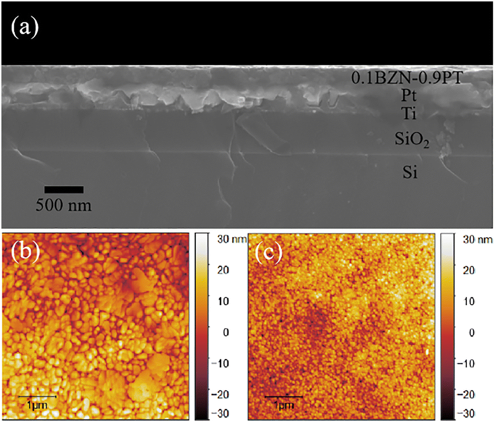 | ||
| Fig. 2 (a) Cross-sectional SEM image of the 0.1BZN–0.9PT thin films, AFM images of (b) PbTiO3 and (c) 0.1BZN–0.9PT thin films. | ||
To investigate the ferroelectric properties of the pure PT and 0.1BZN–0.9PT thin films, we conducted typical ferroelectric polarization versus electric field (P–E) loop measurements under different electric fields, as shown in Fig. 3. The P–E loops of PT are rounded and broad even at low electric fields (Fig. 3a), suggesting the strong leakage current of pure PT thin films. In contrast, the 0.1BZN–0.9PT film exhibits slender P–E loops, indicating the high quality of the thin films. Moreover, the 0.1BZN–0.9PT thin films exhibit a trend toward saturation as the electric field increases (Fig. 3b). However, applying an electric field exceeding 1200 kV cm−1 leads to significant leakage current and potential film breakdown. Therefore, we measured the P–E loops at the maximum electric field that the films can withstand. As shown in Fig. 3b, the 0.1BZN–0.9PT thin films demonstrate a large remanent polarization (Pr) value of 2Pr ≈ 174 μC cm−2 and a coercive field (EC) of approximately 275 kV cm−1. The two peaks in the current versus electric field curves are due to the polarization-switching current. It is proposed that typical P–E loops consist of three primary contributions: switching current, dielectric displacement current, and leakage current.40,41 The dielectric current corresponds to the capacitive component of the signal, while the leakage current arises from oxide vacancies and other defect movements within the film.40 To further understand the leakage behavior, we measured the leakage current of the thin films, as presented in Fig. S3. The introduction of BZN significantly reduced the leakage current from 8.7 × 10⁻³ A cm−2 for pure PT thin films to 2.7 × 10⁻⁶ A cm−2 for the 0.1BZN–0.9PT thin films. Here the leakage current of pristine PT thin films is comparable to a previous study.42 To obtain the intrinsic ferroelectric polarization, we employed the positive-up negative-down (PUND) pulse method43 to measure the P–E loops of 0.1BZN–0.9PT thin films (Fig. 3c). The PUND method effectively minimizes the contributions of dielectric current and leakage current, allowing us to isolate the intrinsic remanent polarization.41 From the PUND measurements, a large 2Pr value of approximately 118 μC cm−2 was observed, with an EC of about 336 kV cm−1. For comparison, the Pr value reported here is much higher than those of most BiMeO3–PbTiO3 thin films (Table S1). However, the Pr of 0.1BZN–0.9PT thin films is still lower than that of the Al0.8Sc0.2N thin films, which show a large Pr of approximately 135 μC cm−2 prepared by dual-source radio frequency reaction magnetron sputtering.44–46 Note that the relatively high EC observed in this study can be attributed to the small grain size and the large c/a ratio. Generally, the c/a ratio significantly influences domain switching behavior.43,47 A higher c/a value corresponds to greater lattice distortion, which suppresses the nucleation of new domains due to increased elastic energy within the domain walls.48 Consequently, a high EC is typically accompanied by a large c/a ratio.46 The robust ferroelectric polarization of the present 0.1BZN–0.9PT thin films can be attributed to their relatively large c/a ratio and uniform microstructure. The large c/a ratio is closely associated with the large PS displacement, which is the fundamental origin of ferroelectric polarization.49,50
 | ||
| Fig. 3 (a) Ferroelectric hysteresis P–E loops for the PT thin films, (b) ferroelectric hysteresis P–E loops and switching currents for the 0.1BZN–0.9PT thin films, and (c) ferroelectric hysteresis P–E loops for the 0.1BZN–0.9PT thin films in the PUND mode. | ||
Since the 0.1BZN–0.9PT thin films exhibit large ferroelectric polarization, TC is another critical parameter for high-performance ferroelectric materials. To determine the TC, we measured the dielectric permittivity (εr) and loss (tanδ) as a function of temperature at different frequencies, as shown in Fig. 4(a) and (b), respectively. The dielectric peak of the 0.1BZN–0.9PT thin films occurs at approximately 468 °C, corresponding to the ferroelectric-to-paraelectric phase transition, that is, TC.51 It is important to note that the phase transition occurs over a wide temperature range at higher frequencies. The εr value should be interpreted with caution, as they may be easily affected by probe vibration caused by thermal expansion during the measurements. Therefore, we did not show the dielectric permittivity. However, the phase transition temperature should be reliable, since it only depends on temperature. To further confirm the TC, we also conducted temperature-dependent XRD experiments on the 0.1BZN–0.9PT thin films, as shown in Fig. S2a. Additionally, to investigate the phase transition and accurately determine the TC, we performed a detailed analysis of the (100) diffraction peak by peak fitting, as presented in Fig. S2b. At low temperatures, the peak around 22.5° exhibits asymmetry and can be well fitted by two peaks corresponding to the (001) and (100) planes, indicating a tetragonal structure. However, as the temperature approaches the TC, the peak gradually becomes symmetric. The detailed lattice constants as a function of temperature are presented in Fig. S2c. It can be seen that the phase transition temperature (TC) is approximately 500 °C. Note that the TC determined by dielectric measurements is lower than that determined by temperature-dependent XRD data. One possible reason for this discrepancy may be the different accuracy of sample temperatures during dielectric and temperature-dependent XRD measurements. Additionally, XRD measurements usually require a certain degree of lattice distortion to detect structural changes, and a clear signal can only be observed when the phase transition is completed.52 Therefore, the measured TC is more representative of the end temperature of the phase transition. In contrast, dielectric measurements are particularly sensitive to local polarization changes. Even if the structure has not fully transformed, as long as there is a significant anomaly in the polarization response, the TC can be detected.53,54 Therefore, the TC measured by the dielectric constant method is likely to be slightly lower than that measured by temperature-dependent XRD experiments. The TC of the thin film is about 468 °C, suggesting its potential to work under high-temperature conditions.
 | ||
| Fig. 4 (a) Temperature dependent dielectric constant and (b) dielectric loss of the BZN–PT thin films. | ||
To further understand the enhanced ferroelectric properties in the present 0.1BZN–0.9PT thin films, we conducted comprehensive ab initio simulations. Since electric polarization arises from both ionic and electronic contributions, we first optimized the crystal structure. The resulting atomic positions in the A–O and B–O planes are shown in Fig. 5. At the B-site, the average displacements of Ti, Nb, and Zn along the z-axis were found to be 0.20 Å, 0.26 Å, and 0.05 Å, respectively. These results indicate that the substitution of Nb for Ti at the B-site slightly enhances the electric polarization. At the A-site, Pb atoms remain largely centrosymmetric, with an average displacement of 0.07 Å. In contrast, the doped Bi atom exhibits a noticeable deviation, with a displacement of 0.18 Å, thereby contributing additional ionic polarization to the total electric polarization. To analyze the electronic contribution, we examined charge redistribution and asymmetric bonding interactions, which can be visualized using the electron localization function (ELF). Focusing on the B-site, we compared the bonding between Ti–O and Nb/Zn–O. Unlike the nearly pure ionic interaction between Ti and O (represented by the blue region in the ELF), the substituted Nb atom not only introduces more electrons into the system but also forms a more pronounced covalent bond with one of the nearest oxygen atoms, as shown in Fig. 5(b). This asymmetric charge redistribution provides the system with an additional degree of freedom for electric polarization, thereby enhancing the polarization value. Similarly, Zn substitution also contributes to the system's polarization, though the effect is much smaller and relatively insignificant compared to Nb, as illustrated by the cyan region around the Zn atom. At the A-site, the substitution of Bi results in an enlarged green area in the ELF, indicating increased electron sharing in the Bi–O bond and thus an enhanced covalent interaction.
 | ||
| Fig. 5 Calculated electron localization function (ELF) and optimized crystal structure of 0.1BZN–0.9PT on (a) the ac plane and (b) the bc plane. The ELF values (0 to 1) are mapped on a blue-green-red color scale indicated on the right side. | ||
Through Bader charge analysis, we can quantitatively elucidate the remarkable polarization enhancement resulting from Nb substitution. The calculated Bader charge on the Ti atom is 1.92 e, exhibiting a deviation of 2.08 e from its ideal 4+ charge state. This deviation signifies the quantity of charge that does not contribute to ionic bond formation. Notably, the calculated Bader charge on Nb atoms is 2.68 e, which is 2.32 e lower than the ideal 5+ charge state. This pronounced deviation strongly suggests a significant decrease in the ionic character, thereby indicating a stronger covalent interaction between Nb and O atoms.
Conclusions
In summary, 0.1Bi(Zn2/3Nb1/3)O3–0.9PbTiO3 perovskite-type thin films were successfully fabricated via a conventional sol–gel method. Microstructural characterization reveals that the present thin films exhibit a homogeneous and dense morphology. Notably, the ferroelectric polarization properties are outstanding: the remanent polarization (2Pr) values measured in the normal mode and the PUND mode reach approximately 174 and 118 μC cm−2, respectively. Moreover, the 0.1Bi(Zn2/3Nb1/3)O3–0.9PbTiO3 thin films possess a high Curie temperature (TC) and a low leakage current. First-principles calculations demonstrate that the strong covalent interactions stemming from the hybridization of Pb/Bi–O and Ti/Zn/Nb–O bonds are responsible for the large ferroelectric polarization and elevated TC. The excellent overall ferroelectric performance of the present thin films suggests that these films should be of interest for FeRAM applications.Author contributions
Mengqi Ye: conceptualization, data curation, formal analysis, methodology, writing – original draft, writing – review & editing. Jin Liu: data curation, formal analysis, writing – original draft, writing – review & editing. Duo Wang: formal analysis, methodology, software, writing – original draft, writing – review & editing. Zhao Pan: conceptualization, data curation, formal analysis, funding acquisition, investigation, methodology, project administration, supervision, writing – original draft, writing – review & editing. Fengyi Zhou: software, writing – review & editing. Xubin Ye: data curation. Huajie Luo: data curation. Nianpeng Lu: data curation, writing – review & editing. Yunzhong Chen: data curation, writing – review & editing. Ruilong Wang: supervision, writing – review & editing. Youwen Long: funding acquisition, supervision, writing – review & editing.Conflicts of interest
There are no conflicts of interest to declare.Data availability
All the data have been included in the article.Supplementary information (SI): Fig. S1–S3 showing the HAADF image, temperature dependence of XRD patterns, and the leakage current density curves of the 0.1BZN–0.9PT thin films. See DOI: https://doi.org/10.1039/d5cp02016f.
Acknowledgements
We thank Dr Yunxiang Yang and Prof. Ying Zhang for the FIB sampling, and Prof. Xi Shen and Prof. Richeng Yu for the TEM experiments. This work was supported by the National Key R&D Program of China (Grant No. 2021YFA1400300), the National Natural Science Foundation of China (22271309, 12425403, 12304268, 11921004, and 12261131499), and the China Postdoctoral Science Foundation (Grant No. 2023M743741). Duo Wang acknowledges financial support from the Science and Technology Development Fund, Macau SAR (Grant No. 0062/2023/ITP2 and 0016/2025/RIA1), and Macao Polytechnic University (Grant No. RP/FCA-03/2023).References
- I. Vrejoiu, M. Alexe, D. Hesse and U. Gösele, Adv. Funct. Mater., 2008, 18, 3892–3906 CrossRef CAS.
- J. F. Scott, Science, 2007, 315, 954–959 CrossRef CAS PubMed.
- Y. L. Wang, H. Q. Zhao, L. X. Zhang, J. Chen and X. R. Xing, Phys. Chem. Chem. Phys., 2017, 19, 17493–17515 RSC.
- H. Ruan, T. G. Saunders, H. Giddens, H. Zhang, A. A. Ihalage, J. F. Kolb, M. Blunt, S. Haq, H. Yan and Y. Hao, J. Adv. Ceram., 2023, 12, 1521–1532 CrossRef CAS.
- Y. Yan, Z. Li, J. Li, H. Du, M. Zhang, D. Zhang and Y. Hao, ACS Appl. Mater. Interfaces, 2021, 13, 38517–38525 CrossRef CAS PubMed.
- G. Shirane, R. Pepinsky and B. C. Frazer, Acta Crystallogr., 1956, 9, 131–140 CrossRef CAS.
- R. E. Eitel, C. A. Randall, T. R. Shrout and S. E. Park, Jpn. J. Appl. Phys., 2002, 41, 2099–2104 CrossRef CAS.
- T. Yoshimura and S. Trolier-McKinstry, Appl. Phys. Lett., 2002, 81, 2065–2066 CrossRef CAS.
- J. Xiao, A. Wu, P. M. Vilarinho, A. R. Ramos and E. Alves, J. Mater. Chem., 2009, 19, 5572–5579 RSC.
- H. Wen, X. Wang, C. Zhong, L. Shu and L. Li, Appl. Phys. Lett., 2007, 90, 202902 CrossRef.
- G. Wu, H. Zhou, X. Zhou, N. Qin and D. Bao, J. Am. Ceram. Soc., 2010, 93, 925–927 CrossRef CAS.
- S. Zhang, R. E. Eitel, C. A. Randall, T. R. Shrout and E. F. Alberta, Appl. Phys. Lett., 2005, 86, 262904 CrossRef.
- G. A. Smolenskiĭ and I. E. Chupis, Phys.-Usp., 1982, 25, 475–493 CrossRef.
- J. Chen, K. Nittala, J. L. Jones, P. Hu and X. Xing, Appl. Phys. Lett., 2010, 96, 252908 CrossRef.
- M. R. Suchomel, A. M. Fogg, M. Allix, H. Niu, J. B. Claridge and M. J. Rosseinsky, Chem. Mater., 2006, 18, 4987–4989 CrossRef CAS.
- A. A. Belik, J. Solid State Chem., 2012, 195, 32–40 CrossRef CAS.
- L. Zhang, J. Chen, H. Zhao, L. Fan, Y. Rong, J. Deng, R. Yu and X. Xing, Dalton Trans., 2013, 42, 585–590 RSC.
- W. Song, G. Xi, Z. Pan, J. Liu, X. Ye, Z. Liu, X. Wang, P. Shan, L. Zhang, N. Lu, L. Fan, X. Qin and Y. Long, Chin. Phys. B, 2024, 33, 057701 CrossRef CAS.
- Z. Xie, B. Peng, J. Zhang, X. Zhang, Z. Yue and L. Li, J. Am. Ceram. Soc., 2015, 98, 2968–2971 CrossRef CAS.
- J. Kim, T. Onaya, H. R. Park, Y. C. Jung, D. N. Le, M. Lee, H. Hernandez-Arriaga, Y. G. Zhang, E. H. R. Tsai, C. Nam, T. Nabatame, S. J. Kim and J. Kim, ACS Appl. Electron. Mater., 2023, 5, 4726–4745 CrossRef CAS.
- Y. Yun, P. Buragohain, M. Li, Z. Ahmadi, Y. Z. Zhang, X. Li, H. L. Wang, J. Li, P. Lu, L. L. Tao, H. Y. Wang, J. E. Shield, E. Y. Tsymbal, A. Gruverman and X. S. Xu, Nat. Mater., 2022, 21, 903–909 CrossRef CAS PubMed.
- Y. L. Zhang, Q. X. Zhu, B. B. Tian and C. G. Duan, Nano-Micro Lett., 2024, 16, 227 CrossRef CAS PubMed.
- H. M. Qin, N. He, C. Han, M. C. Zhang, Y. Wang, R. Hu, J. W. Wu, W. J. Shao, M. Saadi, H. Zhang, Y. D. Hu, Y. Liu, X. P. Wang and Y. Tong, Nanomaterials, 2024, 14(11), 986 CrossRef CAS PubMed.
- R. Yu, H. Hojo, K. Oka, T. Watanuki, A. Machida, K. Shimizu, K. Nakano and M. Azuma, Chem. Mater., 2015, 27, 2012–2017 CrossRef CAS.
- Z. Pan, J. Chen, L. Fan, Y. Rong, S. Zheng, L. Liu, L. Fang and X. Xing, Mater. Res. Express, 2014, 1, 046301 CrossRef CAS.
- S. Chu, T. Chen, I. Tsai and W. Water, Sens. Actuators, 2004, 113, 198–203 CrossRef CAS.
- W. Gong, J. F. Li, X. Chu, Z. Gui and L. Li, Acta Mater., 2004, 52, 2787–2793 CrossRef CAS.
- C. Zhong, X. Wang, Y. Wu and L. Li, J. Am. Ceram. Soc., 2010, 93, 3993–3996 CrossRef CAS.
- C. Zhong, X. Wang, L. Guo and L. Li, Thin Solid Films, 2015, 580, 52–55 CrossRef CAS.
- G. Kresse and J. Furthmüller, Phys. Rev. B: Condens. Matter Mater. Phys., 1996, 54, 11169–11186 CrossRef CAS PubMed.
- J. P. Perdew, K. Burke and M. Ernzerhof, Phys. Rev. Lett., 1996, 77, 3865–3868 CrossRef CAS PubMed.
- W. Kohn and L. J. Sham, Phys. Rev. B: Condens. Matter Mater. Phys., 1965, 140, A1133–A1138 CrossRef.
- A. Savin, R. Nesper, S. Wengert and T. F. Fässler, Angew. Chem., Int. Ed. Engl., 1997, 36, 1808–1832 CrossRef CAS.
- G. Henkelman, A. Arnaldsson and H. Jónsson, Comput. Mater. Sci., 2006, 36, 354–360 CrossRef.
- E. K. Akdogan, C. J. Rawn, W. D. Porter and E. A. Payzant, J. Appl. Phys., 2005, 97, 084305 CrossRef.
- B. Jiang, J. L. Peng, L. A. Bursill and W. L. Zhong, J. Appl. Phys., 2000, 87, 3462–3467 CrossRef CAS.
- T. Ohno, D. Suzuki, K. Ishikawa and H. Suzuki, Adv. Powder Technol., 2007, 18, 579–589 CrossRef CAS.
- N. J. Lóh, L. Simão, C. A. Faller, A. De Noni and O. R. K. Montedo, Ceram. Int., 2016, 42, 12556–12572 CrossRef.
- K. R. Kambale, A. Mahajan and S. P. Butee, Met. Powder Rep., 2021, 74, 130–136 CrossRef.
- S. Martin, N. Baboux, D. Albertini and B. Gautier, Ultramicroscopy, 2017, 172, 47–51 CrossRef CAS PubMed.
- S. Martin, N. Baboux, D. Albertini and B. Gautier, Rev. Sci. Instrum., 2017, 88, 023901 CrossRef PubMed.
- X. W. Jiang, Q. Yang and J. X. Ca, Phys. Lett. A, 2016, 380, 1071–1074 CrossRef CAS.
- J. F. Scott, L. Kammerdiner, M. Parris, S. Traynor, V. Ottenbacher, A. Shawabkeh and W. F. Oliver, J. Appl. Phys., 1988, 64, 787–792 CrossRef CAS.
- X. Shi, Y. Chen, W. Shi and L. Wang, Seventh International Conference on Thin Film Physics and Applications, 2011, Proceedings, vol. 7995, 79951N.
- S. Yasuoka, R. Mizutani, R. Ota, T. A. Shiraishi, T. Shimizu, S. Yasui, Y. Ehara, K. Nishida, M. Uehara, H. Yamada, M. Akiyama, Y. Imai, O. Sakata and H. Funakubo, J. Ceram. Soc. Jpn., 2022, 130, 436–441 CrossRef CAS.
- Y. Zhang, Q. Zhu, B. Tian and C. Duan, Nano-Micro Lett., 2024, 16, 227 CrossRef CAS PubMed.
- T. Leist, T. Granzow, W. Jo and J. Rödel, J. Appl. Phys., 2010, 108, 014103 CrossRef.
- Y. H. Shin, I. Grinberg, I. W. Chen and M. R. Andrew, Nature, 2007, 449, 881–884 CrossRef CAS PubMed.
- Z. Pan, J. Chen, L. Fan, H. Liu, L. Zhang, L. Hu, Y. Ren, L. Liu, L. Fang, X. A. Fan, Y. W. Li and X. R. Xing, Inorg. Chem. Front., 2017, 4, 1352–1355 RSC.
- Z. Pan, J. Chen, R. Yu, L. Patra, P. Ravindran, A. Sanson, R. Milazzo, A. Carnera, L. Hu, L. Wang, H. Yamamoto, Y. Ren, Q. Z. Huang, Y. Sakai, T. Nishikubo, T. Ogata, X. A. Fan, Y. W. Li, G. Q. Li, H. Hojo, M. Azuma and X. R. Xing, Chem. Mater., 2019, 31, 1296–1303 CrossRef CAS PubMed.
- L. J. Liu, S. K. Ren, J. Zhang, B. L. Peng, L. Fang and D. W. Wang, J. Am. Ceram. Soc., 2018, 101, 2408–2416 CrossRef CAS.
- S. Dolabella, A. Borzì, A. Dommann and A. Neels, Small Methods, 2022, 6, 2100932 CrossRef CAS PubMed.
- Z. J. Jiang, B. Xu, S. Prosandeev, Y. Nahas, S. Prokhorenko, J. Íñiguez and L. Bellaiche, Phys. Rev. B, 2021, 103, L100102 CrossRef CAS.
- X. R. Wang, H. F. Guo, C. Zhou and J. K. Bai, Biomed. Eng., 2021, 20, 86 Search PubMed.
Footnote |
| † These authors contributed equally to this work. |
| This journal is © the Owner Societies 2025 |