
 Open Access Article
 This Open Access Article is licensed under a Creative Commons Attribution-Non Commercial 3.0 Unported Licence
Optically anisotropic ZnO nanorings fabricated using near-field photoelectrochemistry†
Yuki
Oba
,
Seung Hyuk
Lee
 and
Tetsu
Tatsuma
*
and
Tetsu
Tatsuma
*
Institute of Industrial Science, The University of Tokyo Komaba, Meguro-ku, Tokyo 153-8505, Japan. E-mail: tatsuma@iis.u-tokyo.ac.jp
First published on 5th May 2025
Abstract
Photonic nanofabrication based on optical near-field generation around nanostructures is a powerful technique for shaping materials at the nanoscale beyond the diffraction limit of light. Recently, we reported that not only localized surface plasmon resonance of metal nanoparticles but also the Mie resonance of photocatalytic semiconductor nanoparticles enables nanofabrication through site-selective excitation via an optical near field and reductive metal deposition at resonance sites. In the present study, we describe the self-etching of ZnO nanoplates in a site-selective manner using holes generated at resonance sites under linearly polarized UV light. This allowed the nanoplates to be shaped into nanorings and exhibit optical anisotropy corresponding to light polarization.
Introduction
Nanofabrication is a technology that controls the morphology, orientation and configuration of materials at the nanoscale and has been applied to the assembly and development of functional materials and devices.1–3 Among the various nanofabrication methods,2–4 photonic nanofabrication based on an optical near field localized in the vicinity of nanopores and nanoparticles (NPs)5,6 shapes materials at the nanoscale via site-selective melting, etching and deposition through local heating or chemical reactions.7,8 Since photonic nanofabrication allows processing beyond the diffraction limit of light, it has been applied to anisotropic growth of metal NPs,9 selective introduction of cocatalysts to a photocatalyst,10 and fabrication of chiral NPs11 using localized surface plasmon resonance (LSPR).We recently reported that such photonic nanofabrication is possible not only using the LSPR of metal NPs but also using other optical resonance such as the Mie resonance of semiconductor NPs.12 Specifically, by irradiating semiconducting ZnO nanoplates with linearly polarized UV light, Ag+ ions were reduced to metallic Ag, which was deposited on ZnO nanoplates in a site-selective manner at sites where optical near fields are localized. This near-field photocatalysis occurs as follows: A semiconductor NP is irradiated with linearly polarized light, and the optical near field is localized at certain sites due to optical resonance. Then, electrons in the valence band of the semiconductor NP are excited to the conduction band, and the excited electrons cause reduction reactions. If the reaction occurs at resonance sites before delocalization, site-selective reduction occurs. Similarly, it is possible that the holes generated in the valence band drive site-selective oxidation. If the holes can also be utilized for site-selective reactions and photonic nanofabrication, it would open up opportunities for the development of novel nanomaterials and devices.
We therefore employed ZnO, which is commonly used as a photocatalyst, to assess the possibility of achieving site-selective oxidation through local etching of ZnO. In fact, it is known that ZnO undergoes self-oxidative photocatalytic dissolution under specific conditions.13–15 In the present study, we chemically synthesized ZnO nanoplates and performed partial etching of the nanoplates under linearly polarized UV light to shape them into ZnO nanorings that exhibit linear dichroism (LD) corresponding to light polarization.
Experimental
Synthesis of ZnO nanoplates
ZnO nanoplates were synthesized using a previously reported method.16 Zinc(II) acetate dihydrate (37.4 mg), indium(III) acetate (3.8 mg) and octanoic acid (61.3 μL) were dissolved in 1-octadecene (ODE, 2.5 mL) at 150 °C for 1 h under N2 flow. The gas phase of the reaction vessel was filled with N2 after degassing (at 110 °C for 30 min). Next, the temperature of the reaction vessel was raised to 300 °C. After a mixture of ODE and oleylamine (50![[thin space (1/6-em)]](https://www.rsc.org/images/entities/char_2009.gif) :50 vol%, 447.4 μL) was injected into the vessel, the temperature was lowered to 280 °C and maintained for 1 h. The synthesized ZnO nanoplates were centrifuged (2 min at 5500g) twice using a mixture of toluene and ethanol (1:10).
:50 vol%, 447.4 μL) was injected into the vessel, the temperature was lowered to 280 °C and maintained for 1 h. The synthesized ZnO nanoplates were centrifuged (2 min at 5500g) twice using a mixture of toluene and ethanol (1:10).
Site-selective etching of the ZnO nanoplates
The synthesized ZnO nanoplates were redispersed in toluene (1 mL) and spin-coated (2000 rpm, 30 s) onto a glass substrate or a substrate coated with tin-doped indium oxide (ITO) for SEM observation, followed by annealing at 500 °C for 2 h to remove the organic species present on the ZnO nanoplates. The substrate with the ZnO nanoplates was immersed in an aqueous solution containing 1 mM benzoquinone and irradiated with vertically polarized UV light (365 nm, 25 mW cm−2) for 30 min for photocatalytic self-etching of the ZnO nanoplates.Analysis
The nanoplates on the glass plate before and after light irradiation were subjected to X-ray diffraction (XRD) analysis (SmartLab, Rigaku), atomic force microscopy (AFM) (NanoNavi/SPA400, Hitachi High-Tech), UV-visible-NIR absorption spectroscopy (V-670, Jasco) and X-ray photoelectron spectroscopy (XPS) (Phi Quantera SXM, Ulvac-Phi). Scanning electron microscopy (SEM) images were recorded using a field emission scanning electron microscope (JSM-7500FA, JEOL) equipped with an energy dispersive X-ray spectroscopy (EDS) probe. LD spectra were collected using a CD spectrophotometer (J-1700, Jasco).Results and discussion
Oxidative dissolution of the ZnO nanoplates
Wurtzite ZnO nanoplates were synthesized and loaded onto a solid substrate. It was confirmed from the SEM images (Fig. 1a) and AFM images (Fig. S1a) that the synthesized ZnO had a hexagonal shape with a width of 112 ± 19 nm (n = 100, the size distribution is shown in Fig. S1b, ESI†) and a thickness of 25 ± 5 nm (n = 30, Fig. S1c, ESI†). Nanoplates of this size were selected because if smaller, no significant resonance is obtained in the appropriate wavelength range, and if larger, the electric field distribution becomes too complex to analyse (Fig. S2, ESI†). For photoelectrochemical reactions, the substrate with ZnO nanoplates was immersed in a solution containing 1 mM benzoquinone and irradiated from the backside with vertically polarized UV light (365 nm, 25 mW cm−2) for 30 min, as illustrated in Fig. 1b. Difference spectrum for nonpolarized light absorption after the light irradiation was measured using an integrating sphere (Fig. 1c). The decrease in the UV absorption, which is assigned to the interband excitation of ZnO, reflects the partial dissolution of ZnO.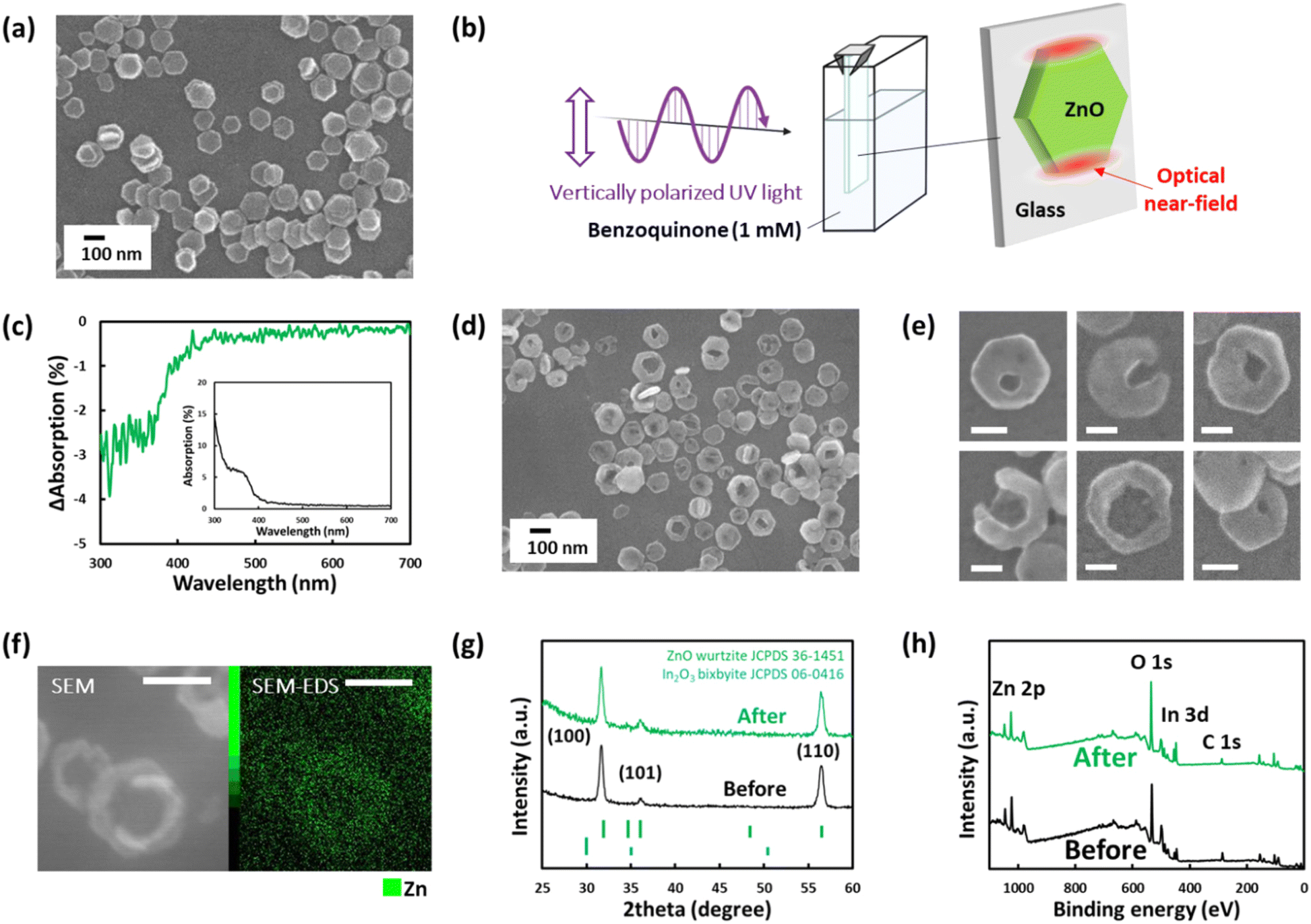 | ||
| Fig. 1 (a) Typical SEM image of the ZnO nanoplates on an ITO-coated glass substrate. (b) Illustration of the experimental setup for photoelectrochemical reactions. (c) Difference absorption spectrum of the ZnO nanoplates after irradiation with linearly polarized UV light. Inset shows a spectrum of the nanoplates before irradiation. Typical (d) and (e) SEM image of the ZnO nanoplates on a glass substrate, and (f) SEM-EDS image of the ZnO nanoplates on an ITO-coated glass substrate after polarized UV light irradiation. (g) In-plane XRD pattern and (h) XPS spectrum of the ZnO nanoplates before and after polarized UV light irradiation. | ||
Under UV irradiation, electrons are excited from the ZnO valence band to the conductive band, and the holes thus generated in the valence band (h+) are used for the following reaction, resulting in the dissolution of ZnO.17
| 2ZnO + 4h+ → 2Zn2+ + O2 | (1) |
The excited electrons in the conduction band (e−) are consumed by reduction of benzoquinone in the solution to hydroquinone as follows:
| C6H4O2 + 2H2O + 2e− → C6H6O2 + 2OH− | (2) |
As shown in the SEM and SEM-EDS images (Fig. 1d–f), nanoholes were formed after the irradiation in most of the ZnO nanoplates, resulting in the formation of nanorings. In some cases, the nanoholes reached the edge of each ZnO nanoplate and split nanorings were formed. No significant change such as segregation of In2O3 was seen in the XRD pattern (Fig. 1g) or XPS survey scan spectrum (Fig. 1h) after UV light irradiation. Although the XPS narrow scan spectra for Zn 2p, In 3d and O 1s (Fig. S3a–c, ESI†) showed a slight shift in the Zn 2p peak to lower binding energy, broadening of the In 3d peak and an increase in the OH-based O 1s signal at ∼533 eV, these changes are reasonably attributed to surface modifications due to ZnO dissolution rather than to changes in bulk composition. We therefore conclude that the nanorings almost completely retained their crystal structure and compositions during the photocatalytic process.
Optical anisotropy of the ZnO nanoplates
Since the self-oxidative dissolution of the ZnO nanoplates was caused by linearly polarized UV light, it is possible that the NPs gain optical anisotropy as a result of the dissolution. We therefore examined the LD properties of the ZnO nanoplates (Fig. 2a). Before UV light irradiation, the sample showed no significant LD signals. However, a positive LD signal was observed in the UV range after irradiation with vertically polarized UV light in the benzoquinone solution for 15 or 30 min. A positive signal indicates that extinction of horizontally polarized light is stronger than that of the vertically polarized light. This wavelength region matches the region where the ZnO nanoplates show optical absorption (Fig. 1c, inset). Therefore, the LD signal stems from the dissolution of the ZnO nanoplates.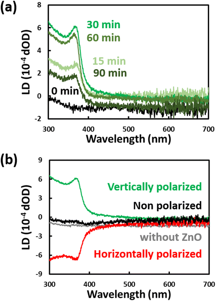 | ||
| Fig. 2 (a) LD spectra of the ZnO nanoplates on a glass plate after irradiation with vertically polarized UV light (0–90 min) in a 1 mM benzoquinone solution. (b) LD spectra of the ZnO nanoplates after irradiation with vertically polarized, horizontally polarized and non-polarized UV light (30 min), and LD spectrum of the substrate without ZnO after irradiation with vertically polarized UV light. | ||
As the irradiation time was extended from 15 to 30 min, LD signal intensity increased. The LD signal was inverted to negative when the ZnO nanoplates were irradiated with horizontally polarized UV light instead of vertically polarized light (Fig. 2b). The LD signal was almost negligible when non-polarized light was used. In addition, the LD signal was negligible when a substrate without the ZnO nanoplates was irradiated with vertically polarized UV light. Further irradiation for 60 min or longer resulted in a decrease in the LD signal because of over-dissolution of the nanoplates, as reflected by the significantly decreased extinction (Fig. S4, ESI†). From these results, it was confirmed that the LD signals originated from the linearly polarized UV light irradiation of the ZnO nanoplates.
Statistical analysis of nanohole geometry
Next, we studied the statistics of the geometry of the nanoholes formed by irradiating with vertically polarized light for 30 min. The distance d between the ZnO nanoplate and nanohole centres, the angle θ between the vertical line indicating the polarization direction and a line connecting the nanoplate and nanohole centres and the horizontal and vertical lengths of the nanohole a and b, respectively, were evaluated for 100 randomly picked nanoplates containing a nanohole, as described in the ESI† (page 3 and Fig. S5). Nanoholes formed by nonpolarized light were also subjected to analysis (75 nanoplates). SEM images used for the analysis are shown in Fig. S6 and S7 (ESI†).The data are summarized in Fig. 3 and Fig. S8 (ESI†). The polar histograms in Fig. 3a and Fig. S8a (ESI†) show that the nanoholes formed by the vertically polarized light tend to be distributed vertically. The trend for the nanoholes formed by the polarized light is similar to the distribution of the optical near field around the nanoplate shown in Fig. 3b. The reasons why the nanoholes are preferentially formed on the (002) facets while the near field is localized at the edges are addressed in the section discussing the mechanism (see below).
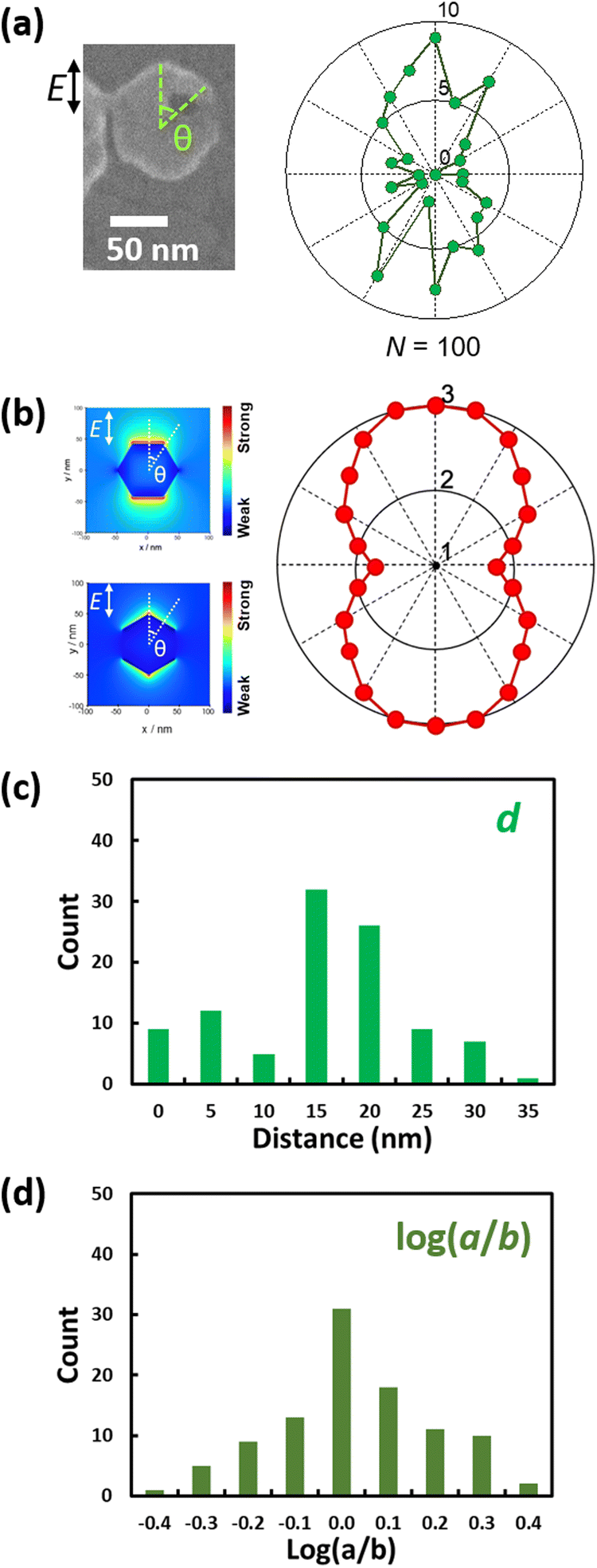 | ||
| Fig. 3 Statistical data for ZnO nanorings prepared through vertically polarized UV light irradiation. (a) Polar histogram for the angle θ of the nanohole position. (b) Polar diagram for the intensity of the optical near field around the nanoplate under vertically polarized light. Histograms of geometric parameters (c) d and (d) log(a/b). | ||
The data for d are summarized in Fig. 3c. In addition, the a, b, 0.25πab and log(a/b) values are summarized in Fig. 3d and Fig. S6b, c (ESI†). The averaged aspect ratio a/b was 1.11 and 1.00 for samples prepared with vertically polarized and nonpolarized light, respectively. Horizontal ellipses predominate over vertical ones for the nanoholes prepared via vertically polarized light irradiation.
Simulation of the LD spectra
On the basis of the statistical data, we simulated the LD spectra of the ZnO nanorings using the FDTD method. The simulation model, shown in Fig. 4a, is based on round disks instead of hexagonal nanoplates with different orientations to eliminate possible influences of the orientation.12 The nanoholes are also approximated with elliptical ones, although the experimentally obtained nanoholes are not perfectly elliptical. Elliptic and rhombus nanoholes with the same area and aspect ratio lead to quite similar LD spectra, as shown in Fig. S9 (ESI†), indicating that it is a good approximation. The diameter of the nanodisk is 91 nm, which is the diameter of the disk with an area equal to that of a 100 nm wide hexagon. The thickness of the model is 19 nm, which is the value obtained through AFM analysis. We selected the dielectric function for ZnO reported by Stelling et al.,18 which gives the best-fit spectra. The values of parameters d, a and b are 15.0, 29.1 and 26.1, respectively, which are the average values obtained by the experiments with 30-min UV irradiation. The simulated LD spectrum is shown in Fig. 4b (red) and is in good agreement with the experimentally obtained spectrum shown in Fig. 2a.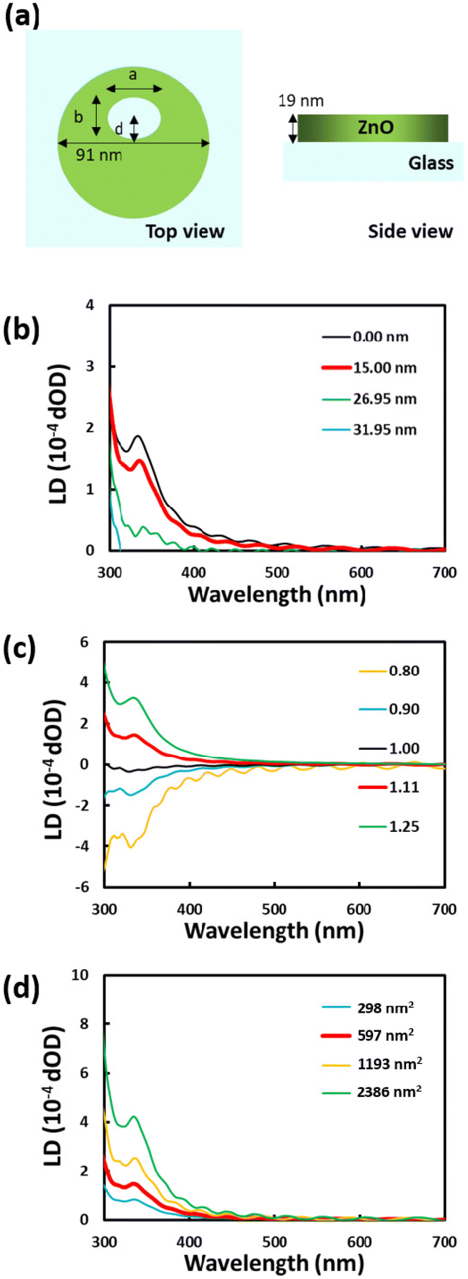 | ||
| Fig. 4 (a) Model of a ZnO nanoring for FDTD calculations. Calculated LD spectra with varied (b) d, (c) a/b and (d) 0.25πab. Parameter d = 15.0 nm, a = 29.1 nm and b = 26.1 nm. | ||
Next, the influence of each parameter of the calculation model on the LD spectrum was examined. Either d, a/b (nanohole ellipticity) and 0.25πab (nanohole area) was changed, and the other parameters were kept unchanged. When the d value was 0, the nanoring with an elliptic nanohole (i.e., a/b = 1.11) at the nanoplate center exhibited a positive LD signal (Fig. 4b). As the d value increased to 31.95 nm, at which point the nanohole edge was in contact with the ZnO edge, the LD signal weakened gradually. Alternatively, when the nanohole was not elliptical but perfectly circular (i.e., a/b = 1, log(a/b) = 0), the nanoring showed negligible LD signal, even if the nanohole was off the centre of the disk (d = 15.0). As the a/b value increased, the nanoring exhibited a positive LD signal, and it increased gradually (Fig. 4c). Conversely, a negative LD signal increased with a decreasing a/b value.
These simulation results lead to the conclusion that the anisotropy of the nanohole primarily governs the LD signal and its sign, and the position of the nanohole mainly affects the signal intensity. The area of the nanohole (0.25πab) also affects the signal intensity: the signal is enhanced as the nanohole area increases from 298 to 2386 nm2 (Fig. 4d).
Mechanism of the near-field oxidation reaction
As illustrated in Fig. 5a, when a ZnO nanoplate is irradiated with linearly polarized UV light, the optical near field is localized according to the polarization direction. Under vertically polarized light, the near field is localized around the top and bottom edges, and under horizontally polarized light, the near field is localized around the left and right edges. The optical near field excites electrons in the ZnO valence band to the conduction band, and holes are generated in the valence band accordingly around the edges. | ||
| Fig. 5 Mechanisms of the localized and anisotropic etching of ZnO nanoplates. (a) Reaction sites under linearly polarized UV light. (b) Band structure of ZnO and migration of carriers. (c) Formation of an elliptic nanohole. | ||
However, corrosion occurred preferentially at the ZnO (002) facets rather than at the ZnO (100) facets at nanoplate edges. This trend can be explained if the (002) facets have a tendency to attract holes or to be more easily oxidized compared with the (100) facets. In actuality, it is known that the band levels of the (002) facets are higher or more negative in potential than those of the (100) facets, as shown in Fig. 5b.19 If this trend holds also for the present In-doped ZnO, electrons excited at the (100) facets at the edges would stay there and drive reduction reactions at the (100) facets, and the holes would tend to migrate from the (100) to the (002) facets and drive oxidation reactions there. Indeed, reductive deposition of Ag was observed mainly at the edges for the In-doped ZnO.12 In addition, because the (002) facet has a higher polarity than the (100) facet, the corrosion is more likely to occur at the (002) facet.20,21 Distribution of defects might also contribute to these trends.22 Thus, although the optical near field is stronger at the edges, the oxidation of ZnO (eqn (1)) occurs at sites on the (002) facets, close to the edges. This also explains why the nanoholes are off-centre.
Since the holes migrate from the top or bottom edge under vertically polarized light, horizontal growth is dominant for a nanohole, as shown in Fig. 5c. In addition, the optical near field around the nanohole in the horizontal direction is stronger than that in the vertical direction for circular and elliptical nanoholes (a/b = 0.8, 1.0 and 1.25), as shown in Fig. S10 (ESI†). This may also contribute to horizontal growth, although the near field intensity was much lower than that around the nanoplate edges. In either event, horizontal growth makes the nanoring exhibit a positive LD signal, as mentioned above.
Conclusions
The ZnO nanoplates were shaped into nanorings through self-oxidative dissolution by irradiating with linearly polarized UV light. After irradiation with vertically polarized UV light, the ZnO nanoplates showed a positive LD signal in the UV range, whereas irradiation with horizontally polarized UV light resulted in a negative LD signal. In the case of vertical polarization, the optical near field was localized in the vicinity of the upper and lower edges of the ZnO nanoplate. Excited electron–hole pairs were generated as a result of local excitation of ZnO by the optical near field; the holes then migrated from the (100) facets at the nanoplate edge to the (002) facets, and ZnO was etched by the holes to form nanoholes. The localized and anisotropic growth of the nanoholes led to optical anisotropy. Thus, it was demonstrated that not only reduction but also oxidation can be driven in a site-selective manner through near-field photoelectrochemistry of semiconductor NPs. This technique can be applied to sophisticated and convenient shaping of semiconductor NPs.Author contributions
Y. Oba: investigation; writing – original draft. S. H. Lee: conceptualization; investigation; writing – original draft. T. Tatsuma: conceptualization; funding acquisition; supervision; writing – review & editing.Data availability
The data supporting the findings of this study are included in the article and ESI.†Conflicts of interest
There are no conflicts to declare.Acknowledgements
This work was supported in part by a Grant-in-Aid for Scientific Research (A) (no. JP20H00325) from the Japan Society for the Promotion of Science (JSPS) and the Advanced Research Infrastructure for Materials and Nanotechnology in Japan (ARIM) of the Ministry of Education, Culture, Sports, Science and Technology (MEXT), grant number JPMXP1223UT0282.Notes and references
- J. A. Schuller, E. S. Barnard, W. Cai, Y. C. Jun, J. S. White and M. L. Brongersma, Nat. Mater., 2010, 9, 193–204 CrossRef CAS.
- A. Biswas, I. S. Bayer, A. S. Biris, T. Wang, E. Dervishi and F. Faupel, Adv. Colloid Interface Sci., 2012, 170, 2–27 CrossRef CAS.
- S. Kasani, K. Curtin and N. Wu, Nanophotonics, 2019, 8, 2065–2089 CrossRef CAS.
- H.-D. Yu, M. D. Regulacio, E. Ye and M.-Y. Han, Chem. Soc. Rev., 2013, 42, 6006 RSC.
- S. Link and M. A. El-Sayed, J. Phys. Chem. B, 1999, 103, 8410–8426 CrossRef CAS.
- R. Jin, Y. Cao, C. A. Mirkin, K. L. Kelly, G. C. Schatz and J. G. Zheng, Science, 2001, 294, 1901–1903 CrossRef CAS.
- D. G. Schauer, J. Bredehoeft, U. Yunusa, A. Pattammattel, H. J. Wörner and E. A. Sprague-Klein, Phys. Chem. Chem. Phys., 2024, 26, 25581–25589 RSC.
- C. Zhan, J. Yi, S. Hu, X. G. Zhang, D. Y. Wu and Z. Q. Tian, Nat. Rev. Methods Primers, 2023, 3, 12 CrossRef CAS.
- K. Saito and T. Tatsuma, Nanoscale, 2017, 9, 18624–18628 RSC.
- K. Kim, H. Nishi and T. Tatsuma, J. Chem. Phys., 2023, 157, 111101 CrossRef PubMed.
- K. Saito and T. Tatsuma, Nano Lett., 2018, 18, 3209–3212 CrossRef CAS.
- Y. Oba, S. H. Lee and T. Tatsuma, J. Phys. Chem. C, 2024, 128, 827–831 CrossRef CAS.
- J. Wu and D. Xue, Mater. Res. Bull., 2010, 45, 295–299 CrossRef CAS.
- S. Jung, W. Cho, H. J. Lee and M. Oh, Angew. Chem., 2009, 121, 1487–1490 CrossRef.
- K. Qi, J. Yang, J. Fu, G. Wang, L. Zhu, G. Liu and W. Zheng, CrystEngComm, 2013, 15, 6729–6735 RSC.
- S. Ghosh, M. Saha and S. K. De, Nanoscale, 2014, 6, 7039–7051 RSC.
- S. Chen, D. Huang, P. Xu, W. Xue, L. Lei, M. Cheng, R. Wang, X. Liu and R. Deng, J. Mater. Chem. A, 2020, 8, 2286–2322 RSC.
- C. Stelling, C. R. Singh, M. Karg, T. A. F. König, M. Thelakkat and M. Retsch, Sci. Rep., 2017, 7, 42530 CrossRef CAS.
- C. Tang, M. J. S. Spencer and A. S. Barnard, Phys. Chem. Chem. Phys., 2014, 16, 22139–22144 RSC.
- E. Palacios-Lidón, D. F. Pickup, P. S. Johnson, R. E. Ruther, R. Tena-Zaera, R. J. Hamers, J. Colchero, F. J. Himpsel, J. E. Ortega and C. Rogero, J. Phys. Chem. C, 2013, 117, 18414–18422 CrossRef.
- D. Xu, B. Chen, X. Ren, C. Han, Z. Chang, A. Pan and H. Zhou, Energy Environ. Sci., 2024, 17, 642–654 RSC.
- E. Debroye, J. V. Loon, H. Yuan, K. P. F. Janssen, Z. Lou, S. Kim, T. Majima and M. B. J. Roeffaers, J. Phys. Chem. Lett., 2017, 8, 340–346 CrossRef CAS PubMed.
Footnote |
| † Electronic supplementary information (ESI) available: Experimentally obtained spectra and SEM data, simulated spectra, near field distributions and statistically analysed data. See DOI: https://doi.org/10.1039/d5cp00753d |
| This journal is © the Owner Societies 2025 |