
 Open Access Article
 This Open Access Article is licensed under a Creative Commons Attribution-Non Commercial 3.0 Unported Licence
First principles investigation of electron mobility enhancement of β-Ga2O3 doped with indium†
Leng
Zhang
*ab,
Jiajian
Huang
b,
Yuhao
Shen
a,
Fei
Liu
b,
Pengzhan
Zhang
b,
Danbei
Wang
b,
Kongping
Wu
b and
Yaowei
Wei
c
aNational Laboratory of Solid State Microstructures and School of Physics, Nanjing University, Nanjing 210093, China. E-mail: zhangleng2018@jit.edu.cn
bSchool of Electronics and Information Engineering, Jinling Institute of Technology, Nanjing 211169, Jiangsu, P. R. China
cState Center for International Cooperation on Designer Low-Carbon & Environmental Materials (CDLCEM), School of Materials Science and Engineering, Zhengzhou University, Zhengzhou 450001, China
First published on 22nd January 2025
Abstract
β-Ga2O3 is one of the new-generation wide-bandgap semiconductor materials that has attracted much attention in recent years. However, the reported room-temperature electron mobility of β-Ga2O3 is much lower than GaN and SiC. Alloying Ga2O3 is expected to endow the material with superior carrier transport properties. Herein, we mainly investigate the electron mobility of pure Ga2O3, In-doped Ga2O3, and Al-doped Ga2O3 from first-principles considering acoustic deformation potential (ADP) scattering, polar optical phonon (POP) scattering and ionized impurity (IMP) scattering. The structure optimization, electronic band structure, and temperature-dependent and concentration-dependent electron mobility are investigated. The results show that the mobility of In–Ga2O3 is always the highest at 105–650 K, and POP scattering is the dominant factor limiting the electron mobility from 150–650 K. The mobility enhancement by In-doping is attributed to the smaller effective mass caused by the In 5s state despite its slightly increased electron–phonon coupling strength. The predicted electron mobilities for Ga2O3, Al–Ga2O3 and In–Ga2O3 at an electron concentration of 1.0 × 1017 cm−3 are 151.5 cm2 V−1 s−1, 137.8 cm2 V−1 s−1 and 184.9 cm2 V−1 s−1 at room temperature, respectively. This work provides an alternative route to enhance the electron mobility of Ga2O3 and guides in engineering their electronic transport properties for high-power electronics.
1. Introduction
Wide bandgap semiconductor materials, represented by gallium oxide (β-Ga2O3),1 aluminum nitride (AlN),2 and diamond,3 have become the most promising materials for the new generation of semiconductors. Their high bandgap (>4.5 eV)4 and high breakdown voltage (>1800 V)5,6 significantly expand the depth and breadth of applications in electronic and optical devices. β-Ga2O3 has gained market favor due to its high-quality substrates and large-scale substrate production capabilities,7 prompting in-depth exploration of performance optimization by the academic and commercial communities. In semiconductor devices, carrier transport properties are crucial as they determine the electrical performance. However, the reported room-temperature electron mobility of β-Ga2O3 remains below 200 cm2 V−1 s−1,8–12 which is 1 to 2 orders of magnitude lower than that of third-generation semiconductors like SiC, GaN, etc.,13,14 hindering the efficiency and application range of Ga2O3 devices. Alloying Ga2O3 is expected to endow the material with superior carrier transport properties.Existing research showed that doping could change the carrier mobility of semiconductors. Considering only acoustic phonon (rather than polar phonon) scattering, Zhang found that by doping with Cu and Sn, the electron mobility of Ga2O3 was enhanced significantly from 847 cm2 V−1 s−1 to 12![[thin space (1/6-em)]](https://www.rsc.org/images/entities/char_2009.gif) 409 cm2 V−1 s−1 and 4217 cm2 V−1 s−1,15 respectively. Focusing on a simplified model based on deformation potential scattering, Yu found that the electron mobility of Ga2O3 was reduced from intrinsic 283.8 cm2 V−1 s−1 to 207.7 cm2 V−1 s−1, 212.6 cm2 V−1 s−1, and 187.3 cm2 V−1 s−1 by doping with Si, Ge and Sn.16 Typically, the structure cells chosen for first principles calculation contain only several dozen atoms, in which even doping with one atom could result in heavy doping, leading to a band structure similar to that of metals or semimetals, when doping with elements that are not isoelectronic with Ga or O. In such cases, using a semiconductor model to calculate its electrical transport properties might not be accurate. Isoelectronic doping does not present this issue. Li calculated the impact of indium doping on the electrical properties of single-layer Ga2O3 metal–oxide–semiconductor field-effect transistors (MOSFETs) and discovered that the on-current for high-performance and low-power achieved great improvement at In doping concentrations of 5% and 20%.17 Using a chemical vapor deposition method, Tian found that In-doping enhanced the mobility of Ga2O3 nanobelts compared to pure Ga2O3, thereby improving the sensitivity and responsivity of Ga2O3 photodetectors,18 consistent with Ji's experimental results.19 Both theoretical and experimental studies have shown that the electron mobility of Ga2O3 could be improved by doping with indium. However, the scattering mechanisms in In-doped Ga2O3 have not been thoroughly studied yet. Moreover, literature has indicated that Al, which belongs to the same group as In, reduced the mobility when doped in Ga2O3.20,21 It is worth noting that these two elements belonging to the same group contribute to completely different effects on Ga2O3. Therefore, this research aims to compare various properties of In-doped Ga2O3, pure Ga2O3 and Al-doped Ga2O3, and then to investigate the reasons behind In-doping enhancing the mobility of Ga2O3.
409 cm2 V−1 s−1 and 4217 cm2 V−1 s−1,15 respectively. Focusing on a simplified model based on deformation potential scattering, Yu found that the electron mobility of Ga2O3 was reduced from intrinsic 283.8 cm2 V−1 s−1 to 207.7 cm2 V−1 s−1, 212.6 cm2 V−1 s−1, and 187.3 cm2 V−1 s−1 by doping with Si, Ge and Sn.16 Typically, the structure cells chosen for first principles calculation contain only several dozen atoms, in which even doping with one atom could result in heavy doping, leading to a band structure similar to that of metals or semimetals, when doping with elements that are not isoelectronic with Ga or O. In such cases, using a semiconductor model to calculate its electrical transport properties might not be accurate. Isoelectronic doping does not present this issue. Li calculated the impact of indium doping on the electrical properties of single-layer Ga2O3 metal–oxide–semiconductor field-effect transistors (MOSFETs) and discovered that the on-current for high-performance and low-power achieved great improvement at In doping concentrations of 5% and 20%.17 Using a chemical vapor deposition method, Tian found that In-doping enhanced the mobility of Ga2O3 nanobelts compared to pure Ga2O3, thereby improving the sensitivity and responsivity of Ga2O3 photodetectors,18 consistent with Ji's experimental results.19 Both theoretical and experimental studies have shown that the electron mobility of Ga2O3 could be improved by doping with indium. However, the scattering mechanisms in In-doped Ga2O3 have not been thoroughly studied yet. Moreover, literature has indicated that Al, which belongs to the same group as In, reduced the mobility when doped in Ga2O3.20,21 It is worth noting that these two elements belonging to the same group contribute to completely different effects on Ga2O3. Therefore, this research aims to compare various properties of In-doped Ga2O3, pure Ga2O3 and Al-doped Ga2O3, and then to investigate the reasons behind In-doping enhancing the mobility of Ga2O3.
In this work, we emphasize the scattering mechanisms determining the electron mobility of Ga2O3, In–Ga2O3, and Al–Ga2O3, taking acoustic deformation potential (ADP) scattering, polar optical phonon (POP) scattering and ionized impurity (IMP) scattering fully into account. We computed the band structures and density of states for three different structures, as well as the necessary parameters for ADP, POP and IMP scattering. Additionally, we calculated the variations in ADP, POP, and IMP scattering between 105 and 650 K and their respective contributions to the total mobility. Lastly, we investigated the mobility enhancement mechanism of In-doped Ga2O3.
2. Computational methodology
There are two kinds of unequal Ga atoms in the lattice structure of β-Ga2O3, namely GaI with tetrahedral coordination and GaII with octahedral coordination, as shown in Fig. 1. We have calculated the doping formation energy of In and Al atoms substituting for GaI and GaII, from which we could conclude that Al atoms preferentially substitute for GaII atoms, while In atoms preferentially substitute for GaI atoms. All the DFT calculations were performed in the 1 × 2 × 1 monoclinic Ga2O3 supercell using the Vienna ab initio simulation package (VASP) code.22,23 The generalized gradient approximation (GGA) involving the Perdew–Burke–Ernzerhof (PBE)24 functional was employed to describe the exchange correlation potential. The plane wave cutoff energy was set to 400 eV for all calculations. For the optimization and other property calculations, 3 × 6 × 7 and 4 × 7 × 8 Monkhorst–Pack k-points sampling were applied. These calculations were performed with 1 × 10⁻⁸ eV per atom energy tolerance and 0.01 eV Å−1 force tolerance. To counteract the underestimation on the band gaps of GGA, and reproduce the correct band-structure of β-Ga2O3, the Heyd–Scuseria–Ernzerhof (HSE06) screened hybrid functional25 was adopted to acquire the band structure as well, and the mixing parameter of 0.39 was set. | ||
| Fig. 1 Crystal structure of the Ga2O3 computational model. Green spheres represent cation antimony, and red spheres represent anion oxygen. | ||
Based on the momentum relaxation time approximation, the electron mobility, μe, can be computed through the linearized Boltzmann transport equation (BTE),26–29
 | (1) |
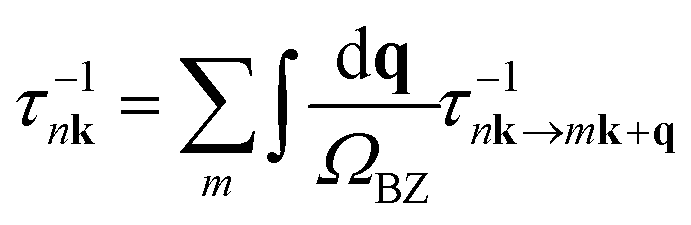 | (2) |
 | (3) |
For elastic scattering, the partial decay rate can be written as
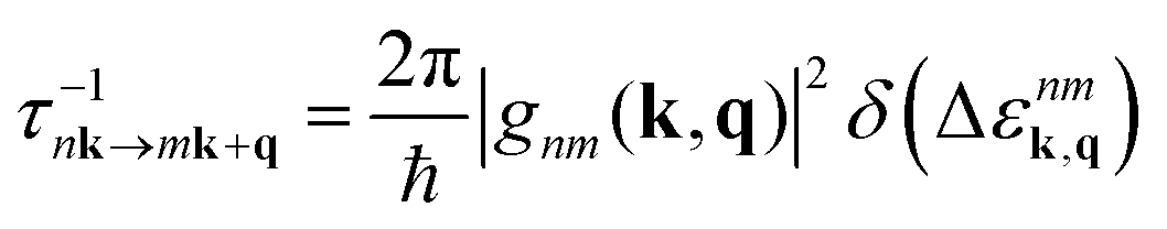 | (4) |
The scattering mechanisms of IMP33,34 and ADP35–38 belong to elastic scattering. The matrix elements for ADP, IMP and POP are calculated, respectively. Before the total mobility can be obtained, the basic parameters are calculated firstly. These include the ADP matrix parameters of the fully anisotropic acoustic deformation potential and elastic constants, POP matrix parameters including static (εs), high-frequency (ε∞) dielectric constants and effective phonon frequency (ωpo), etc. Through Fourier interpolation in the first Brillouin zone to compute electron mobility by AMSET,29 we can accurately evaluate the contribution of individual scattering mechanisms on a much-denser mesh of dimensions 13 × 25 × 27 after convergence tests.
3. Results and discussion
3.1. Electronic band structure
The lattice parameters of Ga2O3, Al–Ga2O3 and In–Ga2O3 are listed in Table 1. The calculated Ga2O3 lattice parameter results are in good agreement with the experimental data39 (deviation less than 1.8%) and previous calculations,40 demonstrating reliability of the employed theoretical methodology. Al–Ga2O3 has a slightly smaller lattice parameter, while In–Ga2O3 has a slightly larger lattice parameter, as Al atoms are smaller than Ga atoms while In atoms are larger than Ga atoms.To explore the differences in energy band, electronic occupancy states, and effective electron mass between pure Ga2O3 and doped Ga2O3, we performed calculations of the band structure, total density of states (TDOS), and partial density of states (PDOS). Fig. 2(a)–(c) present the electronic band structures of Ga2O3, Al–Ga2O3 and In–Ga2O3 with a Brillouin zone path of G–F–Q–Z–G calculated using PBE (orange lines) and HSE (blue lines), respectively. This reveals that the electronic band structures predicted using PBE and HSE demonstrate the same dispersion shape, except for the bandgap values, which means that they have the equivalent effective mass closely related to the curvature of the band at the high symmetry point. The band gap of Ga2O3 (Fig. 2a) obtained using HSE and PBE is 4.91 and 2.05 eV respectively. The gap between the bandgap calculated by HSE and the experimental results of 4.86 eV41 is very small. For Al–Ga2O3 (Fig. 2b), the band gap is 5.05 and 2.18 eV, respectively, while for In–Ga2O3 (Fig. 2c), the band gap is 4.77 and 1.93 eV, respectively. As HSE requires heavy computational resources, PBE is chosen to predict the carrier transport properties of these three Ga2O3 structures.
 | ||
| Fig. 2 Electronic band structures of pure Ga2O3, Al–Ga2O3, and In–Ga2O3 calculated using PBE (orange lines) and HSE (blue lines) functionals. | ||
In this study, we only focus on the electron mobility. From the band diagram, it can be seen that the conduction band minimum (CBM) is located at the gamma point. The electron effective mass  is defined as:
 | (5) |
![[k with combining right harpoon above (vector)]](https://www.rsc.org/images/entities/i_char_006b_20d1.gif) ) is the dispersion relationship for the n-th electronic band. Using the effective mass calculator (EMC)42 and finite difference method, we have calculated the effective mass at CBM, as shown in Table 2. The effective masses of pure Ga2O3 along x, y, and z are 0.22, 0.23, and 0.21, which are close to the values reported in the literature of 0.22, 0.22, and 0.21.40 The electron effective mass distributions reveal that the electron effective mass
) is the dispersion relationship for the n-th electronic band. Using the effective mass calculator (EMC)42 and finite difference method, we have calculated the effective mass at CBM, as shown in Table 2. The effective masses of pure Ga2O3 along x, y, and z are 0.22, 0.23, and 0.21, which are close to the values reported in the literature of 0.22, 0.22, and 0.21.40 The electron effective mass distributions reveal that the electron effective mass  is basically isotropic, consistent with the subsequent mobility calculations. The effective masses of Al–Ga2O3 are 0.24, 0.24, and 0.23, slightly higher than pure Ga2O3, which is unfavorable for carrier transport; meanwhile the effective masses of In–Ga2O3 are 0.21, 0.22, and 0.21, slightly lower than pure Ga2O3, which is beneficial for carrier transport.
| Structure | Electron effective mass
|
||
|---|---|---|---|
|
|
|
|
|
| Ga2O340 | 0.22 | 0.22 | 0.21 |
| Ga2O3 | 0.22 | 0.23 | 0.21 |
| Al–Ga2O3 | 0.24 | 0.24 | 0.23 |
| In–Ga2O3 | 0.21 | 0.22 | 0.21 |


The total density of states (TDOS) curves for pure Ga2O3, Al–Ga2O3, and In–Ga2O3 are similar, as shown in Fig. 3. Near the valence band maximum (VBM), the states are mainly contributed by O 2p and Ga 3p states. The O 2p states are localized below VBM, leading to a flat valence band, bringing about large hole effective mass. The DOS near the CBM is very low, resulting in a steep conduction band, meaning Ga2O3 has small electron effective mass. Al 3s and Al 3p states have minimal contribution to CBM as shown in Fig. 3(b) and (d). In contrast, In–Ga2O3 shows slightly higher In 5s states near the CBM (3.5–5 eV), resulting in a higher TDOS, as shown in Fig. 3(c) and (e). However, in the region that determines the electron effective mass at the CBM (1.93–2.05 eV for In–Ga2O3, 2.06–2.15 eV for Ga2O3, circled in red), the TDOS of In–Ga2O3 is the lowest caused main by the In 5s state, with less localization and a steeper CBM, resulting in a lower electron effective mass. The detailed TDOS of Ga2O3 and In–Ga2O3 near the CBM is shown in Table S1 (ESI†).
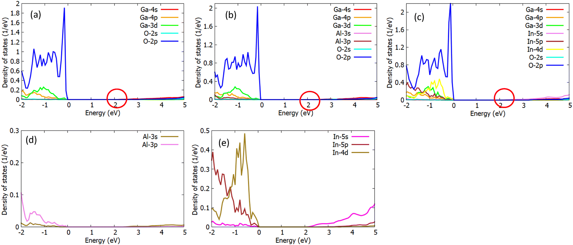 | ||
| Fig. 3 TDOS of pure Ga2O3 (a), Al–Ga2O3 (b), and In–Ga2O3 (c); PDOS of Al in Al–Ga2O3 (d) and PDOS of In in In–Ga2O3 (e). | ||
3.2. Electrical transport properties caused by ADP
Based on the electronic band structure, the scattering rate from ADP, POP, and IMP and the electron mobility could be calculated. Piezoelectric scattering was not considered as its proportion is very small. The electron mobility is calculated at moderate electron concentrations (1 × 1017 cm−3). The methodology is introduced firstly for computing the transport properties, which enable us to discuss various factors influencing the electron mobility.The ADP matrix element is given by29
 | (6) |
![[D with combining tilde]](https://www.rsc.org/images/entities/b_char_0044_0303.gif) nK is a deformation potential tensor that describes how the electronic states respond to lattice vibrations, Ŝl, Ŝt1 and Ŝt2 represent the unit polarization vectors for the longitudinal acoustic mode (l) and two transverse acoustic modes (t1, and t2), respectively, and ρ represents the density of the material. The amplitude of the strain at any temperature T can be obtained from the potential energy of the acoustic phonon as
nK is a deformation potential tensor that describes how the electronic states respond to lattice vibrations, Ŝl, Ŝt1 and Ŝt2 represent the unit polarization vectors for the longitudinal acoustic mode (l) and two transverse acoustic modes (t1, and t2), respectively, and ρ represents the density of the material. The amplitude of the strain at any temperature T can be obtained from the potential energy of the acoustic phonon as  , where kB is the Boltzmann constant. 〈mk + q|ei(q+G)·r|nk〉 is the overlap integral between state |nk〉 and state |mk + q〉, where the factor ei(q+G)·r accounts for the phase factor associated with the phonon wavevector and reciprocal lattice vector.
The elastic constants (C) of pure Ga2O3 calculated in this study are 288.4 GPa, 412.6 GPa, and 401.7 GPa, slightly higher than the experimental values43, as shown in Table 3. The deformation potential (DA) and elastic constants of In–Ga2O3 are the smallest, while those of Al–Ga2O3 are the largest, with pure Ga2O3 falling in the middle. The value of DA/C of In–Ga2O3 is the smallest, while in Al–Ga2O3 it is the largest. According to formula (6), gadnm is proportional to DA/C, indicating that In–Ga2O3 might have the smallest gadnm. Detailed matrix of elastic constants and deformation potential are listed in the ESI.†
| C (GPa) | D A (eV) | |||||
|---|---|---|---|---|---|---|
| A | b | c | a | b | c | |
| Ga2O3-expt43 | 242.8 | 343.8 | 347.4 | — | — | — |
| Ga2O3 | 288.4 | 412.6 | 401.7 | 3.15 | 2.16 | 3.27 |
| Al–Ga2O3 | 295.8 | 419.0 | 406.5 | 3.29 | 2.36 | 3.30 |
| In–Ga2O3 | 281.8 | 403.9 | 385.2 | 2.88 | 2.17 | 2.93 |
Fig. 4a shows the temperature-dependent anisotropic mobility caused by only ADP scattering. The calculated mobilities differ by about 30% for the different directions, equivalent to the values observed in ref. 44. Besides, the mobility caused by ADP decreases with increasing temperature. According to formula (6), the scattering caused by deformation potential is positively correlated with temperature; as the temperature rises, deformation potential scattering increases, leading to a decrease in mobility. Fig. 4b shows the isotropically averaged mobility variation of Ga2O3, Al–Ga2O3, and In–Ga2O3 with temperature. The mobility of In–Ga2O3 is the highest when only ADP scattering is considered.
 | ||
| Fig. 4 Temperature-dependent electron mobility of Ga2O3 along x, y, and z directions (a) and the isotropically averaged mobility variation of Ga2O3, Al–Ga2O3 and In–Ga2O3 (b) when only ADP scattering is considered. | ||
3.3. Electrical transport properties caused by POP
The POP differential scattering rate is given by: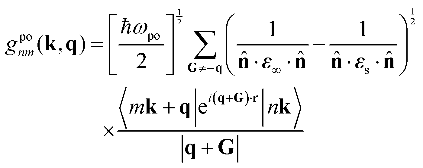 | (7) |
![[n with combining circumflex]](https://www.rsc.org/images/entities/b_char_006e_0302.gif) is a unit vector describing the direction of the phonon wavevector, while ε∞ and εs are the high-frequency and static dielectric tensors of the material, respectively. The expression
is a unit vector describing the direction of the phonon wavevector, while ε∞ and εs are the high-frequency and static dielectric tensors of the material, respectively. The expression  characterizes the difference in dielectric screening between high and low frequencies, influencing the strength of the long-range Coulomb interactions between electrons and phonons in polar materials.
In polar semiconductors, the charge carriers and the surrounding lattice deformation form a so-called polaron,45 which determines the nature of carrier transport. Polarons can be classified into small and large ones based on the strength of electron phonon coupling. The lattice deformation in a large polaron is usually moderate and spreads over multiple unit cells, resulting in a larger mobility. The electron–phonon interaction is usually dominated by the coupling of charge carriers to the longitudinal optical phonons, which can be described within the Fröhlich model.46 The coupling strength between electrons and polar optical phonons is quantified using the Fröhlich coupling constants32,47
 | (8) |
 is the CBM electron effective mass, and ε0 is the vacuum permittivity. The above relevant material parameters of Ga2O3 are listed in Tables 2 and 5. The calculated α (shown in Table 4) shows the averaged value of 1.16, 1.25 and 1.17 for Ga2O3, Al–Ga2O3 and In–Ga2O3, which falls in the intermediate electron–phonon coupling regime (defined as 0.5 ≤ α ≤ 6). The magnitudes of α for Ga2O3 and In–Ga2O3 are quite close, suggesting similar electron–phonon interaction strengths. We further estimate the size of polarons in Ga2O3, Al–Ga2O3 and In–Ga2O3, by the Schultz polaron radius (rf).47 The large values of electron polaron radius (which extend over multiple structural units) indicate that the polarons are delocalized in these Ga2O3. Al–Ga2O3 has the smallest Schultz Polaron radius while Ga2O3 has the largest one, suggesting that the Fröhlich coupling strength of In–Ga2O3 is slightly larger than Ga2O3, and smaller than that of Al–Ga2O3.
| α | r f (Å) | |||||
|---|---|---|---|---|---|---|
| Ga2O3 | Al–Ga2O3 | In–Ga2O3 | Ga2O3 | Al–Ga2O3 | In–Ga2O3 | |
| Average | 1.16 | 1.25 | 1.17 | 145.8 | 138.1 | 142.3 |
g
po
nm
(k, q) is proportional to the frequency of the polar optical phonon mode, ωpo, and inversely proportional to the electronic high-frequency dielectric constant, ε∞. As ε∞ is much smaller than εs, the value of  is almost equal to
  .
.
For purposes of the screening, we assume that the high-frequency dielectric constant is isotropic. Indeed, our DFPT calculations (see Table 5) show that the high-frequency part of the dielectric tensor is nearly isotropic, with values ranging between 3.98 and 4.10 depending on the direction, close to the theoretical value.11,12 In contrast, the static dielectric tensor (εs) shows a stronger directional dependence, which is attributed to the anisotropic ionic contributions to the dielectric tensor in the monoclinic lattice. An averaged value of the computed ε∞ (4.05) is used for calculating gponm(k, q) of Ga2O3. This value is close to the experimental value of ε∞ = 3.60.48 Besides, it is obvious that the ε∞ of In–Ga2O3 is the largest, and the ωpo of In–Ga2O3 is the smallest, indicating gponm of In–Ga2O3 might be the smallest among these three structures according to formula (7).
| Materials | ε ∞ | ε s | ω po (THz) | ||||||
|---|---|---|---|---|---|---|---|---|---|
| a | b | c | Average | a | b | c | Average | ||
| Ga2O311 | 4.07 | 4.14 | 4.19 | 4.13 | 10.99 | 10.50 | 13.91 | 11.80 | 12.08, 8.46–11.6049 |
| Ga2O312 | 4.02 | 4.03 | 4.15 | 4.10 | 11.88 | 9.22 | 12.61 | 11.24 | |
| Ga2O3 | 3.98 | 4.06 | 4.10 | 4.05 | 10.20 | 9.55 | 13.71 | 11.15 | 13.12 |
| Al–Ga2O3 | 3.91 | 3.99 | 4.00 | 3.97 | 10.09 | 9.48 | 13.04 | 10.87 | 12.75 |
| In–Ga2O3 | 4.01 | 4.10 | 4.12 | 4.08 | 10.32 | 9.49 | 13.90 | 11.24 | 12.71 |
We further analyze the individual contribution of POP scattering, as shown in Fig. 5. The mobility of Ga2O3, Al–Ga2O3, and In–Ga2O3 exhibits similar variation curves with temperature, in which the mobility of In–Ga2O3 by POP individual scattering is always the highest. μPOP reduces monotonically as the temperature increases. Since as temperature further increases, more polar optical phonons are excited which can induce a macroscopic electric field, thus strengthening the electron–phonon coupling.
 | ||
| Fig. 5 Temperature-dependent electron mobility of Ga2O3, Al-doped Ga2O3 and In-doped Ga2O3, where only POP scattering is considered. | ||
3.4. Electrical transport properties caused by IMP
The ionized impurity matrix element is given by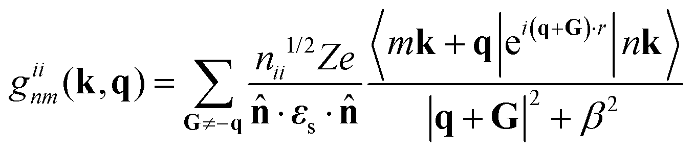 | (9) |
·εs· modulates the strength of the Coulomb interaction due to screening effects. The denominator |q + G|2 + β2 accounts for the momentum transfer q + G during scattering, with β representing a screening length parameter that modulates the range of the interaction.
As shown in Fig. 6a, the mobility due to IMP slightly increases with rising temperature because, as the temperature increases, the kinetic energy of electrons increases, causing them to move faster and spend less time near recombination centers, thereby reducing the probability of scattering. Besides, our research has shown that the mobility of In–Ga2O3 is always higher than that of pure Ga2O3 and Al–Ga2O3. This might be partly attributed to the larger εs of In–Ga2O3.
 | ||
| Fig. 6 Temperature-dependent electron mobility of Ga2O3 at electron concentrations (1 × 1017 cm−3) where only IMP scattering is considered (a). Temperature-dependent electron mobility of Ga2O3 at various electron concentrations where ADP, IMP and POP scattering are considered together (b). | ||
The electron concentration is varied from 1013 cm−3 to 1018 cm−3 to explore the concentration dependent electron mobility of Ga2O3, Al–Ga2O3 and In–Ga2O3, respectively, as shown in Fig. 6b. With electron concentration increasing from 1013 to 1016 cm−3, the electron mobility of In–Ga2O3 slightly drops from 228.9 cm2 V−1 s−1 to 211.7 cm2 V−1 s−1 at 300 K, respectively, which indicates the electron mobility of In–Ga2O3 remains essentially stable. After that, a further increase in electron concentration (from 1016 to 1018 cm−3) rapidly deteriorates electron mobility, from 211.7 cm2 V−1 s−1 to 138.4 cm2 V−1 s−1 at 300 K. This is caused by the strong scattering of excessive carrier concentration with electrons and phonons. According to formula (9), the scattering intensity is positively correlated with impurity concentration nii: the higher the impurity (electron) concentration, the greater the electron scattering intensity, which hinders movement and decreases mobility.
Based on Fig. 4b, 5 and 6a, in the temperature range of 105–150 K, μIMP is the lowest, indicating IMP scattering dominates the electron transport. In the temperature range of 150–650 K, μADP and μIMP are much higher than μPOP, indicating that POP scattering dominates the carrier transport of these three Ga2O3. Fig. 7 shows the effect of temperature on overall mobility, considering ADP, IMP, and POP together. Following Matthiessen's rule,50 the total mobility μtotal is determined from μtotal−1 = μADP−1 + μIMP−1 + μPOP−1. The total mobility is primarily determined by the smallest partial mobility. Overall, ADP has little effect on the total electron mobility. At low temperatures, impurity scattering significantly impacts the total electron mobility; as the temperature increases, optical phonon scattering gradually becomes the dominant scattering mechanism. The magenta curve in Fig. 7 shows the experimentally measured Hall mobility of pure Ga2O3,9 while the black curve represents the mobility of pure Ga2O3 calculated in this study. The high degree of overlap between these two curves indicates the reliability of the calculation method employed in this research. The overall mobility of In–Ga2O3 (blue curve) is the highest from 105 to 650 K, and the electron mobilities of Ga2O3, Al–Ga2O3 and In–Ga2O3 are 151.5 cm2 V−1 s−1, 137.8 cm2 V−1 s−1 and 184.9 cm2 V−1 s−1 at 300 K. Since the effective mass of In–Ga2O3 is smaller than that of Ga2O3 and Al–Ga2O3, it still possesses higher mobility despite its slightly larger electron–phonon coupling strength.
 | ||
| Fig. 7 Temperature-dependent electron mobility of Ga2O3, Al-doped Ga2O3 and In-doped Ga2O3, where ADP, IMP and POP scattering are considered together. | ||
4. Conclusions
To summarize, we have investigated the temperature-dependent electron mobility of Ga2O3, Al–Ga2O3 and In–Ga2O3 from first-principles by fully considering the scattering mechanisms of ADP, IMP, and POP. The results show that POP scattering is the dominant factor limiting the electron mobility of Ga2O3, Al–Ga2O3 and In–Ga2O3 between 150 and 650 K. Combining these three scattering mechanisms, the electron mobilities of Ga2O3, Al–Ga2O3 and In–Ga2O3 are 151.5 cm2 V−1 s−1, 137.8 cm2 V−1 s−1 and 184.9 cm2 V−1 s−1 at 300 K. Furthermore, as temperature increases, the electron mobility of three Ga2O3 reduces due to more excited optical phonons, thus enhancing the electron–phonon coupling. With electron concentration increasing, the electron mobility of three Ga2O3 reduces due to more scattering probabilities. The electron mobility of In–Ga2O3 is the highest among these three structures for the decreased effective mass caused by the In 5s state. This work offers an alternative method to boost the electron mobility of Ga2O3 and serves as a guide for engineering the electronic transport properties tailored for high-power electronic applications.Author contributions
L. Z.: conceptualization, software, writing – original draft. J. H.: validation. Y. S.: writing – review & editing. F. L. and P. Z: formal analysis, visualization. D. W.: visualization. K. W.: writing – review & editing, supervision. Y. W.: writing – original draft, supervision.Data availability
The data that support the findings of this study are available within the article and the ESI.†Conflicts of interest
There are no conflicts to declare.Acknowledgements
This work is financially supported by the National Natural Science Foundation of China (Grant No. 61904071), the QingLan Project of Jiangsu Provincial University of China and the Science Foundation of Jinling Institute of Technology (jit-rcyj-202001). We are thankful for the technology support from the National Supercomputer Center (TianHe-2) in Lvliang.References
- X. He, J. Hu and Z. Zhang, et al., Study on the interface electronic properties of AlN(0001)/β-Ga2O3 (100), Surf. Interfaces, 2022, 28, 101585 CrossRef CAS.
- N. Pant, W. Lee and N. Sanders, et al., Increasing the mobility and power-electronics figure of merit of AlGaN with atomically thin AlN/GaN digital-alloy superlattices, Appl. Phys. Lett., 2022, 121(3), 032105 CrossRef CAS.
- C. J. H. Wort and R. S. Balmer, Diamond as an electronic material, Mater. Today, 2008, 11, 22–28 CrossRef CAS.
- H. H. Tippins, Optical absorption and photoconductivity in the band edge of β-Ga2O3, Phys. Rev., 1965, 140(1A), A316–A319 CrossRef.
- K. Wu, L. Zhang, F. Li, L. Sang, M. Liao, K. Tang, J. Ye and S. Gu, Enhancement of interfacial thermal conductance by introducing carbon vacancy at the Cu/diamond interface, Carbon, 2024, 223, 119021 CrossRef CAS.
- M. Higashiwaki, K. Sasaki and A. Kuramata, et al., Gallium oxide Ga2O3 metal-semiconductor field-effect transistors on single-crystal β-Ga2O3 substrates, J. Appl. Phys. Lett., 2012, 100(1), 013504 CrossRef.
- Z. Galazka, R. Uecker and K. Lrmscher, et al., Czochralski growth and characterization of β-Ga2O3 single crystalsJ, Cryst. Res. Technol., 2010, 45(12), 1229–1236 CrossRef CAS.
- Encarnación G. Villora, Kiyoshi Shimamura, Takekazu Ujiie and Kazuo Aoki, Electrical conductivity and lattice expansion of β-Ga2O3 below room temperature, Appl. Phys. Lett., 2008, 92, 202118 CrossRef.
- N. Ma, N. Tanen, A. Verma, Z. Guo, T. Luo, H. (Grace) Xing and D. Jena, Intrinsic Electron Mobility Limits in -Ga2O3, Appl. Phys. Lett., 2016, 109, 212101 CrossRef.
- Z. Zhang, Y. Wu, C. Lu and S. Ahmed, Electron mobility in β-Ga2O3: an ensemble Monte Carlo study, Appl. Phys. A, 2018, 124, 637 CrossRef.
- X. Duan, T. Wang, Z. Fu, L. Liu and J. Yang, Nontrivial role of polar optical phonons in limiting electron mobility of two-dimensional Ga2O3 from first-principles, Phys. Chem. Chem. Phys., 2023, 25, 10175–10183 RSC.
- Y. Kang, K. Krishnaswamy, H. Peelaers and C. G. Van de Walle, Fundamental limits on the electron mobility of β-Ga2O3, J. Phys.: Condens. Matter, 2017, 29, 234001 CrossRef PubMed.
- F. Roccaforte, P. Fiorenza, G. Greco, R. L. Nigro, F. Giannazzo, F. lucolano and M. Saggio, Emerging trends in wide band gap semiconductors (SiC and GaN) technology for power devices, Microelectro. Eng., 2018, 187–188, 66–77 CrossRef CAS.
- B. K. Ridley, B. E. Foutz and L. F. Eastman, Mobility of electrons in bulk GaN and AlxGa1-xN/GaN heterostructures, Phys. Rev. B: Condens. Matter Mater. Phys., 2000, 61, 16862–16869 CrossRef CAS.
- C. Zhang, F. Liao, X. Liang, H. Gong, Q. Liu, L. Li, X. Qin, X. Huang and C. Huang, Electronic transport properties in metal doped beta-Ga2O3: A first principles study, Phys. B, 2019, 562, 124–130 CrossRef CAS.
- M. Yu, B. Peng, K. Sun, J. Yu, L. Yuan, J. Hu, Y. Zhang and R. Jia, First principles investigation of photoelectric properties of Ga2O3 Doped with group IV elements (Si,Ge,Sn), Mater. Today Commun., 2023, 34, 105127 CrossRef CAS.
- P. Li, L. Dong, C. Li, B. Lu, C. Yang, B. Peng, W. Wang, Y. Miao and W. Liu, Indium doping-assisted monolayer Ga2O3 exfoliation for performance-enhanced MOSFETs, Nanoscale, 2023, 15, 12105–12115 RSC.
- W. Tian, C. Zhi, T. Zhai, S. Chen, X. Wang, M. Liao, D. Golberg and Y. Bando, In-doped Ga2O3 nanobelt based photodetector with high sensitivity and wide-range photoresponse, J. Mater. Chem., 2012, 22, 17984–17991 RSC.
- L. Ji, X. Chen, X. Su, J. Wan, Z. Tu, H. Wu and C. Liu, Influence of indium doping on electrical performance of gallium oxide thin-film transistors, Appl. Phys. Lett., 2023, 122, 202105 CrossRef CAS.
- J. Rehm, T. Chou, S. B. Anooz, P. Seyidov, A. Fiedler, Z. Galazka and A. Popp, Perspectives on MOVPE-grown (100) β-Ga2O3 thin films and its Al-alloy for power electronics application, Appl. Phys. Lett., 2022, 121, 240503 CrossRef CAS.
- Z. Xi, N. Chen, J. Cai, C. Xu, S. Li and S. Zheng, Modulation of electronic structures and transport properties in 2D TM0.5Ga1.5O3 (TM = Al, Ga, In), Phys. Lett. A, 2024, 525, 129914 CrossRef CAS.
- G. Kresse and J. Furthmüller, Efficient iterative schemes for ab initio total energy calculations using a plane-wave basis set, Phys. Rev. B: Condens. Matter Mater. Phys., 1996, 54, 11169 CrossRef CAS PubMed.
- G. Kresse and J. Furthmüller, Efficiency of ab-initio total energy calculations for metals and semiconductors using a plane-wave basis set, Comput. Mater. Sci., 1996, 6, 15 CrossRef CAS.
- J. P. Perdew, K. Burke and M. Ernzerhof, Generalized gradient approximation made simple, Phys. Rev. Lett., 1996, 77, 3865 CrossRef CAS PubMed.
- J. Heyd, G. E. Scuseria& and M. Ernzerhof, Hybrid functionals based on a screened Coulomb potential, J. Chem. Phys., 2003, 118, 8207 CrossRef CAS.
- S. Poncé, W. Li, S. Reichardt and F. Giustino, First-principles calculations of charge carrier mobility and conductivity in bulk semiconductors and two-dimensional materials, Rep. Prog. Phys., 2020, 83, 036501 CrossRef PubMed.
- S. Poncé, E. R. Margine and F. Giustino, Towards predictive many-body calculations of phonon-limited carrier mobilities in semiconductors, Phys. Rev. B, 2018, 97, 121201 CrossRef.
- W. Li, Electrical transport limited by electron-phonon coupling from Boltzmann transport equation: An ab initio study of Si, Al, and MoS2, Phys. Rev. B: Condens. Matter Mater. Phys., 2015, 92, 075405 CrossRef.
- A. M. Ganose, J. Park, A. Faghaninia, R. Woods-Robinson, K. A. Persson and A. Jain, Efficient calculation of carrier scattering rates from first principles, Nat. Commun., 2021, 12, 2222 CrossRef CAS PubMed.
- G. Grimvall, The Electron-Phonon interaction in metals, North-Holland, Amsterdam, 1981 Search PubMed.
- F. Giustino, M. L. Cohen and S. G. Louie, Electron-phonon interaction using Wannier functions, Phys. Rev. B: Condens. Matter Mater. Phys., 2007, 76, 165108 CrossRef.
- H. Fröhlich, Electrons in lattice fields, Adv. Phys., 1954, 3, 325–361 CrossRef.
- H. Brooks, Scattering by ionized impurities in semiconductors, Phys. Rev., 1951, 83, 879 CAS.
- C. Herring and E. Vogt, Transport and deformation-potential theory for many-valley semiconductors with anisotropic scattering, Phys. Rev., 1956, 101, 944 CrossRef CAS.
- J. Bardeen and W. Shockley, Deformation potentials and mobilities in non-polar crystals, Phys. Rev., 1950, 80, 72 CrossRef CAS.
- F. S. Khan and P. B. Allen, Deformation potentials and electron-phonon scattering: Two new theorems, Phys. Rev. B: Condens. Matter Mater. Phys., 1984, 29, 3341 CrossRef.
- E. Kartheuser and S. Rodriguez, Deformation potentials and the electron-phonon interaction in metals, Phys. Rev. B: Condens. Matter Mater. Phys., 1986, 33, 772 CrossRef CAS PubMed.
- R. Resta, Deformation-potential theorem in metals and in dielectrics, Phys. Rev. B: Condens. Matter Mater. Phys., 1991, 44, 11035 CrossRef PubMed.
- S. Geller, Crystal Structure of β-Ga2O3, J. Chem. Phys., 1960, 33, 676–684 CrossRef CAS.
- Q. Fan, R. Zhao, W. Zhang, Y. Song, M. Sun and U. Schwingenschlögl, Low-energy Ga2O3 polymorphs with low electron effective masses, Phys. Chem. Chem. Phys., 2022, 24, 7045–7049 RSC.
- S. J. Pearton, J. Yang, P. H. Cary, F. Ren, J. Kim, M. J. Tadjer and M. A. Mastro, A review of Ga2O3 materials, processing, and devices, Appl. Phys. Lett., 2018, 5, 011301 Search PubMed.
- Effective Mass Calculator for Semiconductors, Fonari A, Sutton C, https://github.com/afonari/emc2013-3-18.
- K. Adachi, H. Ogi, N. Takeuchi, N. Nakamura, H. Watanabe, T. Ito and Y. Ozaki, Unusual elasticity of monoclinic β-Ga2O3, J. Appl. Phys., 2018, 124, 085102 CrossRef.
- M. H. Wong, K. Sasak, A. Kuramata, S. Yamakoshi and M. Higashiwaki, Electron channel mobility in silicon-doped Ga2O3 MOSFETs with a resistive buffer layer, Jpn. J. Appl. Phys., 2016, 55, 1202B9 CrossRef.
- D. Emin, Polarons, Cambridge University Press, 2013 Search PubMed.
- H. Fröhlich, Interaction of electrons with lattice vibrations, Proc. Math. Phys. Eng., 1952, 215, 291–298 Search PubMed.
- J. M. Frost, Calculating polaron mobility in halide perovskites, Phys. Rev. B, 2017, 96, 195202 CrossRef.
- G. Schmitz, P. Gassmann and R. Franchy, A combined scanning tunneling microscopy and electron energy loss spectroscopy study on the formation of thin, well-ordered β-Ga2O3 films on CoGa (001), J. Appl. Phys., 1998, 83, 2533–2538 CrossRef CAS.
- T. Onuma, S. Saito, K. Sasaki, K. Goto, T. Masui, T. Yamaguchi, T. Honda, A. Kuramata and M. Higashiwaki, Temperature-dependent exciton resonance energies and their correlation with IR-active optical phonon modes in β-Ga2O3 single crystals, App. Phys. Lett., 2016, 108, 101904 CrossRef.
- B. R. Nag, Electron Transport in Compound Semiconductors, Springer Berlin Heidelberg, Berlin, Heidelberg, 1980, vol. 11 Search PubMed.
Footnote |
| † Electronic supplementary information (ESI) available. See DOI: https://doi.org/10.1039/d4cp04220d |
| This journal is © the Owner Societies 2025 |