
 Open Access Article
 This Open Access Article is licensed under a
 Creative Commons Attribution 3.0 Unported Licence
Structure and thermal boundary resistance of basal plane twin boundaries in Bi2Te3†
Aoife K.
Lucid
*a,
Javier F.
Troncoso
b,
Jorge
Kohanoff
 c,
Stephen
Fahy
de and
Ivana
Savić
*f
c,
Stephen
Fahy
de and
Ivana
Savić
*f
aTyndall National Institute, Lee Maltings, Dyke Parade, Cork T12 R5CP, Ireland. E-mail: aoife.lucid@tyndall.ie
bAIMEN Technology Centre, Smart Systems and Smart Manufacturing, Artificial Intelligence and Data Analytics Laboratory, PI. Cataboi, 36418 Porriño, Spain
cInstituto de Fusión Nuclear “Guillermo Velarde”, Universidad Politécnica de Madrid, 28006 Madrid, Spain
dTyndall National Institute, Lee Maltings, Dyke Parade, Cork T12 R5CP, Ireland
eDepartment of Physics, University College Cork, College Road, Cork T12 K8AF, Ireland
fDepartment of Physics, King's College London, The Strand, WC2R 2LS London, UK. E-mail: ivana.savic@kcl.ac.uk
First published on 10th April 2025
Abstract
The nanostructuring of thermoelectric materials is a well-established method of suppressing lattice thermal conductivity. However, our understanding of the interfaces that form as a result of nanostructure engineering is still limited. In this work, we utilise a simple two-body pair potential to calculate the thermal boundary resistance of basal plane twin boundaries in Bi2Te3 at 300 K using reverse non-equilibrium molecular dynamics simulations. The considered interatomic potential gives an excellent description of the twin boundary formation energies and the lattice thermal conductivity of bulk Bi2Te3. Using this potential, we find that the twin boundary located at the Bi layer is not thermally stable (unlike those located at the Te layers), and undergoes a phase transition into two distinct structures. We compare the thermal boundary resistance across these different twin boundaries and link the observed trends to overall geometry, van der Waals gap sizes and degree of structural disorder in atomic layers near the boundary.
1 Introduction
Increasing the efficiency of thermoelectric (TE) materials beyond the current state-of-the-art would allow for efficient conversion of waste heat and solar thermal energy into electricity, reducing the demand for fossil fuels and contributing to global decarbonistion.1 Increased efficiency, particularly near room temperature, could provide power sources for a range of emerging technologies, e.g. wireless sensor networks for the Internet of Things, environmental sensing, and point of care medical diagnostics.2–4 The efficiency of TE materials is linked to the dimensionless figure of merit (ZT) of a material, given by5 | (1) |
Nanostructuring has transformed the field of thermoelectrics.13–16 The concept of controlling materials at the nanoscale allows for the engineering of new routes to optimised TEs, including reducing κL. Advancing beyond the current state-of-the-art TEs requires a detailed understanding of the impact of interfaces on transport properties.17 Nanostructured materials are generally highly polycrystalline, see Fig. 1. Ideally, interfaces (such as grain boundaries) could be specifically engineered to optimise transport properties in TE materials, by biasing grain boundaries (GBs) towards structures which offer reduced κL due to phonon scattering at the boundary but are minimally harmful to electronic transport. Growth and identification of these specific interfaces experimentally is a challenging, expensive, and time-consuming process, making computational studies at an atomistic level crucial to unlocking the potential of interface engineering in TE materials.18
 | ||
| Fig. 1 Schematic of a nanostructured bulk (polycrystalline) system highlighting a grain boundary structure at the interface of two grains, in this case a 60° twin boundary. Bi atoms are shown in purple and Te atoms are shown in gold. | ||
In recent years, grain boundaries in Bi2Te3-based materials have become a subject of intense investigation.19–23 Ji et al.23 and He et al.24 carried out experimental proof-of-principle studies on GB engineering of p-type Bi2Te3 which provided new possible routes to the decoupling of the constituent factors of ZT. More recently, Li et al.25 carried out precision GB engineering in Bi2Te2.7Se0.3 (BTS), in which they observed both a reduced κL and enhanced power factor (σ2S) leading to a net enhancement of ZT. Li et al.26 used atomic layer deposition to control and modify grain boundaries of BTS with thin layers of ZnO, resulting in enhancement in ZT of ≈1.8 times when compared to pure BTS. Li et al.27 also undertook a study of atomic-scale tuning of oxygen-doped BTS. Through atomic-scale engineering of interfaces (dislocations), they found that the link between S and σ was broken, resulting in an enhanced S and σ in tandem with a suppressed κL. Studies of interface engineering in TEs have not only been limited to Bi2Te3-based systems. For example, skutterudite based nano-composites28 and IV–VI materials14,29,30 have also been investigated.
There have been a small number of theoretical studies focusing on GBs in Bi2Te3. Medlin et al.31 studied the structure of basal plane twin boundaries (TBs) using density functional theory (DFT) and transmission electron microscopy (TEM) Kim et al.32 investigated free-electron creation at the 60° TB in Bi2Te3, both experimentally and computationally. The shear strength of a selection of TBs in Bi2Te3 was studied by Li et al.33 using DFT. The impact of basal plane TBs on thermal transport in Bi2Te3 was studied by Hsieh and Huang,34 using a well-known three-body interatomic potential (IP)35 with non-equilibrium molecular dynamics (NEMD) methods. They found the least stable TB to have the largest thermal boundary resistance (TBR).
In this work, we focus on the impact of basal plane TBs on thermal transport in Bi2Te3. Basal plane TBs can be located at the Te1, Bi, or Te2 layers, see Fig. 3. TBs, in general, are of interest for a number of reasons. They often occur in materials which have layered structures, such as Bi2Te3, and have been found to be effective in reducing lattice thermal conductivity through phonon scattering and suppression.36–39 Additionally, due to their highly ordered crystal structure, it is expected that TBs would not significantly degrade electronic transport properties.36–39 In Bi2Te3 and its alloys, nanotwinned structures have been found to improve the mechanical strength of the material, which is critical for thermoelectric applications.33,40,41 Twin boundaries formed in alloys of Bi2Te3 with Sb2Te3 have been observed to improve thermoelectric performance.39–41 For these reasons, it is possible that TBs may provide a promising route to the engineering of both thermal and electrical properties in Bi2Te3.
Here, we utilise an IP recently developed for Bi2Te3 by Huang et al.42 (hereafter we use the acronym HLYZ for this IP). We compare this IP to two well-established IPs for bulk Bi2Te3,35,43 as well as to DFT simulations. We find that the HLYZ IP gives an excellent description of bulk Bi2Te3, both at 0 K and at finite temperatures. Basal plane TBs are also well described by this IP at 0 K. Using the HLYZ IP we show that the lower energy TBs (Te1 and Te2) are thermally stable at 300 K, while the Bi TB undergoes a complex phase transition into two structures with different degrees of disorder and sizes of vdW gap. Finally, we investigate the thermal boundary resistance of the Te1, Te2 and Bi TBs at 300 K using reverse NEMD. We find the Te1 TB to be the least resistive to thermal transport across the interface, and observe that for the Te1 and Te2 TBs the calculated thermal boundary resistance follows the same trend as the TB formation energy. The Bi TB structures display the largest TBRs. We explain these findings by analyzing the TB geometry, the size of the vdW gaps and the degree of structural disorder in quintuple layers near the TBs.
2 Methods
2.1 Bi2Te3 and twin boundary structures
The primitive rhombohedral unit cell of Bi2Te3 has space group R![[3 with combining macron]](https://www.rsc.org/images/entities/char_0033_0304.gif) m and contains 5 atoms, while the conventional hexagonal unit cell consists of 15 atoms, or three QLs (Fig. 2). The experimental lattice constant for the rhombohedral cell is arhomb = 10.476 Å; for the hexagonal cell these are ahex = 4.386 Å, and chex = 30.497 Å.44 The primitive cell was used for bulk DFT simulations, while the hexagonal unit cell was used to create TB structures for DFT simulations of TBs. In the case of MD simulations (both bulk and interfaces), orthogonal cells were generated from the hexagonal unit cell.
m and contains 5 atoms, while the conventional hexagonal unit cell consists of 15 atoms, or three QLs (Fig. 2). The experimental lattice constant for the rhombohedral cell is arhomb = 10.476 Å; for the hexagonal cell these are ahex = 4.386 Å, and chex = 30.497 Å.44 The primitive cell was used for bulk DFT simulations, while the hexagonal unit cell was used to create TB structures for DFT simulations of TBs. In the case of MD simulations (both bulk and interfaces), orthogonal cells were generated from the hexagonal unit cell.
 | ||
| Fig. 2 (a) The structure of the primitive rhombohedral unit cell of Bi2Te3, and (b) the structure of the conventional hexagonal unit cell of Bi2Te3 with the quintuple layer structure highlighted. Bi atoms are shown in purple and Te atoms in gold. | ||
The basal plane TBs are shown in Fig. 3, with the interfaces indicated by red dashed lines. The QL structure of Bi2Te3 allows for three locations at which these interfaces can form: the Te1 layer, the Bi layer, or the Te2 layer. These TBs represent a 180° rotation about the [0001] axis, effectively reversing the stacking of the basal plane. To maintain periodic boundary conditions in the c-direction (perpendicular to the basal plane), each TB simulation cell contains two structurally identical but oppositely oriented boundary structures. Interfacial structures were constructed using Atomsk.45 The Open Visualization Tool (OVITO)46 and Visualization for Electronic and STructural Analysis (VESTA)47 were used for visualisation.
 | ||
| Fig. 3 The structure of the basal twin boundaries in Bi2Te3. Bi atoms are shown in purple while Te atoms are shown in gold. The locations of the twin boundaries are indicated by the dashed lines. | ||
2.2 DFT simulation details
DFT simulations were performed using the Vienna ab initio simulation package (VASP).48–51 A plane wave basis set (500 eV cut off) was used with the projector augmented wave (PAW) method52 (Bi[Xe,4f14], Te[Kr,4d10]). The local density approximation (LDA), Perdew–Burke–Ernzerhof (PBE), and PBE modified for solids (PBEsol)53–56 exchange–correlation functionals were considered to determine which is the most suitable for studies of both bulk and interfaces of Bi2Te3. An 8 × 8 × 8 Monkhorst–Pack k-point mesh57 was employed for optimisation of bulk structures. These were considered converged when the forces on all atoms were less than 0.005 eV Å−1. For TB structures, a 30-atom expansion of the conventional hexagonal unit cell was determined to be converged when the forces on all atoms were less than 0.01 eV Å−1. A 7 × 7 × 1 k-point mesh was used for sampling. For both bulk and TBs, the electronic structure was considered converged when the energy difference between self-consistent cycles was less than 10−6 eV. Larger TB simulation cells were tested and no notable change in the energetics was observed.2.3 Twin boundary formation energy
Twin boundary formation energies (ETB) were calculated using | (2) |
2.4 Interatomic potentials
The quality of any classical molecular dynamics (MD) simulations is determined by the IPs employed. In this work, we considered three IPs for thermal transport in Bi2Te3. The Qiu and Ruan (QR) IP43 is a Morse type potential with long-range Coulomb interactions, while the Huang and Kaviany (HK) IP35 is of three-body type, also with Coulomb interactions. Both of these IPs are well known and have been utilised for a variety of MD simulations on Bi2Te3-based material systems.34,58–62 In 2019, a third (HLYZ) IP for Bi2Te3 was developed by Huang et al.42 This IP is of Morse type with no long-range interactions. Therefore, the HLYZ IP is the least computationally expensive of these three IPs, allowing much larger structures to be investigated at longer timescales. Despite its simplicity, the HLYZ IP gives an excellent description of structural, mechanical, and thermal properties of bulk Bi2Te3.42 The majority of the simulations in this work were carried out using the HLYZ IP.2.5 Molecular dynamics methods
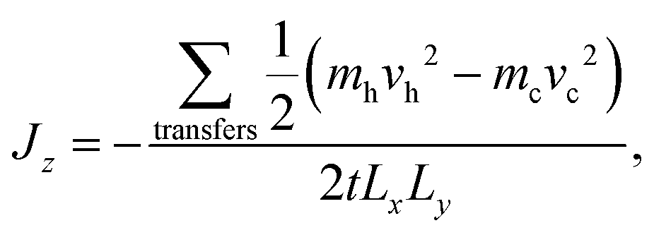
Static (0 K) simulations were carried out using the General Utility Lattice Program (GULP)63 and the Large-scale Atomic/Molecular Massively Parallel Simulator (LAMMPS).64,65 All MD simulations were performed using LAMMPS. Simulations of bulk Bi2Te3 to calculate lattice thermal conductivity were carried out using both equilibrium MD (EMD) with the Green–Kubo method66–68 and reverse non-equilibrium MD (rNEMD).69 Simulations of the thermal boundary resistance of basal plane TBs in Bi2Te3 were carried out using rNEMD. Related approaches have been used for investigations of PbTe,70 silicon-based materials,68,71,72 and carbon-based materials.73,74The implementation of rNEMD in LAMMPS follows the Müller–Plathe method.69 In this method, a heat-flux is imposed on the system and a resultant temperature gradient is calculated. The primary advantage of this method is that the temperature gradient converges faster than the heat-flux, and so by imposing a heat-flux and calculating a temperature gradient simulations should, in principle, be more efficient. The system is split into N equal slabs in the direction perpendicular to heat flow (z-direction), with the middle slab (z = Lz/2) defined as the “hot” slab and the first slab (z = 0) as the “cold” slab, see Fig. 4. The heat-flux is defined by an energy exchange mechanism. Energy is transferred from the hot slab to the cold slab through velocity swapping, where the coldest atom in the hot slab and the hottest atom in the cold slab are exchanged. The energy transferred is known exactly and represents the heat-flux applied to the system (Jz) given as
 | (3) |
 | (4) |
 | ||
| Fig. 4 Top: Schematic of the simulation set-up for reverse non-equilibrium molecular dynamics. Two interfaces shown in yellow are placed in the system halfway between the hot and cold slabs. This set-up utilises periodic boundary conditions. Bottom: A representative temperature profile for a system containing interfaces, showing the temperature discontinuity which appears at the interfaces. | ||
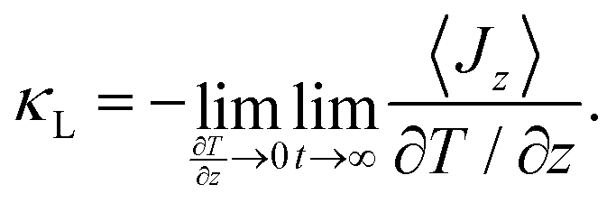
The lattice thermal conductivity of a bulk material is calculated using the temperature gradient ∂T/∂z extracted from a linear fit to the temperature profile.68 To ensure the system is in the linear regime, large temperature differences between the hot and cold slabs should be avoided. This is done by carefully selecting the swap frequency for the aforementioned energy exchange. The more frequent the swaps, the larger the resulting ∂T/∂z, and the more likely it is that the system is no longer in the linear regime. The lattice thermal conductivity of a bulk material is computed using
 | (5) |
In the case of interfacial simulations, a discontinuity will appear in the temperature profile, see Fig. 4. The thermal boundary resistance (TBR) is calculated from the temperature difference at either side of the temperature discontinuity (ΔT) and the heat-flux (Jz) as75
 | (6) |
![[thin space (1/6-em)]](https://www.rsc.org/images/entities/char_2009.gif) 680 atoms) expansions of the orthogonal unit cell of Bi2Te3 were used to compute κL. Systems were first equilibrated for 1 ns in the isothermal–isobaric ensemble (NPT), followed by 1 ns in the isothermal–isochoric ensemble (NVT). Systems were then allowed 250 ps of equilibration in the microcanonical (NVE) ensemble before data collection began. Data collection was carried out for 2.4 ns with a correlation time68,71 of 60 ps. The truncation time68,71 was chosen to be 37.5 ps. Due to the anisotropic nature of Bi2Te3, two κL values were calculated, one for the in-plane direction and one for the cross-plane direction. To account for the statistical nature of MD, results were averaged over 5 independent MD simulations and the standard error was calculated. Periodic boundary conditions were imposed in the x, y, and z directions for all EMD simulations.
680 atoms) expansions of the orthogonal unit cell of Bi2Te3 were used to compute κL. Systems were first equilibrated for 1 ns in the isothermal–isobaric ensemble (NPT), followed by 1 ns in the isothermal–isochoric ensemble (NVT). Systems were then allowed 250 ps of equilibration in the microcanonical (NVE) ensemble before data collection began. Data collection was carried out for 2.4 ns with a correlation time68,71 of 60 ps. The truncation time68,71 was chosen to be 37.5 ps. Due to the anisotropic nature of Bi2Te3, two κL values were calculated, one for the in-plane direction and one for the cross-plane direction. To account for the statistical nature of MD, results were averaged over 5 independent MD simulations and the standard error was calculated. Periodic boundary conditions were imposed in the x, y, and z directions for all EMD simulations.
Fig. 4 shows the rNEMD TB simulation set-up. Each cell contains two identically structured but oppositely orientated TBs located one quarter and three quarters of the way along the length of the simulation cell. The TBR was calculated for a given length Lz, using eqn (6). As the basal plane TBs are located along the cross-plane direction, only heat flow in this direction was considered. These simulations were identical to those for bulk systems in terms of temperature, timestep, equilibration, and data collection for analysis. Finite-length effects are often overlooked in rNEMD simulations of interfaces. To account for these effects, we carried out a number of simulations at different Lz for the Te2 TB, see Table S3 in ESI† for details. The TBR was plotted as a function of Lz to determine the length at which it had converged. The Te1 and Bi TBs were then investigated at the determined converged Lz. Periodic boundary conditions were imposed in the x, y, and z directions for all rNEMD simulations.
3 Results and discussion
3.1 Structural parameters of bulk Bi2Te3
In order to determine which exchange–correlation functional would be most appropriate for our investigations of Bi2Te3, we performed a study of three well-known functionals: LDA, PBE and PBEsol.53–56 Spin–orbit coupling was not included in our ionic relaxations. The structural parameters of bulk Bi2Te3 are presented in Table 1. It is clear that PBEsol shows the best level of agreement when compared with the experimental structure, as all parameters are within 1% of the observed experimental values44 (measured at 300 K). This level of agreement is seen across all structural parameters, including bond lengths, and the interlayer distance between Te1 atoms in adjacent van der Waals layers (deqm, the vdW gap). Other studies have also shown excellent agreement between PBEsol and experiment for the structural description of Bi2Te3.78 Our parameters for the LDA and PBE functionals are also consistent with values calculated in other DFT studies.78 PBEsol will be used for DFT simulations of Bi2Te3 in this work.| Lattice parameter (Å) | Angle (°) | Volume (Å3) | d eqm (Å) | |
|---|---|---|---|---|
| Experiment | 10.4844 | 26.1744 | 169.3644 | 2.6144 |
| LDA | 10.26(−2.04) | 24.50(1.38) | 163.45(−3.49) | 2.51(−3.96) |
| PBE | 10.91(4.13) | 23.55(−2.57) | 181.92(7.42) | 3.05(16.81) |
| PBEsol | 10.40(−0.77) | 24.36(0.78) | 167.95(−0.83) | 2.60(−0.56) |
| HLYZ IP42 | 10.42(−0.52) | 24.20(0.16) | 167.22(−1.26) | 2.55(−2.41) |
| QR IP43 | 10.43(−0.46) | 23.85(−1.32) | 162.86(−3.84) | 2.55(−2.25) |
| HK IP35 | 10.44(−0.37) | 24.08(−0.37) | 166.31(−1.80) | 2.55(−2.23) |
In addition to the values calculated by DFT, the lattice parameters calculated using the three IPs previously discussed are also presented in Table 1. These values are obtained from static simulations at 0 K. While the deqm is not as well described as by PBEsol, all other parameters are generally in good agreement with experiment. The QR IP shows a slightly larger level of disagreement when compared with the other two IPs. The volume, for example, is underestimated by 3.84%. With the exception of the deqm value, both the HLYZ and HK IPs show a similar level of agreement with experiment as the PBEsol simulations.
3.2 Interatomic potentials and bulk thermal conductivity
As discussed in Section 2, there are three existing classical IPs for Bi2Te3. Of particular interest in the context of thermal properties is an accurate description of the phonon dispersion and phonon density of states (DOS). Both the QR and HK IPs fail to properly describe the high frequency optical phonon modes in Bi2Te3, resulting in gaps of 0.4 THz43 and 0.7 THz35 for frequencies roughly between 2 and 3 THz, respectively. This gap is closed by the HLYZ IP,42 providing much better overall agreement with the experimental phonon dispersion and DOS.79 While acoustic phonons dominate heat transport in pure bulk Bi2Te3, Hellman and Broido80 have shown that optical phonon modes provide a large contribution to κL near 300 K. Furthermore, the lifetimes of acoustic phonons depend on their scattering by optical phonons, and may be significantly reduced in the presence of gaps in the phonon density of states.81 This suggests that the improved description of phonon dispersion obtained by the HLYZ IP may result in more accurate κL simulations.We calculate the κL of Bi2Te3 at 300 K using the HLYZ IP. The calculated values using EMD with the Green–Kubo method and rNEMD are presented in Tables 2 and 3, along with values for the QR and HK IPs taken from the literature.35,43,82 The experimental values of the in-plane and cross-plane κL at 300 K are 1.7 W m−1 K−1 and 0.8 W m−1 K−1, respectively.83 The HLYZ IP shows excellent agreement with experiment for both methods of calculation and both directions in Bi2Te3. In the in-plane direction, the EMD value is 1.707 ± 0.017 W m−1 K−1, while the rNEMD value is 1.831 ± 0.004 W m−1 K−1. In the cross-plane direction, the EMD value is 0.718 ± 0.007 W m−1 K−1 and the rNEMD value is 0.751 ± 0.006 W m−1 K−1. The other two IPs give κL values that are in worse agreement with experiment, regardless of the simulation method used, see Tables 2 and 3. A possible explanation for this marked improvement in κL using the HLYZ IP is the aforementioned closing of the gap in the phonon dispersion and DOS.
3.3 Twin boundary formation energy
The formation energies (ETB) of the three basal plane TBs have been calculated using both DFT (PBEsol) and static (0 K) optimisations with the three IPs, see Table 4. According to both our PBEsol calculations and previously published LDA31 calculations, the order of stability is Te1 > Te2 > Bi. While all three IPs agree with DFT in terms of the order of stability, there are some important points to note. In the case of the QR and HK IPs, the Te1 TB is found to be more stable than bulk Bi2Te3 (as indicated by the negative formation energy), which does not agree with the DFT results, and is an unphysical result. Similarly, ref. 34 observed that the Te1 TB was more stable than bulk Bi2Te3 during MD simulations using the HK IP. This was attributed to the Coulomb potential, and it was found that by increasing the cut-off radius of the Coulomb potential by 2 Å, the total potential energy of the Te1 TB was slightly larger than bulk.34 The HLYZ IP predicts the Te1 TB to have a small positive ETB, which is a more physically reasonable result than a negative ETB. Additionally, in the case of the HK IP, the Bi and Te2 TBs are remarkably close in energy when compared to the results from other methods. In the MD simulations of ref. 34, it appears that at 300 K the Bi TB is in fact lower in energy than the Te2 TB when using the HK IP. This is in disagreement with DFT and 0 K IP results reported here. Consequently, the HLYZ IP describes the basal plane TB formation energy in Bi2Te3 more accurately compared to the other two IPs.3.4 Thermal stability of twin boundaries
To investigate thermal transport at interfaces using rNEMD, the interfacial structures should be stable and well-described by the chosen interatomic potential. Previous thermal transport simulations utilising the HK IP suggest that all three TBs are thermally stable within that IP.34 However, the order of stability at 300 K was found to be Te1 > Bi > Te2,34 likely as a result of the energetic similarity between the Bi and Te2 TBs, which we pointed out above.In this work, we utilised MD simulations to test the stability of TBs with the HLYZ and QR IPs. Stability tests were initially carried out in 360 atom orthogonal cells. All systems were equilibrated using both the NPT and NVT ensembles and allowed to run for a minimum of 5 ns in the NPT ensembles. We found that none of the TBs were stable while utilising the QR IP, meaning it is not suitable for studies of thermal transport at these interfaces. The failure of this IP to stabilise was also observed for the Te1 TB by Wang.60
We also found that the Te1 and Te2 twin boundaries are thermally stable using the HLYZ IP. However, we observe an apparent phase transformation in the case of the Bi TB, which was not reported in the study of TBs34 using the HK IP. In 360 atom cells, the resulting structure is similar to the Te1 TB structure. Fig. 5 shows the potential energy per atom of the three TBs over a 5 ns trajectory at 300 K. The Te1 and Te2 TBs remain stable, while the Bi TB undergoes a phase transition, as indicated by the changing potential energy of the system. Note that the final structure of the Bi and Te1 TBs have similar potential energies. Fig. 6 shows the initial structure of the Bi TB, the structure after the first transition point, the structure after the second transition point (i.e. the final structure) and the structure of the Te1 TB. From this, it is clear that the final structure of the Bi TB is very similar to that of the Te1 TB in the simulations with 360 atom cells.
 | ||
| Fig. 5 Potential energy per atom vs. simulation time for basal plane twin boundaries in Bi2Te3 at 300 K for simulation cells with 360 atoms. | ||
 | ||
| Fig. 6 Twin boundary structures taken from the molecular dynamics trajectories in Fig. 5 of (a) the Bi twin boundary, (b) the structure of the Bi twin boundary after the first transition, (c) the structure of the Bi twin boundary after the second transition, and (d) the Te1 twin boundary structure. Bi atoms are shown in purple and Te atoms are shown in gold. | ||
Systematic testing of the phase transition of the Bi TB was carried out on a variety of cell sizes, simulation set-ups and runtimes. Fig. S3 in the ESI† shows a phase transition occurring in Bi twins of various sizes. In all cases, the Bi TB undergoes a structural change. At higher temperatures (500 and 900 K), this change happens more quickly. Despite the instability of the Bi TB, we carried out rNEMD simulations on this system after the phase transition occurs. This was motivated by the excellent description of other properties and other TBs by the HLYZ IP, as well as the correct description of the order of stability at 0 K. To do so, we generated very large (≈ 400000 atoms) simulation cells. In these large systems, structural changes in the Bi TB persist, and fall into two categories with different structures and different TBRs for independent MD runs. This will be discussed in more detail in Section 3.5.
It should be noted that the Bi TB is the least stable TB according to all methods applied in this work, and so it is possible that it is inherently unstable. If there is a true phase transition taking place, it could have significant implications for thermal transport at TBs in Bi2Te3. The only simulation method which can be reliably utilised to test if this is a true phase transition is ab initio MD, which would be very costly and time-consuming in this case. Another option would be the development of a machine learning IP for Bi2Te3 which would be capable of reproducing first-principles levels of accuracy for interfaces.
3.5 Thermal boundary resistance of twin boundaries
 | ||
| Fig. 7 (a) Temperature profiles of the Te2 twin boundary at 300 K with swap frequencies W of 100 and 400, highlighting the impact of parameter choice on temperature difference in the system. The length of this system is Lz ≈ 159 nm. (b) Thermal boundary resistance vs the system length for the Te2 twin boundary at 300 K, with varying swap frequencies, W. | ||
The choice of swap frequency, W, for the energy exchange in rNEMD is also important in determining the temperature gradient, and thus, whether the system is in the linear regime. In Fig. 7(a) and (b) we show the impact of choosing to swap energy too frequently. Fig. 7(b) shows TBR plotted against Lz for W = 100 and 400. It is clear that the W = 100 case has much larger errors associated with it and converges to a different value. This can be attributed to a large temperature difference (225 K) between the hot and cold slab in the simulation. The temperature profile for the case where W = 100 is compared to that where W = 400 is given in Fig. 7(a). In the W = 400 case, the temperature difference between the hot and cold slab is much smaller (65 K). The large temperature difference for W = 100 results in the system being perturbed from the linear regime leading to large errors in the TBR. In systems with inherently low κL, as in the case of Bi2Te3, the importance in the choice of such parameters is magnified. Since the calculated values are so small, even minor errors introduced by errant parameters will contribute significantly to inaccuracies. Careful convergence studies are critical when carrying out such simulations. This has been well illustrated for bulk systems by EI-Genk et al.84
The Bi TB was also simulated at Lz ≈ 159 nm (≈ 400000 atoms). As was briefly mentioned in Section 3.4, the complex instability of the Bi TB leads to two structures and two unique TBR values in these large simulation cells. We labelled these structures as Bi Structure 1 and Bi Structure 2, see Fig. 8(a). Bi Structure 1 appears to be a metastable state of Bi Structure 2. This is illustrated in Fig. S5 of the ESI.† We find in ≈ 50% of our MD simulations that this metastable state remains stable for long enough to carry out rNEMD simulations (up to 40 ns) and calculate a TBR for this structure. The TBR which we observed for Bi Structure 1 was the largest of any we had studied and we decided to investigate it further in an effort to understand its large TBR and how that may be linked to its unusual structure, described in more detail below.
 | ||
| Fig. 8 (a) Structure of the Te1, Te2, Bi Structure 1 and Bi Structure 2 twin boundaries at 300 K for the simulation cell length of Lz ≈ 159 nm. (b) Corresponding thermal boundary resistance (TBR) and van der Waals (vdW) gaps of all four structures. | ||
The Bi Structure 1 interface is characterized by an increased separation of the vdW layers nearest to the TB compared with the other TB structures considered, which can be seen in Fig. 8(a). This results in a very large TBR of (19.470 ± 0.023) × 10−9 m2 K W−1, with ΔT = 9.78 ± 0.13 K. Bi Structure 2 has a highly disordered structure and seemingly the smallest vdW gap, see Fig. 8(a). This structure gives rise to a TBR of (5.331 ± 0.031) × 10−9 m2 K W−1, with ΔT = 2.67 ± 0.16 K. It should be noted that for both Bi Structure 1 and Bi Structure 2, the thermal boundary resistances are calculated only after the phase transition has occurred. Fig. S6, S7 and Tables S5, S6 of the ESI† illustrate this. TBR values of all considered structures (the Te1, Te2, Bi Structure 1 and Bi Structure 2 twin boundaries) are shown in Fig. 8(b).
Since these Bi TB structures were not observed by Hsieh and Huang,34 there are no equivalent values in the literature to compare to. The Bi TB structure in the Hsieh and Huang study had a TBR of (1.26 ± 0.73) × 10−9 m2 K W−1. Fig. S8 in the ESI† compares all values of TBR calculated here with those of Hsieh and Huang.34 All TBR and ΔT values are summarised in Tables S7 and S8 of the ESI.†
First we discuss the differences in the TB geometry shown in Fig. 8(a). For the Te1 TB, the presence of the vdW gap at the interface leads to weak coupling between the quintuple layers adjacent to the TB. As a result, we would expect that interatomic force constants in either of these quintuple layers do not change significantly compared to bulk Bi2Te3. In contrast, the Te2 layer at the Te2 TB is strongly bonded to the adjacent Bi layer, indicating significant changes in the interatomic force constants near the Te2 TB compared to bulk. Similarly, we would expect that the changes in the interatomic force constants near the Bi TB structures with respect to bulk Bi2Te3 are also considerable.
Next, we examine the degree of structural disorder in quintuple layers near the considered TBs, see Fig. 8(a). Bi Structure 2 displays the highest level of disorder. There is also some disorder present in the Te1 layers adjacent to the Bi Structure 1 interface, but much less than in Bi Structure 2. In contrast to the Bi TB structures, the Te1 and Te2 TBs are highly crystalline.
We also compute the size of the vdW gaps (deqm) for all TBs considered, both at the interface and in the bulk part of the simulation cell, see Table 5 and Fig. 8(b). The deqm values from MD simulations are calculated by averaging the distances between the adjacent Te1 layers across multiple snapshots along the MD trajectory. The values of deqm for all TBs in the bulk part of the simulation cell are very similar to that of bulk Bi2Te3 (2.655 ± 0.008 Å). Moreover, the sizes of the vdW gaps near the Te1 and Te2 TBs are also close to the bulk value. However, the deqm in the immediate vicinity of Bi Structure 1 is 3.585 ± 0.109 Å, which is 1 Å larger than that of bulk. The deqm near Bi Structure 2 is 2.491 ± 0.173 Å, which is slightly smaller compared to bulk Bi2Te3 and has a much larger deviation.
| Bulk | Te2 | Te1 | Bi Structure 1 | Bi Structure 2 | |
|---|---|---|---|---|---|
| d eqm bulk (Å) | 2.655 ± 0.008 | 2.649 ± 0.029 | 2.652 ± 0.033 | 2.648 ± 0.047 | 2.659 ± 0.035 |
| d eqm TB (Å) | — | 2.657 ± 0.031 | 2.629 ± 0.045 | 3.585 ± 0.109 | 2.491 ± 0.173 |
We now examine the influence of the TB structure on the TBR (summarized in Fig. 8), starting with the Bi TBs. Bi Structure 1 has the largest TBR by at least a factor of three when compared to the other TBs. Fig. 8 suggests that the large vdW gap, in conjunction with a degree of disorder, effectively inhibits the thermal conduction across this TB. It may seem somewhat surprising that highly disordered Bi Structure 2 has a substantially lower TBR compared to Bi Structure 1. However, Bi Structure 1 has 1 Å larger vdW gap than Bi Structure 2, which appears to be much more effective in blocking heat conduction than a high degree of disorder.
Next, we investigate the impact of structure on the TBR of Bi Structure 2 and the Te2 TB. Even though Bi Structure 2 is highly disordered, and the Te2 TB is highly crystalline, their TBRs are comparable (Fig. 8(b)). This is likely due to the slightly smaller vdW gap of Bi Structure 2, which also exhibits large deviations. While we might expect the disorder to contribute to a larger TBR of Bi Structure 2, the reduction of the vdW gap appears to compensate for this to some degree, resulting in a TBR comparable to that of the Te2 TB. These findings suggest that the vdW gap size in layered materials is another potential knob for controlling the TBR of their interfaces, in addition to the overall geometry and structural disorder within the layers.
Finally, we investigate the differences in the TBR values of the Te1 and Te2 TBs. The Te1 TB has the lowest TBR of all systems considered, roughly a factor of three smaller than the TBR of the Te2 TB. The Te1 and Te2 TBs are both highly crystalline and their vdW gaps are similar in size. However, the changes of the interatomic force constants near the interface compared to bulk are expected to be smaller in the Te1 TB than in the Te2 TB, because the quintuple layers on both sides of the Te1 TB are weakly coupled via the vdW gap. As a result, the Te1 TB has a smaller TBR than the Te2 TB. This weak coupling across the Te1 TB also leads to the lower formation energy of the Te1 TB than that of the Te2 TB, as shown in Table 4.
The influence of the size of the vdW gap on the phonon transmission across the vdW gap in bulk materials has been studied in ref. 89 and 90. The phonon transmission across a vdW gap in bulk Bi2Te3 increases if the strength of the vdW interaction increases,89 and the strength of the vdW interaction increases as the vdW gap size decreases.90 The phonon transmission appropriately integrated over the phonon spectrum gives the thermal boundary conductance,91,92 which is the inverse of the thermal boundary resistance. Therefore, the qualitative picture emerging from ref. 89 and 90 is that the thermal boundary resistance across a vdW interface should increase as the size of the vdW gap increases. This is in qualitative agreement with our calculations and analysis, even though our systems are more complex due to the presence of disorder and different bonding geometry for different structures. Indeed, our structure with the largest vdW gap has the largest thermal boundary resistance (Fig. 8(b)).
As previously stated, the Bi TB is the least stable interface at 0 K across all methods utilised in this study and so it is possible that it is inherently unstable. The results presented here suggest that unravelling the relationship between structure, energetics, and thermal transport in Bi2Te3 interfaces is a complex problem which may necessitate the development of more sophisticated IPs. Nevertheless, our conclusions related to the impact of disorder and the position and size of van der Waals gaps on interfaces in layered materials are expected to be general and not limited to the specific case of Bi2Te3 and the TBs considered here. Our results show that disordered interfaces near, but not immediately at, large vdW gaps should have large thermal boundary resistances and lead to large lattice thermal conductivity reductions in layered materials.
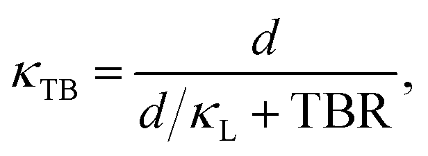 | (7) |
Fig. 9 shows that Bi Structure 1 to have the largest impact on lattice thermal conductivity when compared to bulk, with a reduction of ≈ 15% for the grain size of d = 79.5 nm. This is a significant reduction considering the already low κL of bulk Bi2Te3 (0.751 W m−1 K−1). A reduction of this magnitude is not easily achieved in materials with such low lattice thermal conductivity. In cases where the material is alloyed (as is often true for Bi2Te3), this reduction would be even larger due to the combined effects of alloy and interface scattering. The reductions observed for the other twin boundaries are lower, but not insignificant, see Fig. 9. The Te1 TB shows a reduction of ≈ 1.4%. This low reduction in lattice thermal conductivity is not surprising considering the bulk-like structure of the Te1 TB. This result suggests that the Te1 TB should not be targeted for the reduction of κL. For the Te2 and Bi Structure 2 TBs, reductions of ≈ 4.3% and ≈ 4.8% are observed, respectively. We have tabulated the κTB values as well as their reduction compared to bulk in Table S9 in the ESI.†
 | ||
| Fig. 9 The effective lattice thermal conductivity (κTB) of the superlattice-like systems containing all considered twin boundaries with the grain size of d = 79.5 nm (black dots), alongside the cross-plane lattice thermal conductivity (κL) for bulk Bi2Te3 (red-dashed line). All results are obtained for the temperature of 300 K. | ||
4 Conclusions
We find that the recently developed IP by Huang et al.42 gives an excellent description of bulk Bi2Te3 (both at 0 K and 300 K), as well as basal plane twin boundaries (TBs) at 0 K. Using both DFT methods and the IP of Huang et al.42 we show that the order of stability for the TBs at 0 K is Te1 > Te2 > Bi. We observed thermal stability for the Te1 and Te2 TBs at 300 K, while the Bi TB appears to be unstable, undergoing a complex phase transition. The Bi TB is the least energetically stable of the three TBs, so it is possible that it is inherently unstable. Higher level methods (ab initio MD, machine learned IPs) are required to determine if this is a realistic structural change.The Te1 TB is found to be the least resistive to thermal transport owing to its bulk-like structure, reducing the lattice thermal conductivity of the system by only ≈ 1.4% when the distance between the grain boundaries is ≈ 80 nm. This suggests that the Te1 TB should be avoided when aiming to reduce lattice thermal conductivity. The structure with the highest thermal boundary resistance is a metastable phase transition of the Bi twin boundary (Bi Structure 1), which reduces the lattice thermal conductivity by ≈ 15% when the distance between the grain boundaries is ≈ 80 nm. This is a significant reduction considering the lattice thermal conductivity of bulk Bi2Te3 is found to be only 0.751 W m−1 K−1.
We rationalize the thermal boundary resistance (TBR) values of all TBs considered by examining their overall structure, the degree of structural disorder and the size of the van der Waals gaps in quintuple layers near the boundaries. The Te1 TB has the lowest TBR due to the presence of the vdW gap right at the boundary. The Bi TB structure with the largest TBR (Bi Structure 1) is one in which the van der Waals gap between the Te1 layers near the TB is considerably increased compared to its bulk value and where there is disorder present in the Te1 layers. The TBR of Bi Structure 2, which has the smallest van der Waals gap and the largest degree of disorder near the TB, is significantly lower than that of Bi Structure 1 and comparable to that of the Te2 TB. Our results indicate that varying the position and size of the vdW gap near a grain boundary in layered materials can significantly impact its TBR, in addition to varying structural disorder within the layers. Based on these results, we propose that disordered interfaces near large vdW gaps in layered materials should enable large reductions of their lattice thermal conductivity and potentially improve their thermoelectric properties.
Author contributions
A. K. L. and I. S. conceived the research plan. A. K. L. performed the calculations. A. K. L. and I. S. wrote the manuscript. All authors discussed the results and commented on the manuscript.Data availability
DFT simulations were performed using the Vienna ab initio simulation package (VASP)48–51 (https://www.vasp.at/). Static (0 K) simulations were carried out using the General Utility Lattice Program (GULP)63 (https://gulp.curtin.edu.au/) and the Large-scale Atomic/Molecular Massively Parallel Simulator (LAMMPS)64,65 (https://www.lammps.org/). All molecular dynamics simulations were performed using LAMMPS.Conflicts of interest
There are no conflicts to declare.Acknowledgements
A. K. L. was supported by the Irish Research Council Postdoctoral Fellowship Scheme (GOIPD/2021/823). A. K. L. and I. S. were supported by the Science Foundation Ireland CONNECT Centre (13/RC/2077). A. K. L., I. S., S. B. F., J. F. T., and J. K. were supported by Science Foundation Ireland (SFI) and the Department for the Economy Northern Ireland under the SFI-DfE Investigators Programme Partnership (15/IA/3160). J. K. was supported by the Beatriz Galindo Program (BEAGAL18/00130) from the Ministerio de Educación y Formación Profesional of Spain, and by the Comunidad de Madrid through the Convenio Plurianual with Universidad Politécnica de Madrid in its line of action Apoyo a la realizaci'on de proyectos de I + D para investigadores Beatriz Galindo, within the framework of V PRICIT (V Plan Regional de Investigación Científica e Innovación Tecnológica). Simulations were performed using the rocks supercomputer, maintained by Tyndall National Institute, and the Kay supercomputer, maintained by the Irish Centre for High-End Computing (ICHEC).References
- D. Champier, Energy Convers. Manage., 2017, 140, 167–181 CrossRef.
- Z. Han, J. W. Li, F. Jiang, J. Xia, B. P. Zhang, J. F. Li and W. Liu, J. Materiomics, 2022, 8, 427–436 CrossRef.
- C.-G. Han, X. Qian, Q. Li, B. Deng, Y. Zhu, Z. Han, W. Zhang, W. Wang, S.-P. Feng, G. Chen and W. Liu, Science, 2020, 368, 1091–1098 CrossRef CAS PubMed.
- M. Dargusch, W. Liu and Z. Chen, Adv. Sci., 2020, 7, 2001362 CrossRef CAS PubMed.
- D. Rowe, CRC Handbook of Thermoelectrics, CRC Press, 2018 Search PubMed.
- G. J. Snyder and E. S. Toberer, Nat. Mater., 2008, 7, 105–114 CrossRef CAS PubMed.
- J. P. Heremans, Nat. Phys., 2015, 11, 990–991 Search PubMed.
- L. Hu, T. Zhu, X. Liu and X. Zhao, Adv. Funct. Mater., 2014, 24, 5211–5218 CrossRef CAS.
- H. J. Goldsmid, Materials, 2014, 7, 2577–2592 CrossRef CAS PubMed.
- I. T. Witting, T. C. Chasapis, F. Ricci, M. Peters, N. A. Heinz, G. Hautier and G. J. Snyder, Adv. Electron. Mater., 2019, 5, 1800904 CrossRef.
- M. G. Kanatzidis, Chem. Mater., 2010, 22, 648–659 CrossRef CAS.
- H. Mamur, M. Bhuiyan, F. Korkmaz and M. Nil, Renewable Sustainable Energy Rev., 2018, 82, 4159–4169 CrossRef CAS.
- J. P. Heremans, M. S. Dresselhaus, L. E. Bell and D. T. Morelli, Nat. Nanotechnol., 2013, 8, 471–473 CrossRef CAS PubMed.
- H. Wu, J. Carrete, Z. Zhang, Y. Qu, X. Shen, Z. Wang, L. D. Zhao and J. Q. He, NPG Asia Mater., 2014, 6, e108 CrossRef CAS.
- G. H. Zhu, H. Lee, Y. C. Lan, X. W. Wang, G. Joshi, D. Z. Wang, J. Yang, D. Vashaee, H. Guilbert, A. Pillitteri, M. S. Dresselhaus, G. Chen and Z. F. Ren, Phys. Rev. Lett., 2009, 102, 196803 CrossRef CAS PubMed.
- J. Martin, L. Wang, L. Chen and G. S. Nolas, Phys. Rev. B: Condens. Matter Mater. Phys., 2009, 79, 115311 CrossRef.
- D. L. Medlin and G. J. Snyder, Curr. Opin. Colloid Interface Sci., 2009, 14, 226–235 CrossRef CAS.
- F. Zhang, D. Wu and J. He, Mater. Lab., 2022, 220012 Search PubMed.
- S. Liu, H. Li, W. Han, J. Sun, G. Chen, J. Chen, X. Yang, G. Chen and F. Ma, J. Phys. Chem. C, 2019, 123, 23817–23825 CrossRef CAS.
- H. S. Shin, S. G. Jeon, J. Yu, Y.-S. Kim, H. M. Park and J. Y. Song, Nanoscale, 2014, 6, 6158–6165 RSC.
- S. Wang, X. Lu, A. Negi, J. He, K. Kim, H. Shao, P. Jiang, J. Liu and Q. Hao, Eng. Sci., 2022, 17, 45–55 CAS.
- C. Zhang, X. Geng, B. Chen, J. Li, A. Meledin, L. Hu, F. Liu, J. Shi, J. Mayer, M. Wuttig, O. Cojocaru-Mirédin and Y. Yu, Small, 2021, 17, 2104067 CrossRef CAS PubMed.
- X. Ji, J. He, Z. Su, N. Gothard and T. M. Tritt, J. Appl. Phys., 2008, 104, 034907 CrossRef.
- J. He, X. Ji, Z. Su, N. Gothard, J. Edwards and T. M. Tritt, MRS Online Proc. Libr., 2007, 1044, 201 Search PubMed.
- S. Li, Z. Huang, R. Wang, C. Wang, W. Zhao, N. Yang, F. Liu, J. Luo, Y. Xiao and F. Pan, J. Mater. Chem. A, 2021, 9, 11442–11449 RSC.
- S. Li, Y. Liu, F. Liu, D. He, J. He, J. Luo, Y. Xiao and F. Pan, Nano Energy, 2018, 49, 257–266 CrossRef CAS.
- S. Li, M. Chu, W. Zhu, R. Wang, Q. Wang, F. Liu, M. Gu, Y. Xiao and F. Pan, Nanoscale, 2020, 12, 1580–1588 RSC.
- Q. Zhang, Z. Zhou, M. Dylla, M. T. Agne, Y. Pei, L. Wang, Y. Tang, J. Liao, J. Li, S. Bai, W. Jiang, L. Chen and G. Jeffrey Snyder, Nano Energy, 2017, 41, 501–510 CrossRef CAS.
- J. F. Troncoso, P. Chudzinski, T. N. Todorov, P. Aguado-Puente, M. Grüning and J. J. Kohanoff, Phys. Rev. Mater., 2021, 5, 014604 CrossRef CAS.
- D. Dangić, É. D. Murray, S. Fahy and I. Savić, Phys. Rev. B, 2020, 101, 184110 CrossRef.
- D. L. Medlin, Q. M. Ramasse, C. D. Spataru and N. Y. C. Yang, J. Appl. Phys., 2010, 108, 043517 CrossRef.
- K.-C. Kim, J. Lee, B. K. Kim, W. Y. Choi, H. J. Chang, S. O. Won, B. Kwon, S. K. Kim, D.-B. Hyun, H. J. Kim, H. C. Koo, J.-H. Choi, D.-I. Kim, J.-S. Kim and S.-H. Baek, Nat. Commun., 2016, 7, 12449 CrossRef CAS PubMed.
- G. Li, U. Aydemir, S. I. Morozov, M. Wood, Q. An, P. Zhai, Q. Zhang, W. A. Goddard and G. J. Snyder, Phys. Rev. Lett., 2017, 119, 085501 CrossRef PubMed.
- I. T. Hsieh and M. J. Huang, Nanoscale Microscale Thermophys. Eng., 2019, 23, 36–47 CrossRef CAS.
- B.-L. Huang and M. Kaviany, Phys. Rev. B: Condens. Matter Mater. Phys., 2008, 77, 125209 CrossRef.
- Y. Zheng, T. J. Slade, L. Hu, X. Y. Tan, Y. Luo, Z.-Z. Luo, J. Xu, Q. Yan and M. G. Kanatzidis, Chem. Soc. Rev., 2021, 50, 9022–9054 RSC.
- A. Zhang, B. Zhang, W. Lu, D. Xie, H. Ou, X. Han, J. Dai, X. Lu, G. Han, G. Wang and X. Zhou, Adv. Funct. Mater., 2018, 28, 1705117 CrossRef.
- J. Mao, Y. Wang, H. S. Kim, Z. Liu, U. Saparamadu, F. Tian, K. Dahal, J. Sun, S. Chen, W. Liu and Z. Ren, Nano Energy, 2015, 17, 279–289 CrossRef CAS.
- Y. Yu, D. S. He, S. Zhang, O. Cojocaru-Mirédin, T. Schwarz, A. Stoffers, X. Y. Wang, S. Zheng, B. Zhu, C. Scheu, D. Wu, J. Q. He, M. Wuttig, Z. Y. Huang and F. Q. Zu, Nano Energy, 2017, 37, 203–213 CrossRef CAS.
- H. Qin, W. Qu, Y. Zhang, Y. Zhang, Z. Liu, Q. Zhang, H. Wu, W. Cai and J. Sui, Adv. Sci., 2022, 9, 2200432 CrossRef CAS PubMed.
- Y. Zheng, Q. Zhang, X. Su, H. Xie, S. Shu, T. Chen, G. Tan, Y. Yan, X. Tang, C. Uher and G. J. Snyder, Adv. Energy Mater., 2015, 5, 1401391 CrossRef.
- B. Huang, G. Li, X. Yang and P. Zhai, J. Phys. D: Appl. Phys., 2019, 52, 425303 CrossRef CAS.
- B. Qiu and X. Ruan, Phys. Rev. B: Condens. Matter Mater. Phys., 2009, 80, 165203 CrossRef.
- S. Nakajima, J. Phys. Chem. Solids, 1963, 24, 479–485 CrossRef CAS.
- P. Hirel, Comput. Phys. Commun., 2015, 197, 212–219 CrossRef CAS.
- A. Stukowski, Modell. Simul. Mater. Sci. Eng., 2010, 18, 15012–15019 CrossRef.
- K. Momma and F. Izumi, J. Appl. Crystallogr., 2011, 44, 1272–1276 CrossRef CAS.
- G. Kresse and J. Hafner, Phys. Rev. B: Condens. Matter Mater. Phys., 1993, 47, 558 CrossRef CAS PubMed.
- G. Kresse and J. Hafner, Phys. Rev. B: Condens. Matter Mater. Phys., 1994, 49, 14251 CrossRef CAS PubMed.
- G. Kresse and J. Furthmüller, Comput. Mater. Sci., 1996, 6, 15–50 CrossRef CAS.
- G. Kresse and J. Furthmüller, Phys. Rev. B: Condens. Matter Mater. Phys., 1996, 54, 11169 CrossRef CAS PubMed.
- P. E. Blöchl, Phys. Rev. B: Condens. Matter Mater. Phys., 1994, 50, 17953 CrossRef PubMed.
- J. P. Perdew and A. Zunger, Phys. Rev. B: Condens. Matter Mater. Phys., 1981, 23, 5048 CrossRef CAS.
- J. P. Perdew, K. Burke and M. Ernzerhof, Phys. Rev. Lett., 1997, 78, 1396 CrossRef CAS.
- J. P. Perdew, K. Burke and M. Ernzerhof, Phys. Rev. Lett., 1996, 77, 3865 CrossRef CAS PubMed.
- J. P. Perdew, A. Ruzsinszky, G. I. Csonka, O. A. Vydrov, G. E. Scuseria, L. A. Constantin, X. Zhou and K. Burke, Phys. Rev. Lett., 2008, 100, 136406 CrossRef PubMed.
- H. J. Monkhorst and J. D. Pack, Phys. Rev. B, 1976, 13, 5188 CrossRef.
- Q. Jin, S. Jiang, Y. Zhao, D. Wang, J. Qiu, D. M. Tang, J. Tan, D. M. Sun, P. X. Hou, X. Q. Chen, K. Tai, N. Gao, C. Liu, H. M. Cheng and X. Jiang, Nat. Mater., 2019, 18, 62–68 CrossRef CAS PubMed.
- Q. X. Pei, J. Y. Guo, A. Suwardi and G. Zhang, Mater. Today Phys., 2023, 30, 100953 CrossRef CAS.
- S. Wang, MSc thesis, University Of Florida, 2013.
- H. Y. Lv, H. J. Liu, J. Shi, X. F. Tang and C. Uher, J. Mater. Chem. A, 2013, 1, 6831 RSC.
- Y. Tong, F. Yi, L. Liu, P. Zhai and Q. Zhang, Phys. B, 2010, 405, 3190–3194 CrossRef CAS.
- J. D. Gale and A. L. Rohl, Mol. Simul., 2003, 29, 291–341 CrossRef CAS.
- A. P. Thompson, H. M. Aktulga, R. Berger, D. S. Bolintineanu, W. M. Brown, P. S. Crozier, P. J. in’t Veld, A. Kohlmeyer, S. G. Moore, T. D. Nguyen, R. Shan, M. J. Stevens, J. Tranchida, C. Trott and S. J. Plimpton, Comput. Phys. Commun., 2022, 271, 108171 CrossRef CAS.
- S. Plimpton, J. Comput. Phys., 1995, 117, 1–19 CrossRef CAS.
- M. S. Green, J. Chem. Phys., 1954, 22, 398–413 CrossRef CAS.
- R. Kubo, M. Yokota and S. Nakajima, J. Phys. Soc. Jpn., 1957, 12, 1203–1211 CrossRef.
- P. K. Schelling, S. R. Phillpot and P. Keblinski, Phys. Rev. B: Condens. Matter Mater. Phys., 2002, 65, 144306 CrossRef.
- F. Müller-Plathe, J. Chem. Phys., 1997, 106, 6082–6085 CrossRef.
- J. F. Troncoso, P. Aguado-Puente and J. Kohanoff, J. Phys.: Condens. Matter, 2020, 32, 045701 CrossRef CAS PubMed.
- Y. He, I. Savić, D. Donadio and G. Galli, Phys. Chem. Chem. Phys., 2012, 14, 16209 RSC.
- R. Rurali, X. Cartoixà and L. Colombo, Phys. Rev. B: Condens. Matter Mater. Phys., 2014, 90, 041408 CrossRef CAS.
- I. M. Felix and L. F. C. Pereira, Sci. Rep., 2018, 8, 2737 CrossRef PubMed.
- X. Xu, L. F. Pereira, Y. Wang, J. Wu, K. Zhang, X. Zhao, S. Bae, C. Tinh Bui, R. Xie, J. T. Thong, B. H. Hong, K. P. Loh, D. Donadio, B. Li and B. Özyilmaz, Nat. Commun., 2014, 5, 3689 CrossRef CAS PubMed.
- P. K. Schelling, S. R. Phillpot and P. Keblinski, J. Appl. Phys., 2004, 95, 6082 CrossRef CAS.
- K. Esfarjani, G. Chen and H. T. Stokes, Phys. Rev. B: Condens. Matter Mater. Phys., 2011, 84, 085204 CrossRef.
- D. Aketo, T. Shiga and J. Shiomi, Appl. Phys. Lett., 2014, 105, 131901 CrossRef.
- A. Baranovskiy, M. Harush and Y. Amouyal, Adv. Theory Simul., 2019, 2, 1800162 CrossRef.
- H. Rauh, R. Geick, H. Kohler, N. Nucker and N. Lehner, J. Phys. C-Solid State Phys., 1981, 14, 2705–2712 CrossRef CAS.
- O. Hellman and D. A. Broido, Phys. Rev. B: Condens. Matter Mater. Phys., 2014, 90, 134309 CrossRef.
- L. Lindsay, D. A. Broido and T. L. Reinecke, Phys. Rev. B: Condens. Matter Mater. Phys., 2013, 87, 165201 CrossRef.
- O. N. Bedoya-Martínez, A. Hashibon and C. Elsässer, Phys. Status Solidi A, 2016, 213, 684–693 CrossRef.
- C. B. Satterthwaite and R. W. Ure, Phys. Rev., 1957, 108, 1164 CrossRef CAS.
- M. S. El-Genk, K. Talaat and B. J. Cowen, J. Appl. Phys., 2018, 123, 205104 CrossRef.
- R. Hanus, A. Garg and G. J. Snyder, Commun. Phys., 2018, 1, 78 CrossRef.
- R. Gurunathan, R. Hanus, S. Graham, A. Garg and G. J. Snyder, Phys. Rev. B, 2021, 103, 144302 CrossRef CAS.
- C. Li and Z. Tian, Front. Phys., 2019, 7, 417239 Search PubMed.
- P. G. Klemens, Proc. Phys. Soc., London, Sect. A, 1955, 68, 1113–1128 CrossRef.
- K. H. Park, M. Mohamed, Z. Aksamija and U. Ravaioli, J. Appl. Phys., 2015, 117, 015103 CrossRef.
- R. Prasher, Appl. Phys. Lett., 2009, 94, 041905 CrossRef.
- W. Zhang, T. S. Fisher and N. Mingo, Numer. Heat Transfer, Part B, 2007, 51, 333–349 CrossRef CAS.
- I. Savić, N. Mingo and D. A. Stewart, Phys. Rev. Lett., 2008, 101, 165502 CrossRef PubMed.
- M. V. Simkin and G. D. Mahan, Phys. Rev. Lett., 2000, 84, 927 CrossRef CAS PubMed.
Footnote |
| † Electronic supplementary information (ESI) available. See DOI: https://doi.org/10.1039/d4cp04211e |
| This journal is © the Owner Societies 2025 |