
 Open Access Article
 This Open Access Article is licensed under a
 Creative Commons Attribution 3.0 Unported Licence
Room-temperature spin-conserved electron transport to semiconductor quantum dots using a superlattice barrier†
Satoshi
Hiura
 *a,
Saeko
Hatakeyama
a,
Mattias
Jansson
b,
Junichi
Takayama
a,
Irina
Buyanova
b,
Weimin
Chen
b and
Akihiro
Murayama
a
*a,
Saeko
Hatakeyama
a,
Mattias
Jansson
b,
Junichi
Takayama
a,
Irina
Buyanova
b,
Weimin
Chen
b and
Akihiro
Murayama
a
aFaculty of Information Science and Technology, Hokkaido University, Sapporo 060-0814, Japan. E-mail: hiura@ist.hokudai.ac.jp
bDepartment of Physics, Chemistry and Biology, Linköping University, 58183 Linköping, Sweden
First published on 2nd January 2025
Abstract
To realize the optical transfer of electron spin information, developing a semiconductor layer for efficient transport of spin-polarized electrons to the active layers is necessary. In this study, electron spin transport from a GaAs/Al0.3Ga0.7As superlattice (SL) barrier to In0.5Ga0.5As quantum dots (QDs) is investigated at room temperature through a combination of time-resolved photoluminescence and rate equation analysis, separating the two transport processes from the GaAs layer around the QDs and SL barrier. The electron transport time in the SL increases for a thicker quantum well (QW) of SL due to the weaker wavefunction overlap between adjacent QWs. Additionally, the degree of conservation of spin polarization during transport varies with QW thickness. Rate equation analysis demonstrates an electron transport from SL to QDs while maintaining a high spin polarization for thick QWs. The achieved spin-conserved electron transport can be attributed to the combination of electron transport being sufficiently faster than the spin relaxation in SL and the suppressed spin relaxation in the p-doped GaAs layer capping the QDs. The findings indicate that SL is a promising candidate as an electron spin transport layer for optical spin devices.
1. Introduction
In recent years, opto-spintronics has gained significant interest for integrating spin-based information processing/memory and optical information transfer/communication.1,2 The fusion of spintronics and photonics is essential for the realization of energy-saving information systems.3,4 The optical transfer of electron spin information requires using opto-semiconductor materials such as III–V semiconductors. However, the spin polarization of electrons is rapidly lost in non-magnetic III–V semiconductors, hindering the long-term retention of electron spin information. Generally, III–V semiconductor quantum dots (QDs) are promising spin-photon interfaces owing to their long spin lifetime5–7 and excellent light emission properties.8–11 Significant efforts have been directed to develop spin-polarized light-emitting diodes (LEDs) using QDs as an active layer,3,12–18 emitting circularly polarized light reflecting the spin-polarized state of electrons. The performance of spin LEDs is affected by spin relaxation occurring during electron transport from the ferromagnetic spin injector to the active layer. The degree of spin conservation during transport in a GaAs barrier is less than 30% at room temperature (RT).17 Large spin depolarization mainly originates from D’yakonov–Perel’ spin relaxation, which is dominant at high temperatures.19–21 Therefore, developing an electron spin transport layer that retains high spin polarization is necessary.Using a superlattice (SL) as an electron spin-transport layer is a candidate approach for transporting spin-polarized electrons to active layers. Previous studies have demonstrated electron spin transport from a GaAs/AlGaAs SL to InGaAs QDs using quantum waves at low temperatures,22,23 where the spin polarization of electrons is fully conserved during wavefunction penetration. Such quantum spin transport is expected to suppress electron spin relaxation owing to scattering. Recent studies have investigated the effects of AlGaAs barrier thickness and growth temperature on the spin-relaxation properties of GaAs/AlGaAs SL at RT.24,25 The spin-relaxation time is faster for a thinner AlGaAs barrier because an enhanced in-plane effective magnetic field promotes spin relaxation. Additionally, the spin relaxation of SL can be affected by quantum well (QW) thickness. In multiple GaAs/AlGaAs QWs, D’yakonov–Perel’ interaction is a dominant spin-relaxation mechanism at RT;26 thus, spin relaxation time depends on electron confinement energy.20,26–28 Furthermore, the wavefunction overlap between adjacent QWs varies with the QW thickness of SL, capable of changing electron transport time in SL. However, the effects of QW thickness on the electron spin transport properties of SL have not been explored at RT. For applications to QD spin LEDs, understanding the electron spin transport from the SL barrier to QDs is crucial.
This study investigates at RT the electron spin transport from GaAs/AlGaAs SL to InGaAs QDs using time-resolved circularly polarized photoluminescence (PL) in combination with rate equation analysis. The electron transport time decreases for thicker QWs due to the weaker overlap of wave functions between adjacent QWs. The spin polarization of electrons transported from SL to QDs depends on the QW thickness. Rate equation analysis reveals the achievement of spin-conserved electron transport from the SL to QDs. The efficient transport of spin-polarized electrons in SL illustrated in Fig. 1a can be attributed to the combination of electron transport before promoting spin relaxation and suppression of spin relaxation in the p-doped GaAs layer capping the QDs.
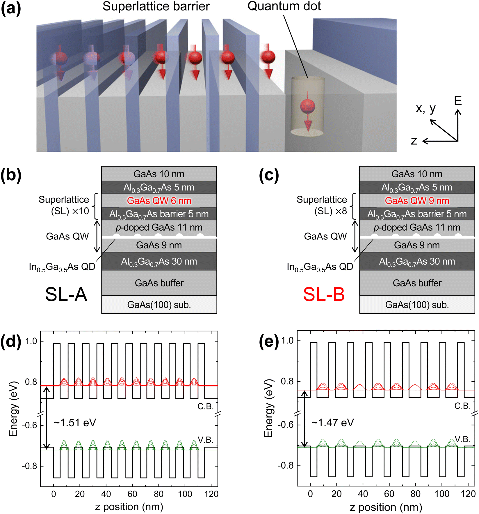 | ||
| Fig. 1 (a) Schematic illustration of spin-conserved electron transport from superlattice (SL) barrier to quantum dot (QD). Schematic sample structure of (b) SL-A with QW thickness of 6 nm and (c) SL-B with QW thickness of 9 nm. One-dimensional band calculation of GaAs/Al0.3Ga0.7As SL with electron and hole wavefunctions in the miniband for (d) SL-A and (e) SL-B. | ||
2. Experimental
2.1. Sample preparation
Schematic illustrations of two sample structures prepared by molecular beam epitaxy are shown in Fig. 1b and c. First, a 400-nm-thick GaAs buffer layer was grown on a semi-insulating GaAs(100) substrate. Then, a 30-nm-thick Al0.3Ga0.7As barrier layer was grown to confine photo-excited electrons and holes in the QD emissive layer. After the subsequent growth of a 9-nm-thick GaAs layer, a single layer of 7.5-ML-thick In0.5Ga0.5As QDs was grown at 773 K. The QDs were capped with an 11-nm-thick GaAs layer with Be doping (3 × 1017 cm−3) at the same temperature, followed by the growth of SL barriers. Notably, the In0.5Ga0.5As QDs were embedded in a 20-nm-thick GaAs QW. Such a dot-in-well structure enabled efficient carrier injection into the QDs.29 The SL barriers comprised 10 repeats of 6-nm-thick GaAs QW and 5-nm-thick Al0.3Ga0.7As barrier, or 8 repeats of 9-nm-thick GaAs QW and 5-nm-thick Al0.3Ga0.7As barrier. A 5-nm-thick Al0.3Ga0.7As layer was grown on the SL barrier and capped with a 10-nm-thick GaAs layer. The growth temperatures of the layers excluding the QDs and their capping layers were set to 853 K. Hereafter, samples with 6-nm-thick QW and 9-nm-thick QW SL layers are labeled SL-A and SL-B, respectively. The two samples exhibit similar SL barrier thicknesses.2.2. Optical characterization
Circularly polarized PL and time-resolved experiments were conducted at RT using a streak camera combined with a spectrometer under σ+-polarized excitation. The excitation energies were mainly changed from 1.39 to 1.59 eV, excluding those for PL excitation measurements. The excitation energies were set to 1.51 and 1.47 eV to selectively excite the SL heavy-hole states of SL-A and SL-B, respectively (Fig. 1d, e and 3b). Both the excitation and detection directions coincided with the sample growth direction. A mode-locked Ti:Sapphire pulsed laser with a repetition rate of 80 MHz, pulse width of <100 fs, and spectral width of 10 nm was used as the excitation source. The laser spot diameter was ∼50 μm. The full-width half maximum of the laser pulse time response curve was ∼11 ps. To characterize polarization-resolved optical properties, a linear polarizer and a quarter-wave plate were inserted into the excitation (detection) beam paths to generate (detect) circularly polarized excitation (emission). For this study, the spin polarization of electrons generated in the GaAs layers was expected to be 50% according to the optical selection rule when considering valence-band mixing. The circular polarization degree (CPD) of QD PL is defined as (Iσ+ − Iσ−)/(Iσ+ + Iσ−) using the circularly polarized PL intensity Iσ±, reflecting the spin polarization of electrons at QD emissive states. For PL excitation measurements at RT, a tunable Ti:Sapphire laser was used as the excitation source. In this study, the GaAs capping layer was p-doped to supply holes to the QDs. Furthermore, p-doping can lead to a hole-rich condition in the QDs. Therefore, PL and the CPD properties of QDs were expected to depend on the electron spins injected into the QDs. One-dimensional band structures of the SL and wavefunctions of electrons and holes were calculated using the nextnano software.303. Results and discussion
The high-angle annular dark-field scanning transmission electron microscopy images of the In0.5Ga0.5As QDs and GaAs/Al0.3Ga0.7As SL structures for SL-A and SL-B are shown in Fig. 2a and b, respectively. The results indicated the formation of atomically flat GaAs/Al0.3Ga0.7As interfaces. Sharp interfaces significantly reduced the interfacial roughness scattering of tunneling electrons, which suppressed spin relaxation by tunneling between adjacent GaAs QWs. Notably, electron tunneling time was expected to differ between the two samples. As the QW of SL-A was thinner than that of SL-B, the electron miniband energy was higher for SL-A (Fig. 1d and e). Consequently, the overlap of electron wavefunctions between adjacent QWs was stronger for SL-A, implying faster electron tunneling. Contrarily, weaker wavefunction overlap for SL-B facilitates radiative recombination of electrons and holes within QWs during PL measurements and reduces the efficiency of electron transport from SL to QDs. Buried In0.5Ga0.5As QDs are shown in Fig. 2a and b. As shown in the insets, the typical QD diameters/heights of SL-A and SL-B were estimated as 21/3.5 and 25/4.2 nm, respectively. The formation of differently sized QDs was attributed to time-varying growth conditions, such as growth rate and arsenic pressure. | ||
| Fig. 2 High-angle annular dark-field scanning transmission electron microscopy images of (a) SL-A and (b) SL-B, where the regions from the bottom Al0.3Ga0.7As layers to the SL layers are visible. The insets show typical high-resolution high-angle annular dark-field scanning transmission electron microscopy images of buried In0.5Ga0.5As QDs. | ||
 | ||
| Fig. 3 (a) Overview of PL spectra at an excitation energy above SL miniband. (b) PL excitation spectra detected at QD ground state. (c) QD PL spectra at excitations of GaAs QW and SL, where the PL intensities are normalized to the peak PL intensity at an excitation of GaAs QW. Normalized PL time profiles of QD excited states at excitations of GaAs QW and SL for (d) SL-A and (e) SL-B. The solid lines indicate the best-fitted rate equation results. | ||
An overview of the PL spectra of the two samples measured at excitation energies above the SL miniband states is shown in Fig. 3a. Four PL peaks were observed for both samples. PL peak energies of 1.23 and 1.20 eV for SL-A and SL-B originated from the QD ground states, respectively. The lower energy shift of SL-B was attributed to a large QD size, confirmed by scanning transmission electron microscopy observations. For QD PL from the first excited state, the PL peak energy was 1.26 eV for SL-B as compared to 1.29 eV for SL-A. Small PL peaks at 1.43 eV for both samples originated from the 20-nm-thick GaAs QWs surrounding the QDs. PL peak energies of 1.51 and 1.47 eV for SL-A and SL-B originated from SL miniband states, respectively. The PL excitation spectra detected in the QD ground states are shown in Fig. 3b, where distinct features related to the heavy-hole and light-hole states are observed. The heavy hole energies of SL-A and SL-B were located at 1.51 and 1.47 eV, respectively. The values were consistent with the band-calculation results shown in Fig. 1d and e. The obtained PL/PL excitation results provided experimental evidence of SL structures designed with sharp GaAs/Al0.3Ga0.7As interfaces. Furthermore, different intensity ratios of QD PL to SL PL of the two samples are shown in Fig. 3a. A stronger SL PL of SL-B compared to that of SL-A was related to a smaller wavefunction penetration into adjacent QWs. For SL-B, the dominant radiative recombination within SL reduced the electron transport efficiency, resulting in a lower QD PL intensity. The QD PL spectra at the excitation of a 20-nm-thick GaAs QW and SL miniband are shown in Fig. 3c. The PL intensities were normalized to the peak PL intensity at the GaAs QW excitation. For both samples, the QD PL intensity increased significantly upon excitation of the SL miniband relative to the excitation of the GaAs QW. The increase was slightly greater for SL-A. Considering that the total thickness of the SL-QW layers to be excited was greater for SL-B, the obtained result supported a lower electron transport efficiency.
The difference in electron transport properties between the two samples was observed from the time-dependent PL behavior. The normalized PL time profiles of the QD excited states for SL-A and SL-B are shown in Fig. 3d and e, respectively, measured at the excitations of the GaAs QWs and SL minibands. At SL miniband excitation, a slower PL increase was observed for SL-B than for SL-A. To examine the electron transport time (τtr), rate equation analysis of the PL time profiles was performed (details are provided in Supplementary note S1, ESI†). The same value of τtr = 11 ps was obtained at an excitation of GaAs QW, whereas τtr = 21 ps for SL-B was longer than τtr = 14 ps for SL-A at SL miniband excitation. The longer τtr for SL-B was related to slower electron tunneling between adjacent QWs of the SL, as aforementioned. Conversely, the significant increase in τtr from 11 to 21 ps indicated the contribution of electrons generated in the SL far from the QDs to the QD light emission. For SL-A, τtr at SL excitation was close to that at GaAs QW excitation. Thus, fast electron tunneling was observed between the adjacent QWs of SL. Here, note that no significant difference in the electron transport efficiency between the two samples could occur from the perspective of electrical carrier injection. In PL measurements, holes were generated in the GaAs QW of SL; thus, electrons radiatively recombined with holes during transport. The radiative recombination reduced electron transport efficiency, particularly for SL-B. However, for a p–i–n LED using SL as an electron transport layer, electrons and holes were transported from the opposite direction to the active layer. Thus, radiative recombination within the SL was almost negligible and cannot affect the electron transport efficiency.
Further, the electron spin transport from the SL to the QDs was analyzed. The circularly polarized PL time profiles and the corresponding CPD of the QD excited states for SL-A and SL-B are shown in Fig. 4a and b, respectively, measured upon excitation of the SL miniband. The CPD values during the initial time are shown in the insets. The initial CPD properties of the QD excited states reflected the degree of spin relaxation during transport to QDs.22,31 Although the heavy-hole and light-hole states were split, as shown in Fig. 3b, the initial spin polarization of electrons generated in the SL was estimated as 50% when considering the valence-band mixing and spectral width of the excitation pulsed laser.22,23 The initial CPD value of SL-B was higher than that of SL-A. The initial CPD values as a function of the excitation energy are plotted in Fig. 4c. For this study, initial CPD is defined as the mean value near a CPD peak in the initial time region. At GaAs QW excitation, identical values of 26–27% were obtained for the two samples. The values were close to the previously reported values for electron spin injection from the GaAs barrier into InGaAs QDs.29,32,33 Furthermore, the initial CPD value was dependent on the excitation energy. The value increased to 32% under SL excitation for SL-A, while a significant increase to 37% for SL-B was observed. The results indicated the efficient transport of spin-polarized electrons from SL to QDs while maintaining a high spin polarization for SL-B. Notably, the time-dependent QD PL at SL excitation included electron spin transport from both the GaAs QW around the QDs and the SL. Each component needs to be separated to extract the net spin polarization of the electrons transported from SL to QDs.
 | ||
| Fig. 4 Circularly polarized PL time profiles and corresponding CPD of QD excited states for (a) SL-A and (b) SL-B, at SL miniband excitation. The insets show the CPD time profiles in the initial time region. The black solid lines indicate the best-fitted rate equation results, which are decomposed into two components, spin-polarized carriers generated in GaAs QW and SL. (c) Initial PL CPD of QD excited states as a function of excitation energy. (d) Schematic model of spin-split rate equation, where the electron spin transport to the QD from the GaAs QW and the SL is considered. | ||
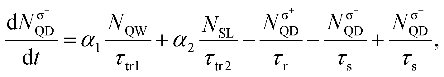
To separate the electron spin transport from the GaAs QW and SL, rate equation analysis was performed considering two spin transport processes, as schematically illustrated in Fig. 4d. This rate equation model was employed to extract the net spin polarization of the electrons transported from SL to QDs, because the raw time-dependent circularly polarized PL data of the QDs screen the spin polarization properties of transported electrons. The initial number of excitons generated in the GaAs QW (SL) with σ+-polarization was expressed by N1(2). The rate equation was expressed as:
 | (1) |
 | (2) |
 | (3) |
 | (4) |
| τ tr1 (ps) | α 1 | τ tr2 (ps) | α 2 | τ r (ps) | τ s (ps) | N 2/N1 | |
|---|---|---|---|---|---|---|---|
| SL-A | 11 | 0.67 | 41 | 0.72 | 248 | 120 | 1.61 |
| SL-B | 11 | 0.67 | 80 | 0.76 | 258 | 120 | 1.49 |
To reveal the origin of the difference in electron spin transport between SL-A and SL-B, the spin relaxation of the SL was investigated. The time-dependent PL CPD of the SL miniband with the single-exponential decay fittings is shown in Fig. 5a. Excitation energies of 1.71 and 1.60 eV were used for SL-A and SL-B, respectively, to excite the second miniband. The initial CPD of SL PL was approximately 27%, whereas the CPD decay properties differed significantly between the two samples. A much longer spin relaxation time τs = 195 ps was obtained for SL-B as compared to τs = 71 ps for SL-A. The difference in τs was interpreted based on the electron confinement energy (E1e). The spin relaxation time obtained as a function of E1e is plotted in Fig. 5b. The least squares fit resulted in τs ∝ E−201e, which agreed with the dependence of the spin relaxation time on the electron confinement energy expected in D’yakonov–Perel’ theory of QW.20,34 Therefore, the spin relaxation time of SL was dependent on the D’yakonov–Perel’ interaction, and the smaller electron confinement energy in the QW led to a longer spin relaxation time. Thus, the spin-relaxation time of SL at RT could be controlled by changing the QW thickness.
 | ||
| Fig. 5 (a) Time-dependent CPD of SL PL with single-exponential decay fittings (solid lines) for SL-A and SL-B. (b) Spin relaxation time (τs) as a function of electron confinement energy (E1e) for SL-A and SL-B. The solid line showing τs ∝ E−2.01e is fitted using the least square method. The dashed and dotted lines showing τs ∝ E−1.51e and τs ∝ E−2.51e through the data point of SL-A are also shown to justify the fitting result, τs ∝ E−2.01e. (c) Schematic illustration of electron spin transport dynamics in GaAs QW and SL under the σ+-polarized excitation of SL miniband. | ||
Finally, the electron spin transport dynamics of SL-B with the σ+-polarized excitation of SL were explored. Under the excitation conditions, the GaAs layers around QDs and SL were excited together, as depicted in Fig. 5c. The spin polarization of electrons injected from the i-GaAs barrier into the QDs via the wetting layer was expected to be low owing to the rapid spin relaxation in GaAs at RT.35 The results reflected an initial CPD of 26–27% at GaAs QW excitation (Fig. 4c). Contrarily, the spin polarization of electrons transported from the SL to the QDs via p-GaAs capping layer cannot be degraded for the following two reasons. First, spin-polarized electrons can be transported from the SL to the QDs before promoting spin relaxation. The deduced electron transport time, τtr2 = 80 ps, was faster than the spin relaxation time of the SL, τs = 195 ps. The net electron transport time should be faster because τtr2 includes the transport time from p-GaAs to QDs. It is also possible that the obtained τtr2 is overestimated. In these PL measurements, electrons and holes were generated in the SL. In general, hole transport is slower than electron transport because of its higher effective mass. As a result, the QD PL rise time, which is closely related to τtr2, could be determined by the slower hole transport. In this case, the net electron transport time should be much shorter than the spin-relaxation time. We expect the second advantage to be the use of p-doped GaAs capping layer. A previous study of p-doped InGaAs QDs demonstrated that D’yakonov–Perel’ spin relaxation in the p-doped GaAs capping layer can be suppressed at RT through electron-impurity scattering.17,36 Therefore, we conclude that the combination of electron transport before the promotion of spin relaxation in the SL and suppressed spin relaxation in the p-doped GaAs capping layer results in spin-conserved electron transport from the SL to the QDs even at RT. Future investigations of electron spin transport properties under the application of an electric field will provide valuable insights into the applicability of SL to electron spin transport layers of spin-polarized LEDs and lasers.
4. Conclusions
In summary, the electron spin transport from a GaAs/Al0.3Ga0.7As SL barrier to In0.5Ga0.5As QDs was studied at RT through a combination of time-resolved circularly polarized PL and rate equation analysis, separating the two transport processes from the GaAs QW around the QDs and from the SL. The electron transport time in the SL depends on the QW thickness. As the QW thickness increases, the electron transport time increases because of the weaker wavefunction overlap between adjacent QWs. We also found that the degree of spin-polarization conservation during transport depended on the QW thickness. Rate equation analysis demonstrated that electrons could be transported from the SL to the QDs while maintaining a high spin polarization even at RT. The achieved spin-conserved electron transport can be attributed to the combination of electron transport, which is sufficiently faster than spin relaxation in the SL, and the suppression of spin relaxation in the p-doped GaAs layer capping the QDs.Data availability
The data that support the findings of this study are available from the corresponding authors upon reasonable request.Author contributions
S. Hiura and A. M. conceived the idea and designed the experiments. S. Hatakeyama prepared the samples by MBE. S. Hiura and S. Hatakeyama performed circularly polarized PL and time-resolved experiments and analyzed the data with the assistance of J. T. PL excitation experiments and data analysis were conducted by M. J. under the supervision of I. B. and W. C. J. T. performed scanning transmission electron microscopy experiments and analyzed the data. S. H. wrote the manuscript. All the authors reviewed and provided feedback on the manuscript.Conflicts of interest
There are no conflicts to declare.Acknowledgements
This work was financially supported by JSPS KAKENHI (Grant No. JP16H06359, JP21H01356, JP21KK0068, JP23K26153, JP24K00913), JST FOREST (Grant No. JPMJFR202E), JST ALCA-Next (Grant No. JPMJAN23E5), Swedish Foundation for International Cooperation in Research and Higher Education (STINT) (Grant No. JA2014-5698), and Advanced Technology Institute Research Grants 2021. A part of this work was conducted at Joint-Use Facilities: Laboratory of Nano-Micro Material Analysis and High-Voltage Electron Microscope Laboratory, supported by “Nanotechnology Platform Program” and “Advanced Research Infrastructure for Materials and Nanotechnology in Japan (ARIM)” of the Ministry of Education, Culture, Sports, Science and Technology (MEXT), Grant Number JPMXP1222HK0049 (Hokkaido University).References
- Y. Huang, V. Polojärvi, S. Hiura, P. Höjer, A. Aho, R. Isoaho, T. Hakkarainen, M. Guina, S. Sato, J. Takayama, A. Murayama, I. A. Buyanova and W. M. Chen, Nat. Photonics, 2021, 15, 475–482 CrossRef CAS.
- R. Farshchi, M. Ramsteiner, J. Herfort, A. Tahraoui and H. T. Grahn, Appl. Phys. Lett., 2011, 98, 162508 CrossRef.
- P. A. Dainone, N. Figueiredo Prestes, P. Renucci, A. Bouché, M. Morassi, X. Deveaux, M. Lindemann, J.-M. George, H. Jaffrès and A. Lemaître, et al. , Nature, 2024, 627, 783 CrossRef CAS PubMed.
- S. Hiura, Nature, 2024, 627, 737 CrossRef CAS PubMed.
- A. V. Khaetskii and Y. V. Nazarov, Phys. Rev. B: Condens. Matter Mater. Phys., 2000, 61, 12639–12642 CrossRef CAS.
- J. M. Elzerman, R. Hanson, L. H. Willems van Beveren, B. Witkamp, L. M. K. Vandersypen and L. P. Kouwenhoven, Nature, 2004, 430, 431–435 CrossRef CAS PubMed.
- M. Kroutvar, Y. Ducommun, D. Heiss, M. Bichler, D. Schuh, G. Abstreiter and J. J. Finley, Nature, 2004, 432, 81–84 CrossRef CAS PubMed.
- M. Sugawara and M. Usami, Nat. Photonics, 2009, 3, 30–31 CrossRef CAS.
- S. Chen, W. Li, J. Wu, Q. Jiang, M. Tang, S. Shutts, S. N. Elliott, A. Sobiesierski, A. J. Seeds and I. Ross, et al. , Nat. Photonics, 2016, 10, 307 CrossRef CAS.
- A. Jaffal, W. Redjem, P. Regreny, H. S. Nguyen, S. Cueff, X. Letartre, G. Patriarche, E. Rousseau, G. Cassabois, M. Gendry and N. Chauvin, Nanoscale, 2019, 11, 21847–21855 RSC.
- E. T. Hughes, C. Shang, J. Selvidge, D. Jung, Y. Wan, R. W. Herrick, J. E. Bowers and K. Mukherjee, Nanoscale, 2024, 16, 2966–2973 RSC.
- S. Chakrabarti, M. A. Holub, P. Bhattacharya, T. D. Mishima, M. B. Santos, M. B. Johnson and D. A. Blom, Nano Lett., 2005, 5, 209–212 CrossRef CAS PubMed.
- C. H. Li, G. Kioseoglou, O. M. J. van’t Erve, M. E. Ware, D. Gammon, R. M. Stroud, B. T. Jonker, R. Mallory, M. Yasar and A. Petrou, Appl. Phys. Lett., 2005, 86, 132503 CrossRef.
- L. Lombez, P. Renucci, P. F. Braun, H. Carrère, X. Marie, T. Amand, B. Urbaszek, J. L. Gauffier, P. Gallo and T. Camps, et al. , Appl. Phys. Lett., 2007, 90, 2005–2008 CrossRef.
- F. Cadiz, A. Djeffal, D. Lagarde, A. Balocchi, B. Tao, B. Xu, S. Liang, M. Stoffel, X. Devaux and H. Jaffres, et al. , Nano Lett., 2018, 18, 2381–2386 CrossRef CAS PubMed.
- A. E. Giba, X. Gao, M. Stoffel, X. Devaux, B. Xu, X. Marie, P. Renucci, H. Jaffrès, J.-M. George and G. Cong, et al. , Phys. Rev. Appl., 2020, 14, 034017 CrossRef CAS.
- K. Etou, S. Hiura, S. Park, K. Sakamoto, J. Takayama, A. Subagyo, K. Sueoka and A. Murayama, Phys. Rev. Appl., 2021, 16, 014034 CrossRef CAS.
- K. Etou, S. Hiura, S. Park, J. Takayama, A. Subagyo, K. Sueoka and A. Murayama, Phys. Rev. Appl., 2023, 19, 024055 CrossRef CAS.
- M. I. D’yakonov and V. I. Perel, Zh. Eksp. Teor. Fiz., 1973, 65, 362 Search PubMed . Optical orientation in a system of electrons and lattice nuclei in semiconductors. Theory Sov. Phys. JETP, 1974, 38, 177.
- R. S. Britton, T. Grevatt, A. Malinowski, R. T. Harley, P. Perozzo, A. R. Cameron and A. Miller, Appl. Phys. Lett., 1998, 73, 2140–2142 CrossRef CAS.
- M. I. Miah, J. Phys. D: Appl. Phys., 2008, 41, 035105 CrossRef.
- S. Hiura, K. Itabashi, K. Takeishi, J. Takayama, T. Kiba and A. Murayama, Appl. Phys. Lett., 2019, 114, 072406 CrossRef.
- S. Hiura, S. Hatakeyama, J. Takayama and A. Murayama, Appl. Phys. Lett., 2020, 116, 262407 CrossRef CAS.
- Y. Ohno, S. Iba, R. Okamoto, Y. Obata, K. Obu, J. J. P. Domingez and H. Saito, Appl. Phys. Express, 2020, 13, 123003 CrossRef CAS.
- S. Iba, R. Okamoto, K. Obu, Y. Obata and Y. Ohno, Micromachines, 2021, 12, 1112 CrossRef PubMed.
- A. Tackeuchi, Y. Nishikawa and O. Wada, Appl. Phys. Lett., 1996, 68, 797–799 CrossRef CAS.
- A. Tackeuchi, T. Kuroda, S. Nishikawa and O. Wada, Jpn. J. Appl. Phys., 1999, 38, 4680 CrossRef CAS.
- A. Malinowski, R. S. Britton, T. Grevatt, R. T. Harley, D. A. Ritchie and M. Y. Simmons, Phys. Rev. B: Condens. Matter Mater. Phys., 2000, 62, 13034–13039 CrossRef CAS.
- S. Hiura, M. Takishita, J. Takayama, S. Sato and A. Murayama, Phys. Rev. Appl., 2020, 14, 044011 CrossRef CAS.
- S. Birner, T. Zibold, T. Andlauer, T. Kubis, M. Sabathil, A. Trellakis and P. Vogl, IEEE Trans. Electron Devices, 2007, 54, 2137–2142 CAS.
- H. Kise, S. Hiura, S. Park, J. Takayama, K. Sueoka and A. Murayama, Appl. Phys. Lett., 2023, 122, 232405 CrossRef CAS.
- S. Park, S. Hiura, J. Takayama, K. Sueoka and A. Murayama, Adv. Electron. Mater., 2022, 8, 2200588 CrossRef CAS.
- S. Park, S. Hiura, H. Kise, J. Takayama, K. Sueoka and A. Murayama, Nanoscale, 2023, 15, 16784–16794 RSC.
- M. I. D’yakonov and V. Y. Kachorovski, Sov. Phys. Semicond., 1986, 20, 110 Search PubMed.
- S. Oertel, J. Hübner and M. Oestreich, Appl. Phys. Lett., 2008, 93, 132112 CrossRef.
- S. Sato, S. Hiura, J. Takayama and A. Murayama, Appl. Phys. Lett., 2008, 116, 182401 CrossRef.
Footnote |
| † Electronic supplementary information (ESI) available. See DOI: https://doi.org/10.1039/d4cp03973d |
| This journal is © the Owner Societies 2025 |