
A density functional theory study of two-dimensional bismuth selenite: layer-dependent electronic, transport and optical properties with spin–orbit coupling†
Yao
Wang‡
 ab,
Jinsen
Zhang‡
a,
Xuanlin
Zhang
d,
Chenqiang
Hua
*c,
Yunhao
Lu
d and
Xinyong
Tao
a
ab,
Jinsen
Zhang‡
a,
Xuanlin
Zhang
d,
Chenqiang
Hua
*c,
Yunhao
Lu
d and
Xinyong
Tao
a
aCollege of Materials Science and Engineering, Zhejiang University of Technology, Hangzhou 310014, China. E-mail: wangyao@zjut.edu.cn; 2112025100@zjut.edu.cn; tao@zjut.edu.cn
bMoganshan Research Institute at Deqing County Zhejiang University of Technology, Huzhou 313000, China
cHangzhou International Innovation Institute, Beihang University, Hangzhou 311115, China. E-mail: huachenqiang@buaa.edu.cn
dSchool of Physics, Zhejiang University, Hangzhou 310027, China. E-mail: 11926054@zju.edu.cn; luyh@zju.edu.cn
First published on 3rd December 2024
Abstract
Recently, atomic-thickness van der Waals (vdW) layered bismuth selenite (Bi2SeO5) has been successfully synthesized, not only expanding the family of two-dimensional (2D) materials, but also playing a pivotal role in the advancement of 2D electronics as a high-κ dielectric. In this work, we systematically study the basic properties of 2D Bi2SeO5 through first-principles calculations, focusing on the spin–orbit coupling (SOC) effect and layer-dependent behaviors. The results show that SOC can adjust the bandgap of bulk/2D Bi2SeO5 from direct to indirect, with the bandgap decreasing upon increasing the thickness due to quantum confinement. Importantly, we observe that SOC has a negligible effect on the valence band edge but significantly impacts the conduction band edge, due to the specific distribution of the Bi-p orbital. We also explore the vdW magnetic tunneling junction based on 2D Bi2SeO5, which can exhibit significant tunneling magnetoresistance between the parallel and antiparallel magnetic alignments of electrodes, e.g. 900% for 1L and 1800% for 2L. As for the optical properties, strong layer dependence is also verified, and the large absorption coefficient is determined to be ∼106 cm−1. At last, we also explore the piezoelectric properties. Overall, layered Bi2SeO5 is a potential candidate material for electronic device and optoelectronic applications, as well as nano-spintronic applications.
1. Introduction
Spin–orbit coupling (SOC), a fundamental quantum mechanical interaction between the spin and orbital angular momentums, plays a pivotal role in determining the electronic structure, optical properties, and transport phenomena in materials.1–4 Specifically, SOC can induce profound modifications in band structures, manifesting as phenomena such as spin splitting, spin scattering and band inversion, etc.,5–7 rendering materials with strong SOC particularly promising for next-generation optoelectronic, spintronic, and quantum computing applications.8,9 Van der Waals (vdW) layered materials have emerged as a revolutionary platform for materials science research in recent decades.10–14 A distinctive advantage of vdW materials lies in their atomically precise surfaces characterized by the absence of dangling bonds, exceptional thickness uniformity, and atomically smooth interfaces-properties that markedly distinguish them from conventional three-dimensional materials.15 Remarkably, vdW systems always show the layer-dependent properties when the thickness is confined to sub-nanometer (few-layer). The interplay between SOC and quantum confinement effects in ultrathin vdW materials offers unprecedented opportunities to engineer their electronic structure and transport properties with atomic-layer precision, which establishes a versatile platform for designing next-generation multifunctional materials with precisely tailored properties, enabling transformative advances in quantum technology, optoelectronics, and spintronics.16–18Very recently, large-scale two-dimensional (2D) bismuth selenite (Bi2SeO5) with a high dielectric constant has been achieved through layer-by-layer oxidation or exfoliation.19–21 Layered Bi2SeO5 was reported to have a large bandgap and as a high-κ dielectric, it can show improved electronic performance compared to 2D materials such as Bi2O2Se, MoS2, and graphene due to suppression of the current leakage.22 SOC plays a pivotal role in the electronic structure, and thus, it may be important for Bi-based system. In addition, as a vdW material, the layer-dependent properties have not been studied yet, including the electronic, transport, optical, and piezoelectric properties, etc. Therefore, an in-depth study is necessary.
In this paper, the geometric, electronic, transport, optical, and piezoelectric properties of bulk/2D Bi2SeO5 are investigated using density functional theory (DFT). The cleavage energy is 31.87 meV Å−2, indicating the experimental exfoliation feasibility. The band calculations exhibit that the bandgap decreases from 3.06 to 2.79 eV with an exponential tendency, and SOC will further reduce the bandgap by ∼0.3 eV. Interestingly, it is found that the valence band (VB) edge is dominated by the O-p orbital, and Bi-p contributes obviously to the conduction band (CB) edge. As a result, SOC mainly affects the CBs while leaves the VBs intact, which is quite different from the normal metal compounds. Next, we construct a vdW FeS2/Bi2SeO5/FeS2 magnetic tunneling junction (MTJ) and it shows significant tunneling magnetoresistance (TMR). The optical properties of 2D Bi2SeO5 show obvious layer dependence and SOC modulation, and large absorption coefficients (∼106 cm−1) are also observed. Finally, we show that bulk/2D Bi2SeO5 has broken inversion symmetry, and possibly has potential for piezoelectric applications. Our study not only reveals that SOC is both intriguing and significant for Bi2SeO5, but also highlights the layer-dependent electronic, optical, and piezoelectric properties of 2D Bi2SeO5, emphasizing its potential applications in spintronics.
2. Computational methods
We performed first-principles calculations using the Vienna Ab initio Simulation Package (VASP) to describe the exchange–correlation potential by the generalized gradient approximation (GGA) of Perdew–Burke–Ernzerhof (PBE).23–25 The interactions between the nuclear and valence electrons were described by the projected augmented wave (PAW) potential, with an energy-cutoff of 520 eV for the plane-wave basis. A 3 × 2 × 6/2 × 6 × 1 k-point mesh was used to sample the Brillouin zone (BZ) of primitive bulk/2D Bi2SeO5. To avoid the interactions between the periodic images perpendicular to the basal plane, we included a vacuum space of 20 Å. We tested different vdW interactions and chose the optB86b exchange functional (optB86b-vdW).26 The systems were optimized with a force threshold of 10−3 eV Å−1 and the energy convergence criterion was set to be 10−6 eV. SOC was included due to the heavy element Bi.27 A hybrid-exchange functional (HSE06)28 with the PBE functional was used to compare the band structure.In order to obtain more information about the transport properties of 2D Bi2SeO5, we investigated its relaxation time (τ) based on the Bardeen–Shockley deformation potential (DP) theory for 2D materials:29,30
 | (1) |
We used double-zeta polarization function (DZP) to initialize the Kohn–Sham states and adopted the nonequilibrium Green's function (NEGF-DFT) to calculate the transmission properties. The corresponding energy cutoff was set to be 80 Hartee. Then, the k-point meshes of the scattering region and the electrode were set to 4 × 11 × 1 and 4 × 11 × 100, respectively. The energy convergence criteria for both self-consistent calculations and transmission spectrum calculations were consistently set to 10−5 eV. Transmission spectra were calculated using Nanodcal31 and Atomistic ToolKit32,33 software.
The linear optical properties can be derived from its complex dielectric function, providing crucial insights into its applicability in advanced optoelectronic technologies:
| ε(ω) = ε1(ω) + iε2(ω), | (2) |
 | (3) |
 | (4) |
 | (5) |
3. Results and discussion
3.1 Geometric and electronic properties of bulk/2D Bi2SeO5
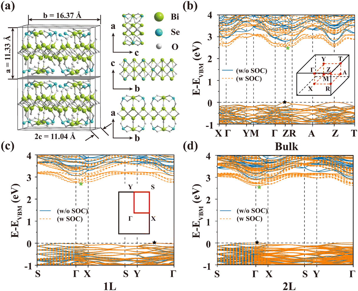 | ||
| Fig. 1 (a) Crystal structure of bulk Bi2SeO5. The vdW gap is marked with a gray plane, reflecting the cleavage position. Electronic band structures of (b) bulk, (c) 1L and (d) 2L Bi2SeO5 with SOC (orange dashed lines). For easy comparison, we plot the bands without SOC together (blue solid lines). Green and black pentagrams represent the CBM and VBM, respectively. Inset: The Brillouin zones of (b) bulk and (c) 2D Bi2SeO5 with high symmetry points and lines. | ||
| System | a (Å) | b (Å) | c (Å) | V (Å3) |
|---|---|---|---|---|
| Exp. | 11.44 | 16.28 | 5.49 | 1022.48 |
| DFT-D3BJ | 11.37 | 16.41 | 5.52 | 1029.93 |
| dDsC | 11.38 | 16.43 | 5.52 | 1032.09 |
| optB88-vdW | 11.37 | 16.44 | 5.54 | 1035.55 |
| optB86b-vdW | 11.33 | 16.37 | 5.52 | 1023.81 |
| rev-vdW-DF2 | 11.35 | 16.40 | 5.53 | 1029.35 |
As shown in Fig. 1b, we find that bulk Bi2SeO5 is a semiconductor with a direct bandgap of 2.79 eV at the Z point, which is consistent with the previous calculations21 and also suitable for ultraviolet optoelectronic devices.40,41 We also use the HSE06 functional to compare the band structure, which also has a direct bandgap (of 3.87 eV), as shown in Fig. S1a (ESI†). Near the conduction band minimum (CBM) and valence band maximum (VBM), i.e. the Z point, the effective mass is calculated to be 0.397 m0 [electron effective mass (me)]/5.345 m0 [hole effective mass (mh)] along the Z–T direction, reflecting that the top VB is weakly dispersed (see Fig. 1b). Here m0 represents the electron mass. In addition, the calculated values of effective mass are 1.431 m0 (me)/0.998 m0 (mh) along the Z–Γ direction, and 0.776 m0 (me)/1.580 m0 (mh) along the Z–R direction, respectively. These results are comparable to those of some typical 2D materials, such as MoS2 (0.48 m0)42 and h-BN (0.99 m0).43
We also plot the local density of states (LDOS) in Fig. 2a. It is found that the VBs are dominated by the O-p orbital, and the contribution of the Bi-p orbital becomes the largest near the CBM. Such a behavior is different from that of normal metal compounds, in which the s orbital of the metal is not negligible near the CBM.44 In Fig. 2a, we present a detailed plot of the partial density of states (PDOS), revealing that the py and pz orbitals of Bi have nearly equal contribution, both of which are significantly larger than the Bi-px orbital. This suggests that the interlayer interaction in this compound effectively mixes the out-of-plane and in-plane orbitals [see the spatial distribution of wavefunction for the lowest CBs in Fig. S2a–c (ESI†)].
 | ||
| Fig. 2 (a)–(c) The LDOS and PDOS of bulk/1L/2L Bi2SeO5, respectively. The p orbitals of Bi, Se and O are projected in the LDOS and the px, py, and pz orbitals of Bi are projected in the PDOS. Note that the directions of px, py, and pz for the bulk system correspond to the b, c, and a directions (see Fig. 1a). | ||
 | (6) |
Typically, the thickness has a significant influence on the basic properties of layered systems due to the quantum confinement.47 For instance, single-layer MoS2/MoSe2 has a direct bandgap while multilayer systems have indirect bandgaps.48,49 Therefore, we further investigate the layer-dependent electronic properties of 2D Bi2SeO5, and several results are summarized in Table 2. For example, the in-plane lattice constants gradually increase by 0.04 Å when reducing the thickness from the bulk to 1L Bi2SeO5, which can be ascribed to the decreased interlayer interaction. The bandgap variation under the quantum confinement effect is also discussed and verified [see Note S1 and Fig. S3 (ESI†)].
| System | a (Å) | b (Å) | Bandgap (eV) | Type | Bandgap-SOC (eV) | Type |
|---|---|---|---|---|---|---|
| 1L | 16.41 | 5.48 | 3.06 | Indirect | 2.73 | Indirect |
| 2L | 16.39 | 5.49 | 2.91 | Direct | 2.62 | Indirect |
| 3L | 16.38 | 5.51 | 2.85 | Direct | 2.59 | Indirect |
| Bulk | 16.37 | 5.52 | 2.79 | Direct | 2.55 | Indirect |
Fig. 1c and d display the band structures of 1L and 2L Bi2SeO5 [see 3L in Fig. S4 (ESI†)]. In the 2D limit, the initial Z point of 3D BZ folds back to the Γ point. The VBM for 1L Bi2SeO5 is 27.21 meV above the Γ point, which is located in the Y–Γ direction; while the CBM is much close to the Γ point, leading to an indirect bandgap of 3.06 eV [4.18 eV using the HSE06 functional (see Fig. S1b ESI†)]. When interlayer interactions are naturally included for the multilayer Bi2SeO5, the bandgap becomes direct and the values range from 2.91 to 2.85 eV for 2L and 3L systems (see Table 2).
To visualize the interlayer interaction, the LDOS and PDOS of 1L and 2L Bi2SeO5 are also calculated as shown in Fig. 2b and c. Similar to the bulk case, VBs are dominated by the O-p orbital. We also found that the Bi-p orbital has obvious contribution to CBs. For 1L Bi2SeO5, the pz-orbital dominates while for 2L Bi2SeO5, pz and py orbitals have nearly equal contributions near the CBM mimicking the bulk case. This orbital redistribution phenomenon is directly related to the interlayer interaction, which directly entangles the in-plane orbitals with the out-of-plane pz orbital. As a result, the bonding and antibonding like charge distribution is formed and the proportion of the pz orbital decreases near the CBM [see Fig. S2d–f (ESI†)], demonstrating the orbital mixing and redistribution.
Subsequently, we explore the SOC effect on the electronic properties of 2D Bi2SeO5. The results of the band structures are plotted in Fig. 1b–d. It can be seen that SOC also leads to the reduction of the bandgap. For example, the bandgap exhibits a strong layer-dependent evolution, decreasing from 3.06 to 2.73 eV for 1L Bi2SeO5, from 2.91 to 2.62 eV for 2L Bi2SeO5, and from 2.85 to 2.59 eV for 3L Bi2SeO5 [also see Fig. S4 (ESI†)]. In the absence of SOC, 2D Bi2SeO5 systems are direct bandgap semiconductors except for 1L Bi2SeO5. However, under the effect of SOC, the CBM is lightly shifted from Γ, and 2D Bi2SeO5 becomes an indirect bandgap semiconductor regardless of the layer number (see Table 2). Furthermore, as shown in Fig. 2b and c, the Bi-p orbital in 2D Bi2SeO5 also has a significant contribution to the CBs. Therefore, under the influence of SOC, the CBs are pulled down obviously, leading to a decrease of the bandgap.
Besides, the introduction of SOC will lead to a change in effective mass, especially the me since SOC mainly affects CBs, as shown in Fig. S5 (ESI†). Taking 1L Bi2SeO5 as an example, the magnitude of me is 0.447 m0 along the Γ–X direction and 0.458 m0 along the Γ–Y direction without the inclusion of SOC, exhibiting a relatively isotropic behavior. With SOC, me increases significantly along both the Γ–X and Γ–Y directions. For 2L/3L Bi2SeO5, when SOC is considered, the magnitude of me also increases along the Γ–X and Γ–Y directions. As the layer number increases from 1L to 3L Bi2SeO5, the in-plane anisotropy of me becomes more pronounced, probably due to the interlayer interaction, which mixes the in-plane and out-of-plane p orbitals. As for mh, the impact of SOC is generally minimal [see Fig. S5b and d (ESI†)]. All results above demonstrate that SOC has a crucial influence on the electronic properties of Bi2SeO5.
With a moderate me, we then estimate the electrical conductivity (σ) of 1L Bi2SeO5 for electrons, as shown in Fig. S6 (ESI†). Due to the relaxation time approximation, we need to determine the τ of electrons. Using the DP theory, τ values are determined to be 63.56 and 114.07 fs along the x and y directions, respectively, which manifesting the strong anisotropy.56 Therefore, σ of electron for 1L Bi2SeO5 is about 0.90 and 1.62 × 10³ Ω−1 m−1 along the x and y directions with a carrier concentration of 1011 cm−2, which are comparable to those of some 2D materials.57,58 To demonstrate the anisotropy in 2D Bi2SeO5, we also estimate the τ of h along the x and y directions, which are determined to be 502.10 and 770.97 fs, respectively.
3.2 Bi2SeO5 based tunneling junction
After that, we turn to the transport properties of Bi2SeO5 based tunneling junctions because of the uniform surface of vdW layers and strong SOC.52,59,60 The transport device model is depicted in Fig. 3a and a nonmagnetic electrode is used firstly. We calculate the transmission properties of 1L/2D Bi2SeO5 (details in methods), and the zero-bias transmission spectra are shown in Fig. 3b and S7a (ESI†). One can find a large transmission gap near the Fermi energy due to the bandgap of 2D Bi2SeO5, indicating that the transmission in this region is forbidden with zero-bias. Beyond this region, the transmission probability gradually increases. Fig. 3b and S7a (ESI†) also illustrates the impact of SOC on the transmission rate. With SOC, the scattering probability near the CBM is substantially modulated, which is consistent with the band structure (see Fig. 1). Fig. 3b and S7a (ESI†) also exhibit the trend of transmission with different thickness of scattering region. For example, stacking one more layer on single-layer Bi2SeO5 will obviously enhance the scattering probability, thus reducing the transmission rate. All these results suggest that SOC is also important in the Bi2SeO5 based tunneling junctions and thus, one can make other kinds of tunneling junctions, where SOC is crucial. Besides, Bi2SeO5 based tunneling junction can be fabricated in future experiments to study the layer-dependent transmission phenomenon. | ||
| Fig. 3 (a) and (b) Schematic diagram and transmission spectra of the Al/1L Bi2SeO5/Al device. (c) and (d) Schematic diagram and transmission spectra of the FeS2/1L Bi2SeO5/FeS2 MTJ. | ||
Since SOC also plays a significant role in the MTJs,61,62 we then make a device using FeS2/Bi2SeO5/FeS2 layers, as shown in Fig. 3c, which can be used to explore the magnetic tunneling properties. Typically, MTJs exhibit high/low conductance when two ferromagnetic electrodes have the parallel/antiparallel magnetic configurations (PC/APC), due to the relative alignment of magnetization directions. The relative difference between the PC and APC configurations can be defined as the TMR, which is calculated using the formula:
 | (7) |
3.3 Optical properties of bulk/2D Bi2SeO5
The electronic structures of bulk/2D Bi2SeO5, which feature a significant contribution from p-orbitals in the conduction bands of bismuth, play a crucial role in defining their distinctive optical properties. This unique electronic configuration allows for the manipulation of optical behaviors in Bi2SeO5, minimizing the dependence on sp-hybridization. As a result, Bi2SeO5 emerges as a promising candidate for both optoelectronic and electronic applications.65 The dielectric properties of Bi2SeO5 have been calculated across an energy range from 0 to 12 eV.As shown in Fig. 4a–h, the optical properties of bulk/2D Bi2SeO5 are essentially equivalent along the xx and yy directions. Therefore, subsequent analyses focus solely on the optical properties along the xx direction. The calculated spectra of ε1(ω) are presented in Fig. 4a and the static dielectric constants, i.e. ε(0), are provided by ε1(ω) at ω = 0. As shown in Table 3, the static dielectric constant, ε(0), exhibits a dependence on the layer number. Specifically, ε(0) increases monotonically with the addition of more layers while the differences between ε(0) values diminish as layers are added. This behavior inversely correlates with the variation in the bandgap, a phenomenon attributed to interlayer vdW interactions.
 | ||
| Fig. 4 (a)–(d) The real and imaginary parts of the dielectric function, as well as the absorption coefficient and refractive index, along the xx direction. (e)–(h) The real and imaginary parts of the dielectric function, as well as the absorption coefficient and refractive index, along the yy direction. We replace the unit of energy by eV, according to E = ħω. | ||
| Value | 1L | 2L | 3L | Bulk |
|---|---|---|---|---|
| ε(0) | 2.69 | 3.50 | 3.96 | 5.62 |
| ε(0)-SOC | 2.82 | 3.65 | 4.16 | 5.90 |
| n(0) | 1.64 | 1.87 | 1.99 | 2.37 |
| n(0)-SOC | 1.68 | 1.91 | 2.04 | 2.43 |
Fig. 4a also illustrates the variation in the magnitude of the real part of dielectric function, i.e. ε1(ω), as it changes with photon energy (ħω). When ω increases, ε1(ω) of 1L Bi2SeO5 firstly increases, and reaches a peak at 3.80 eV. The peak shifts to a low energy region (red shift) and increases in magnitude with the increase of the layer number. Notably, bulk Bi2SeO5 exhibits a region where ε1(ω) becomes negative. According to the wavevector equation  , ε1(ω) < 0 implies that the wavevector K becomes imaginary, indicating that light cannot propagate within this frequency range. These findings suggest that bulk Bi2SeO5 displays metallic characteristics under photon irradiation at these frequencies, whereas 2D Bi2SeO5 retains its intrinsic semiconductor properties.
ε 2(ω) of the dielectric function is closely related to the electronic band structure and reveals the absorption characteristics of materials.66 The absorption edge of ε2(ω) closely aligns with the bandgap values reported in Table 2, indicating the optical bandgap of Bi2SeO5. At this energy level, direct optical transitions occur between the highest occupied VB and the lowest unoccupied CB, attributed to interband transitions between the occupied and unoccupied states. As the energy surpasses this threshold, the curve rises sharply, indicating the presence of additional interband transitions. As illustrated in Fig. 4b, ε2(ω) of 1L Bi2SeO5 increases from the edge and exhibits a prominent peak at 4.70 eV. This may correspond to the electronic transitions from the O-p orbital in VBs to the Bi-p orbital in CBs, with the magnitude of the peak being related to the maximum density of transition states. With the increase of the layer number, such a peak has a red shift like ε1(ω) and shows a significant enhancement in both the visible and ultraviolet regions, as also observed in 2D MoS2,67 ultimately providing validation for the absorption spectra presented in Fig. 4c. The imaginary part of the dielectric function for both bulk/2D Bi2SeO5 consistently exhibits a peak in the ultraviolet region, which renders Bi2SeO5 particularly advantageous for applications in ultraviolet optoelectronic devices.
The optical absorption coefficient α(ω) is crucial for assessing the ability to absorb light energy, offering valuable insights into its efficiency for solar energy conversion.68,69 The α(ω) curves are shown in Fig. 4c. One can find that α(ω) of bulk/2D Bi2SeO5 can reach ∼106 cm−1 near the visible-light range, and a significantly higher absorption is observed in the ultraviolet region, demonstrating excellent absorption properties. The increase of thickness will enhance the absorption coefficient, and the absorption peak also has a red shift, reflecting the layer dependence. These characteristics make Bi2SeO5 as an exceptionally competitive candidate for optoelectronic device applications.
The refractive index n(ω) quantifies the speed at which light propagates through a crystal, providing insights into the material's stability for device applications. Additionally, it can be used to determine the phase velocity of electromagnetic waves within the medium, making it a critical parameter in the study and design of optical materials.70,71Fig. 4d shows the refractive index of Bi2SeO5. The static refractive index of 1L Bi2SeO5 is n(0) = 1.64, much higher than those of other typical 2D materials such as MgCl272 and CaF2.73 The static refractive indices also increase with the layer number, and the difference between the layers becomes smaller and smaller, as shown in Table 3. The n(ω) of 1L Bi2SeO5 increases progressively with larger photon energy, reaching a maximum value of 2.02 at 3.89 eV. As the layer number increases, the peak value of n(ω) continues to increase and undergoes a red shift, which attains a maximum value of 2.98 at 3.82 eV for bulk Bi2SeO5. A higher refractive index effectively focuses light, enhancing the resolution and imaging quality of optical systems. Therefore, bulk/2D Bi2SeO5 is well-suited for the design of high-precision optical devices.
The results presented in Fig. 4a–d and Table 3 clearly demonstrate the impact of SOC on the optical properties of Bi2SeO5. Under the influence of SOC, the static dielectric constant ε(0) increases significantly, with the extent of this increase varying across different layer numbers. This observation indicates an enhanced SOC effect as the material's thickness increases. SOC causes both ε1(ω) and ε2(ω) shift to lower energy regions, accompanied by a reduction in peak values. These shifts align with the SOC-induced bandgap reduction observed in the band structure, resulting in altered interband transition energies and modified optical absorption characteristics. Similarly, in the presence of SOC, the static refractive index n(0) increases, and both the α(ω) and n(ω) exhibit a red shift, along with a reduction in their peak values.
3.4 Piezoelectric properties
The piezoelectricity phenomenon was firstly discovered in 1880 by Pierre et al.,74 and is explained as transformation of mechanical strain and vibration energy into electrical energy. Therefore, piezoelectricity offers the opportunities for implementing renewable energy through power harvesting.75 According to the inversion asymmetric space group ABM2 for bulk Bi2SeO5, we reasonably believe the existence of piezoelectricity in Bi2SeO5. By employing the first-principles-based density functional perturbation theory (DFPT), we calculate the piezoelectric stress coefficients and the calculated e33 component of the piezoelectric stress tensor is 0.54 C m−2 for bulk Bi2SeO5, which is comparable to those of some typical three-dimensional materials.76,77 We also calculate the e11 components for 1L and 2L Bi2SeO5, which are 8 × 10⁻¹⁴ and 4 × 10⁻¹⁴ C m−1, respectively. The piezoelectric stress coefficient of 2L is twice that of 1L Bi2SeO5, indicating the layer dependence and tunability.4. Conclusions
In brief, we systematically study the layer-dependent properties of Bi2SeO5 through DFT calculations. 2D Bi2SeO5 follows the standard exponential relationship between the bandgap and the thickness. The SOC effect leads to a decrease of the bandgap and an increase of the effective mass. Importantly, the specific orbital distribution induces a significant difference of the SOC effect on VBs and CBs. Additionally, the vdW MTJ based on FeS2/Bi2SeO5/FeS2 exhibits strong TMR, which can be tuned to ∼1800%. The optical properties of 2D Bi2SeO5 are explored, which show an obvious red shift as the layer number increases. The computed piezoelectric coefficient also shows the layer dependence. Overall, vdW Bi2SeO5 provides a superior opportunity for new electronic and optical device applications.Data availability
The data that support the findings of this study are available from the corresponding author, [Chenqiang Hua], upon reasonable request.Conflicts of interest
There are no conflicts to declare.Acknowledgements
The authors thank Shengyuan A. Yang (from University of Macau) and Shenbo Yang (from HZWTECH) for help and discussions regarding this study. The authors acknowledge financial support from the Natural Science Foundation of Zhejiang Province (No. LY23E020010 and Q23A040023), the National Natural Science Foundation of China (Grants No. 12204029), and the funding of “Leading Innovative and Entrepreneur Team Introduction Program of Zhejiang” (Grant No. 2020R01002). Yao Wang acknowledges the funding from China Postdoctoral Science Foundation (2023M743098). Chenqiang Hua acknowledges the start-up funding from Hangzhou International Innovation Institute of Beihang University (Grant No. 2024KQ009).References
- K. W. Plumb, J. P. Clancy, L. J. Sandilands, V. V. Shankar, Y. F. Hu, K. S. Burch, H.-Y. Kee and Y.-J. Kim, Phys. Rev. B, 2014, 90, 041112 CrossRef CAS.
- Z. Wang, D. K. Ki, H. Chen, H. Berger, A. H. MacDonald and A. F. Morpurgo, Nat. Commun., 2015, 6, 8339 CrossRef CAS.
- H. Weng, C. Fang, Z. Fang, B. A. Bernevig and X. Dai, Phys. Rev. X, 2015, 5, 011029 Search PubMed.
- W. Xiong, C. Xia, Y. Peng, J. Du, A. Stroppa and W. Ren, Phys. Chem. Chem. Phys., 2016, 18, 6534–6540 RSC.
- T. Hu, F. Jia, G. Zhao, J. Wu, A. Stroppa and W. Ren, Phys. Rev. B, 2018, 97, 235404 CrossRef CAS.
- M. Gmitra, D. Kochan and J. Fabian, Phys. Rev. Lett., 2013, 110, 246602 CrossRef PubMed.
- D. Santos-Cottin, M. Casula, G. Lantz, Y. Klein, L. Petaccia, P. Le Fèvre, F. Bertran, E. Papalazarou, M. Marsi and A. Gauzzi, Nat. Commun., 2016, 7, 11258 CrossRef CAS PubMed.
- N. Lanatà, Y.-X. Yao, C.-Z. Wang, K.-M. Ho, J. Schmalian, K. Haule and G. Kotliar, Phys. Rev. Lett., 2013, 111, 196801 CrossRef.
- L. Lang, J.-H. Yang, H.-R. Liu, H. J. Xiang and X. G. Gong, Phys. Lett. A, 2014, 378, 290–293 CrossRef CAS.
- T.-A. Chen, C.-P. Chuu, C.-C. Tseng, C.-K. Wen, H. S. P. Wong, S. Pan, R. Li, T.-A. Chao, W.-C. Chueh, Y. Zhang, Q. Fu, B. I. Yakobson, W.-H. Chang and L.-J. Li, Nature, 2020, 579, 219–223 CrossRef CAS.
- C. R. Dean, A. F. Young, I. Meric, C. Lee, L. Wang, S. Sorgenfrei, K. Watanabe, T. Taniguchi, P. Kim, K. L. Shepard and J. Hone, Nat. Nanotechnol., 2010, 5, 722–726 CrossRef CAS PubMed.
- T. Knobloch, Y. Y. Illarionov, F. Ducry, C. Schleich, S. Wachter, K. Watanabe, T. Taniguchi, T. Mueller, M. Waltl, M. Lanza, M. I. Vexler, M. Luisier and T. Grasser, Nat. Electron., 2021, 4, 98–108 CrossRef CAS.
- J. S. Lee, S. H. Choi, S. J. Yun, Y. I. Kim, S. Boandoh, J. H. Park, B. G. Shin, H. Ko, S. H. Lee, Y. M. Kim, Y. H. Lee, K. K. Kim and S. M. Kim, Science, 2018, 362, 817–821 CrossRef CAS PubMed.
- J. Xue, J. Sanchez-Yamagishi, D. Bulmash, P. Jacquod, A. Deshpande, K. Watanabe, T. Taniguchi, P. Jarillo-Herrero and B. J. LeRoy, Nat. Mater., 2011, 10, 282–285 CrossRef CAS.
- T. Ando, A. B. Fowler and F. Stern, Rev. Mod. Phys., 1982, 54, 437–672 CrossRef CAS.
- Z. Ye, T. Cao, K. O’Brien, H. Zhu, X. Yin, Y. Wang, S. G. Louie and X. Zhang, Nature, 2014, 513, 214–218 CrossRef CAS PubMed.
- R. Fei, W. Kang and L. Yang, Phys. Rev. Lett., 2016, 117, 097601 CrossRef PubMed.
- Y. Cao, V. Fatemi, A. Demir, S. Fang, S. L. Tomarken, J. Y. Luo, J. D. Sanchez-Yamagishi, K. Watanabe, T. Taniguchi, E. Kaxiras, R. C. Ashoori and P. Jarillo-Herrero, Nature, 2018, 556, 80–84 CrossRef CAS PubMed.
- T. Li, T. Tu, Y. Sun, H. Fu, J. Yu, L. Xing, Z. Wang, H. Wang, R. Jia, J. Wu, C. Tan, Y. Liang, Y. Zhang, C. Zhang, Y. Dai, C. Qiu, M. Li, R. Huang, L. Jiao, K. Lai, B. Yan, P. Gao and H. Peng, Nat. Electron., 2020, 3, 473–478 CrossRef CAS.
- C. Tan, M. Yu, J. Tang, X. Gao, Y. Yin, Y. Zhang, J. Wang, X. Gao, C. Zhang, X. Zhou, L. Zheng, H. Liu, K. Jiang, F. Ding and H. Peng, Nature, 2023, 616, 66–72 CrossRef CAS PubMed.
- C. Zhang, T. Tu, J. Wang, Y. Zhu, C. Tan, L. Chen, M. Wu, R. Zhu, Y. Liu, H. Fu, J. Yu, Y. Zhang, X. Cong, X. Zhou, J. Zhao, T. Li, Z. Liao, X. Wu, K. Lai, B. Yan, P. Gao, Q. Huang, H. Xu, H. Hu, H. Liu, J. Yin and H. Peng, Nat. Mater., 2023, 22, 832–837 CrossRef CAS.
- J.-K. Huang, Y. Wan, J. Shi, J. Zhang, Z. Wang, W. Wang, N. Yang, Y. Liu, C.-H. Lin, X. Guan, L. Hu, Z.-L. Yang, B.-C. Huang, Y.-P. Chiu, J. Yang, V. Tung, D. Wang, K. Kalantar-Zadeh, T. Wu, X. Zu, L. Qiao, L.-J. Li and S. Li, Nature, 2022, 605, 262–267 CrossRef CAS.
- P. E. Blöchl, Phys. Rev. B: Condens. Matter Mater. Phys., 1994, 50, 17953–17979 CrossRef.
- G. Kresse and J. Furthmüller, Phys. Rev. B: Condens. Matter Mater. Phys., 1996, 54, 11169–11186 CrossRef CAS.
- J. P. Perdew, K. Burke and M. Ernzerhof, Phys. Rev. Lett., 1996, 77, 3865–3868 CrossRef CAS PubMed.
- J. Klimeš, D. R. Bowler and A. Michaelides, Phys. Rev. B: Condens. Matter Mater. Phys., 2011, 83, 195131 CrossRef.
- Y. Zhai, S. Baniya, C. Zhang, J. Li, P. Haney, C.-X. Sheng, E. Ehrenfreund and Z. V. Vardeny, Sci. Adv., 2017, 3, e1700704 CrossRef.
- J. Heyd, G. E. Scuseria and M. Ernzerhof, J. Chem. Phys., 2003, 118, 8207–8215 CrossRef CAS.
- C. Hua, F. Sheng, Q. Hu, Z.-A. Xu, Y. Lu and Y. Zheng, J. Phys. Chem. Lett., 2018, 9, 6695–6701 CrossRef CAS PubMed.
- J. Qiao, X. Kong, Z.-X. Hu, F. Yang and W. Ji, Nat. Commun., 2014, 5, 4475 CrossRef CAS.
- J. Taylor, H. Guo and J. Wang, Phys. Rev. B: Condens. Matter Mater. Phys., 2001, 63, 245407 CrossRef.
- M. Brandbyge, J. L. Mozos, P. Ordejón, J. Taylor and K. Stokbro, Phys. Rev. B: Condens. Matter Mater. Phys., 2002, 65, 2469–9950 CrossRef.
- J. M. Soler, E. Artacho, J. D. Gale, A. García, J. Junquera, P. Ordejón and D. Sánchez-Portal, J. Phys.: Condens. Matter, 2002, 14, 2745–2779 CrossRef CAS.
- O. Rademacher, H. Göbel, M. Ruck and H. Oppermann, Z. Kristallogr. – New Cryst. Struct., 2001, 216, 29–30 CAS.
- S. Grimme, S. Ehrlich and L. Goerigk, J. Comput. Chem., 2011, 32, 1456–1465 CrossRef CAS.
- S. N. Steinmann and C. Corminboeuf, J. Chem. Phys., 2011, 134, 044117 CrossRef PubMed.
- S. N. Steinmann and C. Corminboeuf, J. Chem. Theory Comput., 2011, 7, 3567–3577 CrossRef CAS PubMed.
- J. Klimeš, D. R. Bowler and A. Michaelides, J. Phys.: Condens. Matter, 2010, 22, 022201 CrossRef PubMed.
- I. Hamada, Phys. Rev. B: Condens. Matter Mater. Phys., 2014, 89, 121103 CrossRef.
- J. Shi, J. Zhang, L. Yang, M. Qu, D.-C. Qi and K. H. L. Zhang, Adv. Mater., 2021, 33, 2006230 CrossRef CAS.
- L.-H. Zeng, S.-H. Lin, Z.-J. Li, Z.-X. Zhang, T.-F. Zhang, C. Xie, C.-H. Mak, Y. Chai, S. P. Lau, L.-B. Luo and Y. H. Tsang, Adv. Funct. Mater., 2018, 28, 1705970 CrossRef.
- K. Kaasbjerg, K. S. Thygesen and K. W. Jacobsen, Phys. Rev. B: Condens. Matter Mater. Phys., 2012, 85, 115317 CrossRef.
- S. Bruzzone and G. Fiori, Appl. Phys. Lett., 2011, 99, 222108 CrossRef.
- Z. Liang, J. Zhang, C. Hua, Y. Wang and F. Song, Phys. Rev. B, 2024, 110, 085110 CrossRef CAS.
- T. Björkman, A. Gulans, A. V. Krasheninnikov and R. M. Nieminen, Phys. Rev. Lett., 2012, 108, 235502 CrossRef.
- J. H. Jung, C.-H. Park and J. Ihm, Nano Lett., 2018, 18, 2759–2765 CrossRef CAS PubMed.
- B. Liu, X. Jia, Y. Nie and H. Ye, Appl. Surf. Sci., 2022, 572, 151485 CrossRef CAS.
- S. Tongay, J. Zhou, C. Ataca, K. Lo, T. S. Matthews, J. Li, J. C. Grossman and J. Wu, Nano Lett., 2012, 12, 5576–5580 CrossRef CAS PubMed.
- W. S. Yun, S. W. Han, S. C. Hong, I. G. Kim and J. D. Lee, Phys. Rev. B: Condens. Matter Mater. Phys., 2012, 85, 033305 CrossRef.
- D. Ram, J. Singh, S. Banerjee, A. Sundaresan, D. Samal, V. Kanchana and Z. Hossain, Phys. Rev. B, 2024, 109, 155152 CrossRef CAS.
- S. Chakraborty and S. Raj, Phys. Rev. B, 2023, 107, 035420 CrossRef CAS.
- M. Zhang, Q. Hu, Y. Huang, C. Hua, M. Cheng, Z. Liu, S. Song, F. Wang, H. Lu, P. He, G.-H. Cao, Z.-A. Xu, Y. Lu, J. Yang and Y. Zheng, Small, 2023, 19, 2300964 CrossRef CAS PubMed.
- J. Zhang, Y. Wang, C. Hua, S. Yang, Y. Liu, J. Luo, T. Liu, J. Nai and X. Tao, Phys. Rev. B, 2022, 106, 235401 CrossRef CAS.
- Z. Huang, Z. Zhang and P. Cui, Phys. Rev. B, 2024, 109, 224516 CrossRef CAS.
- Y. Yang, H. Xing, G. Tang, C. Hua, C. Yao, X. Yan, Y. Lu, J. Hu, Z. Mao and Y. Liu, Phys. Rev. B, 2021, 103, 125160 CrossRef CAS.
- W. Yi, X. Chen, Z. Wang, Y. Ding, B. Yang and X. Liu, J. Mater. Chem. C, 2019, 7, 7352–7359 RSC.
- D. Qin, P. Yan, G. Ding, X. Ge, H. Song and G. Gao, Sci. Rep., 2018, 8, 2764 CrossRef.
- J. Xiang, B. Dai, X.-W. Zhang, H.-Z. Guo, W.-L. Cheng and N.-N. Ge, Mater. Today Commun., 2022, 33, 104789 CrossRef CAS.
- Y. Zhu, X. Y. Guo, L. N. Jiang, Z. R. Yan, Y. Yan and X. F. Han, Phys. Rev. B, 2021, 103, 134437 CrossRef CAS.
- J. Yang, S. Fang, Y. Peng, S. Liu, B. Wu, R. Quhe, S. Ding, C. Yang, J. Ma, B. Shi, L. Xu, X. Sun, G. Tian, C. Wang, J. Shi, J. Lu and J. Yang, Phys. Rev. Appl., 2021, 16, 024011 CrossRef CAS.
- E. Elahi, M. A. Khan, M. Suleman, A. Dahshan, S. Rehman, H. M. Waseem Khalil, M. A. Rehman, A. M. Hassan, G. Koyyada, J. H. Kim and M. F. Khan, Mater. Today, 2024, 72, 183–206 CrossRef CAS.
- J.-I. Inoue, M. Tsujikawa and M. Shirai, Phys. Rev. B, 2023, 108, 014431 CrossRef CAS.
- Z. Wang, D. Sapkota, T. Taniguchi, K. Watanabe, D. Mandrus and A. F. Morpurgo, Nano Lett., 2018, 18, 4303–4308 CrossRef CAS.
- F. Li, B. Yang, Y. Zhu, X. Han and Y. Yan, Appl. Surf. Sci., 2020, 505, 144648 CrossRef CAS.
- H. Bu, H. Zheng, H. Zhang, H. Yuan and J. Zhao, Sci. Rep., 2020, 10, 6808 CrossRef CAS PubMed.
- L.-K. Gao, Y.-L. Tang and X.-F. Diao, Appl. Sci., 2020, 10, 5055 CrossRef CAS.
- A. Kumar and P. K. Ahluwalia, Mater. Chem. Phys., 2012, 135, 755–761 CrossRef CAS.
- H. Ahmed, S. Mukhtar, S. Agathopoulos and S. Z. Ilyas, Phys. B, 2022, 640, 414085 CrossRef CAS.
- A. Soni, V. Gupta, C. M. Arora, A. Dashora and B. L. Ahuja, Sol. Energy, 2010, 84, 1481–1489 CrossRef CAS.
- A. Benghia, T. Dahame and B. Bentria, Opt. Mater., 2016, 54, 269–275 CrossRef CAS.
- G. Nazir, A. Ahmad, M. F. Khan and S. Tariq, Comput. Condens. Matter, 2015, 4, 32–39 CrossRef.
- H. R. Mahida, A. Patel, D. Singh, Y. Sonvane, P. B. Thakor and R. Ahuja, Superlattices Microstruct., 2022, 162, 107132 CrossRef CAS.
- H. Alavi-Rad and S. B. Touski, Phys. B, 2024, 676, 415650 CrossRef CAS.
- P. Zubko, G. Catalan and A. K. Tagantsev, Annu. Rev. Mater. Sci., 2013, 43, 387–421 CrossRef CAS.
- Q. Deng, M. Kammoun, A. Erturk and P. Sharma, Int. J. Solids Struct., 2014, 51, 3218–3225 CrossRef.
- H. Wang, S. Sun, L. Kong, W. Zhang, Y. Bai and M. Feng, J. Mater. Sci., 2021, 56, 15898–15905 CrossRef CAS.
- K. Choudhary, K. F. Garrity, V. Sharma, A. J. Biacchi, A. R. Hight Walker and F. Tavazza, npj Comput. Mater., 2020, 6, 64 CrossRef.
Footnotes |
| † Electronic supplementary information (ESI) available. See DOI: https://doi.org/10.1039/d4cp03782k |
| ‡ Yao Wang and Jinsen Zhang contributed equally to this work. |
| This journal is © the Owner Societies 2025 |