
 Open Access Article
 This Open Access Article is licensed under a
 Creative Commons Attribution 3.0 Unported Licence
High crystal quality and purity Cu2O by consecutive in situ annealing and thermal oxidation of Cu under H2 and O2 at elevated temperatures†
Matthew
Zervos
 *a,
Ioannis
Paschos
b,
Pavlos
Savvidis
b,
Nikoletta
Florini
c,
Konstantinos
Koutsokostas
c,
Philomela
Komninou
c,
Nektarios N.
Lathiotakis
d,
P. M.
Levendis
e and
Sarantos
Marinakis
e
*a,
Ioannis
Paschos
b,
Pavlos
Savvidis
b,
Nikoletta
Florini
c,
Konstantinos
Koutsokostas
c,
Philomela
Komninou
c,
Nektarios N.
Lathiotakis
d,
P. M.
Levendis
e and
Sarantos
Marinakis
e
aNanostructured Materials and Devices Laboratory, School of Engineering, University of Cyprus, PO Box 20537, Nicosia, 1678, Cyprus. E-mail: zervos.matthew@ucy.ac.cy
bInternational Center for Polaritonics, Department of Physics, Westlake University, Xihu, Zhejiang, Hangzhou, 310024, China
cDepartment of Condensed Matter and Materials Physics, School of Physics, Aristotle University of Thessaloniki, GR-54124, Thessaloniki, Greece
dTheoretical and Physical Chemistry Institute, National Hellenic Research Foundation, Vass. Constantinou 48, GR-11635 Athens, Greece
eDepartment of Chemistry, University of Patras, University Campus, GR-26504 Rion, Achaia, Greece
First published on 25th February 2025
Abstract
Cu2O has been obtained via the thermal oxidation of Cu foils with a maximum thickness of 120 μm under Ar and O2 at 1020 °C for 30 min. Care was taken to suppress the oxidation of Cu during the temperature ramp by using H2 prior to admitting O2 at 1020 °C. We suggest that the ruby red Cu2O crystals are obtained in this way by strain-driven grain growth and consist of ∼500 μm grains that have a cubic crystal structure. More importantly we find that the crystal quality and purity of the Cu2O is improved significantly by pre-annealing the Cu under Ar and H2 at 1000 °C and 10 mbar for up to 180 min. The Cu2O exhibited photoluminescence at 6.5 K with a maximum at 2.01 eV corresponding to the direct energy gap in very good agreement with density functional theory calculations of the electronic band structure. No emission due to recombination of bound excitons to copper vacancies VCu and single VO or double charged VO oxygen vacancies was observed consistent with high crystal quality Cu2O. We find that the Cu2O crystals obtained in this way are p-type and the highest mobility measured at room temperature was μp = 82 cm V−1 s−1 with a carrier density of 7.3 × 10 cm3.
1. Introduction
Cuprous oxide (Cu2O) is a p-type metal-oxide semiconductor that has a fundamental, direct energy bandgap of 2.1 eV and a cubic crystal structure belonging to the Pn3m crystallographic space group with a lattice constant of a = 4.2696 Å. The native p-type conductivity of Cu2O is related to the occurrence of copper vacancies (VCu) that give rise to acceptor-like states located at EA ∼ 0.2 eV above the valence band maximum.Cu2O was used in the early 1900's to make rectifiers but has also been suggested to be suitable as a solar cell absorber for a long time, as it has a high absorption coefficient of α ∼ 105 in the visible.1 However, so far, device efficiencies have been limited to less than 10% (ref. 2–4) even though the theoretical efficiency of Cu2O solar cells may reach 20%.5 More recently, Cu2O has been shown to have very good photocatalytic properties6–8 so it is an active topic of ongoing investigation for water splitting but also for CO2 reduction.9
On the other hand, Cu2O is interesting from a fundamental point of view since excitons were observed for the first time in Cu2O by Gross et al.10 in 1956. More importantly, giant Rydberg excitons with principal quantum numbers up to n = 25 have only been observed in Cu2O (ref. 11) which is interesting due to the possibility of adding long-range interactions to the physics of exciton–polaritons that were recently detected in a SiO2/Ta2O5/Cu2O/Ta2O5/SiO2 Fabry–Pérot cavity.12 However, giant Rydberg excitons have only been observed in naturally occurring crystals of Cu2O. It is desirable then to grow high quality, single crystal Cu2O comparable to that found in nature which is interesting from a fundamental but also technological point of view. In the past, Cu2O has been obtained by many different methods such as molecular beam epitaxy (MBE),13 atomic layer deposition (ALD)14 pulsed laser deposition (PLD),15 electrodeposition (ELD)16 aerosol assisted chemical vapor deposition (AACVD),17 successive ionic layer adsorption-reaction (SILAR),18 reactive sputtering19etc. However, the crystal quality and purity of the Cu2O obtained using most of the methods listed above is not comparable to naturally occurring single crystals. Interestingly, single crystal Cu2O was obtained by Toth et al.20 back in the 1960's via the high temperature oxidation of Cu between 1020 °C and 1040 °C in air followed by annealing at even higher temperatures. The high temperature oxidation of Cu was also investigated in the 1970's by Mrowec et al.21 and around the same time by Brower et al.22 who obtained single crystals of Cu2O by the floating zone method using Cu2O feed rods prepared by thermal oxidation of Cu rods with diameters of 6.3 mm, at 1050 °C for 96–100 h. Large single crystals of Cu2O were also grown in the 1970's by Schmidt-Whitley et al.23 It was much later when Mani et al.24 showed that it is possible to obtain Cu2O via the thermal oxidation of Cu on par with naturally occurring crystals by observing excitonic absorption up to n = 5 of the Rydberg series at 2 K. More recently Lynch et al.25 prepared single crystal Cu2O and observed excitons with principal quantum numbers up to n = 10. In particular, Lynch et al.25 prepared Cu2O seed rods via the thermal oxidation of 5 mm Cu metal rods at 1100 °C for 40 hours in air. The oxidized rods were then used to grow Cu2O by the optical float-zone method. The growth of Cu2O via the reaction of Cu with O2 at elevated temperatures is still an active topic of interest and much more recently Xiao et al.26 obtained quasi-single crystal Cu2O via stress-assisted thermal oxidation of 0.2 mm Cu foils at 1040 °C in air for 3 h.
It is important to emphasize that in the past the growth of single crystal Cu2O via the thermal oxidation of Cu at elevated temperatures has always been carried out in air that contains N2, O2, H2O etc. Here we have carried out an investigation into the thermal oxidation of Cu under controlled conditions at elevated temperatures between 1020 °C and 1040 °C using Ar and O2. We show that high crystal quality and purity Cu2O can be obtained by dry oxidation at high temperatures. In addition, we show that the crystal quality and phase purity of the Cu2O depends strongly on that of Cu which was improved by pre-annealing the Cu under H2 to eliminate all oxides and promote grain growth. We describe the structural and optical properties of the ruby, red crystals of Cu2O obtained in this way in conjunction with theoretical calculations of the electronic band structure and in terms of the Cu2O band profile and CuO/Cu2O band line-up.
2. Methods
A high purity Cu (99.999%) sheet with a thickness of ∼20 or 120 μm was cut into rectangular 10 mm × 20 mm pieces after which the surface was cleaned with isopropanol at room temperature, dried with N2 and straightened out between two glass slides. The Cu was carefully bent at its four corners to form ∼2 mm high stands and subsequently placed inside a corundum boat. The Cu foil was pre-annealed under a flow of Ar and H2 in a 1′′ hot wall, chemical vapor deposition reactor capable of reaching 1200 °C, that was fed by a manifold consisting of four mass flow controllers connected to Ar, NH3, O2 and H2. The reactor was initially purged with Ar and H2 at room temperature for 10 min to remove traces of air after which the temperature was ramped up to 1000 °C at 30 °C min−1. Upon reaching 1000 °C the same flow of Ar and H2 was maintained for 60 to 180 min to reduce all oxides and promote grain growth. Finally cool down was carried out by maintaining the flow of Ar and H2 all the way down to room temperature. A constant flow of 100 ml min−1 Ar and 100 ml min−1 H2 at 10 mbar was maintained throughout the entire process.The as received or pre-annealed Cu was oxidized under Ar: O2 in a different 1′′ hot wall chemical vapor deposition system capable of reaching 1500 °C, that was fed by a manifold also consisting of four mass flow controllers connected to Ar, NH3, O2 and H2. This was initially purged for 10 min using a flow of 100 ml min−1 Ar and 50 ml min−1 H2 that was maintained for 10 min at 1 atm to remove air at room temperature after which the temperature was ramped up to 900 °C at 30 °C min−1 by maintaining the same flow of Ar and H2. Upon reaching 900 °C the ramp rate was reduced to 10 °C min−1 to prevent a temperature overshoot and meltdown of Cu, without changing the flow of Ar and H2. Cu has a melting point of 1085 °C. At 1020 °C the same flow of Ar and H2 was maintained for a further 30 min after which the flow of H2 was interrupted and a flow of 100 ml min−1 Ar was maintained for 15 min to purge the H2 and admit O2. Subsequently the Cu foil was oxidized for different times i.e., 30, 45 and 60 min under a flow of 100 ml min−1 Ar and 25 ml min−1 O2. After this the temperature was ramped up to 1040 °C under a flow of 100 ml min−1 Ar at 1 °C min−1. The Cu2O was annealed at 1040 °C under 100 ml min−1 Ar for 60 min. Cu2O has a melting point of 1235 °C. Finally cool down occurred in controlled fashion from 1040 °C down to 1000 °C at −1 °C min−1 under a flow of 100 ml min−1 Ar. When the temperature fell below 1000 °C the Cu2O was transferred to the cold end on the up-stream side in less than 10 s under the same flow of Ar to prevent air from reaching the Cu2O from the down-stream end that was opened to insert the transfer rod. The Cu2O was removed and exposed to air at room temperature.
The Cu2O crystals obtained in this way were initially inspected by optical transmission microscopy. The surface morphology of the Cu2O was investigated by scanning electron microscopy (SEM) and the crystal structure and its composition determined X-ray diffraction (XRD) using a Rigaku Miniflex in the Bragg–Brentano θ–2θ geometry using a Cu Kα source with a wavelength of 1.54 Å and 0.3 mm slit size at scan rate of 1° min−1. The structural properties of the Cu2O crystals were also investigated by transmission electron microscopy (TEM) and high-resolution TEM (HRTEM).
Finally, the optical properties of the Cu2O were investigated by photoluminescence (PL) spectroscopy. In this case a polished sapphire (Al2O3) wafer was utilized as a holder for the brittle Cu2O crystal that was covered by solid transparent wax. This was heated in a VT 6060P Thermo Scientific vacuum drying oven at 100 °C and 100 mbar to remove bubbles that form during the melting of the wax. The wax encapsulated the Cu2O crystal, thereby creating a clear protective layer on top of the Cu2O which upon cooling fixed the crystal in position. The excess wax was removed by using the Allied Opti Prep Precision Polishing System with a diamond lapping film of 0.5 μm until the Cu2O surface was exposed. The Cu2O was then placed inside a closed-cycle cryostat at 5 K. We obtained the PL emission of Cu2O by using 1.5 mW of continuous wave diode laser excitation at 3.1 eV with a 5 μm spot. The PL emission was collected by a 0.42 NA objective lens and guided onto the slit of a Princeton instruments spectrometer 500, while a long pass filter was utilized in the collection path to filter the excitation laser beam.
The carrier density and mobility of three different Cu2O crystals with a thickness of ∼30 μm were measured at room temperature in a four terminal configuration by the van der Pauw method and Hall effect using a GMW 3470 electromagnet with a magnetic field of 0.2 T. Square 10 mm × 10 mm Cu2O crystals were prepared as described above and the surface layer of CuO was removed in dilute HCl (aq) and HNO3 (aq) after which it was rinsed in H2O and dried rapidly with N2. Ag contacts were formed at the four corners of the 10 mm × 10 mm Cu2O crystals.
3. Results and discussion
In the past, the growth of Cu2O via the thermal oxidation of Cu at elevated temperatures has always been carried out in air that contains N2, O2, H2O etc.20–26 For instance, Cu2O was obtained via the high temperature oxidation of metallic Cu in air by Toth et al.20 in horizontal and vertical furnaces between 1020 °C and 1050 °C for 60 min. According to Toth et al.20 the Cu was positioned on Pt and after oxidation the Cu2O was annealed from 5 up to 150 h. An average annealing temperature for 0.76 mm thick Cu was ∼1085 °C while that used for 0.38 mm Cu was 1115 °C. The Cu2O was retracted rapidly in less than 10 s at the end of annealing and the CuO that formed on top of the Cu2O during cool down was removed by dilute HNO3. We tried to obtain Cu2O via the thermal oxidation of Cu between 1020 °C and 1040 °C in air as described in detail in the ESI† (S1) but not successfully. Instead, we obtained CuO not Cu2O. This was attributed to the thermal oxidation and reaction of Cu with an excess of O2 at low and intermediate temperatures during the temperature ramp which in turn leads to a transition across the phase boundary between Cu2O and CuO in accordance with Schmidt-Whitley et al.23 It is necessary then to continually adjust the pressure of O2, p(O2), during the temperature ramp. However, this is difficult as the p(O2) must be adjusted within a very narrow range e.g. between 10−4 and 10−5 mbar in the temperature range 700 °C to 800 °C. In contrast it is easier to prevent a transition across the phase boundary between Cu2O and CuO and obtain high crystal quality and purity Cu2O at high temperatures greater than 1000 °C e.g. by adjusting the p(O2) to fall between 10−1 and 10+1 mbar at 1040 °C. However, it is still necessary to suppress the thermal oxidation of copper during the temperature ramp and eliminate all together any oxides on the surface and in the bulk of Cu to begin with. One way of achieving this is by using H2 as a reducing agent which is effective in eliminating all oxides on the surface and inside the bulk of Cu but also promotes grain growth and improves the crystallinity of Cu by removing grain boundaries and lowering the energy of the solid.27 It should be noted here that reducing the O2 pressure is adequate for bulk reduction, but H2 is required for surface reduction. It has been shown that the CuO surface is reduced to Cu2O by H2 at approximately 60 °C and complete reduction from Cu2O to metallic Cu occurs at 480 °C.28 A large flow of H2 is very effective in reducing CuO into metallic Cu.29 In addition, it has been shown that H2 penetrates all metals and stabilizes vacancies, thereby increasing their equilibrium concentration which in turn promotes the rearrangement of metal atoms during annealing and its conversion into a single crystal. In fact, polycrystalline Cu, Ni, and Co foils cannot be converted into single crystals during annealing at high temperatures under Ar without H2 as shown by Jin et al.29 Consequently we pre-annealed the Cu under Ar and H2 to eliminate all oxides in the Cu and promote grain growth. For completeness, it should be noted that the Cu will react with H2 leading to the formation of CuH which is the first metal hydride discovered but this is not stable and dissociates into Cu and H2 according to 2CuH → 2Cu + H2 at high temperatures.A typical SEM image of the Cu as received is shown in Fig. 1(a) and (b). A higher magnification SEM image is shown in Fig. 1(c). One may observe the existence of ridges due to the metal rolling. The Cu exhibited weak but nevertheless clear and well resolved peaks in the XRD corresponding to the face centered cubic crystal structure of Cu. We did not observe any peaks corresponding to CuO or Cu2O in the XRD but traces of CuO and Cu2O do exist on the surface and inside the bulk at grain boundaries due to the reaction of the Cu with O2 in air. The 10 mm × 20 mm rectangular Cu acquired a bright metallic appearance after annealing under Ar and H2 at 1020 °C for 30 min. A typical SEM image is shown in Fig. 1(d) and (e). The Cu consisted of large interlocking grains up to ∼5 mm2 after annealing for 180 min or 3 hours. Subsequently we carried out thermal oxidation under Ar and O2 at 1020 °C in a different atmospheric pressure reactor by employing Ar: H2 during the temperature ramp as described in detail above.
 | ||
| Fig. 1 (a) SEM image of the Cu as received and (b) its section (c) higher magnification SEM of as-received Cu (d) and (e) SEM images of Cu after annealing under Ar and H2 at 1020 °C for 30 min at 1 atm, without oxidation (f) image of naturally occurring Cu2O (g) Cu2O crystal obtained from Cu under Ar and O2 at 1020 °C for 30 min as viewed under transmission (h) SEM image of the corresponding Cu2O showing grain boundaries (i) image in transmission showing the Cu2O crystal obtained from Cu under Ar and O2 at 1020 °C after pre-annealing under H2 at 1000 °C and 10 mbar for 60 min (k) image in transmission showing Cu2O crystal obtained from Cu in the same way but with no pre-annealing under H2 at 1000 °C and 10 mbar. | ||
The reaction of Cu with O2 at 1020 °C for 30 min led to the complete oxidation of Cu into Cu2O. A typical image of the Cu2O obtained in this way as seen under an optical microscope in transmission or under direct sunlight is shown in Fig. 1(g). The Cu2O crystal is semi-transparent and has a ruby, red color like naturally occurring Cu2O shown in Fig. 1(f). However, the surface is mirror-like with a metallic silver-grey look when viewed at an angle due to the formation of CuO on Cu2O during cool down. This was not readily observed in the Cu2O obtained from ∼20 μm thick Cu. The 10 mm × 20 mm ruby red crystals of Cu2O are brittle but easy to handle and have a very flat surface but are bent in one direction suggesting that they are strained. A typical SEM image of the Cu2O is shown in Fig. 1(h) from which one may clearly observe grains with sizes of 500 × 500 μm2 while an image in transmission is shown in Fig. 1(i). We find that the thermal oxidation of Cu into Cu2O can be completed in 30 min. The Cu2O exhibited very strong, narrow peaks in the XRD as shown in Fig. 2 corresponding to the (110) and (220) crystallographic planes of the cubic crystal structure of Cu2O. The lattice spacing extracted from the XRD is 3.01 Å along the (110) which is very close to that determined by TEM described below and also in very good agreement with 3.02 Å in JCPDS 00-005-0667. It is important to emphasize that the Cu2O obtained after the thermal oxidation of 120 μm Cu as received, without pre-annealing under Ar and H2 at 1000 °C, was not so clear as shown in Fig. 1(k) and has a significant content of black inclusions of CuO which is higher than that shown in Fig. 1(i). This was observed systematically and shows that the crystal quality and phase purity of the Cu2O is strongly dependent on the crystal quality and purity of the Cu.
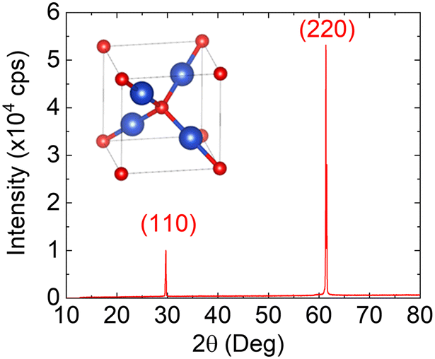 | ||
| Fig. 2 XRD of the Cu2O crystal obtained from Cu under Ar: O2 at 1020 °C showing two narrow, high intensity peaks corresponding to the (110) and (220) crystallographic planes of the cubic crystal of Cu2O; inset shows the cubic unit cell of Cu2O, Cu in blue and O in red. | ||
The structural properties of the Cu2O obtained from 20 μm thick Cu that was pre-annealed under Ar and H2 at 1000 °C and 10 mbar were also investigated by SEM, TEM and HRTEM. A typical SEM image of the Cu2O is shown in Fig. 3(a) and (b). A bright field TEM image is shown in Fig. 3(d) and (e) from which one may observe that the Cu2O surface is covered by a thin layer of CuO consisting of nanocrystals with an average size of ∼10 nm. The surface roughness of the Cu2O is estimated to be about 3 nm. A HRTEM image of the Cu2O/CuO interface is shown in Fig. 4(a). The {10−1}, and {110} lattice fringes of the nanocrystals correspond to the monoclinic structure CuO whose unit cell is shown in Fig. 3(c) while the FFT pattern of the Cu2O square region shown in Fig. 4(a) confirms the cubic crystal structure of Cu2O; the frequencies correspond to the (11−1), (−110) and (02−1) atomic planes of Cu2O phase. More importantly, the high crystal quality of the bulk Cu2O was confirmed by HRTEM as shown in Fig. 4(b).
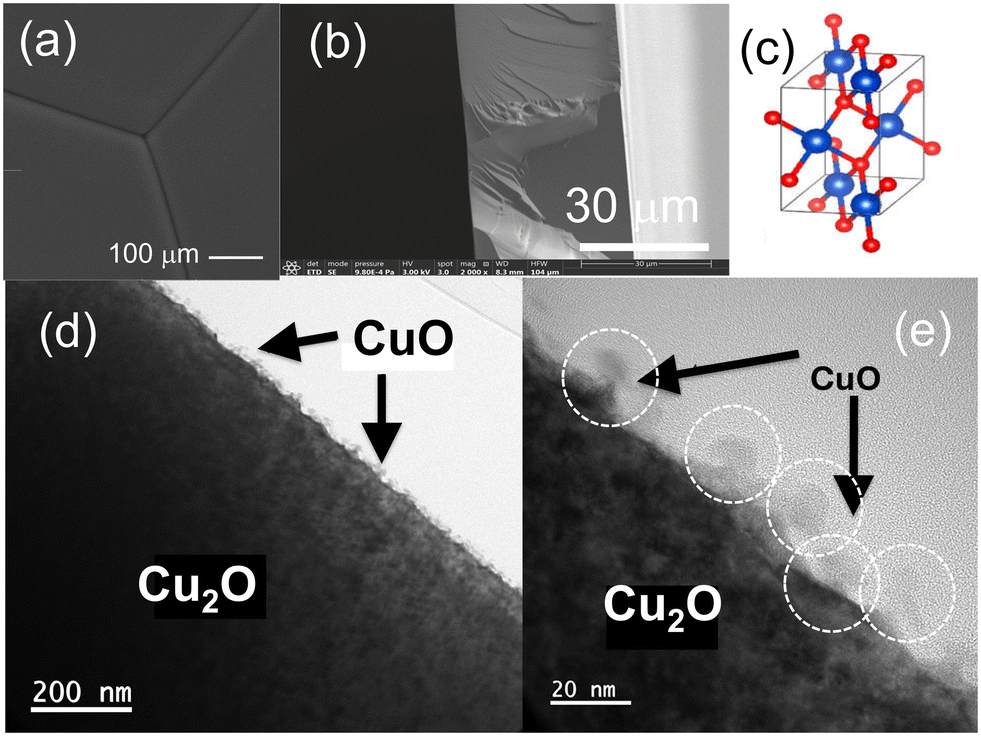 | ||
| Fig. 3 (a) and (b) SEM image of the surface and section of the 30 μm thick Cu2O obtained from Cu under Ar and O2 at 1020 °C (c) unit cell of CuO (d) low magnification, bright field TEM image of the Cu2O showing CuO nanocrystals on the surface of Cu2O (e) higher magnification TEM image of the Cu2O indicating a surface roughness of ∼3 nm. | ||
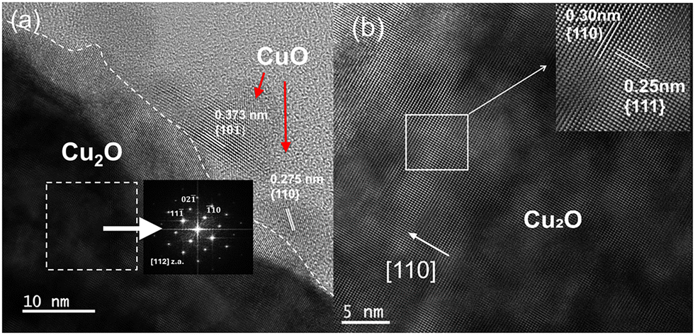 | ||
| Fig. 4 (a) High resolution TEM image of the Cu2O/CuO interface showing the (110) and (10−1) crystallographic planes of the CuO nanocrystals on the surface of Cu2O; inset shows the FFT of the Cu2O square region (b) HRTEM of Cu2O showing the [110] direction; inset shows the {110} and {111} crystallographic planes of the bulk Cu2O. | ||
While we did not observe any bulk inclusions of CuO in the Cu2O by TEM and HRTEM we expect traces of CuO to exist at grain boundaries or as inclusions elsewhere in the Cu2O and further investigations are required to quantify the phase purity of the Cu2O that can be improved greatly by pre-annealing the Cu under H2 as discussed above.
In the past the growth of Cu2O via the thermal oxidation of Cu at elevated temperatures has always been carried out in air that contains O2 as well as H2O but the level of humidity or its effect on the growth of Cu2O was not considered.20–26 In fact, no one has investigated the dry or wet oxidation of Cu above 1000 °C. It is known that the addition of traces of H2O may promote grain growth in accordance with the findings of Liu et al.17 who investigated how the humidity influences the properties of Cu2O obtained at low temperatures. One might argue then that the thermal oxidation of Cu under Ar and O2 at 1020 °C and the growth of high crystal quality Cu2O described here is related to H2O obtained via the reaction of traces of H2 with O2. To clarify this, we investigated the thermal oxidation of Cu under Ar and O2 at 1040 °C and 1 mbar without using H2 and find that Cu2O may be obtained by dry oxidation, see ESI† S2 but its crystal quality and purity are not comparable to that obtained by annealing the Cu under H2. On the other hand, we find that Cu2O cannot be obtained by wet oxidation of Cu at 1040 °C as described in ESI† S3. An excess of H2O alone resulted in the full oxidation of Cu into CuO. It has been shown that the wet oxidation of Cu at low and intermediate temperatures is faster compared to dry oxidation and follows a parabolic law, so it is difficult to control the rate of oxidation especially at very high temperatures. In short, high crystal quality Cu2O can be obtained in a controllable fashion by dry oxidation and the reaction of Cu with O2 but not using only H2O.
We suggest that the high crystal quality Cu2O is obtained due to the strain-energy-driven grain growth in accordance with Xiao et al.26 The oxidation of Cu with O2 initially proceeds with the formation of small nucleation centers of Cu2O on the surface of Cu after which growth occurs as the oxidation front moves inwards via the diffusion of oxygen. The lattice constant of Cu2O is a = 4.2696 Å and that of Cu is 3.615 Å. This difference in the lattice constants leads to the generation of compressive growth strains. According to Xiao et al.26 Cu2O grains undergo rapid diffusion and move preferentially in the vertical growth direction to release the strain through the generation of Frank partial dislocations which grow by absorbing VCu and penetrate through the bulk. The Frank partial dislocations tend to slip along the lattice plane with the densest atoms and the crystal rotates on the sliding surface, triggering grains to orient in a specific direction. Xiao et al.26 showed that (111)-oriented Cu2O with small grains are obtained by surface energy-dominated growth while the (110) oriented Cu2O is obtained by strain-energy-driven grain growth. The Cu2O crystals obtained in this work consist of (110) and (220) high index grains like those of Xiao et al.26 but we did not impose a strain on the Cu. We suggest that the strain-energy-driven grain growth occurs in the Cu2O obtained here probably due to the incorporation of H2 which moves easily and segregates at grain boundaries, voids etc. resulting in strain.
The optical properties of the Cu2O were investigated by steady state photoluminescence (PL) spectroscopy. A typical image of the Cu2O crystal used in this case is shown in Fig. 5(a). The Cu2O exhibited strong PL at 6 K as shown in Fig. 5(b) from which one may observe a peak at 2.01 eV and a side peak at 2.04 eV. A smaller, weak but discernible peak exists at 1.95 eV. To obtain a better understanding of the optical properties it is useful to consider the conduction and valence band potential profile of Cu2O in Fig. 6(a) showing the surface depletion and downward band bending which is usually attributed to the occurrence of oxygen vacancy (VO) donor-like states that are positively charged. It has been suggested that the Femi level (EF) of Cu2O is actually pinned at these surface states related to VO which reside energetically in the upper half of the band gap ∼0.4 eV below the conduction band minimum. In thermodynamic equilibrium, the Fermi level will be constant throughout the p-Cu2O. The boundary conditions i.e., energetic position of the Fermi level with respect to the conduction band edge at the surface and in the bulk govern the overall band bending and extent of depletion. Excitation with photons having energies greater than the gap will lead to the generation of an excess density of electrons and holes. The photogenerated electrons in the surface depletion will move towards the surface and holes will move in the opposite direction into the bulk Cu2O. This will reduce the electric field in the surface depletion until a dynamic equilibrium is reached after which the quasi-Fermi levels will not change with time. However, photoexcited electrons and holes that are generated in the near surface region may recombine via surface states related to crystallographic imperfections. In the past PL has been observed at energies lower than the energy band gap of Cu2O, specifically at 1.47 eV, 1.72 eV, and 1.82 eV which are related to recombination of excitons bound to single charged copper vacancies VCu1+, single charged oxygen vacancies VO1+ and double charged oxygen vacancies VO2+, at temperatures as low as 14 K as depicted schematically in Fig. 5(c).30–32 We do not observe any PL at these energies consistent with a high crystal quality. It should be noted that photogenerated carriers will recombine in a non-radiative fashion in any CuO that exists at the surface or in the bulk so its effect would be to reduce the overall PL intensity. CuO is an indirect energy gap p-type semiconductor with a band gap of ∼1 eV. The CuO/Cu2O heterojunction has a straddled i.e. type I, band line-up and conduction band discontinuity ΔEC(Cu2O/CuO) ∼ 1.0 eV as shown in Fig. 6(b). In this case electrons and holes will be generated in the near surface region upon photoexcitation and recombine inside the CuO which acts as a sink for the photogenerated carriers. The lattice constant of Cu2O is a = 4.2696 Å and CuO has a monoclinic crystal structure with lattice constants of a = 4.6837 and b = 3.4226 Å so this difference in lattice constant will lead to the formation of many crystallographic imperfections at the CuO/Cu2O. The poor properties of the CuO/Cu2O interface are well known so eliminating and preventing the formation of CuO in Cu2O is essential in order to obtain good electrical and optical properties. As we have shown, this was possible by using H2.
 | ||
| Fig. 5 (a) A typical image of the Cu2O obtained after polishing for PL (b) PL spectrum of the 30 μm Cu2O at 6 K showing a large peak at 2.01 eV and side peak at 2.04 eV; a much smaller side peak exists at 1.95 eV (c) schematic energy band diagram showing the generation of photo excited electrons and hole as well as the direct gap radiative recombination and that occurring via donor like states close to the conduction band. | ||
 | ||
| Fig. 6 (a) Conduction and valence band potential profile of Cu2O showing the surface depletion, downward band-bending, work function ϕ and electron affinity χ as well as the energetic position of donor like surface states (b) corresponding band profile of the Cu2O/CuO junction, showing the conduction and valence band offsets as well as states related to crystallographic imperfections at the interface. | ||
The PL observed at 2.01 eV in Fig. 5 is related to band edge transitions in the Cu2O in very good agreement with calculations of the electronic band structure of Cu2O shown in Fig. 7(a) from which we obtained a fundamental, direct energy band gap of 1.96 eV. The first-principles calculations were performed employing Quantum Espresso ab initio code.33,34 In the self-consistent calculations, an energy cutoff for the plane-wave basis of 350 Ryd was used, while an 8 × 8 × 8 Monkhorst–Pack mesh was assumed for the k-space sampling. The structure was geometrically optimized using the PBE exchange–correlation functional35 and the obtained lattice constant, 4.291 Å, is very close to the experimental. Due to the known problem of GGA functionals, like PBE, in reproducing the electronic properties, we employed DFT+U (PBE + U) approximation.36 For the Hubbard parameters, we adopted the values of 11 and 7 eV for Cu-d and O-p orbitals. The combination of these values with the PBE optimized geometry are reported to be accurate for the band gap of Cu2O.37 In Fig. 7(a), we show the obtained band structure of Cu2O, while in (b) the corresponding density of states (DOS) is included. It is worth mentioning that optimizing the structure with PBE + U (instead of plain PBE) leads to an overestimation of the lattice constant (4.475 Å) and to a significant reduction of the band gap (1.71 eV). In Fig. 7(c), we include the DOS obtained by PBE + U for this lattice parameter, and for comparison we also include the DOS obtained by HSE06 (ref. 38) range-separated hybrid-functional.
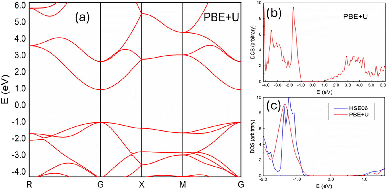 | ||
| Fig. 7 (a) Electronic band structure of Cu2O obtained by PBE + U approximation (for PBE optimized structure) showing that the direct gap is 1.96 eV at the Γ symmetry point, (b) the corresponding DOS, and (c) the DOS with PBE + U compared with that of HSE06, for the PBE + U optimized structure. | ||
Finally, we measured the carrier density and mobility of three different 10 mm × 10 mm Cu2O crystals with a thickness of ∼30 μm after removing the CuO layer on the front and back of the Cu2O in HCl (aq) and HNO3 (aq) to allow forming Ag ohmic contacts. We find that all of the Cu2O crystals are p-type. The largest mobility was found to be μp = 82 cm2 V−1 s−1 at room temperature with a corresponding carrier density of 7.3 × 10 11 cm−3. The other two Cu2O crystals had lower mobilities of μp = 69 cm2 V−1 s−1 and μp = 61 cm2 V−1 s−1 at room temperature with corresponding carrier densities of 8.1 × 1011 cm−3 and 8.8 × 1011 cm−3. These mobilities are smaller than 100 cm2 V−1 s−1 measured by Xiao et al.26 We suggest that the mobility is limited primarily by grain boundary and defect scattering. The hole mobility can be improved by annealing at even higher temperatures leading to the formation of larger grains and eventually a single crystal of Cu2O.
We ought to mention here that the bare surface of Cu2O will be oxidized into CuO upon exposure to ambient conditions over time so we suggest that it is important to remove the CuO on the front and back surface once and for all after which the Cu2O surface has to be passivated immediately with a thin layer of MgO that has a lattice constant of 4.21 Å which is very close to that of Cu2O i.e. 4.2696 Å. The lattice mismatch between MgO and Cu2O is ∼1%. MgO is a transparent, insulator with a large energy band gap thereby allowing light to reach the underlying Cu2O. We also have to mention that the Cu2O crystals obtained by thermal oxidation of Cu foils are brittle and bent. One may obtain circular like, flat wafers by sawing boules of Cu2O grown by the floating zone method but this takes a significantly longer time and is much more energy consuming. The growth of high quality, polycrystalline and even single crystal Cu2O from Cu foils with a thickness of 10–50 μm's is attractive due to the shorter times required for complete oxidation and crystallization by annealing.
It is necessary then to obtain flat Cu2O crystals from Cu foils with a thickness of a few tens of μm's which may be achieved by controlling the thermal oxidation, heating and cooling rates. These issues must be resolved before moving into the fabrication of devices such as p–n heterojunction solar cells as well as cavities for the observation of exciton-polaritons.
4. Conclusions
We have carried out a detailed investigation into the thermal oxidation of Cu at elevated temperatures between 1020 °C and 1040 °C under Ar and O2. Care was taken to eliminate oxides and promote grain growth in the Cu by annealing under Ar: H2 prior to oxidation. We obtain ruby red Cu2O crystals that consist of ∼500 μm2 grains with a cubic crystal structure. In addition, we show that high crystal quality and phase purity Cu2O is obtained by dry not wet oxidation. The crystal quality and phase purity of the Cu2O was improved significantly by pre-annealing the Cu under Ar: H2 at 1020 °C and 10 mbar for up to 3 hours. The Cu2O obtained in this way exhibited clean PL at 6.5 K with a maximum at 2.01 eV corresponding to the direct energy gap in very good agreement with calculations of the electronic band structure. We did not observe any emission related to crystallographic imperfections confirming the high crystal quality and phase purity of the Cu2O. The Cu2O crystals obtained in this way were p-type and exhibited mobilities between μp = 61 and 82 cm2 Vs−1 which may be improved by annealing at higher temperatures for longer times.Data availability
The data supporting this article has been included as part of the ESI.†Author contributions
M. Zervos was responsible for the growth of the Cu2O crystals, X-ray diffraction, microscopy, hall effect and writing up; I. Paschos and P. Savvidis were responsible for the measuring the optical properties and writing up; N. Florini, K. Koutsokostas and P. Komninou were responsible for the TEM/HRTEM and writing up; N. N. Lathiotakis, P. M. Levendis and S. Marinakis were responsible for the electronic band structure theoretical calculations and writing up.Conflicts of interest
There are no conflicts of interest to declare.Acknowledgements
The first author acknowledges Prof. E. Leontidis, Department of Chemistry at the University of Cyprus for many useful discussions concerning the growth of the Cu2O.References
- C. Malerba, F. Biccari, C. L. A. Ricardo, M. D'Incau, P. Scardi and A. Mittiga, Absorption Coefficient of Bulk and Thin Film Cu2O, Sol. Energy Mater. Sol. Cells, 2011, 95, 2848–2854 CrossRef CAS.
- K. K. Markose, M. Shaji, S. Bhatia, P. R. Nair, K. J. Saji, A. Antony and A. M. K. Jayaraj, Novel Boron-Doped p-Type Cu2O Thin Films as a Hole-Selective Contact in c-Si Solar Cells, ACS Appl. Mater. Interfaces, 2020, 12, 12972–12981 CrossRef CAS PubMed.
- Y. Liu, J. Zhu, L. Cai, Z. Yao, C. Duan, Z. Zhao, C. Zhao and W. Mai, Solution-Processed High-Quality Cu2O Thin Films as Hole Transport Layers for Pushing the Conversion Efficiency Limit of Cu2O/Si Heterojunction Solar Cells, Sol. RRL, 2020, 4, 1900339 CrossRef CAS.
- S. Shibasaki, Y. Honishi, N. Nakagawa, M. Yamazaki, Y. Mizuno, Y. Nishida, K. Sugimoto and K. Yamamoto, Highly Transparent Cu2O Absorbing Layer for Thin Film Solar Cells, Appl. Phys. Lett., 2021, 119, 242102 CrossRef CAS.
- A. Lakshmanan, Z. C. Alex and S. R. Meher, Recent Advances in Cuprous Oxide Thin Film-Based Photovoltaics, Mater. Today Sustain., 2022, 20, 100244 Search PubMed.
- X. Liu, J. Chen, P. Liu, H. Zhang, T. An and H. Zhao, Controlled Growth of CuO/Cu2O Hollow Microsphere Composites as Efficient Visible-Light-Active Photocatalysts, Appl. Catal., A, 2016, 521, 34–41 CrossRef CAS.
- B. Koiki and O. A. Arotiba, Cu2O as an Emerging Semiconductor in Photocatalytic and Photo Electrocatalytic Treatment of Water Contaminated with Organic Substances: A Review, RSC Adv., 2020, 10, 36514–36525 RSC.
- Y. H. Zhang, M. M. Liu, J. L. Chen, S. M. Fang and P. P. Zhou, Recent Advances in Cu2O-Based Composites for Photocatalysis: A Review, Dalton Trans., 2021, 50, 4091–4111 RSC.
- G. Liu, F. Zheng, J. Li, G. Zeng, Y. Ye, D. M. Larson, J. Yano, E. J. Crumlin, J. W. Ager, L. Wang and F. M. Toma, Investigation and Mitigation of Degradation Mechanisms in Cu2O Photoelectrodes for CO2 Reduction to Ethylene, Nat. Energy, 2021, 6, 1124–1132 CrossRef CAS.
- E. F. Gross, Optical Spectrum of Excitons in the Crystal Lattice, Il Nuovo Cim., 1956, 3, 672–701 CrossRef CAS.
- T. Kazimierczuk, D. Fröhlich, S. Scheel, H. Stolz and M. Bayer, Giant Rydberg excitons in the Copper Oxide Cu2O, Nature, 2014, 514, 343–347 CrossRef CAS PubMed.
- K. Orfanakis, S. K. Rajendran, V. Walther, T. Volz, T. Pohl and H. Ohadi, Rydberg Exciton–Polaritons in a Cu2O Microcavity, Nat. Mater., 2022, 21, 767–772 CrossRef CAS PubMed.
- K. Kawaguchi, R. Kita, M. Nishiyama and T. Morishita, Molecular Beam Epitaxy Growth of CuO and Cu2O Films with Controlling the Oxygen Content by the Flux Ratio of Cu/O+, J. Cryst. Growth, 1994, 143, 221–226 CrossRef CAS.
- T. Iivonen, M. J. Heikkilä, G. Popov, H. E. Nieminen, M. Kaipio, M. Kemell, M. Mattinen, K. Meinander, K. Mizohata, J. Räisänen, M. Ritala and M. Leskelä, Atomic Layer Deposition of Photoconductive Cu2O Thin Films, ACS Omega, 2019, 4, 11205–11214 CrossRef CAS PubMed.
- S. F. U. Farid, D. Cherns, J. A. Smith, N. A. Fox and D. J. Fermín, Pulsed Laser Deposition of Single-Phase n- and p-type Cu2O Thin Films with Low Resistivity, Mater. Des., 2020, 193, 108848 CrossRef.
- A. S. Rahman, M. A. Islam and K. M. Shorowordi, Electrodeposition and Characterization of Copper Oxide Thin Films for Solar Cell Applications, Procedia Eng., 2015, 105, 679–685 CrossRef CAS.
- H. Liu, V. H. Nguyen, H. Roussel, I. Gélard, L. Rapenne, J. L. Deschanvres, C. Jiménez and D. Muñoz-Rojas, The Role of Humidity in Tuning the Texture and Electrical Properties of Cu2O Thin Films Deposited via Aerosol-Assisted CVD, Adv. Mater. Interfaces, 2018, 6, 1801364 CrossRef.
- S. Chatterjee and A. J. Pal, Introducing Cu2O Thin Films as a Hole-Transport Layer in Efficient Planar Perovskite Solar Cell Structures, J. Phys. Chem. C, 2016, 120, 1428–1437 CrossRef CAS.
- S. Shibasaki, Y. Honishi, N. Nakagawa, M. Yamazaki, Y. Mizuno, Y. Nishida, K. Sugimoto and K. Yamamoto, Highly Transparent Cu2O Absorbing Layer for Thin Film Solar Cells, Appl. Phys. Lett., 2021, 119, 242102 CrossRef CAS.
- R. S. Toth, R. Kilkson and D. Trivich, Preparation of Large Area Single-Crystal Cuprous Oxide, J. Appl. Phys., 1960, 31, 1117–1121 CrossRef CAS.
- S. Mrowec and A. Stokłosa, Oxid. Met., 1971, 3, 291–311 CrossRef CAS.
- W. S. Brower Jr and H. S. Parker, Growth of Single Crystal Cuprous Oxide, J. Cryst. Growth, 1971, 8, 227–229 CrossRef.
- R. D. Schmidt-Whitley, M. Martinez-Clemente and A. Revcolevschi, Growth and Microstructural Control of Single Crystal Cuprous Oxide Cu2O, J. Cryst. Growth, 1974, 23, 113–120 CrossRef CAS.
- S. Mani, J. I. Jang, J. B. Ketterson and H. Y. Park, High-Quality Cu2O crystals with Various Morphologies Grown by Thermal Oxidation, J. Cryst. Growth, 2009, 311, 3549–3552 CrossRef CAS.
- S. A. Lynch, C. Hodges, S. Mandal, W. Langbein, R. P. Singh, L. A. P. Gallagher, J. D. Pritchett, D. Pizzey, J. P. Rogers, C. S. Adams and M. P. A. Jones, Rydberg Excitons in Synthetic Cuprous Oxide (Cu2O), Phys. Rev. Mater., 2021, 5, 084602 CrossRef CAS.
- M. Xiao, P. Gui, K. Dong, L. Xiong, J. Liang, F. Yao, W. Li, Y. Liu, J. Li, W. Ke, C. Tao and G. Fang, Quasi-Single Crystalline Cuprous Oxide Wafers via Stress-Assisted Thermal Oxidation for Optoelectronic Devices, Adv. Funct. Mater., 2022, 32, 2110505 CrossRef CAS.
- M. Wu, Z. Zhang, X. Xu, Z. Zhang, Y. Duan, J. Dong, R. Qiao, S. You, L. Wang, J. Qi, D. Zou, N. Shang, Y. Yang, H. Li, L. Zhu, J. Sun, H. Yu, P. Gao, X. Bai, Y. Jiang, Z. Wang, F. Ding, D. Yu, E. Wang and K. Liu, Seeded Growth of Large Single-Crystal Copper Foils with High-Index Facets, Nature, 2020, 581, 406–410 CrossRef CAS PubMed.
- K. Y. Maimaiti, M. Nolan and S. D. Elliott, Reduction Mechanisms of the CuO (111) Surface Through Surface Oxygen Vacancy Formation and Hydrogen Adsorption, Phys. Chem. Chem. Phys., 2014, 16, 3036–3046 RSC.
- S. Jin, M. Huang, Y. Kwon, L. Zhang, B. W. Li, S. Oh, J. Dong, D. Luo, M. Biswal, B. V. Cunning, P. Bakharev, I. Moon, W. J. Yoo, D. C. Camacho-Mojica, Y. J. Kim, S. H. Lee, B. Wang, W. K. Seong, M. Saxena, F. Ding, H. J. Shin and R. Ruoff, Colossal Grain Growth Yields Single-Crystal Metal Foils by Contact-Free Annealing, Science, 2018, 362, 1021–1025 CrossRef CAS PubMed.
- C. K. Teh and F. L. Weichman, Photoluminescence and Optical Absorption Studies of the Effects of Heat Treatment on Cuprous Oxide, Can. J. Phys., 1983, 61, 1423–1427 CrossRef CAS.
- H. Solache-Carranco, G. Juárez-Díaz, A. Esparza-García, M. Briseño-García, M. Galván-Arellano, J. Martínez-Juárez, G. Romero-Paredes and R. Peña-Sierra, Photoluminescence and X-ray Diffraction Studies on Cu2O, J. Lumin., 2009, 129, 1483–1487 CrossRef CAS.
- T. Ito and T. Masumi, Detailed Examination of Relaxation Processes of Excitons in Photoluminescence Spectra of Cu2O, J. Phys. Soc. Jpn., 1997, 66, 2185–2193 CrossRef CAS.
- P. Giannozzi, S. Baroni, N. Bonini, M. Calandra and R. Car, et al. Quantum Espresso: a Modular and Open-Source Software Project for Quantum Simulations of Materials, J. Phys.:Condens. Matter, 2009, 21, 395502 CrossRef PubMed.
- P. Giannozzi, O. Andreussi, T. Brumme, O. Bunau and M. B. Nardelli, et al. Advanced Capabilities for Materials Modelling with Quantum ESPRESSO, J. Phys.:Condens. Matter, 2017, 29, 465901 CrossRef CAS PubMed.
- J. P. Perdew, K. Burke and M. Ernzerhof, Generalized Gradient Approximation Made Simple, Phys. Rev. Lett., 1996, 77, 3865 CrossRef CAS PubMed.
- V. I. Anisimov, J. Zaanen and O. K. Andersen, Band Theory and Mott Insulators: Hubbard U Instead of Stoner I, Phys. Rev. B: Condens. Matter Mater. Phys., 1991, 44, 943 CrossRef CAS PubMed.
- E. R. A. Beronio, I. R. Colambo and A. A. B. Padama, The Effects of Substitutional Doping on Cu Vacancy Formation in Cu2O(111): a Density Functional Theory Study, Phys. Chem. Chem. Phys., 2021, 23, 8800 RSC.
- J. Heyd, G. E. Scuseria and M. Ernzerhof, Hybrid Functionals Based on a Screened Coulomb Potential, J. Chem. Phys., 2003, 118, 8207 CrossRef CAS.
Footnote |
| † Electronic supplementary information (ESI) available. See DOI: https://doi.org/10.1039/d4ce01276c |
| This journal is © The Royal Society of Chemistry 2025 |