
 Open Access Article
 This Open Access Article is licensed under a
 Creative Commons Attribution 3.0 Unported Licence
Building blocks for nanophotonic devices and metamaterials
Natalie
Shultz
a and
Euan
McLeod
 *ab
*ab
aWyant College of Optical Sciences, University of Arizona, 1630 E University Blvd, Tucson, AZ, USA. E-mail: euanmc@optics.arizona.edu
bBIO5 Institute, University of Arizona, 1657 E Helen St, Tucson, AZ, USA
First published on 24th January 2025
Abstract
Nanophotonic devices control and manipulate light at the nanometer scale. Applications include biological imaging, integrated photonic circuits, and metamaterials. The design of these devices requires the accurate modeling of light–matter interactions at the nanoscale and the optimization of multiple design parameters, both of which can be computationally demanding and time intensive. Further, fabrication of these devices demands a high level of accuracy, resolution, and throughput while ideally being able to incorporate multiple materials in complex geometries. To address these considerations in the realization of nanophotonic devices, recent work within our lab has pursued the efficient and accurate modeling of nanoparticles and the assembly of complex 3D micro- and nanostructures using optical tweezers. This Feature Article review highlights these developments as well as related efforts by others in computation and fabrication methods related to nanophotonic devices and metamaterials.
1 Introduction
Nanophotonic devices1 enable the control of light at the nanoscale. This capability is important for the generation, transport and detection of light through the use of devices such as nanolasers,2 waveguides,3 and metasurfaces or metamaterials.4 Operating in the nanoscale allows for miniaturization of components for compact, on-chip systems5 and can lead to novel optical phenomena at operating ranges not seen in other size scales. Materials used for nanophotonic devices can vary from dielectrics6,7 to semiconductors8 to metals9,10 and can also include soft materials such as polymers11 and colloids.12 The nanoscale features in these devices make modeling and fabrication an interesting and sometimes challenging pursuit.Nanophotonic devices can be realized in a variety of ways, including lithography, self-assembly, and directed assembly. For example, some metamaterials use lithographically-defined layers of metal and dielectric materials13–15 to obtain a particular response, while other metamaterials are self-assembled from nanoparticle building blocks.16,17 The versatility in fabrication aspects such as materials and structures makes the development of nanophotonic devices both rich and complex.
The workflow for developing nanophotonic devices is shown in Fig. 1, starting with device design, then modeling, and ending with fabrication. The theme among each of these steps is accuracy and efficiency. The design step often requires optimization of parameters including material, size and position that can have costs in terms of long computational times and large amounts of memory. The modeling of materials ranging from dielectrics to metals on the nanoscale is vital for understanding interactions within and outside a device, although this modeling often has similar drawbacks related to time and resources. Fabrication demands a high level of resolution that ideally is able to incorporate a variety of materials over large scales quickly and at low cost.
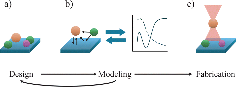 | ||
| Fig. 1 Example of nanophotonic device workflow. (a) Design may begin with an initial set of parameters, such as nanoparticle locations, sizes, and materials. (b) Modeling explains interactions among device building blocks, as well as between the building blocks and surrounding structures. Iterations between design and modeling are often necessary to achieve the intended device response. (c) Fabrication can be achieved through various techniques. In our lab, a central approach is based on optical tweezers. The efficiency and accuracy of each of these steps is important in the creation of functional devices. | ||
Unlike a typical review article, the purpose of this Feature Article is to provide the scientific community with information and perspectives on areas within nanophotonic design and fabrication, while emphasizing the contributions of our lab to this field. This article differs from previous review articles from our own and other labs due to this specific focus on how we aim to design and assemble nanophotonic materials and devices.
Work within our lab has contributed to improving the accuracy and efficiency of each of the previously mentioned workflow stages. Efforts related to design have incorporated the effects of a substrate, which is an important consideration in moving towards physically realizable devices, especially for applications like metasurfaces. The effects of the skin depth on the interaction of light with metallic nanoparticles has been clarified, leading to more accurate modeling of optical trapping forces on these particles. We have shown how to modify the angular spectrum method of propagation to better account for light-nanoparticle interactions in lensfree digital holography. These works leverage approximations and methods to speed up computational times and decrease strain on computing resources while being compared to the gold standard to ensure a high level of accuracy. To address fabrication of nanophotonic devices, our lab uses optical tweezers to assemble microstructures composed of nano- and microparticle building blocks. This work is unique regarding the scale of structures that have been constructed, including the largest structure assembled using optical tweezers, and offers advantages compared to other microfabrication processes when considering the achievable complexity of structures and ability to use particles of varying size and material in assembly. We have demonstrated the fastest optical manipulation of nanoparticles, which relates to fabrication throughput. Further, this setup can augment existing devices, which increases the potential applications and implementation of assembled structures. These efforts offer the community multiple tools for the accurate and efficient design, modeling, and fabrication of nanophotonic devices.
This Feature Article is organized into three main sections: modeling and design, fabrication, and interesting concepts and applications. The beginning of each section provides a summary of relevant work that has been conducted within our lab while the remainder of the section relates it to other work in the community. While major topics and techniques are included to provide insight across a broad scope, this is not meant as a comprehensive review of any one specific area. The specific examples provided in the final section are meant to present work that is expected to contribute to future advancements, but is by no means exhaustive in value or ingenuity.
2 Modeling and design
The computation and modeling of nanophotonic interactions, i.e., how light interacts with nanoscale objects, is important for validating device designs before experimental prototyping. As will be addressed in the following section, obtaining results with high accuracy often comes at the cost of long computational time and large amounts of memory required. In this way, approximations or computational methods that can reduce the computational cost while remaining comparatively accurate are valuable and necessary for future innovation.2.1 Skin depth correction
Rayleigh scattering is a useful approximation for calculating light scattering when the particle size is much smaller than the wavelength of light. This calculation approximates the particle as a dipole whose strength is proportional to the particle polarizability. The Clausius–Mossotti (CM) relation approximates the polarizability for dielectric and metallic particles and incorporates the particle volume. An effective volume correction was proposed in 1994 to account for the material skin depth,18 which is related to the imaginary part of the refractive index.19 For metallic particles, the skin depth effect results in a shell of interaction volume close to the particle surface; however, experimental data that spanned decades concerning trapping forces have not shown substantial support for correcting the volume based on the size of this shell. By comparing scattering and optical force calculations, we have shown that the complex permittivity applied to the full volume more accurately accounts for the skin-depth effect than any volume correction.19This work first compared the accuracy of four different polarizability models with far-field scattering from a plane wave to Mie theory and finite-difference time-domain (FDTD) simulations. Although the polarizability models that include an effective volume correction do not perform as well as the other dipole models at both 1064 nm and 550 nm for forward and backward scattering, FDTD simulations of a 30 nm and 300 nm diameter gold sphere confirm that the skin depth is a real phenomenon. This is further seen by comparing a solid gold nanosphere and a hollow gold nanoshell with an inner radius chosen such that the total volume is equivalent to the effective volume of a solid nanosphere with the same outer radius. Although there is some difference between the far-field diffraction results using FDTD for the solid and hollow nanosphere, this disparity stems from optical differences while the overall agreement between the two supports the skin depth effect such that the core of the particle does not significantly contribute to scattered field. The models with an effective volume also are not accurate for either the solid or hollow nanosphere.19
To investigate optical force calculations, the time-averaged optical force calculated using the dipole approximation was compared to computations involving Maxwell's stress tensor.19 For 1064 nm excitation, the dipole models without an effective volume are most accurate for a particle radius less than 200 nm, while for a particle radius between 200 nm and 400 nm, the model with skin depth correction has the least error, although this is seen as an empirical coincidence, since the dipole models in general are relatively inaccurate at this size range. The percent error for varying particle sizes for this wavelength is shown in Fig. 2. For 550 nm excitation and particle radius less than 50 nm, the dipole models without skin depth correction are again most accurate while all models have significant error for greater radii.19
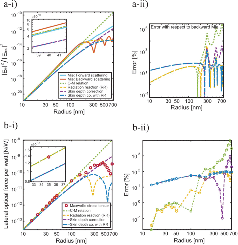 | ||
| Fig. 2 Skin depth correction in dipolar models of nanoparticles illuminated with 1064 nm wavelength light. (a) Far-field scattering calculations. Scattering amplitudes (a-i) and percent errors with respect to Mie backward scattering (a-ii) are shown. (b) Lateral optical forces. Total force (b-i) and error (b-ii) compared to Maxwell's stress tensor calculations are shown. Panel adapted from ref. 19 with permission from American Chemical Society, copyright 2019. | ||
These findings are significant for scattering and optical force calculations, which are frequently considered in nanophotonic modeling and applications such as optical tweezing and biosensing.
2.2 Angular spectrum method for random nanoparticle arrays
Applications such as lens-free microscopy that rely on image reconstruction commonly use the angular spectrum method (ASM) to backpropagate measurements from the sensor plane to the object plane.20 Although this method is computationally fast, inaccuracies arise when applied to nanoscale objects because only the propagation of light is considered, and not light–matter interaction.20 For example, on the macro scale, when rays of light impinge on an object, they are blocked, attenuated, and/or delayed in phase; however, on the nanoscale, instead of light rays, one must consider the nanoparticles' absorption and scattering cross sections, which differ considerably from their physical size. The angular spectrum method does not inherently consider these optical cross sections. Our work addressed the accuracy of ASM transmission models for scattering of nanoscale objects imaged with digital holography.To determine the accuracy of the ASM models, results were compared to the discrete dipole approximation (DDA), FDTD, and Mie theory. DDA best balances computational time and accuracy. By writing our own DDA code, a sparse array of particles can be handled where the computational time scales with the total number of dipoles involved, as opposed to open-source codes that require a regular gridded spacing of dipoles, resulting in computational time scaling with the total domain size. This in-house code was validated against Mie theory and FDTD.20 While Mie theory works well for scattering from a single particle, it is less valid when increasing the number of particles in an array due to interparticle coupling. Although FDTD can be used for an arbitrary number of particles, due to computational time, it is not practical in all scenarios; Mie theory was thus used to set an error bound when approximating particles as single dipoles and FDTD simulations were executed for instances when there could be large errors in DDA calculations.
Three transmission models were investigated: a dipole-matched transmission (DMT) model, the optical path length (OPL) transmission function, and a binary amplitude mask (BAM) transmission function.20 In the DMT model, the analytical far-field scattering from a single dipolar nanoparticle due to a plane wave is used to establish the amplitude attenuation and phase delay introduced to the field by each particle. For the OPL model, nanoparticles are modeled as small slabs with the attenuation and phase delay of the field resulting from the thickness and index of refraction of the material of the slab. Lastly, the BAM model represents nanoparticles as an opaque mask which can apply to materials with low transmission at visible wavelengths. Polystyrene and gold particles were tested with the DMT and OPL models while the BAM model was only applied to gold particles.
The wavelength used was 610 nm, which is the emission wavelength for europium chelate nanoparticles, and the particle sizes were chosen as 30 nm, 60 nm, and 100 nm. Table 1 summarizes findings from this work, which found that using the ASM, the most accurate transmission model was the DMT which was accurate for all three sizes of high density polystyrene and medium to low densities of gold.20
| Particle size | Polystyrene | Gold | ||||
|---|---|---|---|---|---|---|
| Accurate and fast | Accurate and slow | Inaccurate | Accurate and fast | Accurate and slow | Inaccurate | |
| λ/20 | ASM-DMT | DDA | ASM-DMT | DDA | ASM-DMT | |
| (N1 < 1375) | (N1 ≥ 1375) | |||||
| ASM-OPL | FDTD | FDTD | ASM-OPL | |||
| (N1 ≤ 206) | ||||||
| Mie | Mie | ASM-BAM | ||||
| λ/10 | ASM-DMT | FDTD | ASM-DMT | FDTD | ASM-DMT | |
| (N1 < 229) | (N1 ≥ 229) | |||||
| ASM-OPL | DDA | ASM-OPL | ||||
| DDA | Mie | ASM-BAM | ||||
| Mie | ||||||
| λ/6 | ASM-DMT | FDTD | ASM-DMT | FDTD | ASM-DMT | |
| (N81 < 10) | (N81 ≥ 10) | |||||
| (N1 < 41) | (N1 ≥ 41) | |||||
| ASM-OPL | DDA | ASM-OPL | ||||
| DDA | ASM-BAM | ASM-BAM | ||||
| (N81 > 206) | (N81 ≤ 206) | |||||
| Mie | Mie | |||||
As previously stated, this work is applicable to digital holography and enables fast computations of nanoscale objects including light–matter interaction.
2.3 DDA-with-substrate
The time required to design a metasurface is affected by the number of free parameters to optimize in the design as well as the time it takes to perform forward simulations of a particular candidate design during each iteration. While various optimization methods and tricks exist to reduce the overall computational time—some of which will be mentioned in later sections—the focus of this section is how to reduce the time of individual forward simulations. The DDA can be used to compute scattering and absorption from particles of arbitrary composition and geometry and is less computationally expensive than finite difference methods. Discretizing structures with large volumes into smaller dipoles can satisfy this approximation but can be cumbersome for applications, such as metasurfaces, where particles are near a substrate surface. To retain the efficiency of DDA, substrate effects can be handled analytically, although difficulties related to numerical integration and application of fast Fourier transforms in calculations has limited the use of this technique. We compared the accuracy and efficiency of three DDA methods with four polarizability models, validated against FDTD simulations.21One of the DDA methods that was investigated discretized the substrate while the other two analytically accounted for substrate effects (reflection and transmission) from a dipole source using a 2D Cartesian Green's function or a 1D cylindrical Green's function. The 1D Green's function approach has the fastest computation time of the three DDA methods and is at least an order of magnitude faster than FDTD.21 To assess accuracy of the 1D Green's function method, the Clausius–Mossotti (CM) relation, radiation reaction correction (RR), digitized Green's function (DGF), and lattice dispersion relation (LDR) were the four considered dipole models and for both s- and p-polarizations. Field differences were compared according to pattern error and power error, and it is found that although the CM and RR models have low pattern error, they have relatively greater power error, whereas the DGF model balances these two errors. LDR is not recommended due to a high level of error in both parameters. It is also noted that power error can be corrected by multiplying by a constant factor.
The effects of structure shape and material on DDA performance is also important for many applications. Gold and germanium particles were tested with s- and p-polarization and results indicate that by more finely discretizing the structure, the pattern and power error are reduced with simulation times approximately proportional to the number of dipoles.21 There is a noticeable difference in power error between the two materials; however, pattern errors are less than 1% for both materials, shown in Fig. 3. These results indicate that our DDA-with-substrate method can be applied to both metals and high-index dielectrics. The refractive index of the substrate was similarly tested by using silicon and silica; for both polarizations, the silicon substrate had larger pattern and power errors. In terms of shape dimension, more dipoles in contact with the substrate tends to increase the power error while the pattern error remains similar.21
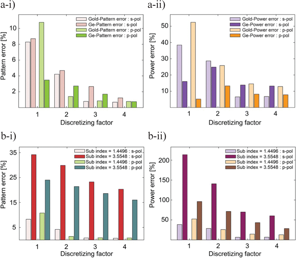 | ||
| Fig. 3 Error in 1D cylindrical Green's function DDA simulations of nanoparticles touching a substrate. The gold standard for comparison is FDTD simulation. (a) Effect of different nanoparticle materials on a silica substrate. Pattern error (a-i) and power error (a-ii) are plotted. (b) Effect of different substrate materials supporting a gold nanoparticle. Pattern error (b-i) and power error (b-ii) are shown. Panel adapted from ref. 21 with permission from De Gruyter, copyright 2023. | ||
Advantages of the 1D cylindrical Green's function include scaling of computational time with the number of particles and monitor sampling points instead of the simulation domain size, accurate simulation of weak coupling and scattering over large areas, and physical understanding of contributions to optical properties. However, downsides to this approach include not being able to handle nonlinear optical properties and isolated rather than periodic domains, though including higher order terms in the dipole moment addresses the former disadvantage and there are ways to approach the latter challenge.21
With metamaterial design for nanophotonic devices becoming increasingly prevalent, this work provides a meaningful tool to increase the accuracy and efficiency of relevant computations.
2.4 Device design in the nanophotonic community
Beyond improving the speed of forward electromagnetic solvers, overall nanophotonic device design can be improved by using efficient design algorithms that minimize the number of iterations required to converge to a satisfactory design. Often, the design approach involves the optimization of system parameters such as the sizes, shapes, materials, and locations of each building block, which could lead to thousands of free parameters. The map shown in Fig. 4a is taken from a relevant and comprehensive review by Ma et al., illustrating the breadth of computational methods and applications for nanophotonic devices.22 Below, we break down these approaches into several categories.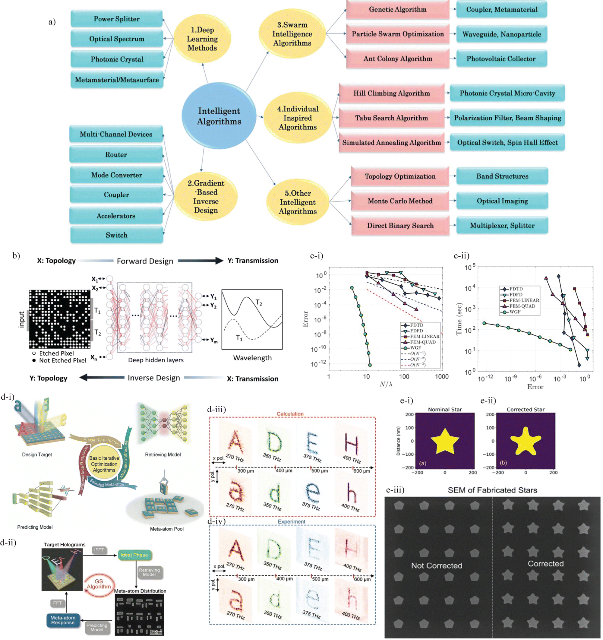 | ||
| Fig. 4 (a) Intelligent nanophotonic design algorithms. Map of various kinds of algorithms and applications. Panel reproduced from ref. 22 with permission from Chinese Optics Letters, copyright 2021. (b) Forward and inverse design using deep neural networks. Panel reproduced from ref. 23 with permission from IEEE, copyright 2021. (c) The boundary integral equation method. Convergence (c-i) and time versus error (c-ii) are compared to standard and commercial or open-source solvers (finite-difference time-domain (FDTD), finite-difference frequency-domain (FDFD), and finite element method using linear (FEM-LINEAR) or quadratic (FEM-QUAD) elements). Dashed lines are first-, second-, and third-order convergence. Panel reproduced from ref. 24 with permission from American Chemical Society, copyright 2019. (d) Multifunctional device design. (d-i) Incorporation of statistical machine learning in retrieving and predicting models. (d-ii) GS algorithm in design flow chart with SEM image of fabricated device for multifunctional metasurface holograms. (d-iii) and (d-iv) Calculated versus experimental results for a device operating with four frequencies and at four positions along the image plane. Panel reproduced from ref. 25 with permission from John Wiley and Sons, copyright 2022. (e) Design process considering fabrication imperfections. (e-i) and (e-ii) Nominal and corrected star patterns. (e-iii) Fabrication results and SEM image of fabricated arrays. Panel reproduced from ref. 26 with permission from American Chemical Society, copyright 2023. | ||
Nanophotonic inverse design has been used in areas ranging from imaging using diffractive elements to free-electron light sources. Work by Bayati et al. applied this approach to the design of an extended depth of focus meta-optic to help overcome challenges related to chromatic aberration in diffractive elements like metalenses; this work produced a high numerical aperture metalens that operates over a large spectral bandwidth and exhibits a symmetric point spread function.35 For Haeusler et al., nanophotonic inverse design was incorporated for work related to Smith–Purcell radiation that is produced by free electrons moving through a grating. Inverse design was used to design the grating and resulted in a three times higher efficiency and more than two times higher power than previous work.36
Nanophotonic inverse design is commonly implemented using the adjoint method, as was done for the previously mentioned work by Bayati et al. The adjoint method allows for efficient computation of the gradient of an objective function,34,37,38 which is valuable for reducing overall computational time. Another example of this implementation involves the design of digital nanophotonic devices, including a power divider and dual-mode demultiplexer.39 The reported design process is carried out in three steps, where the adjoint method is used in the first two steps and brute-force optimization is used in the final step. This hybrid method is expected to increase efficiency by five times.39 The adjoint method for inverse design has also been applied to nonlinear devices. For example, nonlinearity can be accounted for and directly included in the gradient calculation to be applied to Kerr nonlinearity for optical switches.34 This extension to nonlinear device design is valuable to expand the range of application, even with the potential to be generalized to include other nonlinear phenomena.
These advantages are also capitalized upon by Ma et al. in the development of multifunctional metasurfaces using statistical machine learning.25 Statistical machine learning connects physical parameters of the individual components of the metasurface to its response and establishes retrieving and predicting models, as illustrated in Fig. 4d. The retrieving model produces potential meta-atoms and the predicting model determines their performance; these models are embedded in an optimization algorithm that is application-specific and chosen by the user.25 The design process for a dual-polarization metasurface hologram that operates at up to four frequencies is given in Fig. 4d. Here the Gerchberg–Saxton (GS) algorithm is used and the experimental verification of these designs, also shown in Fig. 4d for the four-frequency device, highlights the ability of machine learning to successfully produce non-intuitive designs.
Other work incorporating deep learning has been applied to the design of power splitters.23 This work showed how three models can be implemented: a forward model, an inverse model, and a generative model that uses both forward and inverse aspects. This work showed how deep neural networks can be beneficial for predicting an optical response or design topology, and generating new designs. Deep learning has also been leveraged to aid in finite difference frequency domain simulations involved in inverse design problems.48 This application of deep learning is used to predict the field distribution and notably decreases simulation time and resources by decreasing the required number of iterations for the design process by 53%. Further, deep learning is able to capture complex interactions in nanophotonic systems that are significant, especially when considering nonlinear effects and applying inverse design.49
As these few examples demonstrate, AI is expected to contribute significantly to the development of more advanced and novel nanophotonic designs. However, some challenges with AI remain. With any implementation of machine learning, a large set of data is typically required for training and verification purposes, which does not completely alleviate computationally expensive simulations. Tools like data augmentation, transfer learning, unsupervised learning, and using pre-trained models can in general aid in this issue while in the context of photonic devices, adaptive wavelength sampling can help address this concern.50 Another recent study applied the Taguchi method to reduce simulation requirements while important information contained in design variation is retained.49 Something else to consider in machine learning methods is the concept of overfitting. A hybrid approach using supervised and unsupervised learning and preprocessing that relies upon clustering algorithms and an encoder model was shown to reduce the mean squared error by more than 51% compared to a more traditional way of training artificial neural networks.51 Another hybrid approach that uses supervised learning and reinforcement learning was shown to reduce dependence on training data and allow for model predictions that are more general.52 No doubt such efforts will continue to develop and evolve to minimize such drawbacks and maximize the favorable aspects of this approach.
3 Fabrication
Nanophotonic device fabrication can be challenging due to the required small feature sizes. A multitude of methods have been developed to achieve high resolution through different techniques and with varying levels of complexity. This section begins with an overview of the Optical Positioning and Linking (OPAL) platform in our lab that is used for micro- and nano-fabrication. Following this is a discussion of how OPAL fits among alternative established nanofabrication techniques separated between top-down and bottom-up methods.3.1 Optical positioning and linking (OPAL) platform
Optical tweezing allows for the manipulation of objects from the atomic to micro-scale and was first proposed by Arthur Ashkin in 1969.54 When light is scattered by a particle, the momentum of the light is redirected. This change in momentum necessitates a corresponding force on the particle according to Newton's second law. This force can be decomposed into two components: gradient and scattering forces. The gradient force is proportional to the gradient of the light field and attracts high refractive index objects to the region of highest intensity while the scattering force, proportional to the light intensity, will push particles in the direction of propagation.54 By focusing the light, a single optical trap can be formed so that the gradient force overcomes the scattering force, and the object is kept at the focus of the beam.55,56 Metallic particles can similarly be trapped and manipulated due to their polarizability.56,57 The ability to isolate and move nanoparticles to specific positions makes optical trapping an effective “pick and place” technique for nanomanufacturing.Our OPAL platform consists of a 1064 nm fiber-coupled laser that is focused through a 100×, 1.1 numerical aperture water immersion microscope objective to form the optical trap.58 A halogen light source provides illumination for imaging with a CMOS detector that allows for monitoring of the trap in real time.58 The optical trap is focused inside a microfluidic sample chamber that is constructed from a standard microscope slide, polycarbonate spacer, and coverslip that are glued together with a UV-cure adhesive to create a sealed chamber.58 The spacer layer is laser-cut to create the chamber geometry. Holes are drilled into the microscope slide for ports to connect the chamber to tubing that allows particles to be flowed in using a microfluidic pressure pump.58 Particles are biochemically linked to each other through functional coatings of biotin and avidin. The floor of the sample chamber is functionalized with biotin and by alternating the coatings of particles, a rigid structure is assembled particle-by-particle.58
Before beginning the assembly, a calibration particle is placed on the surface of the chamber near the assembly area; this particle allows for axial and lateral calibration throughout the assembly process that corrects for errors in the stage movement that occur in all three axes and arise from iterative movements.58 The axial calibration is performed by scanning through a series of heights above the calibration particle to find the location of maximum pixel intensity as shown in Fig. 5d. The differences among the particle images in this height range result from the calibration particle acting as a microlens that focuses the bottom illumination. To find the lateral position of the calibration particle, a cross-correlation with a 2D Gaussian is performed to address errors along the x and y axes.58
 | ||
| Fig. 5 Optical positioning and linking (OPAL) system. (a) Schematic of the optical setup. (b) A microfluidic pressure pump flows particles through tubing connections and into the sample chamber. (c) Sample chamber assembly. (d) Axial calibration procedure. (e) Lateral corrections required during calibration sequences. (f) Grid to assess positional accuracy. Yellow circles are ideal positions and red circles are actual positions. (g) Body-centered-cubic structure made using 1- and 2-micron polystyrene microspheres. (h) Largest structure made using optical tweezers, composed of 448 1-micron polystyrene microspheres.58 (i) Microtoroid used for chemical sensing. (j) A grating positioned on the surface of a microtoroid using 1-micron microspheres.59 Panels (a)–(h) are reproduced from ref. 58 with permission from Springer Nature, copyright 2021. Panels (i) and (j) are reproduced from ref. 59 with permission from Optica Publishing Group, copyright 2022. | ||
A distinct advantage of OPAL compared to other microfabrication techniques is the ability to integrate particles of different sizes and materials into complex geometries.58 This is shown in Fig. 5g with a body-centered-cubic arrangement of 1- and 2-micron polystyrene spheres.58 OPAL has also been used to create, to the best of our knowledge, the largest structure assembled using optical tweezers composed of 448 1-micron polystyrene spheres shown in Fig. 5h.58 Lastly, OPAL is also able to augment existing devices, such as microtoroids seen in Fig. 5i and j that have applications in chemical sensing.60,61 Traditionally, tapered fibers are used for coupling light into and out from such devices, but by placing nanoparticles on the surface of the microtoroid, a grating coupler can be formed,62–65 which will enable more field deployable and sensitive devices.
Applying the previously discussed calibration procedure and optimizing factors such as laser power and surface functionalization chemistry have reduced positional error to about 60 nm.58 Improvements to the translation stages have resulted in the ability to move microspheres at a speed of 750 μm s−1 and nanospheres at a speed of 350 μm s−1.59 This increase in translational speed allows particles to be placed more quickly, which can increase the throughput and efficiency of the assembly process.
The OPAL platform was established as a semi-automated assembly process. The manual component involved a user locating and trapping a particle while the translation and placement stages could be executed without user input. An automated translation step moves the trapped particle from where it was located near an input port to the assembly area and automated placement involves moving the particle from the calibration area to the desired final position. While the semi-automated assembly process required minimal user input, a fully automated assembly is advantageous to increase efficiency for assembling even larger scale structures and rapid prototyping.
To achieve a fully automated system, a particle population classification procedure and automated search routine were added to the existing OPAL platform. The population classification determines how many particles are trapped in real time by analyzing the backscattered signal using a quadrant photodiode; this classification is crucial for the program to decide the appropriate assembly step to execute. The automated search routine scans through a user-defined area until a single particle is trapped for addition into the assembly. Through optimization of various assembly parameters, the automated OPAL system can place a particle about every 2.75 minutes with accuracy of about 70 nm.66
3.2 Device fabrication in the nanophotonic community
Key micro- and nanofabrication aspects include accuracy or resolution, efficiency, cost, the achievable complexity, and the ability to integrate building blocks of various materials, sizes, and shapes. Prevalent techniques may be categorized as top-down, including lithography which is the main approach discussed below, or bottom-up, such as self-assembly. OPAL fits into the bottom-up group and offers both advantages and disadvantages compared to these other approaches. In terms of resolution, OPAL can place particles with sub-100 nm accuracy, which is competitive among both top-down and bottom-up approaches, although certain lithographic techniques can get even higher resolution. One of the most significant advantages of OPAL is the ability to place building blocks at specific locations to build up complex 3D structures. Further, being able to use building blocks of different sizes and materials is a relatively straightforward process and does not require additional steps or setups. Some bottom-up and top-down approaches can create arbitrary shapes and structures, but including multiple materials can often be prohibitively complex and time consuming for these other approaches. Currently, OPAL uses a Gaussian beam and single trap, and while it is reasonably efficient due to automation, the efficiency of a multi-trap optical tweezer system may be greater. Depending on application, another potential disadvantage of OPAL is that assemblies are composed of discrete components rather than producing a single continuous structure that may be realized with other techniques. Further optimization to the automated OPAL platform offers a favorable approach for accurate and efficient assembly of complex 3D microstructures with great opportunity for the incorporation of a variety of building blocks in a single assembly and a relatively low instrument cost compared to other methods.There are other lithographic approaches that can overcome such disadvantages. To address material concerns related to fabrication, the use of sacrificial layers can be used to aid in the lift-off process when using soft materials.70 Additionally, soft, nanoimprint, and stencil lithography are compatible with soft materials.72 As the name implies, stencil lithography uses a mask that has had a pattern etched through so that only desired areas are exposed to deposition of material. This does not require an electron beam and resolution can get down to 10 nm.70 Nanoimprint lithography uses a mold or stamp and mechanical deformation to transfer a pattern with resolution that is not diffraction-limited.70,73,74 Advantages to this method are the low-cost and short production time that can go towards larger area fabrication. Soft lithography is similar to nanoimprint lithography in the stamp or mold process, though the material of the stamp is chosen as a soft material like PDMS. One of the advantages of using a soft stamp is the ability to contact a non-planar surface. The soft lithography process used by Gao et al. is shown in Fig. 6a along with a large-area fishnet structure on a curved substrate.75 The fishnet structure is a common geometry for negative index metamaterials and this particular work demonstrated negative index at telecommunication wavelengths. These techniques do not have to be executed independently as Cao et al. have shown by integrating soft lithography and nanoimprint lithography. This soft nanoimprint lithography approach was used with reactive ion etching for the production of metasurfaces with the ability to tune lateral dimensions for resonance shifting and structural quality improvement.76
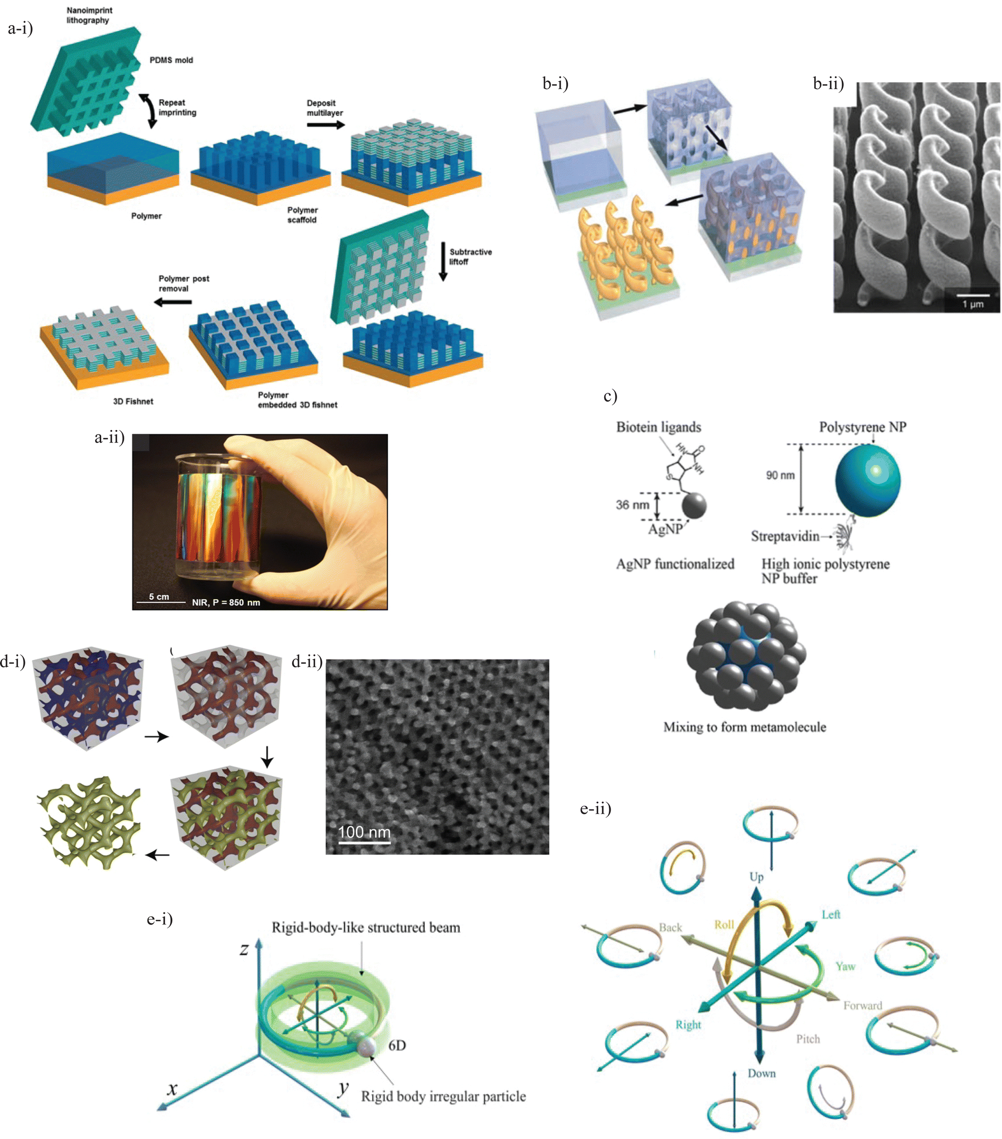 | ||
| Fig. 6 (a) Soft lithography. Process to fabricate negative index metamaterials (a-i) and large-area fishnet metamaterial on curved surface (a-ii). Panel reproduced from ref. 75 with permission from American Chemical Society, copyright 2014. (b) Direct laser writing. Process for fabrication of 3D gold helices (b-i), fabricated helices (b-ii). Panel reproduced from ref. 77 with permission from American Association for the Advancement of Science, copyright 2009. (c) Example of protein-assisted self-assembly. Panel reproduced from ref. 70 with permission from Springer Nature, copyright 2020. (d) Block-copolymer self-assembly. Process for gold metamaterial (d-i), SEM image of structure (d-ii). Panel reproduced from ref. 78 with permission from John Wiley and Sons, copyright 2012. (e) Manipulation of particles using structured light. Trapping of irregular particle (e-i) and the degrees of freedom achievable based on rigid body mechanics, including roll, pitch and yaw not available with conventional optical tweezers (e-ii). Panel reproduced from ref. 79 with permission from Photonics Research, copyright 2023. | ||
The creation of 3D structures with nanoimprint lithography can be cumbersome and time-consuming because the masks or molds for sequential layers must have good alignment.68,70 Although there has been work that has shown how 3D fabrication can be done in a single step,80 multiphoton lithography is a technique is not subject to alignment of a sequence of layers, making it more efficient and well-suited for 3D nanofabrication. The main mechanism behind multiphoton lithography, also referred to as direct laser writing, is photo-polymerization that requires the absorption of more than one photon and has the ability to polymerize arbitrary structures directly in a volume of material.68,81 Achieving sub-diffraction resolution that is around 100 nm is possible, although longitudinal resolution tends to be worse than lateral resolution.81,82 Fabrication time is related to scan speeds. Although scanning is a serial process, multiphoton lithography has been used with a microlens array for parallel fabrication.83 These lithographic techniques are applicable to the fabrication of microrobots that can be used in biological settings for targeted drug delivery and biosensing as well as remote sensing.84 In the area of metamaterials, direct laser writing has also been utilized85,86 with one unique example that highlights the 3D nature of these methods being an array of gold helices, shown in Fig. 6b.77 Two-step absorption, rather than two-photon absorption, has also been applied to 3D nanoprinting. This method is similar to multi-photon lithography but requires lower power and can use smaller, less expensive sources like a continuous wave laser rather than mode-locked pico- or femto-second lasers that are often employed for two-photon lithography and necessary to achieve efficient two-photon absorption.87 Further comparison between the two mechanisms is explored in the article by Hahn et al.
To further address large-scale fabrication, interference lithography exposes a large area simultaneously to create arrays on the order of square centimeters in area.88 A standing wave pattern is formed using two coherent beams in this technique and can achieve around 20 nm resolution using deep UV sources and immersion media.68,71 This technique is suitable for creating periodic arrays that are often used for metasurfaces or metamaterials.68,71,89
The variety of methods associated with lithography make it a useful approach for an array of microfabrication techniques with the main advantage being the high resolution. Different types of lithography can overcome challenges related to cost and material integration as well as 3D and large-scale production, although aspects like masks, molds, and post-processing procedures are still required.
As the OPAL platform demonstrates, optical tweezers are able to place particles at exact locations. This permits defects to be purposefully included in a structure and is not easily achieved using self-assembly.93 Advances in microfabrication using optical tweezers are aimed at improving particle manipulation through approaches like modification of the trapping beam. For example, holographic optical tweezers (HOTs) incorporate a spatial light modulator and can be used to create multiple trapping sites in both the axial and lateral planes.93,97 This type of optical tweezer has been used for automated assembly of microgranular crystals.98 An advantage to this technique is the ability to add an entire layer of particles at once rather than having to search for a single particle. However, complex image processing and associated algorithms are also often required,98,99 which may take more time and computational power than our population classification approach.
Structured light is another advancement that can be used with optical tweezers to increase the accessible degrees of freedom. In work by Zhu et al., structured light composed of two vortex beams traps two particles at a single point and is able to translate and rotate the system of particles about all three axes, shown in Fig. 6.79 This type of manipulation may be quite useful for complex manipulation of objects like nanorods, which are not spherically symmetrical.
The biochemical linking mechanism used with OPAL is one way to connect particles for complex structures. Other ways to accomplish this include photo-polymerization of material between particles, which can often require a setup with multiple lasers, and heating of particles to cause bonding, which may damage particles.93 This possible damage due to heating from high optical power is one disadvantage of optical tweezers fabrication, along with the need for a high numerical aperture objective, which can be expensive.100 To overcome these difficulties, other types of optical tweezers have been developed, such as opto-thermophoretic tweezers that can be used with a wider range of particles.93 The working principle of this branch of optical tweezers is that a temperature field is controlled using light, which affects the ionic depletants and permits manipulation of particles.93 Other types of tweezers systems use magnetic or acoustic fields for assembly.94 Additionally, work involving metasurfaces has gone towards developing such surfaces to replace traditional microscope objectives.100
While optical tweezers use optical forces to manipulate objects, mechanical manipulation of microscale objects has been shown using an atomic force microscopy cantilever with confocal microscopy for large field of view monitoring.101 An advantage to this mechanical manipulation compared to optical tweezers is the ability to physically alter organic objects via cutting, slicing, and bending, in addition to lifting and moving.101 These capabilities make this approach particularly well-suited for fabrication of components used in crystal-based organic photonic integrated circuits (OPIC) including passive and active waveguides, resonators, and cavities that are smaller than standard silicon photonic integrated circuits (PIC).101 This approach, termed “mechanophotonics,” is promising for expanding the functionality and types of materials used in PICs.
3.3 Future directions in fabrication
Other valuable fabrication methods exist beyond the mentioned lithography, self-assembly, and particle manipulation using optical or mechanical forces that are beyond the scope this article. Similar to how deciding which modeling or design approach to utilize depends on application and resources, the best fabrication method certainly will be determined by the required level of resolution, scalability, and accessible resources for the particular system. Looking forward, it is not hard to see how a combination of both top-down and bottom-up approaches may provide more flexibility in realizing nanophotonic designs in terms of feature size and shape as well as material integration.70 A recent example that highlights this idea applies focused ion beam milling, a lithographic approach that uses ions rather than electrons, to organic microcrystals created through techniques like self-assembly and sublimation for industrial-level production of crystal photonic cavities for PICs.102 Key aspects for future developments include scalability, functionality,73 and the ability to monitor the process in real time to assess and correct errors.1034 Emerging concepts and applications
The development and progress of the preceding computational methods and fabrication techniques will be integral for more advanced and innovative nanophotonic devices. This section will highlight several interesting concepts that are expected to be essential in such future devices and may also continue to be improved through design or fabrication, including work from our own lab related to metamaterials.4.1 Hyperbolic metamaterials
Previous metamaterial work that has been carried out within our lab studied a tunable hyperbolic metamaterial (HMM) operating at terahertz frequencies.104 Hyperbolic metamaterials are defined by hyperbolic iso-frequency curves and an anisotropic permittivity tensor, which can be achieved with a multi-layer stack of metal and dielectric layers. These materials are valuable in the area of super-resolution imaging because high-frequency information that is usually lost can be retained due to the formation of surface plasmon polaritons (SPPs) at metal/dielectric interfaces. Further, application of a hyperbolic metamaterial for super-resolution in the terahertz regime is valuable as the techniques that are employed for this purpose in the visible wavelengths are not applicable at these longer wavelengths. This work demonstrated that layers of high-density polyethylene (HDPE) and InSb achieve the properties of a hyperbolic metamaterial with tunable properties based on temperature and filling ratio, as shown using effective medium theory. Modeling of planar multilayer stacks verified transmission properties that agree with resonances seen in the permittivity as well as the confirmation of negative refractive index, seen in Fig. 7a.104 Lastly, modeling involving a cylindrical hyperlens formed with the multilayer HMM stack demonstrated the ability for such a device to image below the diffraction limit, shown in Fig. 7b. | ||
| Fig. 7 (a) and (b) Hyperbolic metamaterial. Modeling showing negative refractive index for planar multilayer stack (a-i) and (a-ii); resolution beyond diffraction limit for cylindrical hyperlens (b-i) and (b-ii). Panels (a) and (b) reproduced from ref. 104 with permission from Optical Society of America, copyright 2020. (c) Self-healing random lasers. Healing process after pressing (c-i), scratching (c-ii), stabbing (c-iii), and fracturing (c-iv). Panel reproduced from ref. 105 with permission from American Chemical Society, copyright 2019. (d) Mass migration. Formation of surface relief grating (d-i) and the writing and erasing process (d-ii). Panel reproduced from ref. 106 with permission from John Wiley and Sons, copyright 2019. (e) Tape lithography. SEM image of gold nanohole film made using tape lithography method on side of fiber (e-i) and corresponding areas on fiber (e-ii). Panel reproduced from ref. 107 with permission from Springer Nature, copyright 2018. (f) Quantum dot microlaser. Photographs of ring laser based on colloidal quantum dots using excitation power of 5.3, 74, 260, 600 μJ cm−2 (f, i-iv). Panel reproduced from ref. 108 with permission from American Chemical Society, copyright 2017. | ||
Another example of HMM work outside our lab used this type of metamaterial for random lasing. Random lasers accomplish lasing action through multiple scattering that is common in nanophotonic materials; these devices have the advantage of not requiring a cavity while maintaining high efficiency.109 The work by Lin et al. fabricated layers of gold and polymethyl methacrylate (PMMA) on a flexible substrate composed of paper and polydimethylsiloxane (PDMS) and used perovskite nanocrystals as a gain medium. The flexible HMMs were able to be rolled multiple times and with varying curvatures.110 These efforts can be applied to bio-sensing and wearable devices.110
4.2 Self-healing and reconfigurable materials and devices
The integration of nanophotonic devices in integrated photonic circuits and wearable devices expands the opportunities for such devices to become a part of daily life. An important consideration in the performance of such devices is how robust they are to damage that can affect optical properties. Self-healing materials offer a solution to help preserve the performance and lifetime of devices. Owing to the necessity of light sources in many photonic systems, work conducted by Hsu et al. combined the concept of a random laser, which does not rely on a traditional resonator, with a self-healing hydrogel to create a soft and self-healable random laser (SSRL).105 The healing ability of SSRLs stems from dynamical hydrogen bonds and this work demonstrated the reproducibility of the SSRLs to heal following repeated damage as well as after different damage types shown in Fig. 7c. A notable advantage to the self-healing lasers is not needing external stimuli for the healing process.Another interesting concept that relates to soft materials used for nanophotonic devices is the ability to reconfigure materials. This ability can make fabrication, especially prototyping, more efficient. Mass-migration is one tool that can be used to achieve such adaptable materials, as this review discusses,106 specifically photochromic isomerization. A brief overview of this process is that certain molecules respond to exposure to light in such a way that they will move based on the light intensity and polarization, resulting in structures such as the surface relief gratings schematically shown in Fig. 7d. A flat surface can later be recovered with thermal exposure or a specific polarization of light. Photo-polymerization is a similar type of technique extensively used for prototyping, but it is irreversible. As mentioned in Section 3.2.2, mechanophotonics is a promising approach for OPIC fabrication and has also demonstrated reconfigurability. This was shown through the formation of one photonic molecule (PM) created by two polystyrene microspheres (A–B) that were then separated and a new PM was formed with one of the previous microspheres and a new microsphere (B–C).111 This type of manipulation is especially useful for adjustment of building blocks throughout the assembly process and is distinct from linking mechanisms like that used in OPAL where permanent bonds form upon initial contact of particles. Beyond fabrication applications, reconfigurable materials are also ideal for rewritable photonic memory devices.112 The review by Lian et al. provides insight into this area including material platforms, architectures, computing mechanisms, and future applications.
4.3 Tape lithography fabrication
While more advanced fabrication techniques can often be associated with more cumbersome processes or expensive equipment, techniques that achieve high-level results with simple and versatile procedures are valuable from both an economical and accessibility standpoint. A poignant example of this is a lithography method implemented using common Scotch tape.107 This lithographic method starts with soft lithography (this is the most expensive part) to construct nanopatterns on a donor substrate which is followed by deposition of the chosen materials and then direct application and peeling of tape to transfer the patterned material.107 This technique can be applied to both dielectric and metallic materials for single layer or multilayer stacks with areas on the order of inches, demonstrated sub-100 nm resolution, and simultaneously provides a functional inverse structure within the donor substrate. Additionally, this is suitable for flexible applications, as was shown with flexible refractive index sensors and transfer of a gold nanohole film to an optical fiber shown in Fig. 7e.107 As also shown, this method is applicable to the fabrication of metamaterials.4.4 Quantum emitters, sensors, and information
Harnessing quantum effects promises to enable technological advances in areas like computing and communication. The synthesis of quantum phenomena with nanophotonics will further expand device capability and functionality. One example is colloidal quantum dots (CQD), which are semiconductor nanocrystals that display quantum effects, mainly the spatial confinement of charge carriers.113 This effect is significant because it allows for tuning of optical and electrical properties based on individual particle size, shape, and composition, which is well-established through synthesis procedures. Thin films can be made from such materials using techniques like lithography to create specific devices including waveguides, microlasers, and photodetectors for on-chip quantum applications.113 One interesting development showed that by using nanocrystals coated with a wider-bandgap material (core/shell quantum dots) in ring resonators, it is possible to control the lasing color by changing the excitation power as seen in Fig. 7f.108 CQDs are one instance of generating quantum responses; more material related to the intersection of nano- and quantum photonics, including quantum information, sensing, data storage, computing, circuits, metasurfaces, and lab on chip applications can be found in the cited reviews.114–1175 Future perspectives
As the examples provided throughout this Feature Article show, nanophotonics has applications in a multitude of fields and is driven by computational and fabrication capabilities. Currently, microscale precision in the design and construction of 3D structures composed of a single material is readily available, but a major current challenge is the ability to design and fabricate complex 3D structures with atomic precision from a wide range of different materials. And once these capabilities are achievable in small-scale, rapid prototyping platforms, mass production presents a whole new set of challenges.To address these challenges moving forward, a large part of the nanophotonic computation is expected to incorporate artificial intelligence such as deep learning, which should aid in exploring novel and nonintuitive device designs and configurations with decreased computational expense. The ability for this tool to consider a growing number of input design parameters while also being adaptable to a variety of contexts, from which new optimization schemes or algorithms may emerge, will make it especially useful. Fabrication considerations should also be standard in device design that has a physical application to ensure design outputs are realizable. In terms of fabrication, the combination of top-down and bottom-up approaches should aid in realizing high resolution and scalable devices. As nanophotonic components such as metasurfaces start to become more commonplace, the manufacturing of such tools is expected to move toward large-scale industry production, making many of the fabrication challenges presented here significant and not isolated to one community. Further, the pursuit of novel optical phenomena may lead to the use of unique or new materials, such as magneto-optical materials or van der Waals materials that were not considered here.
These advancements will contribute to devices with powerful and exciting new potential for nanoscale control of light. One major avenue for these improvements is for more compact devices, as seen with PICs, that can be mass-produced with greater ease and lower power consumption. An exciting prospect within this area is the ability to provide healthcare diagnostics through on-chip biological sensing and detection to rural areas that may not have adequate technology or resources otherwise. There is also no shortage of opportunities within the quantum domain in terms of advancing technological facets such as communications and computing as well as a general understanding of light–matter interaction.
6 Conclusions
Work from our lab has contributed to nanophotonic devices through efficient and accurate computation, design, and fabrication. On the computational side, an analysis of scattering and optical force calculations has shown that the complex permittivity of metallic nanoparticles accounts for the skin-depth effect more accurately than an effective volume correction. The angular spectrum method was adapted to allow fast and accurate computations of nanoscale light–matter interactions using a dipole matched transmission model. Our DDA-with-substrate approach compared three discrete dipole approximation methods and found the best results with a 1D cylindrical Green's function. Relevant computational and design approaches from other groups have relied upon the DDA, inverse design, boundary integral equations and augmented partial factorization to increase accuracy and efficiency. Artificial intelligence has already been incorporated in this field and will surely continue to develop as a tool for such technology.Experimentally, our optical positioning and linking (OPAL) platform uses optical tweezers and biochemical linking to manipulate micro- and nanoscale particles for the bottom-up fabrication of complex, heterogeneous nanostructures. Automation of the platform goes toward increasing throughput for even larger scale assemblies. Top-down, lithographic methods have shown great benefits in terms of resolution and variants have addressed drawbacks including time, scale, and cost. Self-assembly and advancements in optical tweezers continue to hold certain advantages for bottom-up fabrication, such as scalability and achievable complexity. Incorporating both top-down and bottom-up methods could be important for better resolution, more diverse material integration, larger scale, and reduced cost.
Other aspects of nanophotonic device design and application that may play an important role in the development of new technologies include metamaterial design, self-healing and reconfigurable materials, low-cost and simple fabrication, and quantum considerations.
The ability of nanophotonic devices to control light at subwavelength scales will enable applications ranging from biological imaging and sensing to computing.
Author contributions
N. S. performed data curation and wrote the original draft, including visualization. E. M. supervised, acquired funding, and reviewed and edited the manuscript.Data availability
No primary research results, software or code have been included and no new data were generated or analyzed as part of this review.Conflicts of interest
N. S. and E. M. are inventors on intellectual property related to the work discussed.Acknowledgements
Partial funding support was provided by the National Science Foundation grants ECCS-2045220 and ECCS-2114275. This paper was supported in part by a fellowship award under contract FA9550-21-F-0003 through the National Defense Science and Engineering Graduate (NDSEG) Fellowship Program, sponsored by the Air Force Research Laboratory (AFRL), the Office of Naval Research (ONR) and the Army Research Office (ARO).Notes and references
- A. F. Koenderink, A. Alù and A. Polman, Nanophotonics: shrinking light-based technology, Science, 2015, 348(6234), 516–521 CrossRef CAS PubMed.
- T. C. Ellis, S. Eslami and S. Palomba, More than a decade of progress, developments and challenges, Nanophotonics, 2024, 13(15), 2707–2739 CrossRef PubMed.
- R. Halir, P. J. Bock, P. Cheben, A. Ortega-Moñux, C. Alonso-Ramos and J. H. Schmid, et al., Waveguide sub-wavelength structures: a review of principles and applications, Laser Photonics Rev., 2015, 9(1), 25–49 CrossRef CAS.
- A. Ali, A. Mitra and B. Aïssa, Metamaterials and Metasurfaces: A Review from the Perspectives of Materials, Mechanisms and Advanced Metadevices, Nanomaterials, 2022, 12(6), 1027 CrossRef CAS PubMed.
- A. Karabchevsky, A. Katiyi, A. S. Ang and A. Hazan, On-chip nanophotonics and future challenges, Nanophotonics, 2020, 9(12), 3733–3753 CrossRef CAS.
- J. Yan, X. Liu, C. Ma, Y. Huang and G. Yang, All-dielectric materials and related nanophotonic applications, Mater. Sci. Eng., R, 2020, 141, 100563 CrossRef.
- D. G. Baranov, D. A. Zuev, S. I. Lepeshov, O. V. Kotov, A. E. Krasnok and A. B. Evlyukhin, et al., All-dielectric nanophotonics: the quest for better materials and fabrication techniques, Optica, 2017, 4(7), 814–825 CrossRef CAS.
- T. Taliercio and P. Biagioni, Semiconductor infrared plasmonics, Nanophotonics, 2019, 8(6), 949–990 CrossRef CAS.
- P. Deng, W. Hong and X. Hong-Xing, Metallic nanowires for subwavelength waveguiding and nanophotonic devices, Chin. Phys. B, 2013, 22(9), 097305 CrossRef.
- G. Rui and Q. Zhan, Tailoring optical complex fields with nano-metallic surfaces, Nanophotonics, 2015, 4(1), 2–25 CAS.
- P. N. Prasad, Polymer science and technology for new generation photonics and biophotonics, Curr. Opin. Solid State Mater. Sci., 2004, 8(1), 11–19 CrossRef CAS.
- J. Lee and S. Lee, Colloidal Optics and Photonics: Photonic Crystals, Plasmonics, and Metamaterials, Curr. Opt. Photonics, 2023, 7(6), 608–637 CAS.
- J. Valentine, S. Zhang, T. Zentgraf, E. Ulin-Avila, D. A. Genov and G. Bartal, et al., Three-dimensional optical metamaterial with a negative refractive index, Nature, 2008, 455(7211), 376–379 CrossRef CAS PubMed.
- V. M. Shalaev, W. Cai, U. K. Chettiar, H. K. Yuan, A. K. Sarychev and V. P. Drachev, et al., Negative index of refraction in optical metamaterials, Opt. Lett., 2005, 30(24), 3356–3358 CrossRef PubMed.
- S. Zhang, W. Fan, K. Malloy, S. Brueck, N. Panoiu and R. Osgood, Demonstration of metal-dielectric negative-index metamaterials with improved performance at optical frequencies, JOSA B, 2006, 23, 434–438 CrossRef CAS.
- J. Dintinger, S. Mühlig, C. Rockstuhl and T. Scharf, A bottom-up approach to fabricate optical metamaterials by self-assembled metallic nanoparticles, Opt. Mater. Express, 2012, 2(3), 269–278 CrossRef CAS.
- S. Mühlig, C. Rockstuhl, V. Yannopapas, T. Bürgi, N. Shalkevich and F. Lederer, Optical properties of a fabricated self-assembled bottom-up bulk metamaterial, Opt. Express, 2011, 19(10), 9607–9616 CrossRef PubMed.
- K. Svoboda and S. M. Block, Optical trapping of metallic Rayleigh particles, Opt. Lett., 1994, 19(13), 930–932 CrossRef CAS PubMed.
- W. Liu and E. McLeod, Accuracy of the Skin Depth Correction for Metallic Nanoparticle Polarizability, J. Phys. Chem. C, 2019, 123(20), 13009–13014 CrossRef CAS.
- M. Baker, W. Liu and E. McLeod, Accurate and fast modeling of scattering from random arrays of nanoparticles using the discrete dipole approximation and angular spectrum method, Opt. Express, 2021, 29(14), 22761–22777 CrossRef CAS PubMed.
- W. Liu and E. McLeod, Fast and accurate electromagnetic field calculation for substrate-supported metasurfaces using the discrete dipole approximation, Nanophotonics, 2023, 12(22), 4157–4173 CrossRef CAS PubMed.
- L. Ma, J. Li, Z. Liu, Y. Zhang, N. Zhang and S. Zheng, et al., Intelligent algorithms: new avenues for designing nanophotonic devices [Invited], Chin. Opt. Lett., 2021, 19(11), 011301 CrossRef.
- K. Kojima, M. H. Tahersima, T. Koike-Akino, D. K. Jha, Y. Tang and Y. Wang, et al., Deep Neural Networks for Inverse Design of Nanophotonic Devices, J. Lightwave Technol., 2021, 39(4), 1010–1019 CAS.
- C. Sideris, E. Garza and O. P. Bruno, Ultrafast Simulation and Optimization of Nanophotonic Devices with Integral Equation Methods, ACS Photonics, 2019, 6(12), 3233–3240 CrossRef CAS.
- W. Ma, Y. Xu, B. Xiong, L. Deng, R. W. Peng and M. Wang, et al., Pushing the Limits of Functionality-Multiplexing Capability in Metasurface Design Based on Statistical Machine Learning, Adv. Mater., 2022, 34(16), 2110022 CrossRef CAS PubMed.
- D. Gostimirovic, Y. Grinberg, D. X. Xu and O. Liboiron-Ladouceur, Improving Fabrication Fidelity of Integrated Nanophotonic Devices Using Deep Learning, ACS Photonics., 2023, 10(6), 1953–1961 CrossRef CAS.
- D. F. Carvalho, M. A. Martins, P. A. Fernandes and M. R. P. Correia, Coupling of plasmonic nanoparticles on a semiconductor substrate via a modified discrete dipole approximation method, Phys. Chem. Chem. Phys., 2022, 24(33), 19705–19715 RSC.
- Y. Zhao, M. Zhang, A. Alabastri and P. Nordlander, Fast Topology Optimization for Near-Field Focusing All-Dielectric Metasurfaces Using the Discrete Dipole Approximation, ACS Nano., 2022, 16(11), 18951–18958 CrossRef CAS PubMed.
- A. Siabi-Garjan, S. Kia, S. Mirzaee and A. Rostami, Highly sensitive silver-based localized surface plasmon resonance (LSPR) biosensor for microRNA-21 detection: discrete dipole approximation together with molecular polarizability method, Appl. Surf. Sci., 2023, 634, 157681 CrossRef CAS.
- A. Siabi-Garjan, A comprehensive study on the Rod-based plasmonic structures sensing using the modified discrete dipole approximation method, Photonics Nanostruct., Fundament. Appl., 2024, 58, 101224 CrossRef.
- K. Bi, Q. Wang, J. Xu, L. Chen, C. Lan and M. Lei, All-Dielectric Metamaterial Fabrication Techniques, Adv. Opt. Mater., 2021, 9(1), 2001474 CrossRef CAS.
- M. A. Yurkin, D. A. Smunev, A. E. Akhmetyanova and S. A. Glukhova, Capabilities of ADDA code for nanophotonics, J. Phys.: Conf. Ser., 2020, 1461(1), 012197 CrossRef.
- S. Molesky, Z. Lin, A. Y. Piggott, W. Jin, J. Vucković and A. W. Rodriguez, Inverse design in nanophotonics, Nat. Photonics, 2018, 12(11), 659–670 CrossRef CAS.
- T. W. Hughes, M. Minkov, I. A. D. Williamson and S. Fan, Adjoint Method and Inverse Design for Nonlinear Nanophotonic Devices, ACS Photonics, 2018, 5(12), 4781–4787 CrossRef CAS.
- E. Bayati, R. Pestourie, S. Colburn, Z. Lin, S. G. Johnson and A. Majumdar, Inverse Designed Metalenses with Extended Depth of Focus, 2020 Conf. Lasers Electro-Optics (CLEO), 2020, 7(4), 873–878 CAS.
- U. Haeusler, M. Seidling, P. Yousefi and P. Hommelhoff, Boosting the Efficiency of Smith-Purcell Radiators Using Nanophotonic Inverse Design, ACS Photonics, 2022, 9(2), 664–671 CrossRef CAS.
- N. K. Georgieva, S. Glavic, M. H. Bakr and J. W. Bandler, Feasible adjoint sensitivity technique for EM design optimization, IEEE Trans. Microwave Theory Tech., 2002, 50(12), 2751–2758 CrossRef.
- C. M. Lalau-Keraly, S. Bhargava, O. D. Miller and E. Yablonovitch, Adjoint shape optimization applied to electromagnetic design, Opt. Express, 2013, 21(18), 21693–21701 CrossRef PubMed.
- K. Wang, X. Ren, W. Chang, L. Lu, D. Liu and M. Zhang, Inverse design of digital nanophotonic devices using the adjoint method, Photonics Res., 2020, 8(4), 528–533 CrossRef CAS.
- X. Zheng, C. Mystilidis, A. Xomalis and G. A. E. Vandenbosch, A Boundary Integral Equation Formalism for Modeling Multiple Scattering of Light from 3D Nanoparticles Incorporating Nonlocal Effects, Adv. Theory Simul., 2022, 5(12), 2200485 CrossRef CAS.
- E. Garza and C. Sideris, Fast Inverse Design of 3D Nanophotonic Devices Using Boundary Integral Methods, ACS Photonics, 2023, 10(4), 824–835 CAS.
- H. C. Lin, Z. Wang and C. W. Hsu, Fast multi-source nanophotonic simulations using augmented partial factorization, Nat. Comput. Sci., 2022, 2(12), 815–822 CrossRef PubMed.
- S. Li, H. C. Lin and C. W. Hsu, Fast Multichannel Inverse Design through Augmented Partial Factorization, ACS Photonics, 2024, 11(2), 378–384 CrossRef CAS PubMed.
- K. Demertzis, G. D. Papadopoulos, L. Iliadis and L. Magafas, A Comprehensive Survey on Nanophotonic Neural Networks: Architectures, Training Methods, Optimization, and Activations Functions, Sensors, 2022, 22(3), 720 CrossRef CAS PubMed.
- A. Khaireh-Walieh, D. Langevin, P. Bennet, O. Teytaud, A. Moreau and P. R. Wiecha, A newcomers guide to deep learning for inverse design in nano-photonics, Nanophotonics, 2023, 12(24), 4387–4414 CrossRef PubMed.
- F. Monticone and A. Alù, Metamaterial, plasmonic and nanophotonic devices, Rep. Prog. Phys., 2017, 80(3), 036401 CrossRef PubMed.
- X. Shi, T. Qiu, J. Wang, X. Zhao and S. Qu, Metasurface inverse design using machine learning approaches, J. Phys. D: Appl. Phys., 2020, 53(27), 275105 CrossRef CAS.
- L. A. K. Schulte, M. Butz, M. Becker, B. Risse and C. Schuck, Accelerating finite-difference frequency-domain simulations of inverse designed structures in nanophotonics using deep learning, J. Opt. Soc. Am. B, 2024, 41(4), 1039–1046 CrossRef CAS.
- E. Adibnia, M. Ghadrdan and M. A. Mansouri-Birjandi, Nanophotonic structure inverse design for switching application using deep learning, Sci. Rep., 2024, 14(1), 21094 CrossRef CAS PubMed.
- F. Ferranti, Feature-based machine learning for the efficient design of nanophotonic structures, Photonics Nanostruct., Fundam. Appl., 2022, 52, 101077 CrossRef.
- S. Yu, T. Zhang, J. Dai and K. Xu, Hybrid inverse design scheme for nanophotonic devices based on encoder-aided unsupervised and supervised learning, Opt. Express, 2023, 31(24), 39852–39866 CrossRef PubMed.
- C. Yeung, B. Pham, Z. Zhang, K. T. Fountaine and A. P. Raman, Hybrid supervised and reinforcement learning for the design and optimization of nanophotonic structures, Opt. Express, 2024, 32(6), 9920–9930 CrossRef CAS PubMed.
- A. Y. Piggott, J. Petykiewicz, L. Su and J. Vucković, Fabrication-constrained nanophotonic inverse design, Sci. Rep., 2017, 7(1), 1786 CrossRef PubMed.
- A. Ashkin, J. M. Dziedzic, J. E. Bjorkholm and S. Chu, Observation of a single-beam gradient force optical trap for dielectric particles, Opt. Lett., 1986, 11(5), 288–290 CrossRef CAS PubMed.
- A. Ashkin, Optical Trapping And Manipulation Of Neutral Particles Using Lasers: A Reprint Volume With Commentaries, World Scientific Publishing Company, Singapore, Singapore, 2006 Search PubMed.
- C. Bradac, Nanoscale Optical Trapping: A Review, Adv. Opt. Mater., 2018, 6(12), 1800005 CrossRef.
- J. E. Melzer and E. McLeod, Fundamental Limits of Optical Tweezer Nanoparticle Manipulation Speeds, ACS Nano, 2018, 12(3), 2440–2447 CrossRef CAS PubMed.
- J. E. Melzer and E. McLeod, Assembly of multicomponent structures from hundreds of micron-scale building blocks using optical tweezers, Microsyst. Nanoeng., 2021, 7(1), 45 CrossRef PubMed.
- J. E. Melzer, N. K. Shultz and E. McLeod, Microscale Additive Assembly with Optical Tweezers, In: 2022 Conference on Lasers and Electro-Optics, CLEO 2022 – Proceedings, 2022.
- C. Li, T. Lohrey, P. D. Nguyen, Z. Min, Y. Tang and C. Ge, et al., Part-per-Trillion Trace Selective Gas Detection Using Frequency Locked Whispering-Gallery Mode Microtoroids, ACS Appl. Mater. Interfaces, 2022, 14(37), 42430–42440 CrossRef CAS PubMed.
- Y. Xu, A. M. Stanko, C. S. Cerione, T. D. Lohrey, E. McLeod and B. M. Stoltz, et al., Low Part-Per-Trillion, Humidity Resistant Detection of Nitric Oxide Using Microtoroid Optical Resonators, ACS Appl. Mater. Interfaces, 2024, 16(4), 5120–5128 CrossRef CAS PubMed.
- L. Chen, C. Li, Y. M. Liu, J. Su and E. McLeod, Simulating robust far-field coupling to traveling waves in large three-dimensional nanostructured high-Q microresonators, Photonics Res., 2019, 7(9), 967–976 CrossRef CAS.
- C. Li, L. Chen, E. McLeod and J. Su, Dark mode plasmonic optical microcavity biochemical sensor, Photonics Res., 2019, 7(8), 939–947 CrossRef CAS.
- S. Suebka, E. McLeod and J. Su, Ultra-high-Q free-space coupling to microtoroid resonators, Light: Sci. Appl., 2024, 13(1), 75 CrossRef CAS PubMed.
- L. Chen, C. Li, Y. Liu, J. Su and E. McLeod, Three-Dimensional Simulation of Particle-Induced Mode Splitting in Large Toroidal Microresonators, Sensors, 2020, 20(18), 5420 CrossRef CAS PubMed.
- N. Shultz and E. McLeod, Fully automated optical tweezers using backscattered signal for large-scale 3D microfabrication, In preparation.
- G. Dolling, M. Wegener, C. M. Soukoulis and S. Linden, Negative-index metamaterial at 780 nm wavelength, Opt. Lett., 2006, 32(1), 53–55 CrossRef PubMed.
- A. Boltasseva and V. M. Shalaev, Fabrication of optical negative-index metamaterials: recent advances and outlook, Metamaterials, 2008, 2(1), 1–17 CrossRef.
- V. Hahn, P. Kiefer, T. Frenzel, J. Qu, E. Blasco and C. Barner-Kowollik, et al., Rapid Assembly of Small Materials Building Blocks (Voxels) into Large Functional 3D Metamaterials, Adv. Funct. Mater., 2020, 30(26), 1907795 CrossRef CAS.
- Y. Chen, B. Ai and Z. J. Wong, Soft optical metamaterials, Nano Convergence, 2020, 7(1), 18 CrossRef CAS PubMed.
- S. R. J. Brueck, Optical and Interferometric Lithography – Nanotechnology Enablers, Proc. IEEE, 2005, 93(10), 1704–1721 CAS.
- H. T. Chen, W. J. Padilla, J. M. O. Zide, A. C. Gossard, A. J. Taylor and R. D. Averitt, Active terahertz metamaterial devices, Nature, 2006, 444(7119), 597–600 CrossRef CAS PubMed.
- G. Yoon, I. Kim and J. Rho, Challenges in fabrication towards realization of practical metamaterials, Microelectron. Eng., 2016, 163, 7–20 CrossRef CAS.
- S. Y. Chou, P. R. Krauss and P. J. Renstrom, Nanoimprint lithography, J. Vac. Sci. Technol., B: Microelectron. Process. Phenom., 1996, 14(6), 4129–4133 CrossRef CAS.
- L. Gao, K. Shigeta, A. Vazquez-Guardado, C. J. Progler, G. R. Bogart and J. A. Rogers, et al., Nanoimprinting Techniques for Large-Area Three-Dimensional Negative Index Metamaterials with Operation in the Visible and Telecom Bands, ACS Nano, 2014, 8(6), 5535–5542 CrossRef CAS PubMed.
- X. Cao, Y. Xiao, Q. Dong, S. Zhang, J. Wang and L. Wang, et al., Tuning Metasurface Dimensions by Soft Nanoimprint Lithography and Reactive Ion Etching, Adv. Photonics Res., 2022, 3(11), 2200127 CrossRef CAS.
- J. K. Gansel, M. Thiel, M. S. Rill, M. Decker, K. Bade and V. Saile, et al., Gold Helix Photonic Metamaterial as Broadband Circular Polarizer, Science, 2009, 325(5947), 1513–1515 CrossRef CAS PubMed.
- S. Vignolini, N. A. Yufa, P. S. Cunha, S. Guldin, I. Rushkin and M. Stefik, et al., A 3D Optical Metamaterial Made by Self-Assembly, Adv. Mater., 2012, 24(10), OP23–OP27 CrossRef CAS PubMed.
- L. Zhu, Y. Tai, H. Li, H. Hu, X. Li and Y. Cai, et al., Multidimensional optical tweezers synthetized by rigid-body emulated structured light, Photonics Res., 2023, 11(9), 1524–1534 CrossRef.
- N. Koo, M. Schmidt, T. Mollenhauer, C. Moormann, F. Schlachter and H. Kurz, Fabrication of MOSFETs by 3D soft UV-nanoimprint, Microelectron. Eng., 2012, 97, 85–88 CrossRef CAS.
- Y. L. Zhang, Q. D. Chen, H. Xia and H. B. Sun, Designable 3D nanofabrication by femtosecond laser direct writing, Nano Today, 2010, 5(5), 435–448 CrossRef CAS.
- J. E. Melzer and E. McLeod, 3D Nanophotonic device fabrication using discrete components, Nanophotonics, 2020, 9(6), 1373–1390 CrossRef.
- F. Formanek, N. Takeyasu, T. Tanaka, K. Chiyoda, A. Ishikawa and S. Kawata, Three-dimensional fabrication of metallic nanostructures over large areas by two-photon polymerization, Opt. Express, 2006, 14(2), 800–809 CrossRef CAS PubMed.
- J. Li and M. Pumera, 3D printing of functional microrobots, Chem. Soc. Rev., 2021, 50(4), 2794–2838 RSC.
- I. Sakellari, X. Yin, M. L. Nesterov, K. Terzaki, A. Xomalis and M. Farsari, 3D Chiral Plasmonic Metamaterials Fabricated by Direct Laser Writing: The Twisted Omega Particle, Adv. Opt. Mater., 2017, 5(16), 1700200 CrossRef.
- S. Liu, X. Wang, J. Ni, Y. Cao, J. Li and C. Wang, et al., Optical Encryption in the Photonic Orbital Angular Momentum Dimension via Direct-Laser-Writing 3D Chiral Metahelices, Nano Lett., 2023, 23(6), 2304–2311 CrossRef CAS PubMed.
- V. Hahn, T. Messer, N. M. Bojanowski, E. R. Curticean, I. Wacker and R. R. Schröder, et al., Two-step absorption instead of two-photon absorption in 3D nanoprinting, Nat. Photonics, 2021, 15(12), 932–938 CrossRef CAS.
- N. Feth, C. Enkrich, M. Wegener and S. Linden, Large-area magnetic metamaterials via compact interference lithography, Opt. Express, 2007, 15(2), 501–507 CrossRef PubMed.
- S. Brueck, Large-Area Nanophotonics Fabricated by Interferometric Lithography, 2006, vol. 1, pp. 86–89 Search PubMed.
- U. R. Gabinet and C. O. Osuji, Optical materials and metamaterials from nanostructured soft matter, Nano Res., 2019, 12(9), 2172–2183 CrossRef CAS.
- B. Gong, X. Zhao, Z. Pan, S. Li, X. Wang and Y. Zhao, et al., A visible metamaterial fabricated by self-assembly method, Sci. Rep., 2014, 4(1), 4713 CrossRef PubMed.
- A. Baron, A. Aradian, V. Ponsinet and P. Barois, [INVITED] Self-assembled optical metamaterials, Opt. Laser Technol., 2016, 82, 94–100 CrossRef CAS.
- A. Kotnala and Y. Zheng, Digital Assembly of Colloidal Particles for Nanoscale Manufacturing, Part. Part. Syst. Charact., 2019, 36(8), 1900152 CrossRef PubMed.
- K. Eftekhari, B. V. Parakhonskiy, D. Grigoriev and A. G. Skirtach, Advances in Nanoarchitectonics: A Review of “Static” and “Dynamic” Particle Assembly Methods, Materials, 2024, 17(5), 1051 CrossRef CAS PubMed.
- N. Lee, R. Kim, J. Y. Kim, J. B. Ko, S. H. K. Park and S. O. Kim, et al., Self-Assembled Nano-Lotus Pod Metasurface for Light Trapping, ACS Photonics, 2021, 8(6), 1616–1622 CrossRef CAS.
- G. Lin, Y. An, H. Ding, H. Zhao, J. Wang and S. Chen, et al., Scalable fabrication of self-assembled GeSn vertical nanowires for nanophotonic applications, Nanophotonics, 2023, 12(2), 219–228 CrossRef CAS PubMed.
- E. R. Shanblatt and D. G. Grier, Extended and knotted optical traps in three dimensions, Opt. Express, 2011, 19(7), 5833–5838 CrossRef CAS PubMed.
- S. Chizari, M. P. Lim, L. A. Shaw, S. P. Austin and J. B. Hopkins, Automated Optical-Tweezers Assembly of Engineered Microgranular Crystals, Small, 2020, 16(25), 2000314 CrossRef CAS PubMed.
- O. E. C. Gould, S. J. Box, C. E. Boott, A. D. Ward, M. A. Winnik and M. J. Miles, et al., Manipulation and Deposition of Complex, Functional Block Copolymer Nanostructures Using Optical Tweezers, ACS Nano, 2019, 13(4), 3858–3866 CrossRef CAS PubMed.
- J. Xiao, T. Plaskocinski, M. Biabanifard, S. Persheyev and A. Di Falco, On-Chip Optical Trapping with High NA Metasurfaces, ACS Photonics, 2023, 10(5), 1341–1348 CrossRef CAS PubMed.
- R. Chandrasekar, Mechanophotonics—Mechanical Micromanipulation of Single-Crystals toward Organic Photonic Integrated Circuits, Small, 2021, 17(24), 2100277 CrossRef CAS PubMed.
- V. V. Pradeep, M. Chosenyah, E. Mamonov and R. Chandrasekar, Crystal photonics foundry: geometrical shaping of molecular single crystals into next generation optical cavities, Nanoscale, 2023, 15(29), 1222–12226 RSC.
- X. Zhao, Bottom-up fabrication methods of optical metamaterials, J. Mater. Chem., 2012, 22(19), 9439–9449 RSC.
- H. Zhang, Z. Jiao and E. Mcleod, Tunable terahertz hyperbolic metamaterial slabs and super-resolving hyperlenses, Appl. Opt., 2020, 59(22), G64–G70 CrossRef PubMed.
- Y. T. Hsu, C. T. Tai, H. M. Wu, C. F. Hou, Y. M. Liao and W. C. Liao, et al., Self-Healing Nanophotonics: Robust and Soft Random Lasers, ACS Nano, 2019, 13(8), 8977–8985 CrossRef CAS PubMed.
- K. Kim, H. Park, K. J. Park, S. H. Park, H. H. Kim and S. Lee, Light-Directed Soft Mass Migration for Micro/Nanophotonics, Adv. Opt. Mater., 2019, 7(16), 1900074 CrossRef.
- Q. Wang, W. Han, Y. Wang, M. Lu and L. Dong, Tape nanolithography: a rapid and simple method for fabricating flexible, wearable nanophotonic devices, Microsyst. Nanoeng., 2018, 4(1), 31 CrossRef PubMed.
- B. le Feber, F. Prins, E. De Leo, F. T. Rabouw and D. J. Norris, Colloidal-Quantum-Dot Ring Lasers with Active Color Control, Nano Lett., 2018, 18(2), 1028–1034 CrossRef CAS PubMed.
- D. S. Wiersma, The physics and applications of random lasers, Nat. Phys., 2008, 4(5), 359–367 Search PubMed.
- H. I. Lin, C. C. Wang, K. C. Shen, M. Y. Shalaginov, P. K. Roy and K. P. Bera, et al., Enhanced laser action from smart fabrics made with rollable hyperbolic metamaterials, npj Flexible Electron., 2020, 4(1), 20 Search PubMed.
- M. Annadhasan, A. V. Kumar, D. Venkatakrishnarao, E. A. Mamonov and R. Chandrasekar, Mechanophotonics: precise selection, assembly and disassembly of polymer optical microcavities via mechanical manipulation for spectral engineering, Nanoscale Adv., 2020, 2(12), 5584–5590 RSC.
- C. Lian, C. Vagionas, T. Alexoudi, N. Pleros, N. Youngblood and C. Ríos, Photonic (computational) memories: tunable nanophotonics for data storage and computing, Nanophotonics, 2022, 11(17), 3823–3854 CrossRef CAS PubMed.
- J. Chen and K. Rong, Nanophotonic devices and circuits based on colloidal quantum dots, Mater. Chem. Front., 2021, 5(12), 452–4537 RSC.
- J. Chang, J. Gao, I. E. Zadeh, A. W. Elshaari and V. Zwiller, Nanowire-based integrated photonics for quantum information and quantum sensing, Nanophotonics, 2023, 12(3), 339–358 CrossRef CAS PubMed.
- J. M. Arrazola, V. Bergholm, K. Brádler, T. R. Bromley, M. J. Collins and I. Dhand, et al., Quantum circuits with many photons on a programmable nanophotonic chip, Nature, 2021, 591(7848), 54–60 CrossRef CAS PubMed.
- A. S. Solntsev, G. S. Agarwal and Y. S. Kivshar, Metasurfaces for quantum photonics, Nat. Photonics, 2021, 15(5), 327–336 CrossRef CAS.
- J. Xavier, D. Yu, C. Jones, E. Zossimova and F. Vollmer, Quantum nanophotonic and nanoplasmonic sensing: towards quantum optical bioscience laboratories on chip, Nanophotonics, 2021, 10(5), 1387–1435 CrossRef CAS.
| This journal is © The Royal Society of Chemistry 2025 |