
 Open Access Article
 This Open Access Article is licensed under a
 Creative Commons Attribution 3.0 Unported Licence
Interface phenomena and emerging functionalities in ferroelectric oxide based heterostructures
Yifei
Hao
 ,
Tianlin
Li
and
Xia
Hong
*
,
Tianlin
Li
and
Xia
Hong
*
Department of Physics and Astronomy & Nebraska Center for Materials and Nanoscience, University of Nebraska-Lincoln, Lincoln, NE 68588-0299, USA. E-mail: xia.hong@unl.edu
First published on 3rd February 2025
Abstract
Capitalizing on the nonvolatile, nanoscale controllable polarization, ferroelectric perovskite oxides can be integrated with various functional materials for designing emergent phenomena enabled by charge, lattice, and polar symmetry mediated interfacial coupling, as well as for constructing novel energy-efficient electronics and nanophotonics with programmable functionalities. When prepared in thin film or membrane forms, the ferroelectric instability of these materials is highly susceptible to the interfacial electrostatic and mechanical boundary conditions, resulting in tunable polarization fields and Curie temperatures and domain formation. This review focuses on two types of ferroelectric oxide-based heterostructures: the epitaxial perovskite oxide heterostructures and the ferroelectric oxides interfaced with two-dimensional van der Waals materials. The topics covered include the basic synthesis methods for ferroelectric oxide thin films, membranes, and heterostructures, characterization of their properties, and various emergent phenomena hosted by the heterostructures, including the polarization-controlled metal–insulator transition and magnetic anisotropy, negative capacitance effect, domain-imposed one-dimensional graphene superlattices, programmable second harmonic generation, and interface-enhanced polar alignment and piezoelectric response, as well as their applications in nonvolatile memory, logic, and reconfigurable optical devices. Possible future research directions are also outlined, encompassing the synthesis via remote epitaxy and oxide moiré engineering, incorporation of binary ferroelectric oxides, realization of topological properties, and functional design of oxygen octahedral rotation.
1. Introduction
Ferroelectrics possess nonvolatile, spontaneous polarization that is switchable via an external electric field (Fig. 1). When they are prepared in thin film forms, the ferroelectric free energy is highly susceptible to the electrostatic and mechanical boundary conditions, which can be utilized to engineer the polar properties and control domain formation.1–3 The heterostructures interfacing ferroelectrics with other nanoscale functional materials thus present a versatile platform for designing emergent ferroic orders and exploring novel control mechanisms that are not viable in single-phase materials. Leveraging the voltage-controlled nature and nanoscale programmable polarization, ferroelectric thin films have been widely adopted to construct energy-efficient electronic devices, including ferroelectric field effect transistors (FeFETs),4 ferroelectric tunnel junctions (FTJs),5 memristors,6 and negative capacitance (NC) transistors,7 which are promising building blocks for developing low-power memory and logic applications as well as neuromorphic computing. Their polar properties have also been exploited in intriguing mechanical8 and optical9 applications. | ||
| Fig. 1 Overview of research on ferroelectric perovskite oxide-based heterostructures, including material systems, emergent phenomena, and potential device applications. Pup/Pdown: polarization up/down. | ||
Compared with the widely studied ferroelectric polymer and van der Waals (vdW) materials, ferroelectric perovskite oxides are known for their large polarization, high dielectric constant, high ferroelectric Curie temperature (TC), low coercive field (Ec), and unit-cell-scale sharp domain walls (DWs).1 For ferroelectric perovskite thin films and membranes, the interfacial layers play a critical role in determining the material parameters and even affecting the ferroelectric instability. Capitalizing on the interfacial coupling mediated by charge, strain, and polar symmetry, ferroelectric oxides have been utilized to modulate the electronic, magnetic, and optical properties of the neighboring materials.4,10–14 Various emergent phenomena have been reported in ferroelectric oxide-based heterostructures, including polarization-controlled quantum phase transitions,15,16 polar vortices,17,18 negative capacitance mode,19,20 enhanced polar alignment,21,22 periodic domain structure imposed superlattices,23 and unconventional nonlinear optical filtering effects.24,25 The ability to synthesize single crystalline ferroelectric oxide membranes26–29 and stack them with controlled twist angles29 lifts the lattice constraints for building multifunctional heterointerfaces and opens up the opportunity to develop oxide-based twistronics. The advancements in the growth of crystalline ferroelectric perovskites on conventional semiconductors such as Si30,31 and Ge32 herald the potential to integrate these emergent functionalities with the mainstream semiconductor industry.
In this feature article, we focus on two types of ferroelectric oxide-based heterostructures, the epitaxial complex oxide heterostructures and the ferroelectric thin films and membranes interfaced with two-dimensional (2D) van der Waals materials, discussing the basic synthesis methods and property characterization and surveying a range of interface phenomena and emerging functionalities. In Section 2, we discuss the synthesis and characterization of different types of heterostructures. Section 3 summarizes the effects of the interfacial layer on the ferroelectric properties of epitaxial oxide thin films and freestanding membranes. Section 4 focuses on the epitaxial ferroelectric oxide heterostructures, discussing the polarization control of the electronic and magnetic properties of correlated oxides, the ferroelectric-to-dielectric transition, domain formation, and transient NC effect in ferroelectric/dielectric oxide heterostructures, as well as related device concepts such as Mott FeFETs and all-oxide FTJs. Section 5 centers on the ferroelectric/2D van der Waals heterostructures, discussing the ferroelectric field effect, domain induced superlattice modulation, tuning of second harmonic generation, and enhanced polar alignment and piezoelectric response in 2D ferroelectrics, as well as highlighting the potential applications in electron lensing, NC FETs, and programmable nonlinear optical filters. Section 6 summarizes the research progress and provides an outlook on possible future directions, such as novel synthesis via remote epitaxy and oxide moiré engineering, incorporation of doped ferroelectric hafnia and zirconia, realization of topological properties, and functional design of oxygen octahedral rotation.
2. Materials synthesis and characterization
2.1 Epitaxial ferroelectric oxide heterostructures
The rapid development of advanced physical vapor deposition (PVD) techniques enables scalable growth of high quality epitaxial thin films of ferroelectric oxides. For perovskite transition metal oxides, their structural and chemical similarities allow the combination of ferroelectric oxides with various functional oxides, ranging from dielectrics to Mott insulators, magnets, and superconductors, into high-quality epitaxial heterostructures.11 The atomic registration between interfacial constituent layers can not only eliminate dangling bonds, minimizing defect formation, but also enable novel lattice design via controlling lattice strain33 and oxygen octahedral rotation.34 In addition to the charge mediated coupling mechanism, strain-induced lattice distortion and migration of defects such as oxygen vacancies can also have a profound impact on the physical properties.For epitaxial complex oxide thin film deposition, widely used PVD techniques35 include molecular-beam epitaxy (MBE), pulsed laser deposition (PLD), and off-axis radio-frequency (RF) magnetron sputtering. In this paper, we center on the discussions of epitaxial ferroelectric thin films and heterostructures prepared via the off-axis RF magnetron sputtering approach. Examples include the ferroelectric/correlated oxide and ferroelectric/dielectric perovskite heterostructures. Compared with the MBE and PLD methods, magnetron sputtering has the advantages of low growth temperature, compatibility with industrial scale deposition, and low cost. The sputtering technique has recently been utilized to prepare polar nitride perovskites,36 which broadens the class of materials viable for exploring polarization-based phenomena and device applications.37 One limitation of the sputtering growth is that the strong magnetic field precludes the implementation of the reflection high-energy electron diffraction (RHEED) technique for in situ characterization of sample crystallinity and growth mode. Efforts have been made to incorporate RHEED into sputtering via special sputtering chamber design, such as adopting antisymmetric sputter sources.38
The PVD techniques can yield single crystalline thin films and heterostructures with high crystallinity, atomically flat surfaces, and unit-cell-level precise control of film thickness. Fig. 2 shows the surface, structural, and chemical properties of ferroelectric PbZr0.2Ti0.8O3 (PZT) interfaced with dielectric oxide SrTiO3 (STO) and strongly correlated oxides such as RNiO3 (RNO with R = Sm, Nd, or La) and La0.67Sr0.33MnO3 (LSMO). These samples possess smooth surface morphology, as revealed by atomic force microscopy (AFM). Fig. 2(a) shows the AFM image taken on a 50 nm PZT/10 nm LSMO heterostructure deposited on a (001) STO substrate with a root-mean-square (RMS) roughness of 4–5 Å.23 X-ray diffraction (XRD) measurements of these heterostructures reveal the (001) growth of all layers (Fig. 2(b) and (c)).23,39Fig. 2(c) shows the XRD spectra taken on a series of PZT/STO heterostructures with about 100 nm total thickness deposited on 10 nm LaNiO3 (LNO) buffered STO.39 Regardless of the layer thickness, the c-axis of PZT is about 4.17 ± 0.1 Å, consistent with the strained value on STO, showing that epitaxial strain can sustain in 100 nm thickness films.
 | ||
| Fig. 2 Characterization of epitaxial PZT heterostructures. (a) AFM topography image and (b) XRD θ–2θ scan taken on 50 nm PZT/10 nm LSMO on (001) STO, with a fit to the Laue oscillations around the (001) peak of PZT (red line). Reproduced from ref. 23 with permission from American Physical Society, copyright 2024. (c) XRD θ–2θ scans taken on PZT/STO heterostructures with a total thickness of about 100 nm deposited on LNO buffered STO substrates with different PZT and STO layer thickness ratios (r = tPZT/tSTO). (d) XRR performed on a PZT/STO heterostructure. Reproduced from ref. 39 with permission from American Physical Society, copyright 2021. (e) HRSTEM and (f) in-plane lattice constants of different layers normalized to that of STO substrate for a PZT/3 nm SNNO/2 nm LSMO heterostructure. Reproduced from ref. 40 with permission from Wiley-VCH GmbH, copyright 2017. (g) HRSTEM (left panel) and EELS element mapping performed on a PZT/3 uc LNO/3 uc LSMO heterostructure. Reproduced from ref. 41 with permission from Springer Nature, copyright 2023. (h) EELS line scans for five elements taken on the sample shown in (e) and (f). Reproduced from ref. 40 with permission from Wiley-VCH GmbH, copyright 2017. | ||
Even though real-time monitoring of the growth rate is not available for these sputtered samples, the highly smooth sample surfaces/interfaces allow post-growth thickness characterization via either the Laue oscillations around the main Bragg peaks (Fig. 2(b) and (c))23,39 or X-ray reflectivity (XRR) (Fig. 2(d))39 measurements, which can be used to calibrate the deposition rate. Transmission electron microscopy (TEM) studies confirm that precise thickness control has been achieved. Fig. 2(e) shows the high-resolution scanning TEM (HRSTEM) image of a PZT/3 nm Sm0.5Nd0.5NiO3 (SNNO)/2 nm LSMO heterostructure,40 which reveals high crystallinity and atomically sharp interfaces. The in-plane lattice constant for each atomic layer has been deduced from the TEM data, confirming that the entire heterostructure is fully strained to the STO substrate (Fig. 2(f)).40Fig. 2(g) shows the electron energy loss spectroscopy (EELS) elemental mapping of a PZT/1.2 nm LNO/1.2 nm LSMO heterostructure,41 showing that the interfaces are also chemically sharp. The line profiles of the EELS data (Fig. 2(h)) indicate that the diffusion of interfacial atoms is typically within one-to-two unit cell (uc) scale.40,41
2.2 Free-standing ferroelectric oxide membranes
Recent developments in the synthesis of single crystalline complex oxide membranes42,43 further broaden the material design portfolio for ferroelectric oxide-based heterostructures, opening up new avenues for exploring novel interface phenomena and achieving tailored functionalities.25,28,29,44–47 In particular, it is possible to construct heterostructures with the same constituents either in the epitaxial heterointerface form or via direct contact of membranes. Comparing the physical properties of these two types of systems helps differentiate the effects of electrostatic and mechanical boundary conditions on the ferroelectric instability in perovskite thin films. Building twisted ferroelectric oxide heterostructures further broadens the parameter space for engineering novel polar states,29 which are not bound by the intrinsic crystal symmetry. Epitaxial ferroelectric oxide thin films can be suspended from the substrate via depositing on a water soluble layer such as Sr3Al2O6 (SAO) (Fig. 3(a)) followed by water etching28,42 or through selected chemical etching of a buffer layer such as (La,Sr)MnO3.29,44 The freestanding membranes can then be transferred on any designated base layer using Gel-Film28 or PMMA47 with precision control of position and orientation (Fig. 3(b)). | ||
| Fig. 3 Preparation and characterization of PZT membranes. (a) Schematic of a PZT/SAO heterostructure on STO. (b) Schematic of dry transfer of a PZT membrane on a designated base layer. (c) XRD θ–2θ scan and (d) AFM topography image taken on 50 nm PZT/20 nm SAO on (001) STO. (e) XRD θ–2θ scan of the same sample after water etching of the SAO layer. (f) AFM topography image a PZT flake transferred on a LSMO/STO base layer. Inset: Optical image of the flake. Reproduced from ref. 28 with permission from American Chemical Society, copyright 2023. | ||
Fig. 3(c)–(f) compares the crystallinity and surface roughness of a 50 nm PZT film deposited on 20 nm SAO buffered STO before and after water-etching. The epitaxial heterostructure possesses single crystalline (001) PZT and SAO layers with no impurity phases (Fig. 3(c)) and smooth surface morphology with an RMS roughness of about 5 Å (Fig. 3(d)). After water-etching, the SAO peaks disappear, while the suspended PZT layer retains the crystallinity (Fig. 3(e)) and shows the same c-axis lattice constant of 4.15 Å, suggesting that the PZT membrane remains fully strained even after suspension from the substrate. Fig. 3(f) shows the AFM image of a 20 nm PZT membrane transferred on a LSMO/STO base layer. The flake exhibits clear ripples, with the RMS roughness (∼1 nm) significantly higher than the roughness of the base layer (∼4 Å) (Table 1). In contrast, the 20 nm PZT/10 nm LSMO membrane on LSMO/STO exhibits a surface roughness similar to the base layer, suggesting that atomic bonding with the LSMO layer effectively reduces rippling.
| Sample | Buffer/base layer | Surface roughness (film thickness) (nm) | E c (MV cm−1) | T C (°C) | |
|---|---|---|---|---|---|
| P up | P down | ||||
| Epitaxial PZT | LSMO | 0.4 (50) | −0.5 | +1.1 | 775 ± 25 |
| LaNiO3 | 0.2 (50) | −0.56 | +0.38 | 738 ± 12 | |
| SrIrO3 | 0.3 (50) | −0.1 | +0.36 | 775 ± 25 | |
| PZT membrane | Au | 2.0 (20) | −3.0 | +1.7 | 763 ± 12 |
| LSMO | 1.0 (20) | −1.70 | +1.09 | 725 ± 25 | |
| MoS2 | 0.3 (20) | −1.60 | +0.75 | 588 ± 12 | |
| PZT/LSMO membrane | Au | 0.8 (20) | −0.18 | +0.74 | |
| LSMO | 0.5 (20) | −0.26 | +0.28 | ||
| MoS2 | 0.4 (20) | −0.6 | +1.01 | ||
2.3 Ferroelectric oxide/2D van der Waals heterostructures
Integrating ferroelectric oxides with 2D van der Waals materials can enable functional design of the electronic, mechanical, and optical responses via ferroelectric field effect doping, strain modulation, and nanoscale domain control.4,14 The van der Waals layers can be interfaced with single-crystalline49–53 and polycrystalline ferroelectric thin films,54–56 ferroelectric single crystals,57,58 and ferroelectric oxide membranes.25,28,44–46 Compared with the epitaxial thin films, large-scale, low-cost synthesis of polycrystalline ferroelectric oxide films can be achieved by chemical vapor deposition (CVD) methods such as the metal–organic CVD59 approach and the sol–gel method.60 While these techniques are desirable for industrial processing, the polycrystalline samples exhibit compromised polarization and high density structural defects such as grain boundaries.The 2D van der Waals layers can be prepared on the ferroelectric oxide substrates via direct mechanical exfoliation,49,50 dry transfer,23,25,28 or direct CVD growth.58 The direct mechanical exfoliation method exploits adhesive tape to peel off 2D atomic layers from high-quality single crystals and lay the resulting flakes directly on the ferroelectric substrates.61 It preserves to the maximum extent the intrinsic properties of the 2D materials, while the limitations include low yield, lack of thickness control, presence of tape residue, and difficulty in identifying atomically thin flakes on ferroelectric oxides due to low optical contrast.49,56 To increase the yield and flake size for mechanical exfoliation, substrate treatments with oxygen plasma62 or metal-film-coating63 have been developed to enhance the interaction between the substrate and van der Waals materials. By pre-patterning interaction-enhanced regions, it is possible to have 2D vdW flakes directly exfoliated onto specific locations on the substrate, resulting in complex architectures unattainable with conventional exfoliation and dry-transfer methods. While these interaction-enhancement approaches have been successfully applied to a wide range of 2D materials to achieve up to millimeter-scale exfoliation,62–65 they may alter the surface chemistry of the ferroelectric oxides or produce undesired interfacial layers, which compromise the device functionality.
In the dry-transfer method, viscoelastic polymer films such as polydimethylsiloxane (PDMS),66 polypropylene carbonate (PPC),67,68 and polycarbonate (PC)69 serve as transfer stamps to pick up and drop down pre-prepared 2D vdW flakes, which facilitates precise positioning and stacking-order control for heterostructure fabrication. The pick-up and drop-down processes are controlled by adjusting the vitrification of polymer films at different temperatures, while the transfer process is guided by an actuated x–y–z–θ-stage, enabling sub-micron-scale precision in alignment and placement of 2D flakes on the oxide substrate, as well as control over interlayer twist angles. The dry nature of the transfer process ensures that the interface remains uncontaminated, as it avoids solvent exposure until the final cleaning step for removing polymer residues. Additionally, encapsulation with air-stable top layers such as hexagonal boron nitride (h-BN) protects the vdW surface from direct exposure to the ambient conditions, which is critical for preserving the intrinsic properties of 2D materials that are sensitive to moisture.70
Bottom-up synthesis techniques, such as CVD, physical vapor transport, and MBE, have also been developed for fabricating 2D vdW flakes, thin films, and heterostructures.71–73 For example, monolayer MoS2 has been directly grown on a periodically poled LiNbO3 substrate, which shows a preferred growth on the Pup domains.58 It is conceivable that scalable synthesis of 2D vdW thin films directly on the ferroelectric substrate can facilitate the development of industrial applications of ferroelectric oxide/2D vdW heterostructures. A major material challenge is that most of these techniques involve high temperature synthesis in high/ultrahigh vacuum, which can exceed the structural phase transition temperatures of some widely used ferroelectric oxides (e.g., BaTiO3)74 and introduce oxygen vacancies,75 therefore compromising the device performance.
3. Interface effects on ferroelectric properties
3.1 Epitaxial ferroelectric thin films
Various ferroelectric properties of ferroelectric oxide thin films, including polarization, Ec, TC, and domain wall roughness and creep behaviors, have been investigated using electrical measurements and scanning probe microscopy. The results reveal the profound effects of electrostatic and mechanical boundary conditions on ferroelectricity and domain formation. Fig. 4(a) shows the characterization of polarization vs. electric field (P–E) loops taken on an Au/100 nm PZT/10 nm LaNiO3 capacitor, where the polarization is calculated by integrating the charging and discharging current through the circuit upon polarization switching.39 The deduced remanent polarization is about 78 μC cm−2, consistent with those obtained from Hall effect measurements of epitaxial FeFETs.41,76 The coercive field increases with increasing frequency (f) of the bias voltage (Vbias) wave, with Ec exhibiting a power-law dependence on f (Fig. 4(b)),39 which can be well described by the domain nucleation and growth dominated polarization switching process.77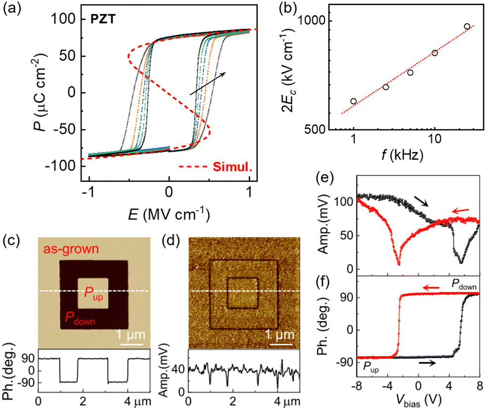 | ||
| Fig. 4 Ferroelectric properties of PZT thin films. (a) P–E loops at different Vbias frequencies, and (b) 2Ecvs. f for an Au/100 nm PZT/10 nm LaNiO3 capacitor on STO. Reproduced from ref. 39 with permission from American Physical Society, copyright 2021. (c)–(f) PFM studies of a 50 nm PZT/10 nm LSMO heterostructure on STO. (c) PFM phase and (d) amplitude images of concentric square domains. (e) PFM amplitude and (f) phase switching hysteresis. Reproduced from ref. 48 with permission from American Physical Society, copyright 2021. | ||
Conductive AFM and piezoresponse force microscopy (PFM) have been used to assess polarization switching, write/image domain structures, and quantify the piezoelectric coefficients. Fig. 4(c) and (d) shows the PFM images of concentric square domains written on a PZT/LSMO heterostructure via conductive AFM, which shows that the as-grown sample is uniformly polarized in the Pup state.48Fig. 4(e) and (f) shows the PFM switching hysteresis taken on this sample, which reveals a smaller coercive voltage for the Pup state than that for the Pdown state, consistent with the as-grown polarization, confirming that the Pup state is energetically favorable. The polarization asymmetry has been widely observed in epitaxial PZT thin films and depends sensitively on the choice of correlated oxide electrodes (Table 1).48 Quantitatively analyzing the PFM amplitude response vs. Vbias below the coercive field can yield the piezoelectric coefficient.21,22
PFM studies have also been utilized to assess TC, polarization switching dynamics, and the static configuration of DWs in epitaxial ferroelectric thin films. Due to the compressive strain, epitaxial PZT thin films deposited on (001) SrTiO3 substrates normally exhibit significantly higher TC compared with the bulk value (TC ∼ 450 °C78). Fig. 5(a) shows the PFM images of stripe domains written on a PZT/LSMO heterostructure on SrTiO3, where the sample has been heated at progressively higher temperatures and quenched rapidly to room temperature.48 The domain structure remains stable after thermal-quench (TQ) cycles at temperatures of up to 600 °C. Bubble domains start to emerge at 650 °C, while the originally straight DWs become barely recognizable at 750 °C. Similar results have been observed in PZT films with LaNiO3 and SrIrO3 (SIO) bottom electrodes, showing that TC for PZT strained on SrTiO3 is above 700 °C (Table 1).48 The high thermal stability makes epitaxial PZT thin films viable for high temperature applications.
 | ||
| Fig. 5 PFM characterization of ferroelectric perovskite oxide thin films. (a) PFM phase images of a domain structure in PZT/LSMO on STO at selected TQ temperatures. Reproduced from ref. 48 with permission from American Physical Society, copyright 2021. (b) PFM amplitude response vs. time with fits to t−α taken on a 15 nm SZTO film on Ge. The power exponents are labelled. Adapted from ref. 32 with permission from American Chemical Society, copyright 2017. (c) DW roughness correlation relation B(L) vs. L for 50 nm PZT films on 10 nm correlate oxide electrodes. Inset: Schematic of a rough DW. (d) ζ vs. TQ temperature. (e) Schematic of thermally activated DW motion in a disorder energy landscape tilted by an external field. (f) Schematic ζ–T diagram. Reproduced from ref. 48 with permission from American Physical Society, copyright 2021. | ||
For industrial applications, there has been extensive research interest in integrating ferroelectric perovskites with conventional semiconductors.79,80 Besides canonical ferroelectrics such as PZT30 and BaTiO3,31 perovskite oxides that are non-ferroelectric in bulk such as STO81 and Sr(Zr,Ti)O3 (SZTO)32 can develop a ferroelectric relaxor phase in strained thin films. Fig. 5(b) shows the PFM amplitude response of Pup and Pdown domains patterned on a 15 nm SZTO film deposited on Ge. The amplitude signal relaxes initially with a power-law time dependence t−α and then stabilizes at about 10 hours, remaining stable after 48 hours of domain writing. The exponents are α = 0.22 for the Pup state and α = 0.23 for the Pdown state, which are consistent with strained STO that exhibits relaxor behavior.82
Despite the similar TC, the PZT films deposited on different correlated oxide electrodes exhibit distinct thermal evolution of DW roughness due to the collective contributions of interfacial screening condition and defect migration. For ferroelectrics, the DW roughness carries important information about the dimensionality, disorder type, and nature of interaction of the system,83,84 which can be quantitatively assessed by calculating the correlation function of the relative transverse displacement (u) of two points along the DW separated by a distance L (Fig. 5(c) inset):  , which averages over position and disorder distribution. Treating DW as an elastic manifold in a disordered medium, B(L) exhibits a power-law dependence on L, B(L) ∝ L2ζ, where ζ is the roughness exponent. Previous PFM studies have shown that the DW roughening of epitaxial PZT thin films exhibits 2D random bond (RB) disorder dominated behavior with long range dipole interaction (ζ2D,RB = 0.31) at room temperature85 and evolves to a one-dimensional (1D) thermal roughening (ζ1D,TF = 0.5) dominated behavior at high temperatures.48,86 DW roughening due to 1D RB behavior (ζ1D,RB = 2/3) has been theoretically predicted87 but has been scarcely observed experimentally in epitaxial thin films, which can be affected by the artificial domain writing process, the ambient screening condition, and the relative energy and length scales of DW elasticity, thermal fluctuation, and disorder pinning.87–90
In ref. 48, Wang et al. investigated the effect of the correlated oxide electrode on the thermal evolution of DW roughness in PZT. Fig. 5(d) shows ζ vs. TQ temperature for 50 nm PZT films deposited on SrTiO3 buffered by 10 nm LSMO, LaNiO3, and SrIrO3 electrodes. For all samples, the ζ values exhibit 2D RB behavior at room temperature and approach 1D thermal roughening behavior close to TC. The DW growth can be treated as the creep motion of particles in a disorder energy landscape, where thermal fluctuation promotes the de-trapping of DW from the local pinning potential (Fig. 5(e)). The transition temperatures where ζ starts to deviate from ζ2D,RB (Tcr) and where ζ approaches ζ1D,TF (Tth) correspond to the lower and higher bound of the pinning energy, respectively (Fig. 5(f)).48 PZT on LSMO exhibits the highest transition temperatures, while PZT on SrIrO3 exhibits the lowest, which can be attributed to the effects of lattice distortion and the oxygen migration induced interfacial biasing field. In the former mechanism, LSMO possesses the largest oxygen octahedral rotation and SrIrO3 is the closest to the cubic structure that is closely matched with PZT.91–94 For the latter, the oxygen migration energy is the lowest in LSMO and the highest in SrIrO3, which can result in different trapping energies at the PZT interface.95–98 For devices using ferroelectric domains as the information storage unit, the DW roughness determines how closely two bits can be placed without interfering with each other, its temperature response determines the thermal stability of the bit, and Ec determines the writing voltage. Understanding the effect of the electrode material is thus critical for designing the storage density, operation temperature, and energy consumption of PZT-based memory applications, as further illustrated in the ferroelectric membranes.
3.2 Ferroelectric membranes
In ref. 28, Wu et al. examined the Ec (Fig. 6(a) and (b)) and TC (Fig. 6(c)) of PZT and PZT/LSMO membranes prepared on three types of base layers with distinct screening capacities and surface roughness, the metallic Au, correlated LSMO, and semiconducting MoS2 (Table 1). For single-layer 20 nm PZT membranes, Ec is the highest on Au and lowest on MoS2 (Ec(Au) > Ec(LSMO) > Ec(MoS2)), which has been attributed to the change in membrane surface roughness and base layer screening capacity. The rippling of membranes induces a flexoelectric effect, which suppresses DW motion and enhances Ec.26 The base layer with low conductivity can lead to a high depolarization field, suppress the ferroelectric double well energy, and thus reduce Ec. For comparison, the membranes of PZT/LSMO heterostructures possess a smoother surface morphology compared with the PZT membranes and exhibit significantly smaller Ec on the same type of base layer (Fig. 6(b)). Among these samples, the PZT/LSMO membrane on the LSMO base layer exhibits symmetric switching with the smallest average Ec value (Table 1). This is significantly lower than those of PZT membranes on LSMO and epitaxial PZT/LSMO heterostructures, despite the same screening electrode (LSMO), clearly illustrating the critical role of the mechanical boundary conditions (e.g., interface roughness and epitaxy) in determining the polarization switching dynamics.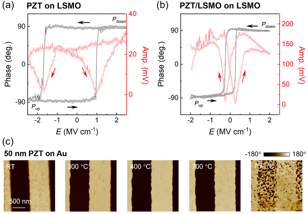 | ||
| Fig. 6 PFM characterization of PZT and PZT/LSMO membranes. (a) and (b) PFM phase and amplitude switching hysteresis taken on a 20 nm PZT membrane (a) and a 20 nm PZT/10 nm LSMO membrane (b) on LSMO base layers. (c) PFM phase images of stripe domains on a 50 nm PZT membrane on Au at selected TQ temperatures showing a TC > 750 °C. Reproduced from ref. 28 with permission from American Chemical Society, copyright 2023. | ||
Fig. 6(c) shows the PFM images of thermally quenched stripe domains written on a 50 nm PZT membrane on Au. For all three types of base layers, the PZT membranes exhibit enhanced TC well exceeding the bulk value (Table 1), consistent with the XRD result showing that the membranes can retain the strain state (Fig. 3(c) and (e)). The membrane on MoS2 possesses the lowest TC (>575 °C), suggesting that the atomically smooth van der Waals type interface may facilitate strain relaxation. At room temperature, PZT membranes thicker than 10 nm and PZT/LSMO membranes on all types of base layers exhibit 2D RB disorder dominated behavior with ζ close to ζ2D,RB (Fig. 7(a)). For the 10 nm PZT membrane on Au, ζ approaches ζ1D,TF. As the Au film possesses the highest surface roughness, the rippled membrane is partially decoupled from the substrate, which may release it from interface-induced DW pinning, allowing 1D thermal fluctuation dominated DW roughening. Similar to that of epitaxial PZT films (Fig. 5(d)), ζ increases with increasing TQ temperatures (Fig. 7(b)). For the 50 nm PZT membrane on MoS2, ζ increases to ζ1D,TF at Tth ∼ 500 °C. Despite the much higher TC, PZT membranes on LSMO and Au base layers exhibit a much lower Tcr. The ζ values quickly exceed ζ1D,TF and approach ζ1D,RB, suggesting a DW creep behavior within the quasi-equilibrium-nucleation model.87 Such 1D RB disorder dominated DW roughness has not been observed in epitaxial PZT films at large length scales,88 and the equilibrium configuration may be established in the PZT membranes due to partial decoupling from the LSMO and Au base layers. The distinct Ec and thermal evolution of DW roughness for PZT membranes on different base layers illustrate the convoluted effects of rippling induced flexoelectric effects, local strain distribution, interface induced DW pinning, and mobility of charged disorders in determining DW motion.28
 | ||
| Fig. 7 DW roughness in PZT membranes. (a) ζ vs. PZT thickness at room temperature for PZT and PZT/LSMO membranes on different base layers. (b) ζ vs. TQ temperature for 50 nm PZT membranes on different base layers. Reproduced from ref. 28 with permission from American Chemical Society, copyright 2023. | ||
4. Epitaxial ferroelectric oxide heterostructures
4.1 Ferroelectric/correlated oxide heterostructures
 | ||
| Fig. 8 Ferroelectric field effect in PZT-gated correlated channels. (a) Device schematic. (b) R□(T) of 4 nm La0.8Sr0.2MnO3 on STO for both polarization states. Adapted from ref. 100 with permission from American Physical Society, copyright 2019. (c) R□(T) of 2.5 nm and 4 nm SNNO channels on LaAlO3 for both polarization states. Inset: Resistance on/off ratio vs. temperature. Reproduced from ref. 40 with permission from Wiley-VCH GmbH, copyright 2017. (d) R□(T) of a 1.5 nm LaNiO3 channel for both polarization states. (e) Resistance on/off ratio of single-layer RNiO3 channels vs. channel thickness at 300 K. Adapted from ref. 41 with permission from Springer Nature, copyright 2023. | ||
The optimal channel thickness for the ferroelectric field effect modulation is determined by the interfacial charge screening effect and electronic finite size effect. As switching the polarization field yields a fixed 2D density modulation, 2P = Δn2D, the fractional change of 3D carrier density in the channel scales inversely with the channel thickness. On the other hand, the thickness scaling cannot be sustained when the film becomes electrically dead, a phenomenon widely observed in epitaxial correlated oxide thin films,16,41,102,103 as strongly localized charges cannot provide proper screening for the polarization field, which leads to poor retention behavior for the off state.40,76Fig. 8(c) shows the R□(T) of 4 nm and 2.5 nm Sm0.5Nd0.5NiO3 devices for both polarization states of PZT.40 At 300 K, the resistance switching ratio ΔR/Ron for the 2.5 nm channel is about one order of magnitude higher than that of the 4 nm SNNO. For 4 nm SNNO, ΔR/Ron exhibits a peak at 160 K, which is in the vicinity of the metal–insulator transition temperature. Such transition is absent in the 2.5 nm channel as it is below the electrical dead layer thickness. Close to the electrical dead layer thickness, it is possible to induce a carrier density-driven metal–insulator transition via the ferroelectric field effect.16Fig. 8(d) shows the R□(T) of a 1.5 nm, or 4 uc, LaNiO3 channel for both polarization states of the PZT gate. Bulk LaNiO3 is a correlated metal, while the Pdown state of PZT depletes holes from LaNiO3 and induces an insulating state.41
Fig. 8(e) summarizes the channel thickness (tRNO) dependence of ΔR/Ron at 300 K in single-layer RNiO3 channels.41 NdNiO3 (NNO), SNNO, and SmNiO3 (SNO) are charge-transfer type Mott insulators with progressively lower charge itinerancy due to a higher degree of lattice distortion.91,104 Despite the distinct metallicity, the LaNiO3, NdNiO3, and SNNO channels exhibit highly consistent exponential growth of ΔR/Ron with decreasing tRNO until the electrical dead layer thickness is reached, clearly pointing to the interfacial charge screening scenario. LaNiO3 possesses the smallest electrical dead layer thickness of about 2 uc, and the 2 uc LaNiO3 channel exhibits the largest resistance modulation. The corresponding resistance on–off ratio is about 17, which is the highest room temperature value reported for oxide FeFETs with single-layer Mott channels.41 The maximum ΔR/Ron are smaller in NNO (2.5 uc channel) and SNNO (6.5 uc channel), which can be attributed to the larger electrical dead layer thicknesses. The field effect is negligibly small in SNO, which is insulating in bulk at 300 K. The channel thickness scaling behavior reflects the convoluted effects of carrier density modulation and charge itinerancy in determining the ferroelectric field effect, while strain-induced lattice distortion, interfacial lattice/orbital effects, and size-induced dimensionality crossover can all affect the metallicity of the system.105–107 Understanding their impacts is critical for developing device applications such as the Mott FeFETs and all-oxide FTJs discussed below.
One solution to reduce the net carrier density in the Mott channel without causing severe depolarization in the ferroelectric gate is to exploit the charge transfer effect between two correlated oxides to create a tailored density profile in the Mott channel. It has been shown that inserting an LSMO buffer layer with intrinsically low carrier density in RNO3-based Mott FeFETs can significantly enhance the resistance on–off ratio by orders of magnitude.40,41 The interfacial charge transfer between RNiO3 and LSMO corresponds to the valence change of Ni3+ + Mn3+ → Ni2+ + Mn4+. Fig. 9 shows the high-angle-annular-dark-field (HAADF) STEM image and EELS elemental mapping of Mn L spectra taken on a PZT/3 uc LNO/3 uc LSMO heterostructure. The atomic layer-by-atomic layer mapping of the Mn valence state (Fig. 9(c) and (d)) reveals about 0.7 eV shift of the Mn L3 peak position, corresponding to 0.06 e−/Mn transfer from Mn to Ni ions. XAS and XPS studies also point to a charge transfer of 0.08–0.09 e−/Mn at the Sm0.5Nd0.5NiO3/LSMO interface,40 and the experimental results are well corroborated by density functional theory calculations.40,41 The charge transfer effectively reduces the carrier density in RNiO3 within 1–2 uc at the LNO/LSMO interface (Fig. 9(d)), while the high carrier density at the PZT/LNO interface is sustained.
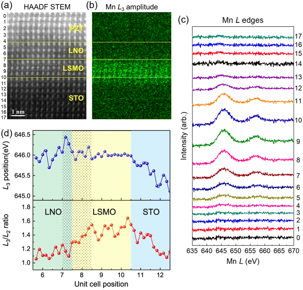 | ||
| Fig. 9 TEM characterization of a PZT/3 uc LNO/3 uc LSMO heterostructure. (a) Cross-sectional HRSTEM image. (b) EELS elemental mapping of Mn. (c) Layer-by-layer EELS spectra of the Mn L edge. The unit cell positions are labeled in (a). (d) Mn L3 peak position (top) and L3/L2 intensity ratio (bottom) as a function of unit cell position. Adapted from ref. 41 with permission from Springer Nature, copyright 2023. | ||
Fig. 10 compares the resistance switching of FeFETs with single-layer and bilayer correlated channels with similar total channel thickness. For a 4 uc LaNiO3 channel (Fig. 10(a)) and a 3 uc LNO/1 uc LSMO channel (Fig. 10(b)), the resistance on/off ratio (roff/on) in the bilayer channel is more than 40 times higher. Increasing the LNO single-layer channel thickness to 5 uc leads to smaller resistance modulation (Fig. 10(c)), as the bottom layer can be treated as a shunting resistor. On the other hand, the ferroelectric field effect in the LNO/LSMO bilayer cannot be modeled as parallel conduction of two independent channels. Increasing the LSMO layer thickness by 1 uc significantly enhances, rather than attenuates, the resistance modulation (Fig. 10(d)), clearly illustrating the effect of interface synergy between LNO and LSMO. Fig. 10(e) summarizes the ΔR/Ron of RNO/LSMO bilayer channels with different layer thickness combinations, which increases exponentially with decreasing total channel thickness (ttot). The universal channel thickness scaling behavior for the Mott FeFETs with both single-layer and bilayer channels clearly testify to the interfacial screening nature of the ferroelectric field effect. For the same ttot, roff/on in the bilayer channel can be over two orders of magnitude higher than that of single-layer RNiO3, pointing to a highly effective approach for designing the ferroelectric field effect. Fig. 10(f) compares the maximum room temperature ΔR/Ronvs. channel thickness (tchannel) obtained on epitaxial complex oxide FeFETs with different correlated oxide channels, including cuprate,111,112 cobaltate,113 manganite,16,114 ruthenate,115 single-layer nickelate,40,41 and bilayer RNiO3/LSMO40,41 channels. The PZT/2.5 uc LNO/2 uc LSMO device exhibits a record high room temperature roff/on of 385.4, well exceeding the state-of-the-art results for MRAM.116
 | ||
| Fig. 10 Room temperature resistance modulation in ferroelectric-gated LNO and LNO/LSMO channels. (a) and (b) R□ switching upon pulsed gate voltage Vg taken on 4 uc LNO (a) and 4 uc LNO/1 uc LSMO (b) channels. (c) and (d) R□vs. Vg switching hysteresis taken on 5 uc LNO (c) and 3 uc LNO/2 uc LSMO (d) channels. (e) ΔR/Ronvs. ttot in RNO/LSMO channels, with the layer thickness in the unit of uc labeled. (f) Maximum ΔR/Ronvs. tchannel for various correlated oxide channels. Inset: ΔR/Ronvs. Vg switching hysteresis taken on a PZT/2.5 uc LNO/2 uc LSMO sample. Adapted from ref. 41 with permission from Springer Nature, copyright 2023. | ||
For the bilayer channels, the presence of LSMO further provides an extended screening layer for minimizing the depolarization field in PZT, yielding excellent retention compared with the single-layer devices (Fig. 10(c) and (d)). For the 3 uc LNO/2 uc LSMO channel, roff/on stabilizes at 55% of the initial value after a few hours (Fig. 11(a)).41 The cycling behavior shows a characteristic three-stage fatigue behavior consistent with previous reports of PZT thin films:117 (I) slow fatigue stage until 106 cycles, (II) logarithmic stage until 108 cycles, and (III) saturated stage settling at 76% of the initial value until 1010 cycles (Fig. 11(b)). The high frequency conductivity has been investigated by microwave impedance microscopy (MIM) (Fig. 11(c)), which shows that the on–off ratio is stable up to 1 GHz (Fig. 11(d)), confirming that the resistance switching originates from the modulation of carrier density rather than ionic defects (e.g., oxygen vacancies).118 The high on–off ratio,41 excellent retention and endurance,41 fast switching,113 robust high frequency response,118 and potential for constructing epitaxial three-dimensional architectures119 make the Mott FeFETs highly competitive for developing nonvolatile memories and neuromorphic computing, which can be potentially integrated with the main stream Si technology.30–32
 | ||
| Fig. 11 Room temperature performance of RNiO3-based Mott FeFETs. (a) Retention and (b) cycling behaviors of a PZT/3 uc LNO/2 uc LSMO sample. Reproduced from ref. 41 with permission from Springer Nature, copyright 2023. (c) MIM imaginary (top) and real (bottom) signal images (bottom) of a 3 uc LNO/2 uc LSMO channel underneath square domains of PZT, and (d) the extracted conductance on/off ratio vs. imaging frequency. Adapted from ref. 118 with permission from AIP Publishing, copyright 2024. | ||
In ref. 99, Zhang et al. showed that a giant room temperature ER can be achieved in all-oxide FTJs by pairing a correlated metal LaNiO3 with a narrow bandgap Mott insulator Sr3Ir2O7 as electrodes (Fig. 12(a) and (b)). Switching the PZT polarization in LaNiO3/PZT/Sr3Ir2O7 FTJs into the Pup and Pdown states results in high (Ion) and low (Ioff) tunneling current, respectively. At room temperature, the ER, defined as (Ion − Ioff)/Ioff, is 6500% (1000%) for the FTJ with 4 nm (2.8 nm) PZT barrier (Fig. 12(c)), which is one to three orders of magnitude higher than those of all-oxide FTJs with correlated oxide electrodes and similar tunnel barrier configurations (Fig. 12(d)).126–128 The giant enhancement has been attributed to the polarization induced metal–insulator transition in the interfacial Sr3Ir2O7, which is feasible as Sr3Ir2O7 is a narrow-gap Mott insulator with a bandgap of about 0.1 eV,129 leading to a highly asymmetric tunnel barrier energy profile for the Pup and Pdown states (Fig. 12(e)). Moreover, Sr3Ir2O7 exhibit moderate conductivity even in the insulating state, effectively reducing the depolarization field. For the FTJ with thicker (4 nm) barrier, no apparent relaxation has been observed in the tunneling conductance. At 100 K, the ER ratio increases to 1.62 × 10⁵% (1.46 × 10⁵%) for the FTJ with 4 nm (2.8 nm) PZT barrier (Fig. 12(c)), which has been attributed to the pyroelectric increase of ferroelectric polarization.23 The larger coercive field and the suppressed on-state relaxation behavior even for the FTJ with ultrathin (2.8 nm) barrier are consistent with the suppressed domain wall depinning of PZT at low temperature.48 The giant ER, nonvolatile reversible switching, and superb retention make the all-oxide FTJs with narrow bandgap Mott electrodes highly competitive for nonvolatile memory and neuromorphic computing applications.
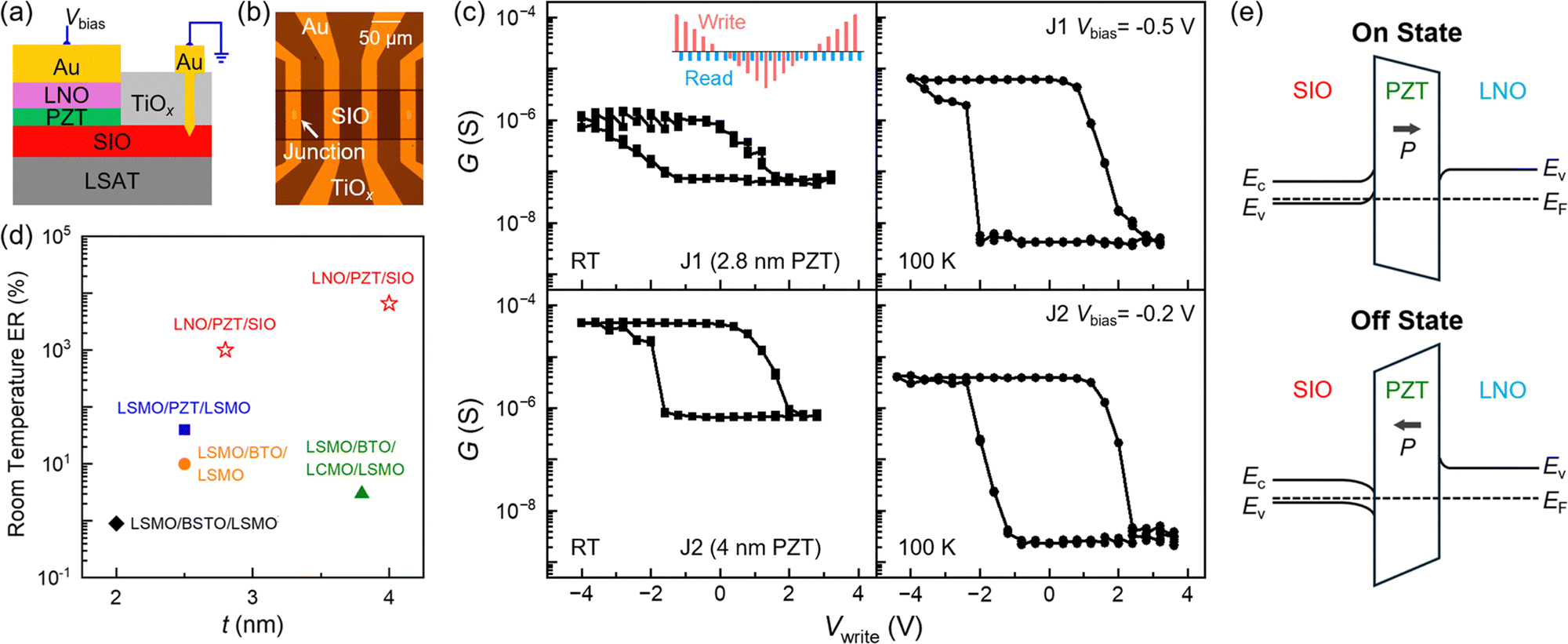 | ||
| Fig. 12 Fabrication and characterization of LaNiO3/PZT/Sr3Ir2O7 FTJs. (a) Device schematic. SIO: Sr3Ir2O7. (b) Optical image of a sample patterned with four tunnel junctions. (c) Tunneling conductance G vs. writing voltage Vwrite at room temperature and 100 K for FTJs with 2.8 nm and 4 nm PZT barriers. (d) Room temperature ER vs. tunnel barrier thickness t for various all-oxide FTJs.126–128 LCMO: (La,Ca)MnO3. BTO: BaTiO3. BSTO: (Ba,Sr)TiO3. (e) Schematic band diagrams for the on and off states. Adapted from ref. 99 with permission from AIP Publishing, copyright 2024. | ||
In ref. 100, Rajapitamahuni et al. demonstrated the manipulation of magnetic anisotropy energy (MAE) in 4 nm La0.8Sr0.2MnO3 on (001) SrTiO3via the ferroelectric field effect. For nanoscale magnetic materials, where the sample volume is too small for detection with conventional magnetometry, the anisotropic magnetoresistance (AMR) and planar Hall effect (PHE) are sensitive tools for assessing the magnetic state.134,135 In the coherent rotation model, the PHE and AMR resistance are given by:135
RPHE = (R‖ − R⊥)sin![[thin space (1/6-em)]](https://www.rsc.org/images/entities/char_2009.gif) φcosφ, φcosφ, |
| RAMR = R⊥ + (R‖ − R⊥)cos2φ. | (1) |
![[1 with combining macron]](https://www.rsc.org/images/entities/char_0031_0304.gif) 0]). As a result, RPHE exhibits two distinct resistance states with sharp switching behavior. The switching hysteresis between these two RPHE states in magnetic fields closely resembles those of MRAM (Fig. 13(c)), offering a simple material design for magnetic memories based on a single-layer LSMO thin film.135
0]). As a result, RPHE exhibits two distinct resistance states with sharp switching behavior. The switching hysteresis between these two RPHE states in magnetic fields closely resembles those of MRAM (Fig. 13(c)), offering a simple material design for magnetic memories based on a single-layer LSMO thin film.135
 | ||
| Fig. 13 Effects of the field effect doping and strain on magnetic anisotropy in LSMO. (a)–(d) AMR and PHE in PZT/4 nm La0.8Sr0.2MnO3 on STO. (a) Schematic measurement geometry. (b) θ-dependence of RAMR and RPHE at different magnetic fields. (c) RPHE(H) at 125 K for both polarization states of PZT. (d) Normalized MAE vs. hole doping level x extracted from PZT/La0.8Sr0.2MnO3 (open symbols) and single-layer La1−xSrxMnO3 thin films (solid symbols). The dotted line illustrates the DFT modeled doping dependence. Adopted from ref. 100 with permission from American Physical Society, copyright 2019. (e) RPHEvs. θ at 100 K taken on a 6 nm LSMO with half of the channel patterned into nano-stripes (250 nm width, 1.2 nm depth) perpendicular to I. The red dashed line is a fit to eqn (1). The blue solid lines illustrate the pinning of RPHE. Reproduced from ref. 136 with permission from the Society of Photo-Optical Instrumentation Engineers (SPIE), copyright 2018. | ||
Switching the ferroelectric polarization not only shifts the TC of LSMO (Fig. 8(b)),12,132,133 but also modulates the AMR and PHE.92,100,130 For the 4 nm La0.8Sr0.2MnO3, the resistance ratio between the two polarization states for RAMR and RPHE is about 3.5 ± 0.2 and independent of the magnetic field (Fig. 13(b)). The larger switching fields for RPHE in the Pup state suggest the change in MAE (Fig. 13(c)). The MAE has been quantified by analyzing the angular dependence of RPHE: the anisotropy field marks the critical magnetic field for aligning the magnetization to the field direction (φ ≈ θ).137Fig. 13(d) shows the deduced EMAE of the La0.8Sr0.2MnO3 channel for both polarization states of PZT as well as single-layer La1−xSrxMnO3 with x = 0.2 and 0.33. The field effect induced change of MAE agrees well with the doping induced modulation of d-orbital occupancy predicted via density functional theory (DFT) calculations. In contrast, the change in MAE for the chemically doped sample is smaller than that expected from the doping variation, which can be attributed to the chemical substitution induced strain effect: La1−xSrxMnO3 with larger x possesses a smaller lattice constant and thus is subjected to larger tensile strain on SrTiO3,101 which suppresses the in-plane MAE.100 The strain effect on MAE has been leveraged to design the magnetocrystalline anisotropy in nanostructured La0.67Sr0.33MnO3 thin films, where the top layers are patterned into periodic nano-stripes. The depth modulated regions host a large strain gradient, yielding giant enhancement of uniaxial magnetocrystalline anisotropy and multilevel resistance switching (Fig. 13(e)).136,137 It is conceivable that combining the ferroelectric field effect with the nanostructured LSMO thin films can lead to novel magnetic memory devices with multilevel information storage unit and voltage-controlled switching.
4.2 Ferroelectric–dielectric oxide heterostructures
 | ||
| Fig. 14 FE-to-DE transition in PZT/STO stacks. (a) and (b) Schematics of ferroelectric free energy density g vs. P (a) and P–E loop (b). The dotted lines represent the dielectric responses. (c) Schematic of a PZT/STO stack hosting a DW. (d) P–E loops and (e) effective dielectric constant vs. Vbias for PZT/STO stacks with different PZT/STO thickness ratios r. Reproduced from ref. 39 with permission from American Physical Society, copyright 2021. | ||
Fig. 15(a) and (b) summarizes the Pr (a) and effective dielectric constant εeff = C[(tPZT + tSTO)/ε0A] (b) measured for PZT/STO and STO/PZT stacks with different r values.39 Sharp quenching of Pr occurs at r = 7–8, indicating a FE-to-DE phase transition. Such a transition can be well described by the Landau–Ginzburg–Devonshire (LGD) theory incorporating domain formation (Fig. 14(c)), where the free energy density of the PZT/STO stack (Fig. 15(c)) is expressed as:
 | (2) |
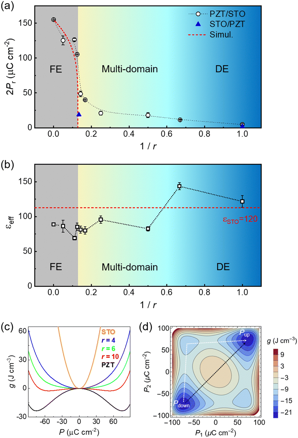 | ||
| Fig. 15 Characterization and modeling of PZT/STO stacks. (a) 2Prvs. 1/r for PZT/STO (open symbols) and STO/PZT (solid symbol) stacks. The dashed line is the simulation result using a single-domain model. (b) εeffvs. 1/r for PZT/STO stacks. The dashed line indicates the dielectric constant for single-layer STO. (c) Simulated g(P) for PZT/STO stacks with different r within the single-domain model. Adapted from ref. 39 with permission from American Physical Society, copyright 2021. (d) Simulated free energy contour plot of PZT hosting a DW as functions of P1 and P2. Reproduced from ref. 139 with permission. | ||
Under the single-domain conditions (D ≈ P and ∇P = 0), this model predicts a FE–DE transition at a critical thickness ratio rc = 7.8, where Pr vanishes (Fig. 15(a)) and the free energy evolves from a double-well to a single energy minimum at P = 0 (Fig. 15(c)). Even though the simulated rc agrees well with the experimental result (Fig. 15(a)), the residue hysteresis window and gradual decrease of Pr in PZT/STO stacks beyond rc cannot be captured by the single-domain model.39 The possible explanations include the contribution of STO, an incipient ferroelectric with nonzero Pr at high bias,82 and the emergence of a multidomain state between the FE and DE phases.19,138,140Fig. 15(d) shows the simulated energy profile of PZT hosting a 180° DW between two polar domains with independent polarizations of P1 and P2 based on eqn (2).139 Switching between the fully polarized single-domain states (two diagonal corners: P1 = P2 = ±Pr) can either go through the dielectric state (center point: P1 = P2 = 0) or detour to the off-diagonal local energy minima, which correspond to the multidomain state (both P1 and P2 are finite). For the PZT/STO stack, the off-diagonal points can evolve into global energy minimum in a certain range of r, preferring the multidomain state rather than the dielectric state. The slow DW motion during polarization switching results in residual Pr. This multidomain state can be suppressed by further reducing the ferroelectric content, and the PZT/STO stack eventually settles at a nonpolarized, dielectric state with entirely quenched Pr.
Hao et al. investigated the transient NC effect in the PZT/STO stacks.39 As shown in Fig. 16(a), when a square wave of source voltage (Vs) larger than the coercive voltage is applied to the PZT/STO stack with r = 8, the voltage across the capacitor (Vcap) exhibits a prominent damping during the initial charging (Fig. 16(a) and (b)), the characteristic behavior of the transient NC effect. In the Q–V curves deduced by integrating the charging current, an S-shape emerges (Fig. 16(c)), which is the direct manifestation of the NC mode (Fig. 15(c)). The voltage damping behavior and S-shape in Q–V gradually diminish with increasing STO content, becoming barely visible in the r = 6 sample (Fig. 16(c)), which is consistent with its vanishing ferroelectric order (Fig. 15(c)).
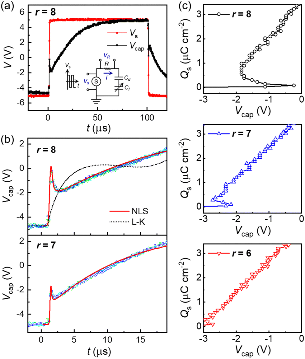 | ||
| Fig. 16 Transient NC effect in PZT/STO stack capacitors. (a) Voltage across a PZT/STO capacitor with r = 8 (Vcap) upon applied square wave source voltage (Vs). Inset: Schematic experimental setup. (b) Vcap(t) in the transient NC regime (open symbols) for the r = 8 and 7 samples with fits to the KAI/NLS model (solid line) and LK model (dotted line). (c) Qsvs. Vcap in PZT/STO stacks with r = 8, 7, and 6. Adapted from ref. 39 with permission from American Physical Society, copyright 2021. | ||
As shown in Fig. 16(b), the transient NC behavior in the PZT/STO stack cannot be described by the Landau–Khalatnikov (LK) dissipative model based on single-domain polarization switching.146 Instead, the nucleation-limited-switching (NLS) model can quantitatively describe the fast Vcap damping followed by slow recovery.146,147 Phenomenologically, this model considers polarization switching involving multiple independent nucleation sites, where the domain growth is constrained by defect pinning and grain size. The polarization switching within a single-domain region is characterized by the Kolmogorov–Avrami–Ishinashi (KAI) factor 1 − exp[−(t/t0)n], where t0 characterizes the time scale of DW propagation between different nucleation regions. Modeling the transient NC behavior using the KAI/NLS model reveals a narrow distribution of t0 for the r = 8 sample, consistent with the single-domain scenario, and a notably broader distribution of t0 for the r = 7 sample.39 The latter points to a multidomain state, where the DW motion is hindered by the formation of quasi-static, soft DWs, resulting in heterogeneous switching dynamics across different switching regions with a large variation in t0. The emergence of the multi-domain state can be utilized to anchor the steady-state NC effect, which is essential for the operation of NC-FETs, as illustrated in Section 5.1.3.
5. Ferroelectric oxide–2D van der Waals heterostructures
5.1 Ferroelectric field effect in van der Waals materials
Fig. 17(a) shows the longitudinal resistivity ρxxvs. Vg at 2 K taken on a 1L graphene FET back-gated by a BSTO thin film, which exhibits switching hysteresis that is consistent with ferroelectric polarization doping.149 The corresponding carrier density has been deduced from Hall measurements, n = 1/eRH, where RH is the Hall coefficient (Fig. 17(b)). Beyond the hysteresis window, BSTO behaves as a typical high-κ dielectric, with low temperature κ close to 100. Due to the efficient dielectric screening, the ferroelectric-gated graphene FETs exhibit high mobilities,49 with a field effect mobility of up to 23000 cm2 V−1 s−1 and nonvolatile modulation of the quantum Hall effect (Fig. 17(c) and (d)) observed in BSTO-gated 1L graphene.52,149
 | ||
| Fig. 17 Ferroelectric field effect in vdW FETs. (a)–(d) A 1L graphene FET with a BSTO back-gate. (a) ρxx(Vg) and (inset) σ vs. −n at 2 K. (b) 1/eRHvs. Vg at 2 K. Inset: ρxyvs. B at Vg = −1 V for up-sweep. Adapted from ref. 149 with permission from AIP Publishing, copyright 2022. (c) ρxx and (d) ρxyvs. Vg at 2 K and 9 T. Reproduced from ref. 52 with permission from American Chemical Society, copyright 2013. (e)–(g) A few-layer MoS2 FET with an SiO2 back-gate and a PZT membrane top-gate. (e) Device schematic. (f) Optical device image. (g) Idsvs. Vbg at 300 K for the no poling, Pup, and Pdown states of the PZT top-gate. (insets) PFM images of PZT (right) and device retention for the Pup and Pdown states of PZT (bottom). Adapted from ref. 28 with permission from American Chemical Society, copyright 2023. | ||
For 2D FETs back-gated by PZT and BSTO, the high temperature switching hysteresis is often opposite to that expected for ferroelectric polarization doping, known as an anti-hysteresis.50,52,53 When the van der Waals layer is transferred on the ferroelectric oxide at temperatures below TC, the bound charge on the ferroelectric surface is pre-screened by the ambient charged adsorbates50 or surface defect states,53 whose dynamic response to the applied electric field can over-screen the ferroelectric polarization and lead to the anti-hysteresis. To achieve appropriate switching hysteresis in 2D vdW FETs at room temperature, it is preferrable to exploit high-temperature transfer above TC53 or work with a top-gate geometry. In ref. 28, Wu et al. fabricated few-layer MoS2 FETs sandwiched between a SiO2 back-gate and a PZT membrane top-gate (Fig. 17(e) and (f)), using conductive AFM to switch PZT's polarization. These devices exhibit nonvolatile modulation of the source–drain current (Ids) that agrees with ferroelectric polarization switching, with a current on–off ratio of up to 2 × 10⁵ and no apparent decay for 3 days at 300 K (Fig. 17(g)).
The ferroelectric oxides possess high dielectric constants (Fig. 14(e)), resulting in soft remote surface optical (RSO) phonon modes that can significantly impact the mobility of the 2D channel.4,149–151Fig. 18(a) shows ρxx(T) at different carrier densities for a BSTO-gated 1L graphene FET.149 Beyond the electron–hole puddle region, ρxx decreases upon lowering temperature due to phonon scattering, which can be well described by:
 | (3) |
 | ||
| Fig. 18 Effect of RSO phonons on a BSTO-gated 1L graphene FET. (a) ρxx(T) at various hole doping levels with fits to eqn (3). (b) Mobility limit at 300 K imposed by the LA and four RSO phonon modes and the overall contribution (total). Reproduced from ref. 149 with permission from AIP Publishing, copyright 2022. | ||
 , with V0 the KP barrier, L the superlattice period, and vF = 108 cm s−1, the Fermi velocity of graphene).157 The dielectric thickness separating the gate electrode and graphene channel also leads to spatially dispersed potential profiles. In contrast, the ferroelectric domain approach can generate a step-like potential profile through direct contact with graphene, and the polarization doping of ferroelectric oxides such as PZT can be orders of magnitude higher than those of dielectric gates.
 | ||
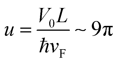
| Fig. 19 PZT induced 1D graphene superlattice. (a) Schematic Kronig–Penney potential. (b) Sample schematic. (c) and (d) Optical images of an h-BN/graphene/PZT sample before (c) and after (d) the deposition of the Au top-gate electrode. (e) R□(δn) for pristine graphene and a 1D GSL sample (L = 205 nm) in the Rxx configuration, with (f) Rxxvs. δn and B. (g) R□(δn) for a 1D GSL sample (L = 199 nm) in the Ryy configuration, with (h) Ryyvs. δn and B. The dashed lines illustrate the modeled Landau fans, with the filling factors labeled. (i) Calculated band structure for 1D GSL with scaled dimensionless KP potent u = 90π. (j) ΔnDPvs. L with a fit (dashed line) on linear and (inset) semi-log scales. Adapted from ref. 23 with permission from American Physical Society, copyright 2024. | ||
In ref. 23, Li et al. have achieved high KP potential (u ∼ 90π) in 1D GSL by fabricating graphene FETs sandwiched between an h-BN top-gate and a PZT back-gate with prepatterned stripe domains of period L = 200–300 nm (Fig. 19(b)–(d)).23 A polarization doping difference of up to 3 × 1013 cm−2 between the Pup and Pdown states has been induced in graphene at low temperatures due to the pyroelectric effect, corresponding to a high KP potential of 0.9 eV. For the 1D GSL with ŝ parallel to the current direction (denoted as Rxx), two satellite Dirac points emerge in R□vs. electron doping induced by the top-gate (δn) (Fig. 19(e)), indicating the formation of higher-order bands due to superlattice Brillouin zone folding. In magnetic fields, Rxx develops into three sets of Landau fans, originating from the original Dirac point and two satellite Dirac points (Fig. 19(f)). For the 1D GSL with ŝ perpendicular to the current direction (denoted as Ryy), R□(δn) exhibits a single peak (Fig. 19(g)) and only one set of Landau fans (Fig. 19(h)), confirming the highly anisotropic magnetotransport properties of the 1D GSL.
For V0 = 0.9 eV and L = 200 nm, the scaled dimensionless KP potential reaches u = 90π. The corresponding band structure exhibits a highly flattened band along ky (E = ±ħvF(kx + 2Nπ/L)) with strongly suppressed Fermi velocity vy ∼ 0.01 vF (Fig. 19(i)). Experimentally, the relation between the average carrier density interval between two consecutive Dirac points and the superlattice period can be described by: ΔnDP = ALβ, with β = −1.18 ± 0.06 (Fig. 19(j)). This quasi-inverse relation is a hallmark of the 1D GSL in the high KP potential limit, and the proportionality constant A = 2/a0 yields a0 = 2.40 Å, which is in excellent agreement with the graphene lattice constant 2.46 Å.
 , where Cch and Cg are the channel and gate capacitance, respectively. For a conventional dielectric gate with positive capacitance, the Boltzmann statistics impose a fundamental limit of SS ≈ 60 mV decade−1 at 300 K. It has been proposed that the effective negative capacitance in a ferroelectric gate close to P = 0 (Fig. 14(a)) can be exploited to achieve steep-slope switching, or sub-60 mV decade−1 SS at room temperature,141,142 which can lead to energy-efficient logic devices with reduced operation voltage. Previous studies of NC-FETs have focused on utilizing a ferroelectric/dielectric stack gate to stabilize the steady-state NC mode,7 and it is challenging to quench the ferroelectric hysteresis and achieve steep-slope switching at low gate-voltage. In ref. 55, Song et al. showed that it is possible to leverage the metastable polar state in ferroelectric DWs to enable steep-slope switching in a MoS2 based NC-FET at ultra-low Vg towards hysteresis-free operation. Fig. 20(a) shows the 300 K transfer curves (Idvs. Vg) of a few-layer (FL) MoS2 FET back-gated by polycrystalline PbZr0.35Ti0.65O3, which exhibits a current switching ratio of up to 8 × 10⁶ over a small gate window of Vg = ±0.5 V that is below the coercive voltage Vc. The SS is below the Boltzmann limit over three decades of Id for the forward Vg-sweep and over one decade of Id for the backward Vg-sweep. The minimum SS for this device is SSmin = 37 mV decade−1 and reaches SSmin = 9.7 mV decade−1 in a bilayer MoS2 FET at 300 K (Fig. 20(b)).
 | ||
| Fig. 20 DW enabled MoS2 NC-FET gated by polycrystalline PbZr0.35Ti0.65O3. (a) Idvs. Vg of a few-layer MoS2 FET at 300 K. Insets: Device schematic (top) and deduced SS vs. Id (bottom). (b) Idvs. Vg of a bilayer MoS2 FET at 300 K. Insets: AFM image of the device (top) and deduced SS vs. Id (bottom). (c) Average SS vs. T taken on 2 bilayer FETs and 3 FL FETs. The dashed lines in (a)–(c) indicate the Boltzmann limit. (d) Comparison of the room temperature current on/off ratio vs. operation voltage window ΔVg for various NC-FETs and FeFETs with MoS2 channels.158–168 (e) Force field simulation of a flux-closure type domain structure (left) and the change of local polarization upon small bias below Vc (right) in PZT. (f) L-PFM images of a domain structure on PZT with progressively higher DC Vbias, with the DW position highlighted. (g) Areal density of DW length lDW/A vs. Vbias extracted from (f) and SSavgvs. Vg-scan range taken on bilayer MoS2 FETs. Adapted from ref. 55 with permission from Springer Nature, copyright 2022. | ||
Compared with conventional NC-FETs, these MoS2-based NC-FETs exploit a single-layer polycrystalline PZT gate. The steep-slope switching and nearly hysteresis-free behavior at low Vg have been consistently observed in multiple bilayer and FL devices at different temperatures (Fig. 20(c)) and remain stable across different source–drain voltages and gate-voltage scan rates. The high Ion/Ioff achieved over a small operation voltage window of ΔVg = 0.75 V makes the device performance highly competitive compared with other MoS2-based NC-FETs and FE-FETs (Fig. 20(d)).158–168 This quasi-static NC mode has been attributed to the high density DWs in the polycrystalline PZT back-gate. Force field simulation shows that frustrated dipoles with flux-closure-type chiral rotation within the PZT DW can be polarized at an electric field well below Ec. It results in an abrupt jump in local polarization (Fig. 20(e)), which can quantitatively account for the steep-slope switching in surface MoS2 at Vg = −0.25 V. While the 180° DW in bulk PZT is known to be of Ising type with unit-cell-scale width,169 it has been shown that the flux-closure-type DW emerges in the presence of strong depolarization field, e.g., at the ferroelectric surfaces,170 grain boundaries,171 and ferroelectric/dielectric interfaces.19,20
The suppression of DW density at low bias voltage has been confirmed by PFM studies. Fig. 20(f) shows the lateral PFM (L-PFM) image of a polycrystalline PZT film, which hosts a high density of DWs at zero Vbias. The sample is subsequently imaged with progressively higher DC Vbias that is below Vc applied, which reveals a suppressed DW density with increasing Vbias. Studies of bilayer MoS2 NC-FETs show that the SSmin increases monotonically with increasing Vg-range (Fig. 20(g)), which correlates well with the reduced DW areal density, pointing to the critical role of the metastable polar state in the DW in stabilizing the NC effect.
5.2 Ferroelectric oxide interfaced with polar 2D materials
 | ||
| Fig. 21 Characterization of the PZT/1L MoS2 heterostructure. (a) Schematic experimental setup. (b) PFM phase images of 1L MoS2 transferred on a 50 nm PZT film prepatterned with square domains. (c) Room temperature PL spectra of 1L MoS2 on the Pup and Pdown domains shown in (b). Inset: PL mapping of the peak intensity (upper), width (middle), and position (lower) of 1L MoS2 on Pup and Pdown domains of PZT, with DW positions marked. (d) Fits to the PL spectra revealing the modulation of neutral excitons (A0) and negative trions (A−). Adapted from ref. 24 with permission from Springer Nature, copyright 2020. | ||
Fig. 21(b)–(d) shows a 1L MoS2 flake transferred on a 50 nm PZT film pre-patterned with square domains, which reveals nonvolatile tuning of the PL signal. The intensity areal ratio between the negative trions (A−) and neutral excitons (A0), extracted by fitting the PL spectra (Fig. 21(d)), suggests that the induced doping is dominated by the interfacial screening charge rather than ferroelectric polarization.24 For (001) PZT thin films, normal-incidence light yields prominent SHG signals at the DW regions (Fig. 22(a)).24 The light polarization of the SHG signal is perpendicular to the DW, which points to the presence of in-plane polarization at the Néel-type DWs, consistent with previous reports.174,175 For 1L MoS2/PZT heterostructures, there is a strong filtering effect of the SHG signal that depends on the relative alignment of polar axes as well as the measurement geometry.
 | ||
| Fig. 22 DW filtering of SHG signals at 1L MoS2/PZT interfaces. (a) R-SHG mapping of a domain structure on PZT with no analyzer applied before (a) and after (b) the transfer of 1L MoS2 on top. (c) Schematic of a flux-closure type polar rotation at the surface of a 180° DW. (d) Schematic of the polar alignment at a 1L MoS2/PZT interface. The arrows mark the local polarization directions. Reproduced from ref. 24 with permission from Springer Nature, copyright 2020. (e) PFM phase image and (f) R-SHG mapping of a hexagonal domain on bare PZT, and (g) R-SHG mapping after a 1L MoS2 transferred on top. The open arrows show the direction of the incident light polarization. The dashed (solid) arrows mark the polarization directions of the DWs (MoS2). (h) Polar plots of normalized R-SHG intensity vs. ϕ taken at different DWs in (g) with fits to nonlinear electromagnetic theory (dashed lines). Reproduced from ref. 25 with permission from Wiley-VCH GmbH, copyright 2022. | ||
Fig. 22(b) shows the SHG mapping of a 1L MoS2/PZT heterostructure, where one of the polar axes of MoS2 is aligned with the vertical DWs. In the reflected mode (R-SHG), the SHG signal is modulated at the DWs, remaining unchanged at the polar domains. The SHG signal on the horizental DWs shows alternating enhancement and suppression in intensity, which reflects the alignment between the polar axis of MoS2 and the in-plane polarization of DW. DFT calculation shows that the in-plane polarization of a flux-closure type DW in PZT (Fig. 22(c)) is comparable with that of 1L MoS2.24 Combining these two can lead to about four times of the SHG intensity when the two polar axes are aligned and close to zero SHG intensity when they are anti-aligned (Fig. 22(d)).24 The SHG signal on the the vertical DWs, on the other hand, cannot be differentiated from the background MoS2, as the two polar axes are orthogonal to each other. The 1L MoS2 can thus serve as an atomic-scale polarizer that can modulate the strength of the SHG signal based on its polar alignment with the DW. The modulation of the SHG strength and polarization can be quantitatively modeled using the nonlinear electromagnetic theory considering the coupling of second-order nonlinear optical susceptibility tensors for MoS2 and PZT DW. As shown in Fig. 22(e)–(h), both the amplitude and polarization of the SHG signal can be tuned by varying the angle between the polar axes of MoS2 and PZT DW, which have been well captured by theoretical modeling.25
In the transmitted mode (T-SHG) for 1L MoS2 on top of PZT thin films (MoS2/PZT), the polar domain also exerts a strong tuning effect on the SHG signal (Fig. 23(a)). A similar effect has been observed in R-SHG for reversed sample geometry (PZT/MoS2), i.e., with 1L MoS2 underneath a PZT membrane (Fig. 23(b)). The coupling with the PZT polar domain leads to three-fold polarization of the SHG signal, or C3v symmetry, with the intensity peaking along the zig-zag directions of MoS2 (Fig. 23(c)–(h)). This is in sharp contrast to the C6h symmetry observed in standalone MoS2176 and C2v symmetry observed in R-SHG of 1L MoS2/PZT heterostructures (Fig. 22(h)), which can be well explained by considering the coupling of second-order nonlinear optical susceptibility tensors for MoS2 and PZT (Fig. 23(e) and (h)).25 For the PZT/MoS2 geometry, the domain structure in the top PZT membrane is reconfigurable, facilitating in operando device operation.
 | ||
| Fig. 23 Ferroelectric domain control of SHG signals. (a) Schematic of a 1L MoS2/PZT thin film. (b) Schematic of PZT membrane/1L MoS2. (c)–(e) T-SHG studies of MoS2/PZT. (c) PFM phase image and (d) T-SHG mapping of a domain structure on MoS2/PZT. The excitation laser power is 30 mW. (e) Polar plots of normalized T-SHG intensity vs. ϕ taken on the Pup and Pdown domains in (d) with fits (solid lines). (f)–(h) R-SHG studies of PZT membrane/MoS2. (f) PFM phase image and (g) R-SHG mapping of a domain structure on PZT/MoS2. The excitation laser power is 7 mW. (h) Polar plots of normalized R-SHG intensity vs. ϕ taken on the Pup and Pdown domains in (g) with fits (solid lines). Reproduced from ref. 25 with permission from Wiley-VCH GmbH, copyright 2022. | ||
 | ||
| Fig. 24 Enhanced polar alignment in thin CIPS on PZT. (a) Sample schematic. (b) PFM phase images of 13–14 nm CIPS flakes transferred on PZT, Si, and Au base layers. (c) PFM phase and (inset) AFM topography images of CIPS flakes with various thickness transferred on a prepatterned domain structure on PZT. (d) Averaged d33 for 14 nm CIPS on Au, Si, and PZT. (e) dCIPS33 of CIPS on PZT as a function of flake thickness. Adapted from ref. 22 with permission from American Chemical Society, copyright 2023. | ||
The enhanced polar alignment and dCIPS33 in ultrathin CIPS flakes point to the interfacial coupling with the PZT underneath. The sign change of dCIPS33 further suggests that the sample is settled at the metastable state (MS) rather than the ground state (GS) of the quadruple energy well (Fig. 25(a) and (b)).178 DFT calculations of the CIPS/PbTiO3 heterointerface reveal a strain-induced lattice distortion in the interfacial CIPS layer, which results in a tilted free-energy profile that favors the anti-alignment between the polarization of CIPS and PbTiO3 and settles at the metastable state (Fig. 25(b)).
 | ||
| Fig. 25 Interface tuning of ferroelectricity in CIPS via PZT. (a) and (b) Schematics of sulfur and copper ion arrangements (upper panels) and ferroelectric quadruple-well energy profiles (lower panels) for standalone CIPS (a) and CIPS on PbTiO3 with polarization antialigned (b). (c) In situ PFM images at selected temperatures taken on 13 nm and 55 nm CIPS on PZT, corresponding to the red boxed areas in Fig. 24(c). (d) Monte Carlo simulations of the mean Cu position at different temperatures. Reproduced from ref. 22 with permission from American Chemical Society, copyright 2023. | ||
The titled free energy well further enhances the ferroelectric ordering energy. Fig. 25(c) shows the in situ PFM images of CIPS on PZT at elevated temperatures. For the 55 nm flakes, the domain structure becomes blurred at 100 °C, suggesting that it is above TC, which is consistent with the bulk value (TC ∼ 42 °C).179 For the 13 nm CIPS, TC is substantially enhanced to above 200 °C. Monte Carlo simulations based on atomic positions of CIPS strained on PbTiO3 predict a 63% increase of TC compared with that of standalone CIPS (Fig. 25(d)), which is in excellent agreement with the experimental results.22 The enhanced polarization and TC for thin CIPS on PZT, as well as their anti-aligned polarization, have been confirmed via in situ, temperature-dependent PL studies, which reveal an interface-strain induced lattice change in CIPS.183 A similar enhancement of polar domain formation and the piezoelectric coefficient has been observed in the organolead trihalide perovskite CH3NH3PbI3 interfaced with PZT,21 which has been attributed to the over-screened ferroelectric polarization induced dipole field that promotes the polar alignment in a polar liquid state of the hybrid perovskite.184
6. Conclusions and perspectives
In this feature article, we use ferroelectric perovskite oxide-based heterostructures as model systems to illustrate various emergent phenomena mediated by interfacial coupling of charge, lattice, and polar symmetry. The discussion centers on epitaxial complex oxide heterostructures and ferroelectric thin films and membranes interfaced with 2D van der Waals materials. The electrostatic and mechanical boundary conditions have profound impacts on the polar properties of ferroelectric oxide thin films, leading to large variations in the ferroelectric Curie temperature and coercive field. The TC of epitaxial ferroelectric films can be over 300 °C higher than the bulk value due to compressive strain. It is interesting to note that the strain level can be sustained in suspended oxide membranes after being transferred on a different base layer, and the properties of the base layer (e.g., surface roughness and bonding type) can affect the level of strain relaxation. The DW roughness and its thermal evolution have been systematically analyzed, which reveal the critical role of the base layer and the complex interplay of interfacial screening capacity, atomic bonding, surface morphology, and defect migration in determining the static distribution and dynamic response of the DW. The effect of the depolarization field is manifested in the ferroelectric–dielectric transition, transient negative capacitance mode, and domain formation in ferroelectric/dielectric heterostructures. The gained information is critical for understanding the polarization switching dynamics, domain size limit, and thermal stability and can facilitate the development of domain/DW-based memory and logic devices with high density, high speed, low power, and high operation temperature.We also survey the coupling mechanisms and emergent functionalities of ferroelectric oxide-based heterointerfaces, including the ferroelectric field effect control of the electronic and magnetic states in correlated oxides and quantum transport in graphene, as well as the filtering effect of nonlinear optical response of MoS2via ferroelectric polarization and DWs. Nanoscale domain patterning further allows the design of 1D graphene superlattices and programmable second harmonic generation in ferroelectric/MoS2 heterostructures. The interfacial strain coupling with ferroelectric thin films have been leveraged to enhance the polar alignment, piezoelectric response, and TC in ultrathin 2D ferroelectric CIPS flakes. Various emerging device concepts have been discussed, including Mott FeFETs, ferroelectric tunnel junctions, steep slope NC FETs, electron lensing devices, and in operando nonlinear optical filters, highlighting their application potential in high performance, reconfigurable nanoelectronics, optoelectronics, and nano-photonics.
Our discussions showcase the rich functionalities and high application potential of ferroelectric perovskite oxide-based heterostructures. Looking forward, we outline several potential research directions that can broaden the research portfolio based on functional design of ferroelectric oxide heterostructures.
Novel materials synthesis
For technological applications of ferroelectric oxide-gated 2D vdW FETs, it is essential to develop a scalable synthesis method and CMOS-compatible device architectures. In previous studies of 2D FeFETs, ferroelectric oxides are mainly adopted as a global back-gate.4 Converting to a top-gate device structure involves dry-transfer of ferroelectric membranes,28 which requires multiple fabrication steps and is not scalable. The recently developed remote epitaxy technique builds on MBE and laser MBE growth of complex oxide thin films (e.g., SrTiO3185 and BaTiO3186) on substrates buffered with porous graphene, which can be extended to other vdW buffer materials for achieving multifunctional ferroelectric heterointerfaces.Oxide moiré engineering29,187 based on stacking and twisting oxide membranes has attracted enormous research interest as it provides a new material platform for exploring functionalities not expected in the single-phase nano-materials, as demonstrated in the van der Waals moiré systems.188 Unlike the van der Waals materials, which are layered by nature, the transition metal oxides are based on semi-ionic/semi-covalent bonds. This attribute both imposes challenges in materials processing, e.g., for stabilizing small twisting angle phases that are thermodynamically highly unstable, and offers new opportunities capitalizing on the stronger interface interaction and potential modulation for band reconstruction. Experimentally, novel 2D polar vortex patterns have been observed in twisted BaTiO3.29 It is further conceivable to design novel polar states and magnetism in twisted oxides that are neither polar nor magnetic. The appearance of vortex–antivortex polarization and doping-induced unconventional d0 magnetism has been theoretically predicted in twisted SrTiO3 bilayers,189 making it promising for realizing a multiferroic state that is controllable via the electric field effect.
Incorporation of binary ferroelectric oxides
Binary ferroelectric oxides such as doped HfO2 and ZrO2 are compatible with the mainstream CMOS processing and have high potential for industrial applications.190 Single crystalline doped HfO2 has been recently demonstrated,191 and it offers the opportunity to investigate ferroelectricity from a new material perspective. Specifically, this class of ferroelectrics exhibit high sensitivity to surface chemistry,192,193 possess scale-free DWs,194 and are potentially immune to the depolarization effect.195 It is of both fundamental and technological interest to construct HfO2-based heterostructures and understand how the interfacial electrode would affect the ferroelectric order parameter, polarization switching dynamics, and DW configurations.Theory-driven material discovery and functionality design
The rapid development of DFT-based computational material search, especially enabled by machine-learning, offers unforeseeable research opportunities to design novel ferroelectric oxides and heterostructures with tailored functionalities. One direction of interest is to design ferroelectric oxide with non-trivial topology properties. It has been theoretically shown that noncentrosymmetric BiInO3 is ferroelectric and can host persistent spin texture, a momentum-independent spin configuration that can be coupled with the ferroelectric polarization,196 while the polar phase BiInO3 remains to be realized experimentally.197,198 Also of interest is to impose polar symmetry and modulate the electronic and magnetic states in perovskites by designing the oxygen octahedral rotation through epitaxial strain and superlattice engineering.199,200 This approach has been adopted to stabilize a BiFeO3-like structure201 and anchor room temperature ferroelectricity in CaTiO3.34Data availability
There are no new data generated in this work.Conflicts of interest
The authors have no conflicts to disclose.Acknowledgements
This work is supported by the National Science Foundation through EPSCoR RII Track-1: Emergent Quantum Materials and Technologies (EQUATE), award no. OIA-2044049 and DMREF award no. DMR-2118828, the UNL Grand Challenges catalyst award entitled Quantum Approaches addressing Global Threats, and the Nebraska Center for Energy Sciences Research.References
- M. Dawber, K. M. Rabe and J. F. Scott, Physics of thin-film ferroelectric oxides, Rev. Mod. Phys., 2005, 77, 1083–1130 CrossRef CAS
.
- N. Setter, D. Damjanovic, L. Eng, G. Fox, S. Gevorgian, S. Hong, A. Kingon, H. Kohlstedt, N. Y. Park, G. B. Stephenson, I. Stolitchnov, A. K. Tagantsev, D. V. Taylor, T. Yamada and S. Streiffer, Ferroelectric thin films: Review of materials, properties, and applications, J. Appl. Phys., 2006, 100, 051606 CrossRef
- L. W. Martin and A. M. Rappe, Thin-film ferroelectric materials and their applications, Nat. Rev. Mater., 2017, 2, 16087 CrossRef CAS
- X. Hong, Emerging ferroelectric transistors with nanoscale channel materials: the possibilities, the limitations, J. Phys.: Condens. Matter, 2016, 28, 103003 CrossRef PubMed
- M. Bibes, J. Villegas and A. Barthelemy, Ultrathin oxide films and interfaces for electronics and spintronics, Adv. Phys., 2011, 60, 5–84 CrossRef CAS
- S. Oh, H. Hwang and I. K. Yoo, Ferroelectric materials for neuromorphic computing, APL Mater., 2019, 7, 091109 CrossRef
- M. A. Alam, M. W. Si and P. D. D. Ye, A critical review of recent progress on negative capacitance field-effect transistors, Appl. Phys. Lett., 2019, 114, 090401 CrossRef
- N. Sezer and M. Koç, A comprehensive review on the state-of-the-art of piezoelectric energy harvesting, Nano Energy, 2021, 80, 105567 CrossRef CAS
- Y. Zhang, W. Jie, P. Chen, W. Liu and J. Hao, Ferroelectric and Piezoelectric Effects on the Optical Process in Advanced Materials and Devices, Adv. Mater., 2018, 30, 1707007 CrossRef PubMed
- C. H. Ahn, J. M. Triscone and J. Mannhart, Electric field effect in correlated oxide systems, Nature, 2003, 424, 1015–1018 CrossRef CAS PubMed
- C. H. Ahn, A. Bhattacharya, M. Di Ventra, J. N. Eckstein, C. D. Frisbie, M. E. Gershenson, A. M. Goldman, I. H. Inoue, J. Mannhart, A. J. Millis, A. F. Morpurgo, D. Natelson and J. M. Triscone, Electrostatic modification of novel materials, Rev. Mod. Phys., 2006, 78, 1185–1212 CrossRef CAS
- C. A. F. Vaz, J. Hoffman, C. H. Ahn and R. Ramesh, Magnetoelectric Coupling Effects in Multiferroic Complex Oxide Composite Structures, Adv. Mater., 2010, 22, 2900–2918 CrossRef CAS PubMed
- C. A. F. Vaz, Y. J. Shin, M. Bibes, K. M. Rabe, F. J. Walker and C. H. Ahn, Epitaxial ferroelectric interfacial devices, Appl. Phys. Rev., 2021, 8, 041308 CAS
- H. Ryu, K. Xu, D. Li, X. Hong and W. Zhu, Empowering 2D nanoelectronics via ferroelectricity, Appl. Phys. Lett., 2020, 117, 080503 CrossRef CAS
- X. Hong, A. Posadas, A. Lin and C. H. Ahn, Ferroelectric-field-induced tuning of magnetism in the colossal magnetoresistive oxide La1−xSrxMnO3, Phys. Rev. B: Condens. Matter Mater. Phys., 2003, 68, 134415 CrossRef
- X. Hong, A. Posadas and C. H. Ahn, Examining the screening limit of field effect devices via the metal–insulator transition, Appl. Phys. Lett., 2005, 86, 142501 CrossRef
- A. K. Yadav, C. T. Nelson, S. L. Hsu, Z. Hong, J. D. Clarkson, C. M. Schlepuetz, A. R. Damodaran, P. Shafer, E. Arenholz, L. R. Dedon, D. Chen, A. Vishwanath, A. M. Minor, L. Q. Chen, J. F. Scott, L. W. Martin and R. Ramesh, Observation
of polar vortices in oxide superlattices, Nature, 2016, 530, 198 CrossRef CAS PubMed
- Z. Hong, A. R. Damodaran, F. Xue, S.-L. Hsu, J. Britson, A. K. Yadav, C. T. Nelson, J.-J. Wang, J. F. Scott, L. W. Martin, R. Ramesh and L.-Q. Chen, Stability of Polar Vortex Lattice in Ferroelectric Superlattices, Nano Lett., 2017, 17, 2246–2252 CrossRef CAS PubMed
- P. Zubko, J. C. Wojdel, M. Hadjimichael, S. Fernandez-Pena, A. Sene, I. Luk'yanchuk, J. M. Triscone and J. Iniguez, Negative capacitance in multidomain ferroelectric superlattices, Nature, 2016, 534, 524 CrossRef CAS PubMed
- A. K. Yadav, K. X. Nguyen, Z. J. Hong, P. Garcia-Fernandez, P. Aguado-Puente, C. T. Nelson, S. Das, B. Prasad, D. Kwon, S. Cheema, A. I. Khan, C. M. Hu, J. Iniguez, J. Junquera, L. Q. Chen, D. A. Muller, R. Ramesh and S. Salahuddin, Spatially resolved steady-state negative capacitance, Nature, 2019, 565, 468 CrossRef CAS PubMed
- J. Song, Z. Xiao, B. Chen, S. Prockish, X. Chen, A. Rajapitamahuni, L. Zhang, J. Huang and X. Hong, Enhanced Piezoelectric Response in Hybrid Lead Halide Perovskite Thin Films via Interfacing with Ferroelectric PbZr0.2Ti0.8O3, ACS Appl. Mater. Interfaces, 2018, 10, 19218–19225 CrossRef CAS PubMed
- K. Wang, D. Li, J. Wang, Y. Hao, H. Anderson, L. Yang and X. Hong, Interface-Tuning of Ferroelectricity and Quadruple-Well State in CuInP2S6via Ferroelectric Oxide, ACS Nano, 2023, 17, 15787–15795 CrossRef CAS PubMed
- T. Li, H. Chen, K. Wang, Y. Hao, L. Zhang, K. Watanabe, T. Taniguchi and X. Hong, Transport Anisotropy in One-Dimensional Graphene Superlattice in the High Kronig-Penney Potential Limit, Phys. Rev. Lett., 2024, 132, 056204 CrossRef CAS PubMed
- D. Li, X. Huang, Z. Xiao, H. Chen, L. Zhang, Y. Hao, J. Song, D.-F. Shao, E. Y. Tsymbal, Y. Lu and X. Hong, Polar coupling enabled nonlinear optical filtering at MoS2/ferroelectric heterointerfaces, Nat. Commun., 2020, 11, 1422 CrossRef CAS PubMed
- D. Li, X. Huang, Q. Wu, L. Zhang, Y. Lu and X. Hong, Ferroelectric Domain Control of Nonlinear Light Polarization in MoS2via PbZr0.2Ti0.8O3 Thin Films and Free-Standing Membranes, Adv. Mater., 2023, 35, 2208825 CrossRef CAS PubMed
- S. R. Bakaul, J. Kim, S. Hong, M. J. Cherukara, T. Zhou, L. Stan, C. R. Serrao, S. Salahuddin, A. K. Petford-Long, D. D. Fong and M. V. Holt, Ferroelectric Domain Wall Motion in Freestanding Single-Crystal Complex Oxide Thin Film, Adv. Mater., 2020, 32, 1907036 CrossRef CAS PubMed
- S. R. Bakaul, S. Prokhorenko, Q. Zhang, Y. Nahas, Y. S. Hu, A. Petford-Long, L. Bellaiche and N. Valanoor, Freestanding Ferroelectric Bubble Domains, Adv. Mater., 2021, 33, 2105432 CrossRef CAS PubMed
- Q. Wu, K. Wang, A. Simpson, Y. Hao, J. Wang, D. Li and X. Hong, Electrode Effect on Ferroelectricity in Free-Standing Membranes of PbZr0.2Ti0.8O3, ACS Nanosci. Au, 2023, 3, 482–490 CrossRef CAS PubMed
- G. Sánchez-Santolino, V. Rouco, S. Puebla, H. Aramberri, V. Zamora, M. Cabero, F. A. Cuellar, C. Munuera, F. Mompean, M. Garcia-Hernandez, A. Castellanos-Gomez, J. Iñiguez, C. Leon and J. Santamaria, A 2D ferroelectric vortex pattern in twisted BaTiO3 freestanding layers, Nature, 2024, 626, 529 CrossRef PubMed
- A. Lin, X. Hong, V. Wood, A. A. Verevkin, C. H. Ahn, R. A. McKee, F. J. Walker and E. D. Specht, Epitaxial growth of Pb(Zr0.2Ti0.8)O3 on Si and its nanoscale piezoelectric properties, Appl. Phys. Lett., 2001, 78, 2034–2036 CrossRef CAS
- C. Dubourdieu, J. Bruley, T. M. Arruda, A. Posadas, J. Jordan-Sweet, M. M. Frank, E. Cartier, D. J. Frank, S. V. Kalinin, A. A. Demkov and V. Narayanan, Switching of ferroelectric polarization in epitaxial BaTiO3 films on silicon without a conducting bottom electrode, Nat. Nanotechnol., 2013, 8, 748–754 CrossRef CAS PubMed
- R. M. Moghadam, Z. Xiao, K. Ahmadi-Majlan, E. D. Grimley, M. Bowden, P.-V. Ong, S. A. Chambers, J. M. Lebeau, X. Hong, P. V. Sushko and J. H. Ngai, An Ultrathin Single Crystalline Relaxor Ferroelectric Integrated on a High Mobility Semiconductor, Nano Lett., 2017, 17, 6248–6257 CrossRef CAS PubMed
- A. R. Damodaran, J. C. Agar, S. Pandya, Z. H. Chen, L. Dedon, R. J. Xu, B. Apgar, S. Saremi and L. W. Martin, New modalities of strain-control of ferroelectric thin films, J. Phys.: Condens. Matter, 2016, 28, 263001 CrossRef PubMed
- J. R. Kim, J. Jang, K.-J. Go, S. Y. Park, C. J. Roh, J. Bonini, J. Kim, H. G. Lee, K. M. Rabe, J. S. Lee, S.-Y. Choi, T. W. Noh and D. Lee, Stabilizing hidden room-temperature ferroelectricity via a metastable atomic distortion pattern, Nat. Commun., 2020, 11, 4944 CrossRef CAS PubMed
- S. A. Chambers, Epitaxial growth and properties of doped transition metal and complex oxide films, Adv. Mater., 2010, 22, 219–248 CrossRef CAS PubMed
- K. R. Talley, C. L. Perkins, D. R. Diercks, G. L. Brennecka and A. Zakutayev, Synthesis of LaWN3 nitride perovskite with polar symmetry, Science, 2021, 374, 1488–1491 CrossRef CAS PubMed
- X. Hong, Nitride perovskite becomes polar, Science, 2021, 374, 1445–1446 CrossRef CAS PubMed
- J. P. Podkaminer, J. J. Patzner, B. A. Davidson and C. B. Eom, Real-time and in situ monitoring of sputter deposition with RHEED for atomic layer controlled growth, APL Mater., 2016, 4, 086111 CrossRef
- Y. Hao, T. Li, Y. Yun, X. Li, X. Chen, J. Song, Z. Ahmadi, J. E. Shield, X. Xu and X. Hong, Tuning Negative Capacitance in PbZr0.2Ti0.8O3/SrTiO3 Heterostructures via Layer Thickness Ratio, Phys. Rev. Appl., 2021, 16, 034004 CrossRef CAS
- X. Chen, X. Zhang, M. A. Koten, H. Chen, Z. Xiao, L. Zhang, J. E. Shield, P. A. Dowben and X. Hong, Interfacial Charge Engineering in Ferroelectric-Controlled Mott Transistors, Adv. Mater., 2017, 29, 1701385 CrossRef PubMed
- Y. Hao, X. Chen, L. Zhang, M.-G. Han, W. Wang, Y.-W. Fang, H. Chen, Y. Zhu and X. Hong, Record high room temperature resistance switching in ferroelectric-gated Mott transistors unlocked by interfacial charge engineering, Nat. Commun., 2023, 14, 8247 CrossRef CAS PubMed
- D. Lu, D. J. Baek, S. S. Hong, L. F. Kourkoutis, Y. Hikita and H. Y. Hwang, Synthesis of freestanding single-crystal perovskite films and heterostructures by etching of sacrificial water-soluble layers, Nat. Mater., 2016, 15, 1255–1260 CrossRef CAS PubMed
- D. Pesquera, A. Fernandez, E. Khestanova and L. W. Martin, Freestanding complex-oxide membranes, J. Phys.: Condens. Matter, 2022, 34, 383001 CrossRef CAS PubMed
- S. Puebla, T. Pucher, V. Rouco, G. Sanchez-Santolino, Y. Xie, V. Zamora, F. A. Cuellar, F. J. Mompean, C. Leon, J. O. Island, M. Garcia-Hernandez, J. Santamaria, C. Munuera and A. Castellanos-Gomez, Combining Freestanding Ferroelectric Perovskite Oxides with Two-Dimensional Semiconductors for High Performance Transistors, Nano Lett., 2022, 22, 7457–7466 CrossRef CAS PubMed
- J. Choi, K. J. Crust, L. Z. Li, K. Lee, J. L. Luo, J. P. So, K. Watanabe, T. Taniguchi, H. Y. Hwang, K. F. Mak, J. Shan and G. D. Fuchs, Tuning Exciton Emission via Ferroelectric Polarization at a Heterogeneous Interface between a Monolayer Transition Metal Dichalcogenide and a Perovskite Oxide Membrane, Nano Lett., 2024, 24, 8948–8955 CrossRef CAS PubMed
- T. Pucher, S. Puebla, V. Zamora, E. S. Viso, V. Rouco, C. Leon, M. Garcia-Hernandez, J. Santamaria, C. Munuera and A. Castellanos-Gomez, Strong Electrostatic Control of Excitonic Features in MoS2 by a Free-Standing Ultrahigh-κ Ferroelectric Perovskite, Adv. Funct. Mater., 2024, 34, 2409447 CrossRef CAS
- H. G. Wang, V. Harbola, Y. J. Wu, P. A. van Aken and J. Mannhart, Interface Design beyond Epitaxy: Oxide Heterostructures Comprising Symmetry-Forbidden Interfaces, Adv. Mater., 2024, 36, 202405065 Search PubMed
- K. Wang, Y. Hao, L. Zhang, Y. Zhang, X. Chen and X. Hong, Effect of correlated oxide electrodes on disorder pinning and thermal roughening of ferroelectric domain walls in epitaxial PbZr0.2Ti0.8O3 thin films, Phys. Rev. Mater., 2021, 5, 074402 CrossRef CAS
- X. Hong, A. Posadas, K. Zou, C. H. Ahn and J. Zhu, High-Mobility Few-Layer Graphene Field Effect Transistors Fabricated on Epitaxial Ferroelectric Gate Oxides, Phys. Rev. Lett., 2009, 102, 136808 CrossRef CAS PubMed
- X. Hong, J. Hoffman, A. Posadas, K. Zou, C. H. Ahn and J. Zhu, Unusual resistance hysteresis in n-layer graphene field effect transistors fabricated on ferroelectric Pb(Zr0.2Ti0.8)O3, Appl. Phys. Lett., 2010, 97, 033114 CrossRef
- C. Baeumer, S. P. Rogers, R. J. Xu, L. W. Martin and M. Shim, Tunable Carrier Type and Density in Graphene/PbZr0.2Ti0.8O3 Hybrid Structures through Ferroelectric Switching, Nano Lett., 2013, 13, 1693–1698 CrossRef CAS PubMed
- A. Rajapitamahuni, J. Hoffman, C. H. Ahn and X. Hong, Examining Graphene Field Effect Sensors for Ferroelectric Thin Film Studies, Nano Lett., 2013, 13, 4374–4379 CrossRef CAS PubMed
- M. H. Yusuf, B. Nielsen, M. Dawber and X. Du, Extrinsic and Intrinsic Charge Trapping at the Graphene/Ferroelectric Interface, Nano Lett., 2014, 14, 5437–5444 CrossRef CAS PubMed
- A. Lipatov, P. Sharma, A. Gruverman and A. Sinitskii, Optoelectrical Molybdenum Disulfide (MoS2)—Ferroelectric Memories, ACS Nano, 2015, 9, 8089–8098 CrossRef CAS PubMed
- J. Song, Y. Qi, Z. Xiao, K. Wang, D. Li, S.-H. Kim, A. I. Kingon, A. M. Rappe and X. Hong, Domain wall enabled steep slope switching in MoS2 transistors towards hysteresis-free operation, npj 2D Mater. Appl., 2022, 6, 77 CrossRef CAS
- E. B. Song, B. Lian, S. M. Kim, S. Lee, T. K. Chung, M. S. Wang, C. F. Zeng, G. Y. Xu, K. Wong, Y. Zhou, H. I. Rasool, D. H. Seo, H. J. Chung, J. Heo, S. Seo and K. L. Wang, Robust bi-stable memory operation in single-layer graphene ferroelectric memory, Appl. Phys. Lett., 2011, 99, 042109 CrossRef
- C. Baeumer, D. Saldana-Greco, J. M. P. Martirez, A. M. Rappe, M. Shim and L. W. Martin, Ferroelectrically driven spatial carrier density modulation in graphene, Nat. Commun., 2015, 6, 6136 CrossRef CAS PubMed
- A. Nguyen, P. Sharma, T. Scott, E. Preciado, V. Klee, D. Sun, I. H. D. Lu, D. Barroso, S. Kim, V. Y. Shur, A. R. Akhmatkhanov, A. Gruverman, L. Bartels and P. A. Dowben, Toward Ferroelectric Control of Monolayer MoS2, Nano Lett., 2015, 15, 3364–3369 CrossRef CAS PubMed
- F. Lo Presti, A. L. Pellegrino and G. Malandrino, Metal–Organic Chemical Vapor Deposition of Oxide Perovskite Films: A Facile Route to Complex Functional Systems, Adv. Mater. Interfaces, 2022, 9, 2102501 CrossRef CAS
- S. Liu, D. Zou, X. Yu, Z. Wang and Z. Yang, Transfer-Free PZT Thin Films for Flexible Nanogenerators Derived from a Single-Step Modified Sol–Gel Process on 2D Mica, ACS Appl. Mater. Interfaces, 2020, 12, 54991–54999 CrossRef CAS PubMed
- K. S. Novoselov, A. K. Geim, S. V. Morozov, D. Jiang, Y. Zhang, S. V. Dubonos, I. V. Grigorieva and A. A. Firsov, Electric Field Effect in Atomically Thin Carbon Films, Science, 2004, 306, 666–669 CrossRef CAS PubMed
- Y. Huang, E. Sutter, N. N. Shi, J. Zheng, T. Yang, D. Englund, H.-J. Gao and P. Sutter, Reliable Exfoliation of Large-Area High-Quality Flakes of Graphene and Other Two-Dimensional Materials, ACS Nano, 2015, 9, 10612–10620 CrossRef CAS PubMed
- Y. Huang, Y.-H. Pan, R. Yang, L.-H. Bao, L. Meng, H.-L. Luo, Y.-Q. Cai, G.-D. Liu, W.-J. Zhao, Z. Zhou, L.-M. Wu, Z.-L. Zhu, M. Huang, L.-W. Liu, L. Liu, P. Cheng, K.-H. Wu, S.-B. Tian, C.-Z. Gu, Y.-G. Shi, Y.-F. Guo, Z. G. Cheng, J.-P. Hu, L. Zhao, G.-H. Yang, E. Sutter, P. Sutter, Y.-L. Wang, W. Ji, X.-J. Zhou and H.-J. Gao, Universal mechanical exfoliation of large-area 2D crystals, Nat. Commun., 2020, 11, 2453 CrossRef CAS PubMed
- M. Velický, G. E. Donnelly, W. R. Hendren, S. McFarland, D. Scullion, W. J. I. DeBenedetti, G. C. Correa, Y. Han, A. J. Wain, M. A. Hines, D. A. Muller, K. S. Novoselov, H. D. Abruña, R. M. Bowman, E. J. G. Santos and F. Huang, Mechanism of Gold-Assisted Exfoliation of Centimeter-Sized Transition-Metal Dichalcogenide Monolayers, ACS Nano, 2018, 12, 10463–10472 CrossRef PubMed
- Y. Wu, I. Abdelwahab, K. C. Kwon, I. Verzhbitskiy, L. Wang, W. H. Liew, K. Yao, G. Eda, K. P. Loh, L. Shen and S. Y. Quek, Data-driven discovery of high performance layered van der Waals piezoelectric
NbOI2, Nat. Commun., 2022, 13, 1884 CrossRef CAS PubMed
- A. Castellanos-Gomez, M. Buscema, R. Molenaar, V. Singh, L. Janssen, H. S. J. van der Zant and G. A. Steele, Deterministic transfer of two-dimensional materials by all-dry viscoelastic stamping, 2D Mater., 2014, 1, 011002 CrossRef CAS
- K. Kinoshita, R. Moriya, M. Onodera, Y. Wakafuji, S. Masubuchi, K. Watanabe, T. Taniguchi and T. Machida, Dry release transfer of graphene and few-layer h-BN by utilizing thermoplasticity of polypropylene carbonate, npj 2D Mater. Appl., 2019, 3, 22 CrossRef
- F. Pizzocchero, L. Gammelgaard, B. S. Jessen, J. M. Caridad, L. Wang, J. Hone, P. Bøggild and T. J. Booth, The hot pick-up technique for batch assembly of van der Waals heterostructures, Nat. Commun., 2016, 7, 11894 Search PubMed
- P. J. Zomer, M. H. D. Guimarães, J. C. Brant, N. Tombros and B. J. van Wees, Fast pick up technique for high quality heterostructures of bilayer graphene and hexagonal boron nitride, Appl. Phys. Lett., 2014, 105, 013101 CrossRef
- W. Huang, Y. Zhang, M. Song, B. Wang, H. Hou, X. Hu, X. Chen and T. Zhai, Encapsulation strategies on 2D materials for field effect transistors and photodetectors, Chin. Chem. Lett., 2022, 33, 2281–2290 CrossRef CAS
- M. Saeed, Y. Alshammari, S. A. Majeed and E. Al-Nasrallah, Chemical Vapour Deposition of Graphene—Synthesis, Characterisation, and Applications: A Review, Molecules, 2020, 25, 3856 CrossRef CAS PubMed
- M. Wu, Y. Xiao, Y. Zeng, Y. Zhou, X. Zeng, L. Zhang and W. Liao, Synthesis of two-dimensional transition metal dichalcogenides for electronics and optoelectronics, InfoMat, 2021, 3, 362–396 CrossRef CAS
- J. Wang, J. Kang, S. Chyczewski, Y. Lin, H. Lee, W. Zhu and X. Hong, Progress and challenges in the synthesis of two-dimensional van der Waals ferroic materials and heterostructures, J. Phys. D: Appl. Phys., 2025, 58, 063001 Search PubMed
- S. O. Leontsev and R. E. Eitel, Progress in engineering high strain lead-free piezoelectric ceramics, Sci. Technol. Adv. Mater., 2010, 11, 044302 CrossRef PubMed
- F. V. E. Hensling, C. Xu, F. Gunkel and R. Dittmann, Unraveling the enhanced Oxygen Vacancy Formation in Complex Oxides during Annealing and Growth, Sci. Rep., 2017, 7, 39953 CrossRef CAS PubMed
- L. Zhang, X. G. Chen, H. J. Gardner, M. A. Koten, J. E. Shield and X. Hong, Effect of strain on ferroelectric field effect in strongly correlated oxide Sm0.5Nd0.5NiO3, Appl. Phys. Lett., 2015, 107, 152906 CrossRef
- Y. W. So, D. J. Kim, T. W. Noh, J.-G. Yoon and T. K. Song, Polarization switching kinetics of epitaxial Pb(Zr0.4Ti0.6)O3 thin films, Appl. Phys. Lett., 2005, 86, 092905 Search PubMed
- P. K. Panda and B. Sahoo, PZT to Lead Free Piezo Ceramics: A Review, Ferroelectrics, 2015, 474, 128–143 CrossRef CAS
- J. W. Reiner, A. M. Kolpak, Y. Segal, K. F. Garrity, S. Ismail-Beigi, C. H. Ahn and F. J. Walker, Crystalline Oxides on Silicon, Adv. Mater., 2010, 22, 2919–2938 CrossRef CAS PubMed
- S. R. Bakaul, C. R. Serrao, M. Lee, C. W. Yeung, A. Sarker, S.-L. Hsu, A. K. Yadav, L. Dedon, L. You, A. I. Khan, J. D. Clarkson, C. Hu, R. Ramesh and S. Salahuddin, Single crystal functional oxides on silicon, Nat. Commun., 2016, 7, 10547 Search PubMed
- M. P. Warusawithana, C. Cen, C. R. Sleasman, J. C. Woicik, Y. Li, L. F. Kourkoutis, J. A. Klug, H. Li, P. Ryan, L.-P. Wang, M. Bedzyk, D. A. Muller, L.-Q. Chen, J. Levy and D. G. Schlom, A Ferroelectric Oxide Made Directly on Silicon, Science, 2009, 324, 367–370 CrossRef CAS PubMed
- H. W. Jang, A. Kumar, S. Denev, M. D. Biegalski, P. Maksymovych, C. W. Bark, C. T. Nelson, C. M. Folkman, S. H. Baek, N. Balke, C. M. Brooks, D. A. Tenne, D. G. Schlom, L. Q. Chen, X. Q. Pan, S. V. Kalinin, V. Gopalan and C. B. Eom, Ferroelectricity in Strain-Free SrTiO3 Thin Films, Phys. Rev. Lett., 2010, 104, 197601 Search PubMed
- T. Emig and T. Nattermann, Disorder driven roughening transitions of elastic manifolds and periodic elastic media, Eur. Phys. J. B, 1999, 8, 525–546 Search PubMed
-
T. Giamarchi, A. B. Kolton and A. Rosso, Jamming, Yielding, and Irreversible Deformation in Condensed Matter, C. Miguel and J. M. Rubi, Springer, Berlin, Heidelberg, 2006, vol. 688, pp. 91 Search PubMed
- P. Paruch, T. Giamarchi and J.-M. Triscone, Domain wall roughness in epitaxial ferroelectric PbZr0.2Ti0.8O3 thin films, Phys. Rev. Lett., 2005, 94, 197601 CrossRef CAS PubMed
- P. Paruch, A. B. Kolton, X. Hong, C. H. Ahn and T. Giamarchi, Thermal quench effects on ferroelectric domain walls, Phys. Rev. B: Condens. Matter Mater. Phys., 2012, 85, 214115 CrossRef
- A. B. Kolton, A. Rosso and T. Giamarchi, Creep Motion of an Elastic String in a Random Potential, Phys. Rev. Lett., 2005, 94, 047002 CrossRef PubMed
- J. Guyonnet, E. Agoritsas, S. Bustingorry, T. Giamarchi and P. Paruch, Multiscaling analysis of ferroelectric domain wall roughness, Phys. Rev. Lett., 2012, 109, 147601 Search PubMed
- E. Agoritsas, V. Lecomte and T. Giamarchi, Temperature-induced crossovers in the static roughness of a one-dimensional interface, Phys. Rev. B: Condens. Matter Mater. Phys., 2010, 82, 184207 Search PubMed
- E. Agoritsas, V. Lecomte and T. Giamarchi, Disordered elastic systems and one-dimensional interfaces, Phys. Rev. B: Condens. Matter Mater. Phys., 2012, 407, 1725–1733 Search PubMed
- S. Catalano, M. Gibert, J. Fowlie, J. Íñiguez, J. M. Triscone and J. Kreisel, Rare-earth nickelates RNiO3: thin films and heterostructures, Rep. Prog. Phys., 2018, 81, 046501 Search PubMed
- X. Hong, J. B. Yau, J. D. Hoffman, C. H. Ahn, Y. Bason and L. Klein, Effect of electric field doping on the anisotropic magnetoresistance in doped manganites, Phys. Rev. B: Condens. Matter Mater. Phys., 2006, 74, 174406 Search PubMed
- A. G. Zaitsev, A. Beck, A. K. Jaiswal, R. Singh, R. Schneider, M. Le Tacon and D. Fuchs, Anomalous pressure dependence of the electronic transport and anisotropy in SrIrO3 films, J. Phys.: Condens. Matter, 2020, 32, 345601 Search PubMed
- G. A. Rossetti, Structure and bonding in PbZrO3–PbTiO3 (PZT) alloys, Br. Ceram. Trans., 2004, 103, 83–87 CrossRef CAS
- M. V. Raymond and D. M. Smyth, Defects and charge transport in perovskite ferroelectrics, J. Phys. Chem. Solids, 1996, 57, 1507–1511 Search PubMed
- N. Lee, Y. Lansac, H. Hwang and Y. H. Jang, Switching mechanism of Al/La1−xSrxMnO3 resistance random access memory. I. Oxygen vacancy formation in perovskites, RSC Adv., 2015, 5, 102772 RSC
- A. Malashevich and S. Ismail-Beigi, First-principles study of oxygen-deficient LaNiO3 structures, Phys. Rev. B: Condens. Matter Mater. Phys., 2015, 92, 144102 CrossRef
- G. Wan, J. W. Freeland, J. Kloppenburg, G. Petretto, J. N. Nelson, D.-Y. Kuo, C.-J. Sun, J. Wen, J. T. Diulus, G. S. Herman, Y. Dong, R. Kou, J. Sun, S. Chen, K. M. Shen, D. G. Schlom, G.-M. Rignanese, G. Hautier, D. D. Fong, Z. Feng, H. Zhou and J. Suntivich, Amorphization mechanism of SrIrO3 electrocatalyst: How oxygen redox initiates ionic diffusion and structural reorganization, Sci. Adv., 2021, 7, eabc7323 CrossRef CAS PubMed
- Y. Zhang, Y. Hao, L. Zhang, K. Wang and X. Hong, High electroresistance in all-oxide ferroelectric tunnel junctions enabled by a narrow bandgap Mott insulator electrode, Appl. Phys. Lett., 2024, 125, 102904 CrossRef CAS
- A. Rajapitamahuni, L. L. Tao, Y. Hao, J. Song, X. Xu, E. Y. Tsymbal and X. Hong, Ferroelectric polarization control of magnetic anisotropy in PbZr0.2Ti0.8O3/La0.8Sr0.2MnO3 heterostructures, Phys. Rev. Mater., 2019, 3, 021401 CrossRef CAS
- A. Urushibara, Y. Moritomo, T. Arima, A. Asamitsu, G. Kido and Y. Tokura, Insulator-metal transition and giant magnetoresistance in La1−xSrxMnO3, Phys. Rev. B: Condens. Matter Mater. Phys., 1995, 51, 14103–14109 Search PubMed
- R. Scherwitzl, S. Gariglio, M. Gabay, P. Zubko, M. Gibert and J. M. Triscone, Metal-Insulator Transition in Ultrathin LaNiO3 Films, Phys. Rev. Lett., 2011, 106, 246403 Search PubMed
- L. Zhang, H. Gardner, X. Chen, V. Singh and X. Hong, Strain induced modulation of the correlated transport in epitaxial Sm0. 5Nd0. 5NiO3 thin films, J. Phys.: Condens. Matter, 2015, 27, 132201 CrossRef CAS PubMed
- S. Catalano, Progress in perovskite nickelate research, Phase Transitions, 2008, 81, 729–749 CrossRef
- R. Scherwitzl, P. Zubko, I. G. Lezama, S. Ono, A. F. Morpurgo, G. Catalan and J. M. Triscone, Electric-Field Control of the Metal-Insulator Transition in Ultrathin NdNiO3 Films, Adv. Mater., 2010, 22, 5517–5520 Search PubMed
- A. Malashevich, M. S. J. Marshall, C. Visani, A. S. Disa, H. Xu, F. J. Walker, C. H. Ahn and S. Ismail-Beigi, Controlling Mobility in Perovskite Oxides by Ferroelectric Modulation of Atomic-Scale Interface Structure, Nano Lett., 2018, 18, 573–578 CrossRef CAS PubMed
- M. Golalikhani, Q. Lei, R. U. Chandrasena, L. Kasaei, H. Park, J. Bai, P. Orgiani, J. Ciston, G. E. Sterbinsky, D. A. Arena, P. Shafer, E. Arenholz, B. A. Davidson, A. J. Millis, A. X. Gray and X. X. Xi, Nature of the metal-insulator transition in few-unit-cell-thick LaNiO3 films, Nat. Commun., 2018, 9, 2206 Search PubMed
- C. Zhou, D. M. Newns, J. A. Misewich and P. C. Pattnaik, A field effect transistor based on the Mott transition in a molecular layer, Appl. Phys. Lett., 1997, 70, 598–600 Search PubMed
- S. Hormoz and S. Ramanathan, Limits on vanadium oxide Mott metal-insulator transition field-effect transistors, Solid-State Electron., 2010, 54, 654–659 CrossRef CAS
- Y. Watanabe, Epitaxial All-Perovskite Ferroelectric Field-Effect Transistor with a Memory Retention, Appl. Phys. Lett., 1995, 66, 1770–1772 Search PubMed
- C. H. Ahn, S. Gariglio, P. Paruch, T. Tybell, L. Antognazza and J. M. Triscone, Electrostatic modulation of superconductivity in ultrathin GdBa2Cu3O7−x films, Science, 1999, 284, 1152–1155 CrossRef CAS PubMed
- S. Gariglio, C. H. Ahn, D. Matthey and J. M. Triscone, Electrostatic Tuning of the Hole Density in NdBa2Cu3O7-delta Films and its Effect on the Hall Response, Phys. Rev. Lett., 2002, 88, 067002 CrossRef CAS PubMed
- J. Hoffman, X. Hong and C. H. Ahn, Device performance of ferroelectric/correlated oxide heterostructures for non-volatile memory applications, Nanotechnology, 2011, 22, 254014 CrossRef CAS PubMed
- H. Yamada, M. Marinova, P. Altuntas, A. Crassous, L. Begon-Lours, S. Fusil, E. Jacquet, V. Garcia, K. Bouzehouane, A. Gloter, J. E. Villegas, A. Barthelemy and M. Bibes, Ferroelectric control of a Mott insulator, Sci. Rep., 2013, 3, 2834 CrossRef PubMed
- C. H. Ahn, T. Tybell, L. Antognazza, K. Char, R. H. Hammond, M. R. Beasley, Ø. Fischer and J.-M. Triscone, Local, Nonvolatile Electronic Writing of Epitaxial Pb(Zr0.52Ti0.48)O3/SrRuO3 Heterostructures, Science, 1997, 276, 1100–1103 CrossRef CAS
- K. Zhang, X. Jia, K. Cao, J. Wang, Y. Zhang, K. Lin, L. Chen, X. Feng, Z. Zheng, Z. Zhang, Y. Zhang and W. Zhao, High On/Off Ratio Spintronic Multi-Level Memory Unit for Deep Neural Network, Adv. Sci., 2022, 9, 2103357 CrossRef CAS PubMed
- X. J. Lou, Polarization fatigue in ferroelectric thin films and related materials, J. Appl. Phys., 2009, 105, 024101 CrossRef
- S. Chu, Y. Hao, S. Feng, X. Hong and K. Lai, Room-temperature modulation of microwave conductivity in ferroelectric-gated correlated oxides, Appl. Phys. Lett., 2024, 125, 182902 Search PubMed
- X. Hong, F. Xiao, J. W. Reiner, A. Posadas and C. H. Ahn, Growth and characterization of La0.8Sr0.2MnO3/Pb(Zr0.2Ti0.8)O3/La0.8Sr0.2MnO3 heterostructures for three-dimensional circuit studies, Ann. Phys., 2004, 516, 15–19 Search PubMed
- V. Garcia and M. Bibes, Ferroelectric tunnel junctions for information storage and processing, Nat. Commun., 2014, 5, 4289 Search PubMed
- E. Y. Tsymbal and H. Kohlstedt, Tunneling Across a Ferroelectric, Science, 2006, 313, 181–183 CrossRef CAS PubMed
- M. Y. Zhuravlev, R. F. Sabirianov, S. S. Jaswal and E. Y. Tsymbal, Giant Electroresistance in Ferroelectric Tunnel Junctions, Phys. Rev. Lett., 2005, 94, 246802 CrossRef
- Y. Yin and Q. Li, A review on all-perovskite multiferroic tunnel junctions, J. Materiomics, 2017, 3, 245–254 CrossRef
- L. Chen, J. Zhou, X. Zhang, K. Ding, J. Ding, Z. Sun and X. Wang, Low-Temperature Tunneling Electroresistance in Ferromagnetic Metal/Ferroelectric/Semiconductor Tunnel Junctions, ACS Appl. Mater. Interfaces, 2021, 13, 23282–23288 Search PubMed
- J. Ruan, X. Qiu, Z. Yuan, D. Ji, P. Wang, A. Li and D. Wu, Improved memory functions in multiferroic tunnel junctions with a dielectric/ferroelectric composite barrier, Appl. Phys. Lett., 2015, 107, 232902 CrossRef
- Y. W. Yin, M. Raju, W. J. Hu, X. J. Weng, X. G. Li and Q. Li, Coexistence of tunneling magnetoresistance and electroresistance at room temperature in La0.7Sr0.3MnO3/(Ba, Sr)TiO3/La0.7Sr0.3MnO3 multiferroic tunnel junctions, J. Appl. Phys., 2011, 109, 07D915 CrossRef
- Y. W. Yin, J. D. Burton, Y. M. Kim, A. Y. Borisevich, S. J. Pennycook, S. M. Yang, T. W. Noh, A. Gruverman, X. G. Li, E. Y. Tsymbal and Q. Li, Enhanced tunnelling electroresistance effect due to a ferroelectrically induced phase transition at a magnetic complex oxide interface, Nat. Mater., 2013, 12, 397–402 CrossRef CAS PubMed
- Q. H. Qin, L. Äkäslompolo, N. Tuomisto, L. Yao, S. Majumdar, J. Vijayakumar, A. Casiraghi, S. Inkinen, B. Chen, A. Zugarramurdi, M. Puska and S. van Dijken, Resistive Switching in All-Oxide Ferroelectric Tunnel Junctions with Ionic Interfaces, Adv. Mater., 2016, 28, 6852–6859 CrossRef CAS PubMed
- H. J. Park, C. H. Sohn, D. W. Jeong, G. Cao, K. W. Kim, S. J. Moon, H. Jin, D.-Y. Cho and T. W. Noh, Phonon-assisted optical excitation in the narrow bandgap Mott insulator Sr3Ir2O7, Phys. Rev. B: Condens. Matter Mater. Phys., 2014, 89, 155115 CrossRef
- D. Preziosi, I. Fina, E. Pippel, D. Hesse, X. Marti, F. Bern, M. Ziese and M. Alexe, Tailoring the interfacial magnetic anisotropy in multiferroic field-effect devices, Phys. Rev. B: Condens. Matter Mater. Phys., 2014, 90, 125155 CrossRef
- D. Preziosi, M. Alexe, D. Hesse and M. Salluzzo, Electric-field control of the orbital occupancy and magnetic moment of a transition-metal oxide, Phys. Rev. Lett., 2015, 115, 157401 CrossRef PubMed
- H. J. A. Molegraaf, J. Hoffman, C. A. F. Vaz, S. Gariglio, D. van der Marel, C. H. Ahn and J. M. Triscone, Magnetoelectric Effects in Complex Oxides with Competing Ground States, Adv. Mater., 2009, 21, 3470 CrossRef CAS
- C. A. F. Vaz, J. Hoffman, Y. Segal, J. W. Reiner, R. D. Grober, Z. Zhang, C. H. Ahn and F. J. Walker, Origin of the Magnetoelectric Coupling Effect in Pb(Zr0.2Ti0.8O3/La0.8Sr0.2MnO3) Multiferroic Heterostructures, Phys. Rev. Lett., 2010, 104, 127202 CrossRef CAS PubMed
- I. Zutic, J. Fabian and S. D. Sarma, Spintronics: Fundamentals and applications, Rev. Mod. Phys., 2004, 76, 323 CrossRef CAS
- T. Li, L. Zhang and X. Hong, Anisotropic magnetoresistance and planar Hall effect in correlated and topological materials, J. Vac. Sci. Technol., A, 2021, 40, 010807 CrossRef
- L. Zhang, A. Rajapitamahuni, Y. Hao and X. Hong, Probing magnetic anisotropy in epitaxial La0.67Sr0.33MnO3 thin films and nanostructures via planar Hall effect, Proc. SPIE, 2018, 10732, 107320F Search PubMed
- A. Rajapitamahuni, L. Zhang, M. A. Koten, V. R. Singh, J. D. Burton, E. Y. Tsymbal, J. E. Shield and X. Hong, Giant Enhancement of Magnetic Anisotropy in Ultrathin Manganite Films via Nanoscale 1D Periodic Depth Modulation, Phys. Rev. Lett., 2016, 116, 187201 CrossRef CAS PubMed
- H. W. Park, J. Roh, Y. B. Lee and C. S. Hwang, Modeling of Negative Capacitance in Ferroelectric Thin Films, Adv. Mater., 2019, 31, 1805266 CrossRef PubMed
- T. Li, Emergent Phenomena in Ferroelectric-Dielectric and Ferroelectric-Graphene Heterostructures, Doctoral dissertation, The University of Nebraska – Lincoln, 2024 Search PubMed.
- M. Hoffmann, M. Pešić, S. Slesazeck, U. Schroeder and T. Mikolajick, On the stabilization of ferroelectric negative capacitance in nanoscale devices, Nanoscale, 2018, 10, 10891–10899 RSC
- S. Salahuddin and S. Datta, Use of Negative Capacitance to Provide Voltage Amplification for Low Power Nanoscale Devices, Nano Lett., 2008, 8, 405–410 CrossRef CAS PubMed
- K. Majumdar, S. Datta and S. P. Rao, Revisiting
the Theory of Ferroelectric Negative Capacitance, IEEE Trans. Electron Devices, 2016, 63, 2043–2049 Search PubMed
- A. I. Khan, K. Chatterjee, B. Wang, S. Drapcho, L. You, C. Serrao, S. R. Bakaul, R. Ramesh and S. Salahuddin, Negative capacitance in a ferroelectric capacitor, Nat. Mater., 2015, 14, 182–186 CrossRef CAS PubMed
- S.-C. Chang, U. E. Avci, D. E. Nikonov, S. Manipatruni and I. A. Young, Physical Origin of Transient Negative Capacitance in a Ferroelectric Capacitor, Phys. Rev. Appl., 2018, 9, 014010 CrossRef CAS
- M. Hoffmann, F. P. G. Fengler, M. Herzig, T. Mittmann, B. Max, U. Schroeder and R. Negrea, P. Lucian, S. Slesazeck and T. Mikolajick, Unveiling the double-well energy landscape in a ferroelectric layer, Nature, 2019, 565, 464–467 CrossRef CAS PubMed
- J. Íñiguez, P. Zubko, I. Luk’yanchuk and A. Cano, Ferroelectric negative capacitance, Nat. Rev. Mater., 2019, 4, 243–256 CrossRef
- J. Y. Jo, H. S. Han, J. G. Yoon, T. K. Song, S. H. Kim and T. W. Noh, Domain Switching Kinetics in Disordered Ferroelectric Thin Films, Phys. Rev. Lett., 2007, 99, 267602 CrossRef CAS PubMed
- H. Lu, B. Wang, T. Li, A. Lipatov, H. Lee, A. Rajapitamahuni, R. Xu, X. Hong, S. Farokhipoor, L. W. Martin, C.-B. Eom, L.-Q. Chen, A. Sinitskii and A. Gruverman, Nanodomain Engineering in Ferroelectric Capacitors with Graphene Electrodes, Nano Lett., 2016, 16, 6460–6466 CrossRef CAS PubMed
- H. Chen, T. Li, Y. Hao, A. Rajapitamahuni, Z. Xiao, S. Schoeche, M. Schubert and X. Hong, Remote surface optical phonon scattering in ferroelectric Ba0.6Sr0.4TiO3 gated graphene, J. Appl. Phys., 2022, 132, 154301 CrossRef CAS
- M. V. Fischetti, D. A. Neumayer and E. A. Cartier, Effective electron mobility in Si inversion layers in metal-oxide-semiconductor systems with a high-κ insulator:: The role of remote phonon scattering, J. Appl. Phys., 2001, 90, 4587–4608 CrossRef CAS
- K. Zou, X. Hong, D. Keefer and J. Zhu, Deposition of High-Quality HfO2 on Graphene and the Effect of Remote Oxide Phonon Scattering, Phys. Rev. Lett., 2010, 105, 126601 CrossRef CAS PubMed
- M. Barbier, P. Vasilopoulos and F. M. Peeters, Single-layer and bilayer graphene superlattices: collimation, additional Dirac points and Dirac lines, Philos. Trans. R. Soc., A, 2010, 368, 5499–5524 CrossRef CAS PubMed
- A. N. Rudenko and M. I. Katsnelson, Anisotropic effects in two-dimensional materials, 2D Mater., 2024, 11, 042002 CrossRef CAS
- C.-H. Park, Y.-W. Son, L. Yang, M. L. Cohen and S. G. Louie, Electron Beam Supercollimation in Graphene Superlattices, Nano Lett., 2008, 8, 2920–2924 CrossRef CAS PubMed
- C.-H. Park, L. Yang, Y.-W. Son, M. L. Cohen and S. G. Louie, Anisotropic behaviours of massless Dirac fermions in graphene under periodic potentials, Nat. Phys., 2008, 4, 213–217 Search PubMed
- S. Dubey, V. Singh, A. K. Bhat, P. Parikh, S. Grover, R. Sensarma, V. Tripathi, K. Sengupta and M. M. Deshmukh, Tunable Superlattice in Graphene To Control the Number of Dirac Points, Nano Lett., 2013, 13, 3990–3995 CrossRef CAS PubMed
- Y. Li, S. Dietrich, C. Forsythe, T. Taniguchi, K. Watanabe, P. Moon and C. R. Dean, Anisotropic band flattening in graphene with one-dimensional superlattices, Nat. Nanotechnol., 2021, 16, 525–530 CrossRef CAS PubMed
- H. S. Lee, S. W. Min, M. K. Park, Y. T. Lee, P. J. Jeon, J. H. Kim, S. Ryu and S. Im, MoS2 Nanosheets for Top-Gate Nonvolatile Memory Transistor Channel, Small, 2012, 8, 3111–3115 CrossRef CAS PubMed
- C. J. Zhou, X. S. Wang, S. Raju, Z. Y. Lin, D. Villaroman, B. L. Huang, H. L. W. Chan, M. S. Chan and Y. Chai, Low voltage and high ON/OFF ratio field-effect transistors based on CVD MoS2 and ultra high-k gate dielectric PZT, Nanoscale, 2015, 7, 8695–8700 RSC
- F. A. McGuire, Z. H. Cheng, K. Price and A. D. Franklin, Sub-60 mV/decade switching in 2D negative capacitance field-effect transistors with integrated ferroelectric polymer, Appl. Phys. Lett., 2016, 109, 093101 CrossRef
- Z. Y. Lu, C. Serrao, A. I. Khan, L. You, J. C. Wong, Y. Ye, H. Y. Zhu, X. Zhang and S. Salahuddinl, Nonvolatile MoS2 field effect transistors directly gated by single crystalline epitaxial ferroelectric, Appl. Phys. Lett., 2017, 111, 023104 CrossRef
- X. Wang, Y. Chen, G. Wu, D. Li, L. Tu, S. Sun, H. Shen, T. Lin, Y. Xiao, M. Tang, W. Hu, L. Liao, P. Zhou, J. Sun, X. Meng, J. Chu and J. Wang, Two-dimensional negative capacitance transistor with polyvinylidene fluoride-based ferroelectric polymer gating, npj 2D Mater. Appl., 2017, 1, 38 CrossRef
- F. A. McGuire, Y. C. Lin, K. Price, G. B. Rayner, S. Khandelwal, S. Salahuddin and A. D. Franklin, Sustained Sub-60 mV decade−1 Switching via the Negative Capacitance Effect in MoS2 Transistors, Nano Lett., 2017, 17, 4801–4806 CrossRef CAS PubMed
- A. Nourbakhsh, A. Zubair, S. Joglekar, M. Dresselhaus and T. Palacios, Subthreshold swing improvement in MoS2 transistors by the negative-capacitance effect in a ferroelectric Al-doped-HfO2/HfO2 gate dielectric stack, Nanoscale, 2017, 9, 6122–6127 RSC
- M. Si, C. Jiang, C. Su, Y. Tang, L. Yang, W. Chung, M. A. Alam and P. D. Ye, Sub-60 mV dec−1 ferroelectric HZO MoS2 negative capacitance field-effect transistor with internal metal gate: The role of parasitic capacitance. In Proc. 2017 IEEE International Electron Devices Meeting (IEDM) 23.5.1–23.5.4 (IEEE, 2017).
-
Z. Yu, H. Wang, W. Li, S. Xu, X. Song, S. Wang, P. Wang, P. Zhou, Y. Shi, Y. Chai and X. Wang, Negative capacitance 2D MoS2 transistors with sub-60mV dec−1 subthreshold swing over 6 orders, 250 μA μm−1 current density, and nearly-hysteresis-free. In Proc. 2017 IEEE International Electron Devices Meeting (IEDM) 23.6.1–23.6.4 (IEEE, 2017).
- X. Q. Liu, R. R. Liang, G. Y. Gao, C. F. Pan, C. S. Jiang, Q. Xu, J. Luo, X. M. Zou, Z. Y. Yang, L. Liao and Z. L. Wang, MoS2 Negative-Capacitance Field-Effect Transistors with Subthreshold Swing below the Physics Limit, Adv. Mater., 2018, 30, 1800932 CrossRef PubMed
- M. W. Si, C. J. Su, C. S. Jiang, N. J. Conrad, H. Zhou, K. D. Maize, G. Qiu, C. T. Wu, A. Shakouri, M. A. Alam and P. D. Ye, Steep-slope hysteresis-free negative capacitance MoS2 transistors, Nat. Nanotechnol., 2018, 13, 24 CrossRef CAS PubMed
- B. Meyer and D. Vanderbilt,
Ab initio study of ferroelectric domain walls in PbTiO3, Phys. Rev. B: Condens. Matter Mater. Phys., 2002, 65, 104111 CrossRef
- C. L. Jia, K. W. Urban, M. Alexe, D. Hesse and I. Vrejoiu, Direct Observation of Continuous Electric Dipole Rotation in Flux-Closure Domains in Ferroelectric Pb(Zr,Ti)O3, Science, 2011, 331, 1420–1423 CrossRef CAS PubMed
- S. Choudhury, Y. L. Li, C. E. Krill and L. Q. Chen, Phase-field simulation of polarization switching and domain evolution in ferroelectric polycrystals, Acta Mater., 2005, 53, 5313–5321 CrossRef CAS
- C. H. Li, K. M. McCreary and B. T. Jonker, Spatial Control of Photoluminescence at Room Temperature by Ferroelectric Domains in Monolayer WS2/PZT Hybrid Structures, ACS Omega, 2016, 1, 1075–1080 CrossRef CAS PubMed
- B. Wen, Y. Zhu, D. Yudistira, A. Boes, L. Zhang, T. Yidirim, B. Liu, H. Yan, X. Sun, Y. Zhou, Y. Xue, Y. Zhang, L. Fu, A. Mitchell, H. Zhang and Y. Lu, Ferroelectric-Driven Exciton and Trion Modulation in Monolayer Molybdenum and Tungsten Diselenides, ACS Nano, 2019, 13, 5335–5343 CrossRef CAS PubMed
- S. Cherifi-Hertel, H. Bulou, R. Hertel, G. Taupier, K. D. H. Dorkenoo, C. Andreas, J. Guyonnet, I. Gaponenko, K. Gallo and P. Paruch, Non-Ising and chiral ferroelectric domain walls revealed by nonlinear optical microscopy, Nat. Commun., 2017, 8, 15768 CrossRef CAS PubMed
- G. De Luca, M. D. Rossell, J. Schaab, N. Viart, M. Fiebig and M. Trassin, Domain Wall Architecture in Tetragonal Ferroelectric Thin Films, Adv. Mater., 2017, 29, 1605145 CrossRef PubMed
- Y. Li, Y. Rao, K. F. Mak, Y. You, S. Wang, C. R. Dean and T. F. Heinz, Probing Symmetry Properties of Few-Layer MoS2 and h-BN by Optical Second-Harmonic Generation, Nano Lett., 2013, 13, 3329–3333 CrossRef CAS PubMed
- I. Studenyak, V. Mitrovcij, G. S. Kovacs, M. Gurzan, O. Mykajlo, Y. M. Vysochanskii and V. Cajipe, Disordering effect on optical absorption processes in CuInP2S6 layered ferrielectrics, Phys. Status Solidi B, 2003, 236, 678–686 CrossRef CAS
- L. You, Y. Zhang, S. Zhou, A. Chaturvedi, S. A. Morris, F. Liu, L. Chang, D. Ichinose, H. Funakubo, W. Hu, T. Wu, Z. Liu, S. Dong and J. Wang, Origin of giant negative piezoelectricity in a layered van der Waals ferroelectric, Sci. Adv., 2019, 5, eaav3780 CrossRef CAS PubMed
- S. Zhou, L. You, H. Zhou, Y. Pu, Z. Gui and J. Wang, van der Waals layered ferroelectric CuInP2S6: physical properties and device applications, Front. Phys., 2021, 16, 1–30 Search PubMed
- J. A. Brehm, S. M. Neumayer, L. Tao, A. O’Hara, M. Chyasnavichus, M. A. Susner, M. A. McGuire, S. V. Kalinin, S. Jesse, P. Ganesh, S. T. Pantelides, P. Maksymovych and N. Balke, Tunable quadruple-well ferroelectric van der Waals crystals, Nat. Mater., 2020, 19, 43–48 CrossRef CAS PubMed
- D.-D. Xu, R.-R. Ma, Y.-F. Zhao, Z. Guan, Q.-L. Zhong, R. Huang, P.-H. Xiang, N. Zhong and C.-G. Duan, Unconventional out-of-plane domain inversion via in-plane ionic migration in a van der Waals ferroelectric, J. Mater. Chem. C, 2020, 8, 6966–6971 RSC
- D. Zhang, Z.-D. Luo, Y. Yao, P. Schoenherr, C. Sha, Y. Pan, P. Sharma, M. Alexe and J. Seidel, Anisotropic ion migration and electronic conduction in van der Waals ferroelectric CuInP2S6, Nano Lett., 2021, 21, 995–1002 CrossRef CAS PubMed
- X. Hou, F. Kong, Y. Tong, H. Li, J. Dai, Y. Li, H. Huang, C. Sun, J. Gao, L. Pan and D. Li, Optical Evidence of Interfacial Strain-Induced Ferroelectric Tuning and Enhancement in CuInP2S6via Ferroelectric Substrate, Small, 2025, 2409879 CrossRef CAS PubMed
- H. Zhu, K. Miyata, Y. Fu, J. Wang, P. P. Joshi, D. Niesner, K. W. Williams, S. Jin and X.-Y. Zhu, Screening in crystalline liquids protects energetic carriers in hybrid perovskites, Science, 2016, 353, 1409–1413 CrossRef CAS PubMed
- H. Yoon, T. K. Truttmann, F. Liu, B. E. Matthews, S. Choo, Q. Su, V. Saraswat, S. Manzo, M. S. Arnold, M. E. Bowden, J. K. Kawasaki, S. J. Koester, S. R. Spurgeon, S. A. Chambers and B. Jalan, Freestanding epitaxial SrTiO3 nanomembranes via remote epitaxy using hybrid molecular beam epitaxy, Sci. Adv., 2022, 8, eadd5328 CrossRef CAS PubMed
- C. S. Chang, K. S. Kim, B.-I. Park, J. Choi, H. Kim, J. Jeong, M. Barone, N. Parker, S. Lee, X. Zhang, K. Lu, J. M. Suh, J. Kim, D. Lee, N. M. Han, M. Moon, Y. S. Lee, D.-H. Kim, D. G. Schlom, Y. J. Hong and J. Kim, Remote epitaxial interaction through graphene, Sci. Adv., 2023, 9, eadj5379 CrossRef CAS PubMed
- Y. Li, C. Xiang, F. M. Chiabrera, S. Yun, H. Zhang, D. J. Kelly, R. T. Dahm, C. K. R. Kirchert, T. E. L. Cozannet, F. Trier, D. V. Christensen, T. J. Booth, S. B. Simonsen, S. Kadkhodazadeh, T. S. Jespersen and N. Pryds, Stacking and Twisting of Freestanding Complex Oxide Thin Films, Adv. Mater., 2022, 34, 2203187 CrossRef CAS PubMed
- F. He, Y. Zhou, Z. Ye, S. H. Cho, J. Jeong, X. Meng and Y. Wang, Moiré Patterns in 2D Materials: A Review, ACS Nano, 2021, 15, 5944–5958 CrossRef CAS PubMed
- N. A. Shahed, K. Samanta, M. Elekhtiar, K. Huang, C.-B. Eom, M. S. Rzchowski, K. D. Belashchenko and E. Y. Tsymbal, Prediction of polarization vortices, charge modulation, flat bands, and moiré magnetism in twisted oxide bilayers, arXiv, 2024, arXiv:2412.03798 Search PubMed.
- J. P. B. Silva, R. Alcala, U. E. Avci, N. Barrett, L. Bégon-Lours, M. Borg, S. Byun, S.-C. Chang, S.-W. Cheong, D.-H. Choe, J. Coignus, V. Deshpande, A. Dimoulas, C. Dubourdieu, I. Fina, H. Funakubo, L. Grenouillet, A. Gruverman, J. Heo, M. Hoffmann, H. A. Hsain, F.-T. Huang, C. S. Hwang, J. Íñiguez, J. L. Jones, I. V. Karpov, A. Kersch, T. Kwon, S. Lancaster, M. Lederer, Y. Lee, P. D. Lomenzo, L. W. Martin, S. Martin, S. Migita, T. Mikolajick, B. Noheda, M. H. Park, K. M. Rabe, S. Salahuddin, F. Sánchez, K. Seidel, T. Shimizu, T. Shiraishi, S. Slesazeck, A. Toriumi, H. Uchida, B. Vilquin, X. Xu, K. H. Ye and U. Schroeder, Roadmap on ferroelectric hafnia- and zirconia-based materials and devices, APL Mater., 2023, 11, 089201 CrossRef CAS
- Y. Yun, P. Buragohain, M. Li, Z. Ahmadi, Y. Zhang, X. Li, H. Wang, J. Li, P. Lu, L. Tao, H. Wang, J. E. Shield, E. Y. Tsymbal, A. Gruverman and X. Xu, Intrinsic ferroelectricity in Y-doped HfO2 thin films, Nat. Mater., 2022, 21, 903–909 CrossRef CAS PubMed
- X. Hong, Ferroelectric hafnia surface in action, Nat. Mater., 2023, 22, 1049–1050 CrossRef CAS PubMed
- K. P. Kelley, A. N. Morozovska, E. A. Eliseev, Y. Liu, S. S. Fields, S. T. Jaszewski, T. Mimura, S. Calderon, E. C. Dickey, J. F. Ihlefeld and S. V. Kalinin, Ferroelectricity in hafnia controlled via surface electrochemical state, Nat. Mater., 2023, 22, 1144–1151 CrossRef CAS PubMed
- H.-J. Lee, M. Lee, K. Lee, J. Jo, H. Yang, Y. Kim, S. C. Chae, U. Waghmare and J. H. Lee, Scale-free ferroelectricity induced by flat phonon bands in HfO2, Science, 2020, 369, 1343–1347 CrossRef CAS PubMed
- S. Zhou, J. Zhang and A. M. Rappe, Strain-induced antipolar phase in hafnia stabilizes robust thin-film ferroelectricity, Sci. Adv., 2022, 8, eadd5953 CrossRef CAS PubMed
- L. L. Tao and E. Y. Tsymbal, Persistent spin texture enforced by symmetry, Nat. Commun., 2018, 9, 2763 CrossRef CAS PubMed
- G. Viswan, K. Wang, R. Streubel, X. Hong, N. Valanoor, D. Sando and P. A. Dowben, Magnetocapacitance at the Ni/BiInO3 Schottky Interface, ACS Appl. Mater. Interfaces, 2024, 16, 4108–4116 CrossRef CAS PubMed
- M. Acharya, S. Mack, A. Fernandez, J. Kim, H. Y. Wang, K. Eriguchi, D. Meyers, V. Gopalan, J. Neaton and L. W. Martin, Searching for New Ferroelectric Materials Using High-Throughput Databases: An Experimental Perspective on BiAlO3 and BiInO3, Chem. Mater., 2020, 32, 7274–7283 CrossRef CAS
- N. A. Benedek and C. J. Fennie, Why Are There So Few Perovskite Ferroelectrics?, J. Phys. Chem. C, 2013, 117, 13339–13349 CrossRef CAS
- J. M. Rondinelli, S. J. May and J. W. Freeland, Control of octahedral connectivity in perovskite oxide heterostructures: An emerging route to multifunctional materials discovery, MRS Bull., 2012, 37, 261–270 CrossRef CAS
- H. Wang, J. Wen, D. J. Miller, Q. Zhou, M. Chen, H. N. Lee, K. M. Rabe and X. Wu, Stabilization of Highly Polar BiFeO3-like Structure: A New Interface Design Route for Enhanced Ferroelectricity in Artificial Perovskite Superlattices, Phys. Rev. X, 2016, 6, 011027 Search PubMed
| This journal is © The Royal Society of Chemistry 2025 |