
 Open Access Article
 This Open Access Article is licensed under a Creative Commons Attribution-Non Commercial 3.0 Unported Licence
Infrared imaging with visible light in microfluidic devices: the water absorption barrier†
Mona
Suryana
a,
Thomas
Produit
 b,
Hongzhi
Yang
b,
Giovanni
Birarda
c,
Jegan Vishnuwardhana
Shanmugar
a,
Leonid
Krivitsky
b,
Anna
Paterova‡
b and
Gianluca
Grenci
*ad
b,
Hongzhi
Yang
b,
Giovanni
Birarda
c,
Jegan Vishnuwardhana
Shanmugar
a,
Leonid
Krivitsky
b,
Anna
Paterova‡
b and
Gianluca
Grenci
*ad
aMechanobiology Institute (MBI), National University of Singapore, 5A Engineering Drive 1, 117411, Republic of Singapore. E-mail: mbigg@nus.edu.sg
bA*STAR Quantum Innovation Centre (Q.InC), Institute of Materials Research and Engineering (IMRE), Agency for Science, Technology and Research (A*STAR), 2 Fusionopolis Way, Innovis #08-03, 138634, Republic of Singapore
cSISSI Beamline, Elettra Synchrotron Light Facility, Basovizza (Ts, IT), Italy
dBiomedical Engineering Department, National University of Singapore, 4 Engineering Drive 3 Block 4, Republic of Singapore 117583
First published on 18th December 2024
Abstract
Infrared spectro-microscopy is a powerful technique for analysing chemical maps of cells and tissues for biomedical and clinical applications, yet the strong water absorption in the mid-infrared region is a challenge to overcome, as it overlaps with the spectral fingerprints of biological components. Microfluidic chips offer ultimate control over the water layer thickness and are increasingly used in infrared spectro-microscopy. However, the actual impact of the water layer thickness on the instrument's performance is often left to the experimentalist's intuition and the peculiarities of specific instruments. Aiming to experimentally test the amount of absorption introduced by water with varying layer thicknesses, we fabricated a set of microfluidic devices with three controlled chamber thicknesses, each comprising a simple test pattern made of a well-known photoresist SU-8. We employed two infrared spectro-microscopy methods for measurements. The first method involves using a standard FTIR microscope with a benchtop infrared light source. The second method is a quantum infrared microscopy technique, where infrared imaging is achieved by detecting correlated photons in the visible range. We demonstrated that both methods enable the measurement of the absorption spectrum in the mid-IR region, even in the presence of up to a 30 μm thick water layer on top of a sample pattern. Additionally, the Q-IR technique offers practical advantages over synchrotron-based FTIR, such as reduced complexity, cost, and ease of operation.
Introduction
Microfluidic devices, in conjunction with microscopy and spectroscopy techniques, have significantly contributed to the development of live cell imaging. They enable the study of the behaviour of both single cells and multicellular models in a highly controlled and precise environment.1–7 This integration has not only opened new research opportunities but also holds the potential to advance our understanding of complex biological systems. Microfluidic devices, also known as lab-on-chips, allow for the manipulation of small volumes of fluids and can be designed to mimic the microenvironment of cells in vivo, making them an attractive tool for a wide range of applications, including drug discovery, tissue engineering, and basic biological research.8–13Fourier-transform infrared (FTIR) spectroscopy is an advanced spectroscopy technique that is increasingly being applied to study biomolecules. The key advantages of FTIR stem from its label-free, non-damaging operation, which also requires minimal sample preparation. On the other hand, there are still several issues limiting a wider usage of FTIR in biological and bio-medical studies. For example, some of the key technical challenges faced by FTIR technology include limited spatial resolution and the need for highly efficient and brilliant infrared (IR) light sources and detectors.
To address these issues, recent advancements have introduced alternatives such as benchtop IR laser sources like quantum cascade lasers (QCLs), focal plane array (FPA) detectors, and the integration of tip-based techniques like atomic force microscopy (AFM). For a comprehensive review of these challenges and recent innovations, we refer readers to ref. 14.
Despite these promising developments, these technologies remain expensive and introduce their own set of challenges. For instance, while QCL sources offer higher peak power compared to benchtop or even synchrotron sources – which can be considered the best available source in terms of bandwidth and signal to noise ratio – they do not cover as broad a spectral range. Moreover, the intense power of these laser sources can risk damaging samples, especially when focusing a few hundred microwatts of laser emission into a micrometer-sized spot. This issue is particularly concerning for soft matter, including biological tissues and live cells.
Although ongoing advancements aim to create more suitable laser sources within the mid-IR range, these limitations persist, making traditional Globar sources still preferable options in many cases.15 In addition, most current methods require direct detection of mid-IR light (2.5 μm–10 μm wavelengths) and often necessitate cryogenic cooling to achieve an adequate signal-to-noise ratio. This frequently entails cooling the surroundings as well to minimize the noise generated by randomly emitted photons.16
Recently, a new approach has emerged, referred to as “IR imaging with undetected photons”,17–19 which is performed using IR spectro-microscopy via the detection of visible light and can contribute to solving the limiting factors described above: indirect acquisition of IR images via the detection of correlated visible light, decreasing the power of the probing light source, and room temperature operation. Currently, the technique is demonstrated to have a wide field configuration and a tuneable mid-IR wavelength range of up to 4.3 μm,18,19 which potentially can be extended up to the fingerprint mid-IR range.
Nonetheless, the integration of microfluidic devices and IR spectro-microscopy enables capturing the compositions and structures of biological cells and tissues, characterized by unique fingerprint absorption features in the mid-IR range. The positions, shapes, and intensities of the peaks detected in an absorption spectrum indicate the molecular structure, as well as the intra- and inter-molecular interactions.20 While microfluidic chips offer many advantages for live cell imaging, there are still limiting factors for the widespread use of IR spectro-microscopy with these devices. One of the main challenges is the integration of thicker microfluidic channels into the chip due to strong absorption of water at mid-IR wavelengths.21,22 The restrictions on the thicknesses of the microfluidic channels may lead to artefacts in biological samples. Concurrently, biospecimen fixation protocols have been shown to potentially introduce even more severe alterations. Indeed, the most biologically relevant results are obtained by observing fresh hydrated tissues.23 Attenuated total reflection (ATR) is a way to circumvent the strong absorbance of sampled materials, and it has been used several times in conjunction with microfluidics to analyze chemical reactions and biological samples in water.24 Nevertheless, the ATR approach can probe only the material in close contact with the crystal and not the whole thickness of the sample. Selecting the most suitable approach for IR spectro-microscopy with microfluidic chips requires addressing this limitation.
In this paper, we fabricated a set of microfluidic chips with different channel heights to test the limitation on water layer thickness in IR spectro-microscopy measurements. First, we described the step-by-step procedure for the fabrication of microfluidic chips, followed by the IR absorption maps and spectra obtained using undetected photons, which we term quantum IR (Q-IR) microscopy. Then, we compared these results with the conventional FTIR spectroscopy technique.
In the literature, the restriction for the water layer thickness in FTIR spectroscopy applications is about 10 μm, although this limit varies with the wavelengths of photons and depends on the region of the spectrum under analysis. An approach using high power QCLs and a system to cool down the liquid cell has been proved to partially extend the limit for the water layer thickness up to 38 μm in transmission mode.25 In the case of Q-IR, as discussed in the Materials and methods section below, we expect the absorption effect to be reduced since the measured visibility depends on the amplitude transmission coefficient of the sample rather than on the intensity transmittance. In this work, we specifically chose the highly absorbing region spanning between 2.8 and 4 μm wavelengths to show and compare the capabilities of Q-IR with state-of-the-art FTIR. Notably, in this region of the mid-IR spectrum, lipids present absorption peaks, including the asymmetric (∼3.429 μm) and symmetric (∼3.509 μm) stretching modes of CH2,26 as well as the ![[double bond, length as m-dash]](https://www.rsc.org/images/entities/char_e001.gif) C–H stretching mode at ∼3.279 μm. All these bands are also characteristic of most polymers and plastics, which is relevant for the detection of micro- and nano-plastics. At higher frequencies, there are amide A and B bands from proteins that overlap with the broad –OH stretching band at ∼2.941 μm. Changes in lipid populations in biological samples are associated with age related phenomena such as somatopause, macular degeneration and cardiac aging issues.27–29 Herein, we present results which demonstrate that both Q-IR and FTIR techniques could allow imaging through up to a 30 μm thick water layer in reflection mode, which allows for the relaxation of the conventional constraints for the fabrication of suitable microfluidic chips.
C–H stretching mode at ∼3.279 μm. All these bands are also characteristic of most polymers and plastics, which is relevant for the detection of micro- and nano-plastics. At higher frequencies, there are amide A and B bands from proteins that overlap with the broad –OH stretching band at ∼2.941 μm. Changes in lipid populations in biological samples are associated with age related phenomena such as somatopause, macular degeneration and cardiac aging issues.27–29 Herein, we present results which demonstrate that both Q-IR and FTIR techniques could allow imaging through up to a 30 μm thick water layer in reflection mode, which allows for the relaxation of the conventional constraints for the fabrication of suitable microfluidic chips.
Materials and methods
Theoretical considerations
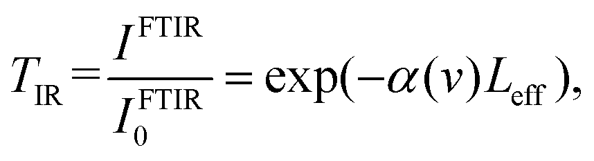
The conventional FTIR method is based on the Michelson interferometry scheme. In these measurements, the interferogram detected using a point detector is given by Fourier transform as a function of the difference in pathlength δ in the Michelson interferometer:16where ν = 1/λ is the wavenumber for the light source with wavelength λ (in centimetres) and S(ν) is the spectral intensity of light given by:


When an absorbing medium with thickness Leff is introduced into the system, the interferogram undergoes changes as per the Beer–Lambert law. Then, the ratio of two interferograms determines the transmittance of a sample:
The Q-IR imaging method is also based on the Michelson interferometry scheme (see the Materials and methods section). The wide-field interferogram, measured via this method using a visible range camera, is as follows:17–19
I(φ)QIR ∼ (1 + μ|τ|IR![[thin space (1/6-em)]](https://www.rsc.org/images/entities/char_2009.gif) cos(φ)), cos(φ)), |
| |τ(v)|IR = exp(−α(v)Leff/2). |
where I(φ)QIR is the interference pattern detected in the visible range,  is the amplitude transmission of the correlated probe IR light through a specimen, μ is the normalized first-order correlation function of the light source, and φ is the relative phase difference between interferometer arms.
In Q-IR imaging, the captured interference patterns depend on the amplitude transmission of the probe IR photons through sample τ, which contrasts with conventional methods, where absorption depends on the light intensity or T = τ2. As a result, the Q-IR method can potentially allow imaging through twice ticker specimens compared to using conventional techniques. Furthermore, in Q-IR imaging, the intensity level of the signal remains the same, only the visibility of the interferogram changes.
Substrate preparation
For the preparation of microfluidic devices, a four-inch silicon wafer was coated with a chromium/gold double layer using an e-beam evaporator (10/50 nm thickness). The coating was used to increase the IR reflectivity of the surface of the wafer.Subsequently, the Cr/Au coating was patterned with the layout of the microfluidic device by removing the excess metal layer via wet etching. The removal of the excess metal was performed to facilitate bonding of the exposed silicon with the microfluidic layer containing a CaF2 window, which was fabricated later. Briefly, an AZ5214E photoresist (Merck Performance Materials GmbH, Germany) was coated at 3000 rpm for 40 s and baked on a hot plate for 1.5 min at 100 °C. The photoresist was developed after exposure to 365 nm UV light through an optical mask on a mask aligner (MJB4, SÜSS MicroTec SE, Germany) to a total of 140 mJ cm−2. The wafer was then immersed in a gold etchant (Sigma Aldrich) for 40 s, washed with DI water, immersed in a chromium etchant (Sigma Aldrich) for 20 s, washed a second time with DI water, and finally dried in an N2 flow. Later, the photoresist was removed by immersing the wafer in an acetone bath, washed with isopropanol, and dried in an N2 flow. More detailed description of the fabrication procedure is available in the ESI, see section 1 and Fig. S1.†
SU-8 pattern preparation
We designed a simple pattern comprising arrays of squares with different sizes and gaps for identifying both the detection limit of our technique and the spatial resolution performances, see Fig. 1(c). A fully detailed fabrication protocol is given in the ESI.† Briefly, the gold-patterned substrate prepared in the previous section was spin-coated with a 14.5 μm thick layer of SU-8 3010 (Kayaku Advanced Materials, MA, USA). The resist was pre-baked for 10 min at 95 °C and then exposed for a total dose of 150 mJ cm−2 with UV light (365 nm) through a soda lime optical mask. The pattern was then post-baked for 3 min at 95 °C and developed. The final thickness of the SU-8 micropattern was confirmed by measuring the step height using a Bruker stylus profiler. Finally, the completed wafer was diced to the final size for a single device. A four-inch silicon wafer can produce three patterned substrates. | ||
| Fig. 1 The design layout of three photomasks for the fabrication of the microfluidic devices. (a) Layout of the first photomask to fabricate the SU-8 master mold. The SU-8 mold is used to fabricate the first half of the microfluidic device, which will eventually define the microfluidic chamber thickness. Shaded area: chrome in the photomask. (b and c) Layouts of the second and third photomasks to fabricate the second half of the microfluidic device. (b) Layout of the second photomask to pattern the gold layer on the silicon substrate. Shaded area: clear in the photomask. (c) Layout and dimensions of the third photomask to pattern the SU-8 square array after patterning the gold layer. Shaded area: clear in the photomask. The layout of (b) is based on (a), with features smaller on all sides for easier alignment with the first half of the device. | ||
Microfluidic chamber fabrication
The fabrication of the microfluidic chambers is based on the method disclosed previously in ref. 30 and 31 with some modifications. A detailed description of the modified method is available in the ESI.†Fig. 2 shows a schematic of this procedure and a picture of a resulting device. In this work, we fabricated three SU-8 molds with three different thicknesses. The resulting microfluidic chambers have 15 ± 1 μm, 26 ± 2 μm, and 44 ± 2 μm thicknesses. For the versions with chambers’ thicknesses of 26 and 44 μm, we used PDMS (Dow Corning Sylgard 184) mixed at the standard 10:1 ratio to fill by capillarity the cavity created between the device mold, the CaF2 window (Crystran Ltd, Dorset, UK), and the flat PDMS cut, which was used to make sure that the top surface of the resulting device is flat. The 15 μm thick device was fabricated using a low-viscosity UV-curable resin (NOA73, Norland Products, Jamesburg, NJ, USA) instead of PDMS, since PDMS is unable to efficiently flow within such a thin cavity. Once produced, the CaF2-containing microfluidic layer and the SU-8/Au-patterned substrate (prepared in the previous section) were treated with O2 plasma to activate the surfaces. They were then brought into contact immediately after plasma activation and kept pressed together to ensure permanent bonding.
 | ||
| Fig. 2 (a) 3D view schematic of the first half of the device, showing the microfluidic chamber structure on top of a CaF2 window. (b) 3D view schematic of the second half of the device, showing the SU-8 square array on top of a Cr/Au layer patterned on a silicon substrate. (c) 3D view schematic of the completed microfluidic device formed by bonding the first and second halves. (d) Side view schematics of the completed device. (e) Representative picture of the actual microfluidic device (the inset shows an optical image of the SU-8 pattern). | ||
Step height measurements
For the measurement of the step heights of the NOA73 or PDMS microfluidic layers, we used a Bruker stylus profiler, setting for a scan length of 10 mm and with an applied load of 1 mg from the spring activating the stylus (which has a tip radius of 12.5 μm, according to the vendor). The results of the scan are presented in Fig. S2 of the ESI.†The heights of the microfluidic chambers after assembly were determined using an optical reflectometer (Fr-pRo Vis/NIR, ThetaMetrisis, Athens, Greece) equipped with a 20× objective, which we used to focus on the SU-8 structures. The results and details of the procedure are presented in section 3 of the ESI.†
FTIR imaging
FTIR imaging measurements were carried out at the infrared beamline SISSI-Bio32 at the Elettra synchrotron light source. Hyperspectral images in the mid-IR were recorded using a Hyperion 3000 IR/VIS microscope (Bruker Optics, Billerica, MA, US) coupled with a vacuum interferometer (VERTEX 70 V, Bruker Optics, Billerica, MA, US) in reflection mode using a 15× objective and a 64 × 64 pixel focal plane array (FPA) detector as internal sources. The selected optical setup allows a pixel size of 2.67 micron. Data were collected by averaging 128 scans at 8 cm−1, setting the interferometer scanner speed at 5 kHz. Next, the data were pre-processed using OPUS 8.7, and then analysed using QUASAR (https:\\quasar.codes).33,34 Images were obtained using QUASAR and graphs were plotted with Origin PRO 2023 (OriginLab Corporation, MA, USA).Q-IR imaging
Fig. 3 shows a schematic of the design of the Q-IR microscopy system. In this method, a 532 nm continuous-wave pump laser was used to generate type-0 frequency non-degenerate spontaneous parametric down conversion (SPDC) photon pairs in a periodically poled lithium niobate (PPLN) crystal. The crystal has several poling periods, and it was placed on top to the heating stage. By temperature tuning, one photon from the pair (idler) can be set from 2.8 to 3.6 μm, while the conjugate photon (signal) has 657–624 nm wavelength accordingly. After the PPLN crystal, the visible photons (signal and pump) and IR photons were split by a shortpass dichroic beam splitter DM2 into two arms of the Michelson interferometer. Next, visible photons were focused onto the reference mirror M by lens F1 (f1 = 100 mm), while IR photons were focused into the sample by the IR objective lens. To capture and retrieve the absorption image of the sample, one needs to scan the phase images.35–38 Thus, the sample was placed on an XYZ positioner and a piezo stage to perform imaging and phase scanning, respectively.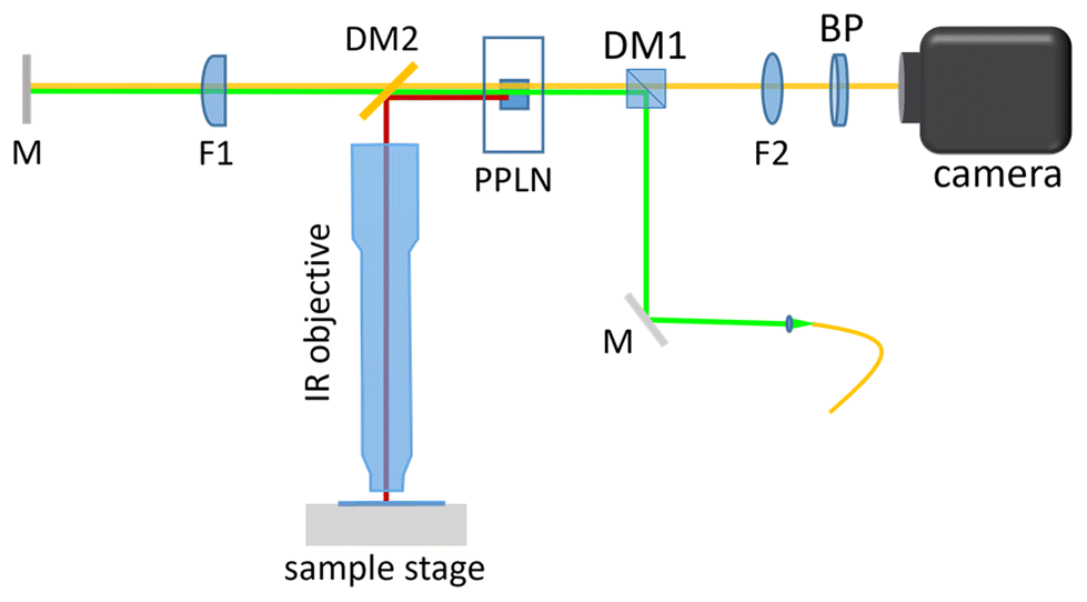 | ||
| Fig. 3 Scheme of the Q-IR imaging set-up (Michelson interferometer): M is a mirror, DM1 and 2 are dichroic mirrors, F1 and 2 are lenses, and BP is a bandpass filter. | ||
After reflecting from the reference mirror and the sample, the photons were recombined back to the nonlinear crystal, where the reflected pump beam generates another SPDC photon pair. Then, a standard silicon CMOS camera for the visible range and an achromatic lens F2 (f2 = 75 mm) were used for capturing the interference pattern for the signal photons.
Results
Results of Q-IR and FTIR imaging
We used our Q-IR system to acquire wide field IR images of the SU-8 pattern in the microfluidic chambers, both without and with filled with water. We collected our data for the range of IR wavelengths between 2.8 μm and 3.6 μm. The current configuration of the Q-IR system uses the reflection mode of imaging, where the probing light passes twice inside the medium of interest. This means that the effective path length Leff of the photons inside the device is 30 μm (C1), 52 μm (C2), and 88 μm (C3), respectively. Given that the thickness of the SU-8 layer is 14.5 μm, the water layer thickness in each of device over the SU-8 features is 1 μm (C1), 23 μm (C2) and 59 μm (C3), respectively, for a double pass of the probe photons. In C3, the water layer thickness above the SU-8 patterns is over double that of C2.First, we imaged microfluidic devices without water. Images at 2846 nm, 3220 nm, 3429 nm and 3505 nm wavelengths are presented in Fig. 4(a)–(d), respectively. The dark regions in the images correspond to higher absorption of IR light by the SU-8 photoresist, while the clear regions correspond to lower absorption. The smallest features of the SU-8 pattern, 5 μm side length squares, were still resolved by the Q-IR system, which agrees with our resolution measurements, see section 8 of the ESI.† We also note that the absorption of the SU-8 photoresist is higher at 2846 nm and 3429 nm wavelengths. Then, we plotted the respective IR absorption spectra for the five square regions of interest highlighted by different colours in Fig. 4(a)–(d), corresponding to the SU-8 pattern, see Fig. 4(e). The results are in a good agreement with the FTIR measurements shown by the solid blue curve, indicating the –OH and –C–H– stretching absorption bands. Details of how the images and the spectra are generated are given in the ESI, section 4.†
 | ||
| Fig. 4 (a–d) IR images of the microfluidic chip without being filled with water, taken using a Q-IR microscopy system. The images in (a–d) show the visibility map of the interference pattern at probe (idler) wavelengths of 2846 nm, 3220 nm, 3429 nm, and 3505 nm, respectively. (e) IR absorption spectra of the SU-8 photoresist calculated for five square regions of interest highlighted by different colours in (a)–(d): black, green, red, pink, and blue. | ||
Next, we filled the microfluidic chips with water and performed IR imaging using Q-IR and FTIR methods in the wavelength range of 3.3 μm–3.6 μm, some of which are presented in Fig. 5. Images shown in the first, second and third panels correspond to the results taken with chips C1, C2 and C3 filled with water, respectively. The top images in each panel correspond to Q-IR imaging, while the images below them show the results obtained via FTIR measurements. The columns from left to right correspond to 3314 nm, 3352 nm, 3390 nm, and 3429 nm of probing wavelengths, respectively.
 | ||
| Fig. 5 Q-IR and FTIR absorption images of the three devices obtained after being filled with water. The chamber heights are 15 μm (C1), 26 μm (C2), and 44 μm (C3). The square features are the SU-8 pattern with a width of 50 μm. Device C2 was filled with water only partially; the red-dotted lines show the boundary between water and air. The intensity scale bar next to the Q-IR images shows the absorption intensity in percentage; the one next to the FTIR images represent the absorption intensity in A.U. The black scale bars in the FTIR images are 50 μm long. | ||
In the Q-IR images captured at the 3314 nm wavelength, the areas surrounding the SU-8 resist pattern appear darker compared to other wavelengths due their proximity to the strongest absorption line of water at 2898 nm. Water absorption decreases at longer wavelengths, enabling imaging of the SU-8 pattern within microfluidic chips C1 and C2, and partially in C3.
In chips C1 and C2, the IR absorption of water allows for imaging of the SU-8 pattern at all wavelengths. There is a clear contrast in the absorption map for the SU-8 pattern and the surrounding area. Note that the edges of the SU-8 pattern appear darker due to scattering losses. On the other hand, inside chamber C3, water absorption is too strong at 3314 nm and 3352 nm wavelengths. However, the SU-8 pattern is still observed starting from the 3390 nm wavelength, see also Fig. S4.† As a result, Q-IR imaging adequately displays the IR absorption maps both for the SU-8 resist and an about 30 μm water layer on top of the test patterns. The results clearly demonstrate the decrease of water absorption at longer wavelengths, and absorption contrast of the SU-8 pattern, which agrees with the FTIR results.
The corresponding FTIR images follow the same trend, where the chemical contrast is clear in devices C1 and C2, and it is possible to observe the change in contrast to water to resist with wavelength changes. In C2, the contrast is reduced due to the thicker water layer. Upon filling the C2 device with water, the presence of trapped air bubbles is observed, see also Fig. S5.† The variation in absorption of the SU-8 layer is less evident with the water layer on top, while the contrast is more distinct in the air-filled region. In the images for device C3, the contrast is reduced even more, and the SU-8 structures are detectible due to scattering occurring at the edges of the pattern. However, from these images and the relative spectra (shown in Fig. S6 of the ESI†), it is noticeable that the chemical contrast in the FTIR images is nearly lost. This observation is also supported by the cross sections of IR images over a line crossing the SU-8 features, see Fig. S7 and S8 of the ESI.†
Discussion and conclusions
In this work, we discussed the capability of the Q-IR imaging system to deal with the strong absorption band of water in the mid-IR range. We fabricated a set of microfluidic devices with three controlled channel heights and comprising a test pattern made of a well-known material. This was done to experimentally determine the maximum thickness of the water layer through which we could still detect a reliable absorption image of the SU-8 pattern. As a benchmark, we compared our results with the imaging capabilities of a standard FTIR microscope. The FTIR microscope was equipped with an FPA, collecting hyperspectral datasets in the whole mid-IR region. Images were produced by integrating the absorption spectra in a narrow band centred around the frequency points that we investigated with our Q-IR imaging system. Even though it would be fairer to compare our system with other similar approaches using discrete or monochromatic light sources (such as quantum cascade lasers), FTIR is still the state-of-the-art in terms of standard IR microscopy.The presented results show that it is possible to image through an about 12 μm thick water layer in the entire range from 2.8 to 3.6 μm wavelengths. The image quality and resolution of Q-IR are comparable to those acquired on the same samples with the FTIR set-up. From the results, the water –OH stretching band starts to appear as we move towards shorter wavelengths with increasing water absorption. We can also recognize the change from lower to higher absorption of the test SU-8 pattern as we scan from 3.3 μm to 3.4 μm, which corresponds to the range usually attributed to aromatic –CH absorption bands.39 This peak is reported in the re-constructed spectrum shown in Fig. 4. The abovementioned spectral region is of interest in view of the presence of lipid-associated absorption peaks, which can be used for studies of biological tissues and cells.
In device C3, with a water column of about 30 μm above the SU-8 structures, we can observe Q-IR images of the SU-8 pattern appearing in the higher wavelength range, i.e. around and above 3.4 μm. Here the –OH stretching band in water appears to be fading out and the absorption of the sample, if any, becomes predominant (see also Fig. S4 in the ESI† where we plot the visibility through 44 μm height of water, which proves that the measurable signal starts from the 3.39 μm wavelength). We note that even though structures are visible in the images produced by the FTIR set-up, they are strongly affected by noise. Moreover, the contrast in the series of images at increasing wavelength does not show any significant dynamic changes, making it impossible to deduce the features of the absorption peaks (see also Fig. S7 and S8 in the ESI†).
Based on these results, we conclude that our Q-IR microscope allows for measuring the absorption spectrum in the mid-IR region where the biological components of interest can be found, such as lipids, even in the presence of an up to 30 μm thick water layer (in reflection mode). A transmission configuration, for instance, a Mach–Zehnder interferometer, can be used for Q-IR imaging as well. In this case, the constraints for the thickness of the microfluidics can be relaxed further due to a single pass through the sample. This would further make the design and fabrication of microfluidic devices for IR microscopy of biological tissues and live cells much easier, while allowing the experimental conditions to be less stressful for the sample. This is particularly important because compression and constriction are known to affect the behaviour of live cells,40–42 since cells adhering to a substrate can be thicker than 10 μm, especially in the region of the nucleus.
We expect that the relaxed conditions allowed by Q-IR microscopy would enable more reliable studies of live cells. Moreover, in the future, these devices could be extended from the study of single cells in monolayers to multilayers or small organoids. It is worth stressing that although Q-IR does not perform as well as state-of-the-art FTIR in terms of spatial resolution and speed of acquisition, it outperforms in terms of signal-to-noise ratio. This improvement can be attributed to the detection sensor in our system, which is a standard CMOS camera for the visible wavelength range, operating at room temperature. This contrasts with IR detectors, such as bolometers and MCT photodetectors, suffering from their own components emitting room temperature black-body radiation, which requires them to operate at cryogenic temperatures.
As a result, we demonstrate that Q-IR provides image quality at least comparable to that of FTIR imaging. However, the Q-IR method achieves better identification of chemical composition (see Fig. S9 and S10†), whereas FITR imaging may display artifacts due to analytical calculations. As such, we believe that Q-IR microscopy provides a viable alternative to FTIR, especially for biological analysis without the need for more expensive set-ups.
Author contributions
GG and AP conceptualized and led the experiments. MS, TP, JVS, HY, LK and GB provided the samples and performed the measurements and data analysis. All co-authors contributed to the discussion and interpretation of the data and the writing of the manuscript.Data availability
The data supporting this article have been included as part of the ESI.†Conflicts of interest
The authors have no conflicts of interest to declare.Acknowledgements
G. G. acknowledges support to this research by MBI and NUS through an internal seed grant. A. P. and T. P. acknowledge the support by A*STAR with grant no. C230917004 and Q.InC Strategic Research and Translational Thrust. G. G. and A. P. acknowledge support to this research by the NRF (Singapore) through the grant NRF2021-QEP2-03-P08. A. P. and T. P. acknowledge the valuable suggestions from Zi S. D. Toa regarding the data analysis procedures. We acknowledge the help of A. W. Min-Shang for editing the manuscript.References
- W. Yang, L. Hou and C. Luo, When Super-Resolution Microscopy Meets Microfluidics: Enhanced Biological Imaging and Analysis with Unprecedented Resolution, Small, 2023, 19(23), 2207341 CrossRef CAS PubMed.
- C. Simonnet and A. Groisman, High-Throughput and High-Resolution Flow Cytometry in Molded Microfluidic Devices, Anal. Chem., 2006, 78(16), 5653–5663 CrossRef CAS PubMed.
- W. Busch, et al., A microfluidic device and computational platform for high-throughput live imaging of gene expression, Nat. Methods, 2012, 9(11), 1101–1106 CrossRef CAS PubMed.
- L. Bell, et al., A microfluidic device for the hydrodynamic immobilisation of living fission yeast cells for super-resolution imaging, Sens. Actuators, B, 2014, 192, 36–41 CrossRef CAS PubMed.
- M. Nourmohammadzadeh, et al., A microfluidic array for real-time live-cell imaging of human and rodent pancreatic islets, Lab Chip, 2016, 16(8), 1466–1472 RSC.
- J. Doherty, G. Cinque and P. Gardner, Single-cell analysis using Fourier transform infrared microspectroscopy, Appl. Spectrosc. Rev., 2017, 52(6), 560–587 CrossRef CAS.
- M. Fuest, et al., In situ Microfluidic Cryofixation for Cryo Focused Ion Beam Milling and Cryo Electron Tomography, Sci. Rep., 2019, 9(1), 19133 CrossRef CAS PubMed.
- J. Ahn, et al., Modeling of three-dimensional innervated epidermal like-layer in a microfluidic chip-based coculture system, Nat. Commun., 2023, 14(1), 1488 CrossRef CAS PubMed.
- L. Amirifar, et al., Brain-on-a-chip: Recent advances in design and techniques for microfluidic models of the brain in health and disease, Biomaterials, 2022, 285, 121531 CrossRef CAS PubMed.
- F. Duzagac, et al. Microfluidic Organoids-on-a-Chip: Quantum Leap in Cancer Research, Cancers, 2021, 13(4), 737 CrossRef PubMed.
- A. Shimizu, et al., ECM-based microchannel for culturingin vitrovascular tissues with simultaneous perfusion and stretch, Lab Chip, 2020, 20(11), 1917–1927 RSC.
- Y. Jun, et al., In vivo–mimicking microfluidic perfusion culture of pancreatic islet spheroids, Sci. Adv., 2019, 5(11), eaax4520 CrossRef CAS PubMed.
- J. Ko, et al., Tumor spheroid-on-a-chip: A standardized microfluidic culture platform for investigating tumor angiogenesis, Lab Chip, 2019, 19(17), 2822–2833 RSC.
- T. P. Wrobel and R. Bhargava, Infrared Spectroscopic Imaging Advances as an Analytical Technology for Biomedical Sciences, Anal. Chem., 2018, 90(3), 1444–1463 CrossRef CAS PubMed.
- H. A. Bechtel, et al., Ultrabroadband infrared nanospectroscopic imaging, Proc. Natl. Acad. Sci. U. S. A., 2014, 111(20), 7191–7196 CrossRef CAS PubMed.
- P. R. Griffiths and J. A. d. Haseth, Fourier Transform Infrared Spectrometry, John Wiley & Sons, Inc., New York, 2007, pp. i–xvii Search PubMed.
- G. B. Lemos, et al., Quantum imaging with undetected photons, Nature, 2014, 512(7515), 409–412 CrossRef CAS PubMed.
- A. V. Paterova, et al., Hyperspectral infrared microscopy with visible light, Sci. Adv., 2020, 6(44), eabd0460 CrossRef CAS PubMed.
- I. Kviatkovsky, et al., Microscopy with undetected photons in the mid-infrared, Sci. Adv., 2020, 6(42), eabd0264 CrossRef CAS PubMed.
- P. I. Haris and D. Chapman, Does Fourier-transform infrared spectroscopy provide useful information on protein structures?, Trends Biochem. Sci., 1992, 17(9), 328–333 CrossRef CAS PubMed.
- K. Rahmelow and W. Hubner, Infrared Spectroscopy in Aqueous Solution: Difficulties and Accuracy of Water Subtraction, Appl. Spectrosc., 1997, 51(2), 160–170 CrossRef CAS.
- S. Venyaminov and F. G. Prendergast, Water (H2O and D2O) molar absorptivity in the 1000–4000 cm-1 range and quantitative infrared spectroscopy of aqueous solutions, Anal. Biochem., 1997, 248(2), 234–245 CrossRef CAS PubMed.
- V. Zohdi, et al., Importance of Tissue Preparation Methods in FTIR Micro-Spectroscopical Analysis of Biological Tissues: ‘Traps for New Users’, PLoS One, 2015, 10(2), e0116491 CrossRef PubMed.
- D. Hartnell, et al., Mapping sub-cellular protein aggregates and lipid inclusions using synchrotron ATR-FTIR microspectroscopy, Analyst, 2021, 146(11), 3516–3525 RSC.
- M. R. Alcaráz, et al., External-Cavity Quantum Cascade Laser Spectroscopy for Mid-IR Transmission Measurements of Proteins in Aqueous Solution, Anal. Chem., 2015, 87(13), 6980–6987 CrossRef PubMed.
- Z. Movasaghi, et al., Fourier Transform Infrared (FTIR) Spectroscopy of Biological Tissues, Appl. Spectrosc. Rev., 2008, 43(2), 134–179 CrossRef CAS.
- E. Harasim, et al., Myocardial Lipid Profiling During Time Course of High Fat Diet and its Relationship to the Expression of Fatty Acid Transporters, Cell. Physiol. Biochem., 2015, 37(3), 1147–1158 CrossRef CAS PubMed.
- U. L. Kelly, et al., High-density lipoproteins are a potential therapeutic target for age-related macular degeneration, J. Biol. Chem., 2020, 295(39), 13601–13616 CrossRef CAS PubMed.
- G. C. Sparagna, et al., Loss of cardiac tetralinoleoyl cardiolipin in human and experimental heart failure, J. Lipid Res., 2007, 48(7), 1559–1570 CrossRef CAS PubMed.
- G. Birarda, et al., IR-Live: Fabrication of a low-cost plastic microfluidic device for infrared spectromicroscopy of living cells, Lab Chip, 2016, 16(9), 1644–1651 RSC.
- M. Suryana, et al., Soft Lithographic Procedure for Producing Plastic Microfluidic Devices with View-ports Transparent to Visible and Infrared Light, J. Visualized Exp., 2017,(126), e55884 Search PubMed.
- G. Birarda , et al., Chemical analyses at micro and nano scale at SISSI-Bio beamline at Elettra-Sincrotrone Trieste, in Progress in Biomedical Optics and Imaging – Proceedings of SPIE, 2022.
- M. Toplak, et al., Infrared Orange: Connecting Hyperspectral Data with Machine Learning, Synchrotron Radiat. News, 2017, 30(4), 40–45 CrossRef.
- M. Toplak, et al., Quasar: Easy Machine Learning for Biospectroscopy, Cells, 2021, 10(9), 2300 CrossRef PubMed.
- A. V. Paterova, et al., Quantum imaging for the semiconductor industry, Appl. Phys. Lett., 2020, 117(5), 054004 CrossRef CAS.
- M. Gilaberte Basset, et al., Video–Rate Imaging with Undetected Photons, Laser Photonics Rev., 2021, 15, 2000327 CrossRef.
- B. E. Haase, et al., Phase-quadrature quantum imaging with undetected photons, Opt. Express, 2023, 31(1), 143–152 CrossRef PubMed.
- E. Pearce, et al., Practical quantum imaging with undetected photons, Opt. Continuum, 2023, 2(11), 2386–2397 CrossRef CAS.
- E. Mitri, et al., SU-8 bonding protocol for the fabrication of microfluidic devices dedicated to FTIR microspectroscopy of live cells, Lab Chip, 2014, 14(1), 210–218 RSC.
- R. K. Jain, J. D. Martin and T. Stylianopoulos, The Role of Mechanical Forces in Tumor Growth and Therapy, Annu. Rev. Biomed. Eng., 2014, 16(1), 321–346 CrossRef CAS PubMed.
- D. Song, et al., Cell-induced confinement effects in soft tissue mechanics, J. Appl. Phys., 2021, 129(14), 140901 CrossRef CAS.
- C. P. Brangwynne, et al., Microtubules can bear enhanced compressive loads in living cells because of lateral reinforcement, J. Cell Biol., 2006, 173(5), 733–741 CrossRef CAS PubMed.
Footnotes |
| † Electronic supplementary information (ESI) available. See DOI: https://doi.org/10.1039/d4an01201a |
| ‡ Current address: Laboratory of Quantum Engineering of Light, South Ural State University, Chelyabinsk 454080, Russia. |
| This journal is © The Royal Society of Chemistry 2025 |